ICST AV94206F-T, ICS94206F-T Datasheet
Integrated
Circuit
Systems, Inc.
ICS94206
94206 Rev B 04/26/01
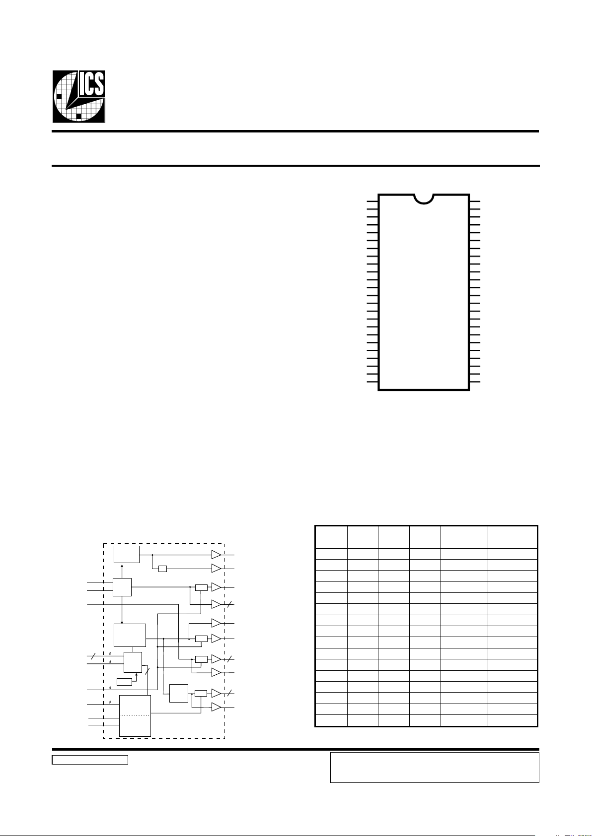
Pin Configuration
Recommended Application:
440BX - VIA Apollo Pro133 - ALI 1631 style chipset.
Output Features:
• 2 - CPUs @2.5V
• 1 - IOAPIC @ 2.5V
• 13 - SDRAM @ 3.3V
• 6 - PCI @3.3V,
• 1 - 48MHz, @3.3V
• 1 - 24MHz @ 3.3V
• 2 - REF @3.3V, 14.318MHz.
Features:
• Programmable ouput frequency.
• Programmable ouput rise/fall time.
• Programmable PCI_F and PCICLK skew.
• Spread spectrum for EMI control typically by 7dB to
8dB,
with programmable spread percentage.
• Watchdog timer technology to reset system
if over-clocking causes malfunction.
• Uses external 14.318MHz crystal.
• FS pins for frequency select
Key Specifications:
• CPU – CPU: <175ps
• SDRAM - SDRAM: <500ps
• PCI – PCI: <500ps
• CPU(early)-PCI: Min=1.0ns, Typ=2.0ns, Max=4.0ns
Programmable System Frequency Generator for PII/III™
Block Diagram
48-Pin 300mil SSOP
CLK_STOP#
PCI_STOP#
PLL2
PLL1
Spread
Spectrum
48MHz
24MHz
IOAPIC
CPUCLK_F
CPUCLK 1
SDRAM (11:0)
PCICLK (4:0)
PCICLKF
SDRAM_F
X1
X2
BUFFER IN
XTAL
OSC
PCI
CLOCK
DIVDER
STOP
STOP
STOP
STOP
S DATA
SCLK
FS(3:0)
MODE
Control
Logic
Config.
Reg.
/2
REF(1:0)
LATCH
POR
2
12
5
4
4
VDD1
*PCI_STOP/REF0
GND
X1
X2
VDD2
*MODE/PCICLK_F
**FS3/PCICLK0
GND
PCICLK1
PCICLK2
PCICLK3
PCICLK4
VDD2
BUFFER IN
GND
SDRAM11
SDRAM10
VDD3
SDRAM9
SDRAM8
GND
S DATA
SCLK
VDDL1
IOAPIC
REF1/FS2*
GND
CPUCLK_F
CPUCLK1
VDDL2
CLK_STOP#*
SDRAM_F
GND
SDRAM0
SDRAM1
VDD3
SDRAM2
SDRAM3
GND
SDRAM4
SDRAM5
VDD3
SDRAM6
SDRAM7
VDD4
48MHz/FS0*
24MHz/FS1*
ICS94206
1
2
3
4
5
6
7
8
9
10
11
12
13
14
15
16
17
18
19
20
21
22
23
24
48
47
46
45
44
43
42
41
40
39
38
37
36
35
34
33
32
31
30
29
28
27
26
25
* Internal Pull-up Resistor of 120K to VDD
** Internal Pull-down resistor of 120K to GND
Functionality
3SF2SF1SF0SF
UPC
)zHM(
KLCICP
)zHM(
0000 00.0800.04
0001 00.5705.73
0010 13.3856.14
0011 28.6614.33
0100 00.30133.43
0101 10.21143.73
0110 10.8610.43
0111 32.00114.33
1000 00.02100.04
1001 99.41133.83
1010 99.90166.63
1011 00.50100.53
1100 00.04100.53
1101 00.05105.73
1110 00.42100.13
1111 99.23152.33
ICS reserves the right to make changes in the device data identified in
this publication without further notice. ICS advises its customers to
obtain the latest version of all device data to verify that any
information being relied upon by the customer is current and accurate.
2
ICS94206
General Description
Pin Configuration
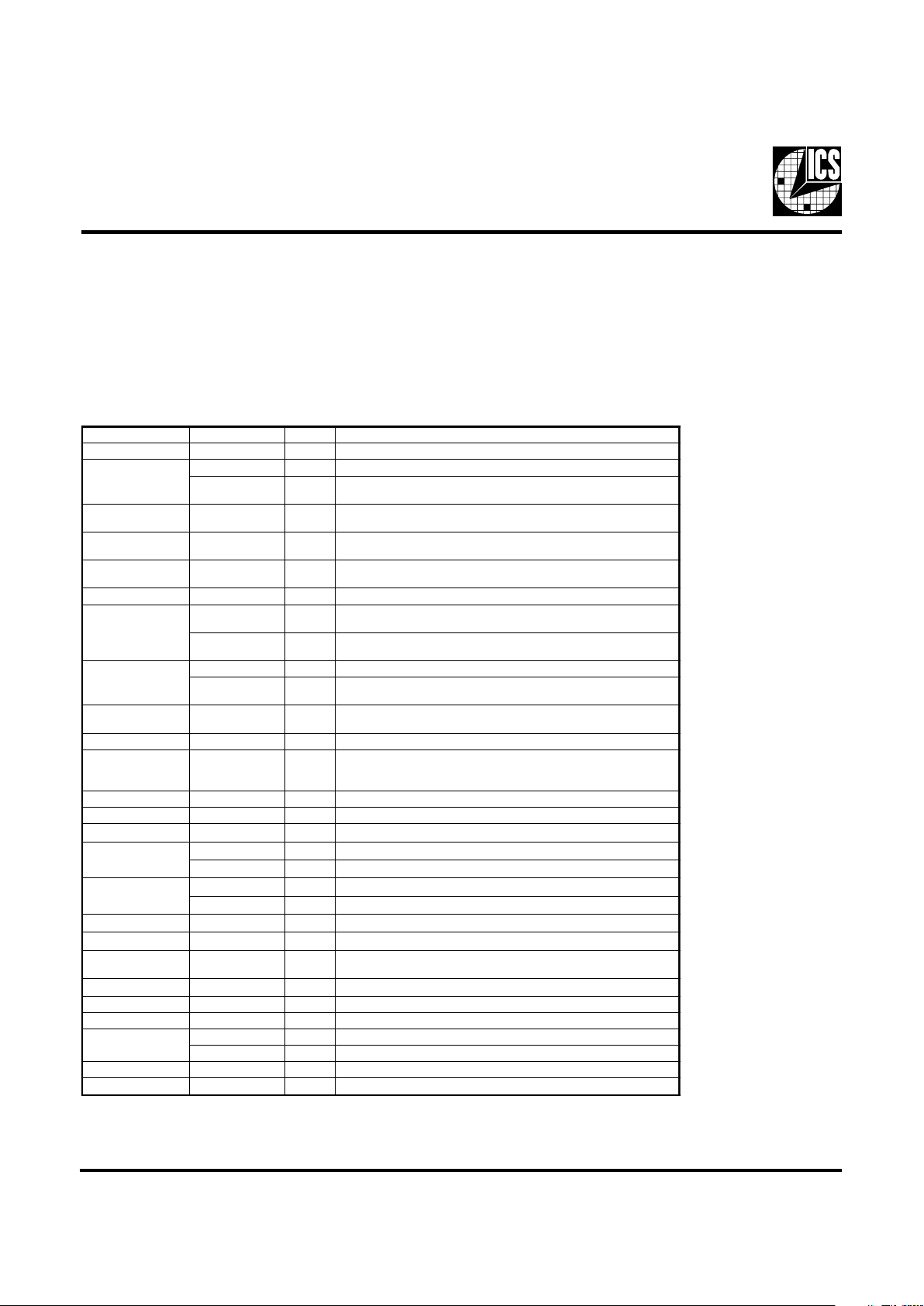
The ICS94206 is a single chip clock solution for desktop designs using the BX/Apollo Pro133/ALI 1631 style chipset. It provides all
necessary clock signals for such a system.
The ICS94206 belongs to ICS new generation of programmable system clock generators. It employs serial programming I
2
C
interface as a vehicle for changing output functions, changing output frequency, configuring output strength, configuring output to
output skew, changing spread spectrum amount, changing group divider ratio and dis/enabling individual clocks. This device also
has ICS propriety 'Watchdog Timer' technology which will reset the frequency to a safe setting if the system become unstable from
over clocking.
Notes:
1: Internal Pull-up Resistor of 120K to 3.3V on indicated inputs
2: Bidirectional input/output pins, input logic levels are latched at internal power-on-reset. Use 10Kohm resistor
to program logic Hi to VDD or GND for logic low.
REBMUNNIPEMANNIPEPYTNOITPIRCSED
11DDVRWPV3.3lanimon,ylppusrewopLATX,feR
2
0FERTUO.kcolcecnereferzhM813.41
#POTS_ICP
1
NI
elibomnI(woltupninehw,level0cigoltaskcolcKLCICPstlaH
)0=EDOM,edom
,22,61,9,3
54,93,33
DNGRWPdnuorG
41XNI
kcabdeefdna)Fp63(pacdaollanretnisah,tupnilatsyrC
2Xmorfrotsiser
52XTUO
daollanretnisaH.zHM813.41yllanimon,tuptuolatsyrC
)Fp63(pac
41,62DDVRWPV3.3lanimon,)4:0(KLCICPdnaF_KLCICProfylppuS
7
F_KLCICPTUO
rewoprof#POTS_ICPybdetceffatonkcolcICPgninnureerF
.tnemeganam
EDOM
2,1
NI
.edoMeliboM=0,edoMpotkseD=1,niptcelesnoitcnuf7niP
.tupnIdehctaL
8
3SFNIDNGotnwod-lluPlanretnI.tupnIdehctaL.niptcelesycneuqerF
0KLCICPTUO
wekssn84-1htiwskcolcUPCotsuonorehcnyS.stuptuokcolcICP
)ylraeUPC(
01,11,21,31)1:4(KLCICPTUO
wekssn84-1htiwskcolcUPCotsuonorehcnyS.stuptuokcolcICP
)ylraeUPC(
51NIREFFUBNI.stuptuoMARDSrofsreffuBtuonaFottupnI
,12,02,81,71
,23,13,92,82
83,73,53,43
)0:11(MARDSTUO
nipNIREFFUBmorfstuptuoreffuBtuonaF,stuptuokcolcMARDS
.)tespihcybdellortnoc(
63,03,913DDVRWP.V3.3lanimon,eroCLLPUPCdna)21:0(MARDSrofylppuS
32ATADSO/IIrofnipataD
2
tnarelotV5yrtiucricC
42KLCSNIIfotupnikcolC
2
tupnitnarelotV5,tupniC
52
zHM42TUOkcolctuptuozHM42
1SF
2,1
NI.tupnIdehctaL.niptcelesycneuqerF
62
zHM84TUOkcolctuptuozHM84
0SF
2,1
NItupnIdehctaL.niptcelesycneuqerF
724DDVRWP.erocLLPdexifdnasreffubtuptuozHM84&42rofrewoP
04F_MARDSTUO#POTS_UPCybdetceffatoN.tuptuokcolcMARDSgninnureerF
14#POTS_KLCNI
MARDS&CIPAOI,1KLCUPCstlahtupnisuonorhcnysasihT
.wolnevirdnehwlevel"0"cigolta)11:0(
242LDDVRWPlanimonV3.3roV5.2rehtie,skcolcUPCrofylppuS
341KLCUPCTUOwoL=#POTS_UPCfiwoL.2LDDVybderewop,stuptuokcolcUPC
44F_KLCUPCTUO#POTS_UPCehtybdetceffatoN.kcolcUPCgninnureerF
64
1FERTUO.kcolcecnereferzHM813.41
2SF
2,1
NItupnIdehctaL.niptcelesycneuqerF
74CIPAOITUOCIPAOI.1LDDVybderewoPzHM813.41.tuptuokcolc
841LDDVRWPlanimonV3.3ro5.2rehtie,CIPAOIrofylppuS
3
ICS94206
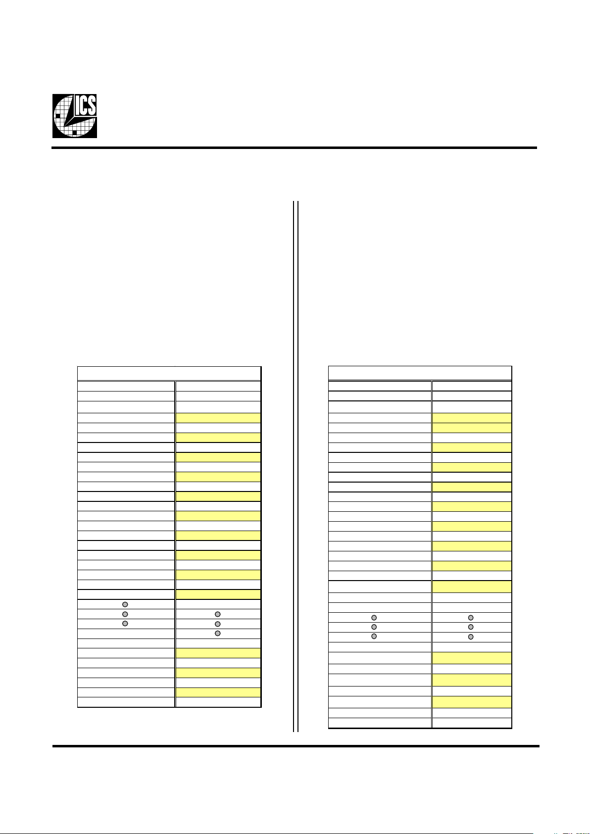
General I2C serial interface information for the ICS94206
How to Write:
• Controller (host) sends a start bit.
• Controller (host) sends the write address D2
(H)
• ICS clock will acknowledge
• Controller (host) sends a dummy command code
• ICS clock will acknowledge
• Controller (host) sends a dummy byte count
• ICS clock will acknowledge
• Controller (host) starts sending Byte 0 through Byte 20
(see Note)
• ICS clock will acknowledge each byte one at a time
• Controller (host) sends a Stop bit
How to Read:
• Controller (host) will send start bit.
• Controller (host) sends the read address D3
(H)
• ICS clock will acknowledge
• ICS clock will send the byte count
• Controller (host) acknowledges
• ICS clock sends Byte 0 through byte 8 (default)
• ICS clock sends Byte 0 through byte X (if X
(H)
was
written to byte 8).
• Controller (host) will need to acknowledge each byte
• Controller (host) will send a stop bit
Controll e r (Host)
ICS (Slave/Receiver)
Start Bit
Address D2
(H)
ACK
Dumm y Comm an d Code
ACK
Dumm y B y te Count
ACK
Byte 0
ACK
Byte 1
ACK
Byte 2
ACK
Byte 3
ACK
Byte 4
ACK
Byte 5
ACK
Byte 6
ACK
Byte 18
ACK
Byte 19
ACK
Byte 20
ACK
Stop Bit
How to Write:
*See notes on the following page.
Controlle r (Host)
ICS (Slave/Receiver)
Start Bit
Address D3
(H)
ACK
Byte Count
ACK
Byte 0
ACK
Byte 1
ACK
Byte 2
ACK
Byte 3
ACK
Byte 4
ACK
Byte 5
ACK
Byte 6
ACK
If 7
H
has been written to B 6
Byte 7
ACK
If 12
H
has been written to B 6
Byte18
ACK
If 13
H
has been written to B 6
Byte 19
ACK
If 14
H
has been written to B 6
Byte 20
ACK
Stop Bit
How to Read:

4
ICS94206
1. The ICS clock generator is a slave/receiver, I2C component. It can read back the data stored in the latches for verification.
Readback will support standard SMBUS controller protocol. The number of bytes to readback is defined by writing to
byte 8.
2. When writing to byte 11 - 12, and byte 13 - 14, they must be written as a set. If for example, only byte 14 is written
but not 15, neither byte 14 or 15 will load into the receiver.
3. The data transfer rate supported by this clock generator is 100K bits/sec or less (standard mode)
4. The input is operating at 3.3V logic levels.
5. The data byte format is 8 bit bytes.
6. To simplify the clock generator I
2
C interface, the protocol is set to use only Block-Writes from the controller. The bytes
must be accessed in sequential order from lowest to highest byte with the ability to stop after any complete byte has been
transferred. The Command code and Byte count shown above must be sent, but the data is ignored for those two bytes.
The data is loaded until a Stop sequence is issued.
7. At power-on, all registers are set to a default condition, as shown.
Notes:
Brief I2C registers description for ICS94206
Programmable System Frequency Generator
Register N ame Byte Description PWD D efau lt
Functionality & Frequency
Select Register
0
Output frequency, hardware / I
2
C
frequ ency s elect, spread spectrum &
output enable control register.
See individual
byte description
Output Con trol R egis ters 1-6
Active / inactive outpu t control
registers/latch inputs read back.
See individual
byte description
Vendor ID & Revision ID
Registers
7
Byte 11 bit[7:4] is ICS vendor id - 1001.
Other bits in this register designate device
revision ID of this part.
See individual
byte description
Byte Cou nt
Read Back Register
8
Writing to this regis ter w ill con figure
byte count and how many byte will be
read back. Do not write 00
H
to this by te.
08
H
Watchdog Timer
Count Register
9
Writing to this regis ter w ill con figure the
number of seconds for the watchdog
timer to res et.
10
H
Watchdog Control Registers 10 Bit [6:0]
Watchdog enable, watchdog status and
programmable 'safe' frequency' can be
confi
g
ured in th is register .
000,0000
VCO Control Selectio n Bit 10 Bit [7]
This bit s elect w heth er the outp ut
frequency is control by hardware/byte 0
configurations or byte 11&12
programming.
0
VCO Frequency Control
Registers
11-12
These registers control the dividers ratio
into the phase detector and thus control
the V CO output frequency.
Depended on
hardware/byte 0
configuration
Spread Spectrum Control
Registers
13-14
Thes e registers control the spread
percentage amount.
Depended on
hardware/byte 0
configuration
Group Skews Control
Registers
15-16
Increment or decrement the group skew
amount as com pared to th e initial s kew .
See individual
byte description
Output Rise/Fall Time
Select Registers
17-20
Thes e registers w ill control the output
rise and fall time.
See individual
byte description
5
ICS94206
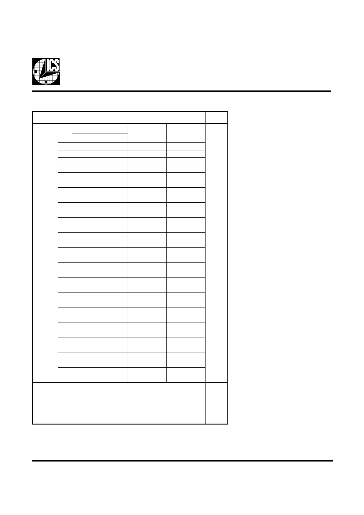
Byte 0: Functionality and frequency select register (Default=0)
Notes:
1.
Default at power-up will be for latched logic inputs to define frequency, as displayed by Bit 3.
tiB
noitpircseD
DWP
tiB
)4:7,2(
2tiB
7tiB6tiB5tiB4tiB
zHMKLCUPC
KLCICP
zHM
1etoN
3SF2SF1SF0SF
00000 00.0800.04
00001 00.5705.73
00010 13.3856.14
00011 28.6614.33
00100 00.30133.43
00101 10.21143.73
00110 10.8610.43
00111 32.00114.33
01000 00.02100.04
01001 99.41133.83
01010 99.90166.63
01011 00.50100.53
01100 00.04100.53
01101 00.05105.73
01110 00.42100.13
01111 99.23152.33
10000 00.53157.33
10001 99.92105.23
10010 00.62105.13
10011 00.81133.93
10100 89.51166.83
10101 00.5976.13
10110 00.0900.03
10111 10.5843.82
11000 00.66105.14
11001 10.06100.04
11010 99.45157.83
11011 59.74199.63
11100 89.54105.63
11101 89.34199.53
11110 99.14105.53
11111 10.83105.43
3tiB
stupnidehctal,tceleserawdrahybdetcelessiycneuqerF-0
4:7,2tiBybdetcelessiycneuqerF-1
0
1tiB
lamroN-0
daerpSretneC%53.0±elbanemurtcepsdaerpS-1
1
0tiB
gninnuR-0
stuptuollaetatsirT-1
0
6
ICS94206
Byte 1: CPU, Active/Inactive Register
(1= enable, 0 = disable)
Byte 2: PCI, Active/Inactive Register
(1= enable, 0 = disable)
TIB#NIPDWPNOITPIRCSED
7tiB-1 )devreseR(
6tiB71 F_KLCICP
5tiB-1 )devreseR(
4tiB311 4KLCICP
3tiB211 3KLCICP
2tiB111 2KLCICP
1tiB011 1KLCICP
0tiB81 0KLCICP
Notes:
1. Inactive means outputs are held LOW and are disabled
from switching.
2. Latched Frequency Selects (FS#) will be inverted logic
load of the input frequency select pin conditions.
TIB#NIPDWPNOITPIRCSED
7tiB-1 )devreseR(
6tiB-1 )devreseR(
5tiB-1 )devreseR(
4tiB-1 )devreseR(
3tiB-X #1SFdehctaL
2tiB-1 )devreseR(
1tiB-X #3SFdehctaL
0tiB-1 )devreseR(
Byte 4: Reserved , Active/Inactive Register
(1= enable, 0 = disable)
TIB#NIPDWPNOITPIRCSED
7tiB-1 )devreseR(
6tiB-1 )devreseR(
5tiB-1 )devreseR(
4tiB741 0CIPAOI
3tiB-1 )devreseR(
2tiB-1 )devreseR(
1tiB641 1FER
0tiB210FER
Byte 5: Peripheral , Active/Inactive Register
(1= enable, 0 = disable)
Byte 3: SDRAM, Active/Inactive Register
(1= enable, 0 = disable)
TIB#NIPDWPNOITPIRCSED
7tiB-1 )devreseR(
6tiB-X #0SFdehctaL
5tiB621zHM84
4tiB521 zHM42
3tiB-1 )devreseR(
2tiB71,81,02,121 )11:8(MARDS
1tiB82,92,13,231 )7:4(MARDS
0tiB43,53,73,831 )3:0(MARDS
TIB#NIPDWPNOITPIRCSED
7tiB-0 )etoN(devreseR
6tiB-0 )etoN(devreseR
5tiB-0 )etoN(devreseR
4tiB-0 )etoN(devreseR
3tiB-0 )etoN(devreseR
2tiB-1 )etoN(devreseR
1tiB-1 )etoN(devreseR
0tiB-0 )etoN(devreseR
Byte 6: Peripheral , Active/Inactive Register
(1= enable, 0 = disable)
Note: This is an unused register writing to this register will not
affect device performance or functinality.
TIB#NIPDWPNOITPIRCSED
7tiB-X #2SFdehctaL
6tiB-1 )devreseR(
5tiB-1 )devreseR(
4tiB-1 )devreseR(
3tiB041 F_MARDS
2tiB-1 )devreseR(
1tiB341 1KLCUPC
0tiB441 F_KLCUPC
 Loading...