Integrated
Circuit
Systems, Inc.
ICS94203
94203 Rev B 02/13/01
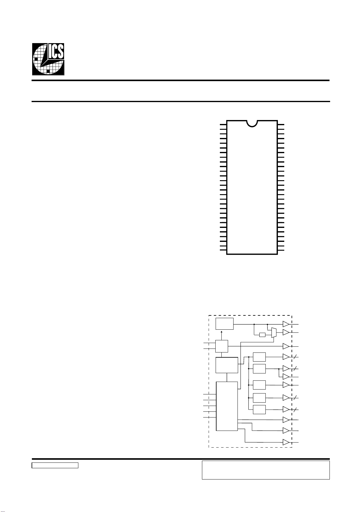
Pin Configuration
Recommended Application:
810/810E and Solano (815) type chipset
Output Features:
• 2 - CPUs @ 2.5V
• 13 - SDRAM @ 3.3V
• 3 - 3V66 @ 3.3V
• 7 - PCI @3.3V
• 1 - 24/48MHz@ 3.3V
• 1 - 48MHz @ 3.3V fixed
• 1 - REF @3.3V, 14.318MHz
Features:
• Programmable ouput frequency
• Gear ratio change detection
• Real time system reset output
• Spread spectrum for EMI control
with programmable spread percentage
• Watchdog timer technology to reset system
if over-clocking causes malfunction.
• Support power management through PD#.
• Uses external 14.318MHz crystal
• FS pins for frequency select
Key Specifications:
• CPU Output Jitter: <250ps
• IOAPIC Output Jitter: <500ps
• 48MHz, 3V66, PCI Output Jitter: <500ps
• CPU Output Skew: <175ps
• PCI Output Skew: <500ps
• 3V66 Output Skew <175ps
• For group skew timing, please refer to the
Group Timing Relationship Table.
Programmable System Frequency Generator for PII/III™
56-Pin 300 mil SSOP
1. These pins will have 1.5 to 2X drive strength.
* 120K ohm pull-up to VDD on indicated inputs.
VDDA
GNDA
X1
X2
GND3V66
VDD3V66
3V66-0
3V66-1
3V66-2
VDDPCI
GNDPCI
*FS0/PCICLK0
*FS1/PCICLK1
*SEL24_48#/PCICLK2
GNDPCI
VDDPCI
PCICLK3
PCICLK4
PCICLK5
PCICLK6
RATIO_0
PD#
SCLK
S DATA
VDD48
GND48
*FS2/24_48MHz
*FS3/48MHz
1
1
1
1
REF/FS4*
VDDLAPIC
IOAPIC0
VDDLCPU
GNDLCPU
CPUCLK0
CPUCLK1
GNDSDR
VDDSDR
SDRAM0
SDRAM1
SDRAM2
SDRAM3
VDDSDR
GNDSDR
SDRAM4
SDRAM5
SDRAM6
SDRAM7
SDRAM_F
GNDSDR
VDDSDR
SDRAM8
SDRAM9
SDRAM10
SDRAM11
RESET#
RATIO_1
1
1
ICS94203
1
2
3
4
5
6
7
8
9
10
11
12
13
14
15
16
17
18
19
20
21
22
23
24
25
26
27
28
56
55
54
53
52
51
50
49
48
47
46
45
44
43
42
41
40
39
38
37
36
35
34
33
32
31
30
29
Block Diagram
PLL2
PLL1
Spread
Spectrum
48MHz
24_48MHz
CPUCLK (1:0)
2
12
7
3
SDRAM (11:0)
IOAPIC
PCICLK (6:0)
SDRAM_F
3V66 (2:0)
RESET#
RATIO_0
RATIO_1
X1
X2
XTAL
OSC
CPU
DIVDER
SDRAM
DIVDER
IOAPIC
DIVDER
PCI
DIVDER
3V66
DIVDER
FS(4:0)
PD#
SEL24_48#
S DATA
SCLK
Control
Logic
Config.
Reg.
/ 2
REF
Power Groups
VDDA, GNDA = Core PLL, Xtal
VDD48, GND48 = 48MHz, Fixed PLL
ICS reserves the right to make changes in the device data identified in
this publication without further notice. ICS advises its customers to
obtain the latest version of all device data to verify that any
information being relied upon by the customer is current and accurate.
2
ICS94203
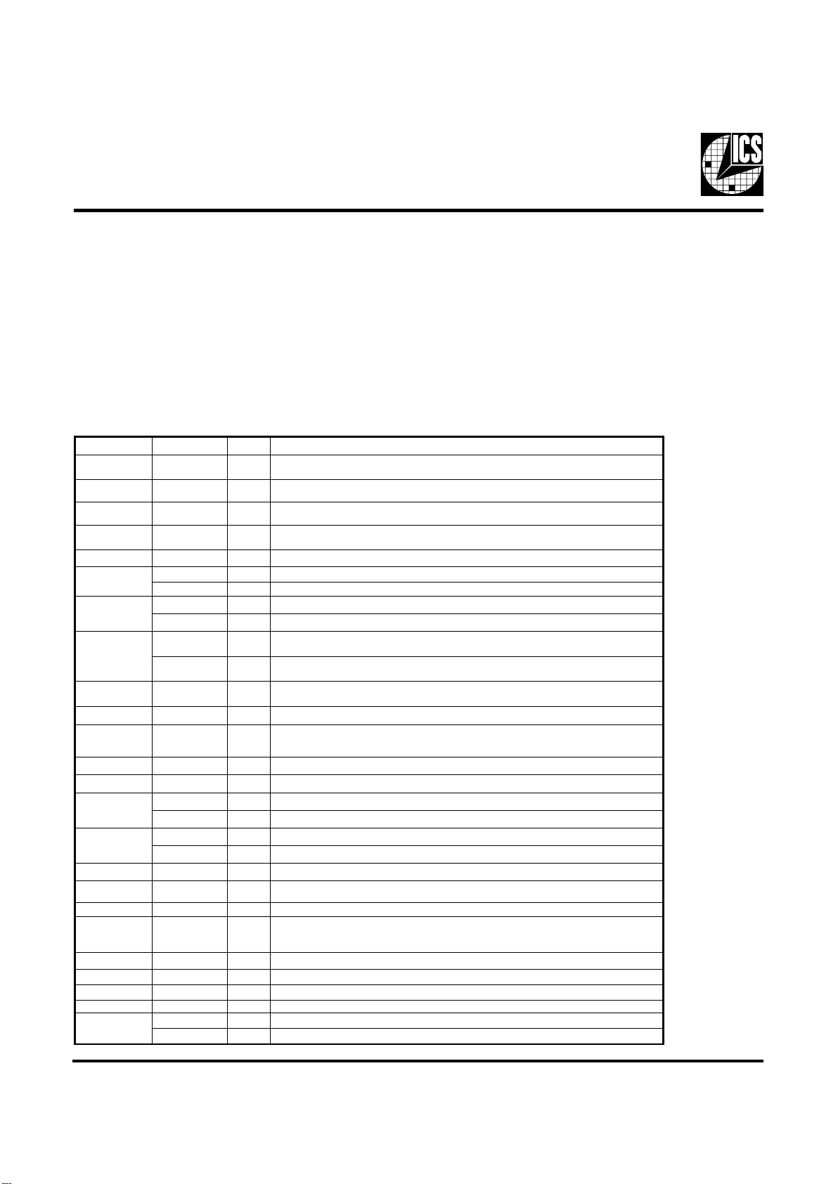
General Description
Pin Configuration
The ICS94203 is a single chip clock solution for desktop designs using the 810/810E and Solano style chipset. It provides all necessary
clock signals for such a system.
The ICS94203 belongs to ICS new generation of programmable system clock generators. It employs serial programming I
2
C interface
as a vehicle for changing output functions, changing output frequency, configuring output strength, configuring output to output skew ,
changing spread spectrum amount, changing group divider ratio and dis/enabling individual clocks. This device also has ICS
propriety 'Watchdog Timer' technology which will reset the frequency to a safe setting if the system become unstable from over
clocking.
Spread spectrum typically reduces system EMI by 7dB to 8dB. This simplifies EMI qualification without resorting to board design
iterations or costly shielding.
REBMUNNIPEMANNIPEPYTNOITPIRCSED
,52,61,01,6,1
84,34,53
DDVRWPylppusrewopV3.3
3
1XNI
kcabdeefdna)Fp33(pacdaollanretnisah,tupnilatsyrC
2Xmorfrotsiser
4
2XTUO)Fp33(pacdaollanretnisaH.zHM813.41yllanimon,tuptuolatsyrC
,62,51,11,5,2
94,24,63
DNGRWPylppusV3.3rofsnipdnuorG
7,8,9
]0:2[66V3TUOBUHrofstuptuokcolczHM66dexiFV3.3
21
0KLCICP
1
TUOSKLCUPCsuonorhcnyShtiw,tuptuokcolcICPV3.3
0SFNI.norewoptadehctaltupnI.tibtcelesycneuqerftupnicigoL
31
1KLCICP
1
TUOSKLCUPCsuonorhcnyShtiw,tuptuokcolcICPV3.3
1SFNI.norewoptadehctaltupnI.tibtcelesycneuqerftupnicigoL
41
#84_42LESNI72niprofniptcelesycneuqerfzHM84/42
2KLCICPTUOSKLCUPCsuonorhcnyShtiw,tuptuokcolcICPV3.3
71,81,91,02
]3:6[KLCICPTUOSKLCUPCsuonorhcnyShtiw,stuptuokcolcICPV3.3
12
0_OITARTUO .rossecorpehtmorfyllanigroslangis0LESBehtgnicalper,tespihcottuptuO
22
#DPNI
ehT.etatsrewopwolaotniecivedehtnwodrewopotdesuniptupniwolevitcasuonorhcnysA
rewopehtfoycnetalehT.deppotseralatsyrcehtdnaOCVehtdnadelbasideraskcolclanretni
.sm3nahtretaergebtonlliwnwod
32
KLCSNIIfotupnikcolC
2
tupniC
42
ATADSO/IIroftupniataD
2
.tupnilairesC
72
2SFNI.norewoptadehctaltupnI.tibtcelesycneuqerftupnicigoL
zHM84_42TUO.zHM42sitluafeDtuptuozHM84_42V3.3
82
3SFNI.norewoptadehctaltupnI.tibtcelesycneuqerftupnicigoL
zHM84TUO.BSUroftuptuokcolczHM84dexiFV3.3
92
1_OITARTUO .rossecorpehtmorfyllanigroslangis1ESBehtgnicalper,tespihcottuptuO
03
TESERTUO
.tuoemitremmitgodhctawroegnahcoitarycneuqerfroflangistesermetsysemitlaeR
.wolevitcasilangissihT
73
F_MARDSTUOIhguorhtffodenrutebnactuptuoMARDSV3.3
2
C
,43,33,23,13
,14,04,93,83
74,64,54,44
]0:11[MARDSTUOIhguorhtffodenrutebnacstuptuoMARDSllA.tuptuoV3.3
2
C
15,05]0:1[KLCUPCTUO.snipSFmorfdeviredycneuqerftuptuO.tuptuokcolcsubtsoHV5.2
25LDNGRWPCIPA&UPCrofylppusrewopV5.2rofdnuorG
55,35LDDVRWPCIPAOI,UPCrofylppyusrewopV5.2
45CIPAOITUO.zHM76.61tagninnurstuptuokcolcV5.2
65
4SFNI.norewoptadehctaltupnI.tibtcelesycneuqerftupnicigoL
FER
1
TUO.tuptuokcolcecnereferzHM813.41,V3.3
3
ICS94203
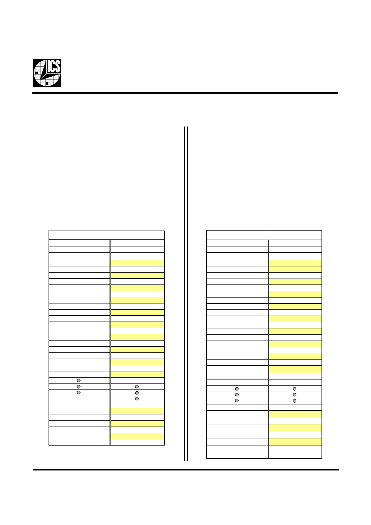
General I2C serial interface information for the ICS94203
How to Write:
• Controller (host) sends a start bit.
• Controller (host) sends the write address D2
(H)
• ICS clock will acknowledge
• Controller (host) sends a dummy command code
• ICS clock will acknowledge
• Controller (host) sends a dummy byte count
• ICS clock will acknowledge
• Controller (host) starts sending Byte 0 through Byte 28
(see Note 2)
• ICS clock will acknowledge each byte one at a time
• Controller (host) sends a Stop bit
How to Read:
• Controller (host) will send start bit.
• Controller (host) sends the read address D3
(H)
• ICS clock will acknowledge
• ICS clock will send the byte count
• Controller (host) acknowledges
• ICS clock sends Byte 0 through byte 6 (default)
• ICS clock sends Byte 0 through byte X (if X
(H)
was
written to byte 6).
• Controller (host) will need to acknowledge each byte
• Controller (host) will send a stop bit
Controll e r (Host)
ICS (Slave/Receiver)
Start Bit
Address D2
(H)
ACK
Dumm y Comm an d Cod e
ACK
Dumm y B y te Count
ACK
Byte 0
ACK
Byte 1
ACK
Byte 2
ACK
Byte 3
ACK
Byte 4
ACK
Byte 5
ACK
Byte 6
ACK
Byte 26
ACK
Byte 27
ACK
Byte 28
ACK
Stop Bit
How to Write:
*See notes on the following page.
Controller (Host)
ICS (Sla ve/Receiver)
Start Bit
Addres s D3
(H)
ACK
Byte Count
ACK
Byte 0
ACK
Byte 1
ACK
Byte 2
ACK
Byte 3
ACK
Byte 4
ACK
Byte 5
ACK
Byte 6
ACK
If 7
H
has been wri t ten to B 6
Byte 7
ACK
If 1A
H
has been wri t ten to B6
Byte26
ACK
If 1B
H
has been wri t ten to B6
Byte 27
ACK
If 1C
H
has been wri t ten to B6
Byte 28
ACK
Stop Bit
How to Read:
4
ICS94203
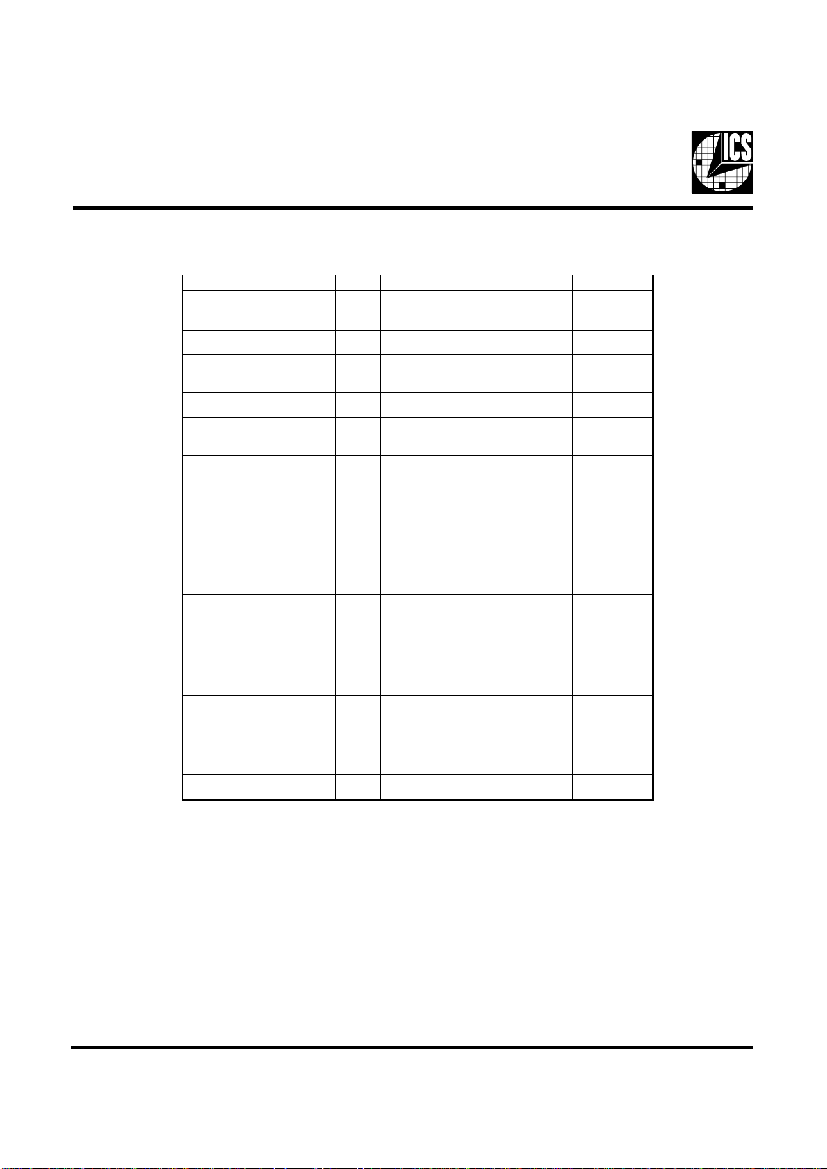
1. The ICS clock generator is a slave/receiver, I2C component. It can read back the data stored in the latches for verification.
Readback will support standard SMBUS controller protocol. The number of bytes to readback is defined by writing to
byte 6.
2. When writing to byte 14 - 15, byte 16 - 17 and byte 18 - 20, they must be written as a set. If for example, only byte
14 is written but not 15, neither byte 14 or 15 will load into the receiver.
3. The data transfer rate supported by this clock generator is 100K bits/sec or less (standard mode)
4. The input is operating at 3.3V logic levels.
5. The data byte format is 8 bit bytes.
6. To simplify the clock generator I
2
C interface, the protocol is set to use only Block-Writes from the controller. The bytes
must be accessed in sequential order from lowest to highest byte with the ability to stop after any complete byte has been
transferred. The Command code and Byte count shown above must be sent, but the data is ignored for those two bytes.
The data is loaded until a Stop sequence is issued.
7. At power-on, all registers are set to a default condition, as shown.
Notes:
Regi s ter Name Byte Descript ion Pwd Default
Functionalit y & Frequency Sel ect
Register
0
Output frequenc y, hardware / I
2
C frequency
select, spread spectrum & output enable
cont rol register.
See individual byt e
description
Output Cont rol Registers 1-5 Active / i nactive output control registers.
See individual byt e
description
By t e Count Read B ac k Register 6
Writ i ng t o t his regist er will c onfigure by t e
count and how m any byt e wi l l be read back.
Do not write 00
H
to this byte.
06
H
Latc hed Input s Read Back
Register
7
The invers e of t he l atched inputs level could
be read back from t his regis ter.
See individual byt e
description
Watchdog Control Regi sters 8 Bit[6:0]
Wat c hd og enable, wat c hdog s t at us and
programmable 'safe' frequency ' c an be
configured in t his regis ter.
000,0000
VCO Control Selection Bit 8 Bit[7]
This bit s el ec t whet her t he out put frequency
is control by hardware/byt e 0 configurations
or byt e 14& 15 program m i ng.
0
Watchdog Timer Count Register 9
Writ i ng t o t his regist er will c onfigure t he
number of seconds for the watchdog t im er
to reset.
FF
H
ICS Reserved Register 10
This is an unus ed regi s t er. W ri t ing to this
regist er wil l no t affect device funct i onal i ty.
00
H
Device ID, Vendor ID & Revision ID
Registers
11-12
By t e 11 bi t[3:0] is ICS vendor id - 0001.
Other bits in these 2 regis ters des i gnate
device revision ID of this part .
See individual byt e
description
ICS Reserved Register 13
Don't write int o this register, writing 1's will
caus e m al function.
00
H
VCO Frequenc y Control Registers 14-15
These registers control the di viders rat io
into t he phase detec tor and thus control t he
VCO outpu t frequenc y.
Depended on
hardware/byte 0
configuration
Spread Spec t rum Cont rol
Registers
16-17
These registers control the spread
percentage am ount.
Depended on
hardware/byte 0
configuration
Output Di viders Cont rol Regi sters 18-20
Changing bits i n t hes e registers res ul t in
frequency di vider ratio changes. Inc orrec t
configuration of group output divider ratio
can cause system malfunction.
Depended on
hardware/byte 0
configuration
Group Sk ews Control Regis ters 21
Increment or dec rem ent t he group s k ew
amount as compared to the initial s kew.
See individual byt e
description
Output Ri se/Fall Tim e S elect
Registers
22
These register will control the group rise
and fall ti m e.
See individual byt e
description
Brief I2C registers description for ICS94203
Programmable System Frequency Generator
5
ICS94203
Byte 0: Functionality and frequency select register (Default=0)
Notes:
1.
Default at power-up will be for latched logic inputs to define frequency, as displayed by Bit 3.
tiB
noitpircseD
DWP
tiB
)4:7,2(
2tiB7tiB6tiB5tiB4tiB
FER/OCV
rediviD
OCV
zHM
/OCV
UPC
KLCUPC
zHM
MARDS
zHM
66V3
zHM
KLCICP
zHM
CIPAOI
zHM
1etoN
4SF3SF2SF1SF0SF
00000 31/26317.893654.6656.9934.6612.3316.61
00001 41/25300.063600.0600.0900.0600.0300.51
00010 81/40519.004608.6602.00108.6604.3307.61
00011 11/51320.014633.8605.20133.8671.4380.71
00100 51/04400.024600.0700.50100.0700.5305.71
00101 41/04400.054600.5705.21100.5705.7357.81
00110 51/30541.084600.0800.02100.0800.0400.02
00111 9/31359.794600.3805.42100.3805.1457.02
01000 73/51592.991256.9956.9934.6612.3316.61
01001 04/74492.061200.0800.0833.3576.6233.31
01010 73/81554.0022 32.00132.00148.6614.3307.61
01011 13/64400.6022 00.30100.30176.8633.4371.71
01100 33/48400.0122 00.50100.50100.0700.5305.71
01101 33/70589.9122 00.01100.01133.3776.6333.81
01110 23/41599.9222 00.51100.51176.6733.8371.91
01111 11/16460.0062 00.00200.00200.00100.0500.52
10000 31/26317.8933 68.23168.23134.6612.3316.61
10001 51/30541.0843 00.06100.06100.0800.0400.02
10010 81/40519.0043 46.33146.33128.6614.3307.61
10011 71/88420.1143 00.73100.73105.8652.4331.71
10100 51/04400.0243 00.04100.04100.0700.5305.71
10101 31/59350.5343 00.54100.54105.2752.6331.81
10110 41/04400.0543 00.05100.05100.5705.7357.81
10111 51/30541.0843 00.06100.06100.0800.0400.02
11000 31/26317.8933 09.23156.9939.6612.3316.61
11001 51/30541.0843 00.06100.00100.0800.0400.02
11010 81/40519.0043 46.33132.00128.6614.337.61
11011 71/88420.1143 00.73157.20105.8652.4331.71
11100 51/04400.0243 00.04100.50100.0700.5305.71
11101 31/59350.5343 00.54157.80105.2752.6331.81
11110 41/04400.0543 00.05105.21100.5705.7357.81
11111 51/30541.0843 00.06100.02100.0800.0400.02
3tiB
stupnidehctal,tceleserawdrahybdetcelessiycneuqerF-0
4:7,2tiBybdetcelessiycneuqerF-1
0
1tiB
lamroN-0
daerpSretneC%53.0±elbanemurtcepsdaerpS-1
1
0tiB
gninnuR-0
stuptuollaetatsirT-1
0
6
ICS94203
Notes:
1. Inactive means outputs are held LOW and are disabled from switching. These outputs are designed to be configured at
power-on and are not expected to be configured during the normal modes of operation.
2. PWD = Power on Default
Byte 1: Output Control Register
(1 = enable, 0 = disable)
Notes:
1. Inactive means outputs are held LOW and are disabled from switching. These outputs are designed to be configured at
power-on and are not expected to be configured during the normal modes of operation.
2. PWD = Power on Default
Byte 3: Output Control Register
(1 = enable, 0 = disable)
Byte 2: Output Control Register
(1 = enable, 0 = disable)
Byte 4: Output Control Register
(1 = enable, 0 = disable)
Byte 5: Output Control Register
(1 = enable, 0 = disable)
Byte 6: Byte Count Read Back Register
Note: Writing to this register will configure byte count and
how many bytes will be read back, default is 6 bytes.
tiB#niPDWPnoitpircseD
7tiB831 7MARDS
6tiB931 6MARDS
5tiB041 5MARDS
4tiB141 4MARDS
3tiB441 3MARDS
2tiB541 2MARDS
1tiB641 1MARDS
0tiB741 0MARDS
tiB#niPDWPnoitpircseD
7tiB91 2_66V3
6tiB71 0_66V3
5tiB81 1_66V3
4tiB651FER
3tiB451 0CIPAOI
2tiB-X devreseR
1tiB051 1KLCUPC
0tiB151 0KLCUPC
tiB#niPDWPnoitpircseD
7tiB-0 )etoN(devreseR
6tiB-0 )etoN(devreseR
5tiB-0 )etoN(devreseR
4tiB-0 )etoN(devreseR
3tiB-0 )etoN(devreseR
2tiB-1 )etoN(devreseR
1tiB-1 )etoN(devreseR
0tiB-0 )etoN(devreseR
tiB#niPDWPnoitpircseD
7tiB-1 )devreseR(
6tiB-1 )devreseR(
5tiB-1 )devreseR(
4tiB-1 )devreseR(
3tiB131 11MARDS
2tiB231 01MARDS
1tiB331 9MARDS
0tiB431 8MARDS
tiB#niPDWPnoitpircseD
7tiB-0 devreseR
6tiB021 6KLCICP
5tiB911 5KLCICP
4tiB811 4KLCICP
3tiB711 3KLCICP
2tiB411 2KLCICP
1tiB311 1KLCICP
0tiB211 0KLCICP
tiB#niPDWPnoitpircseD
7tiB
-1 )devreseR(
6tiB
-1 )devreseR(
5tiB
-1 )devreseR(
4tiB
721 zHM84_42
3tiB
-1 )devreseR(
2tiB
821 zHM84
1tiB
-1 )devreseR(
0tiB
731 F_MARDS
 Loading...