

查询HMC280MS8G供应商
MICROWAVE CORPORATION
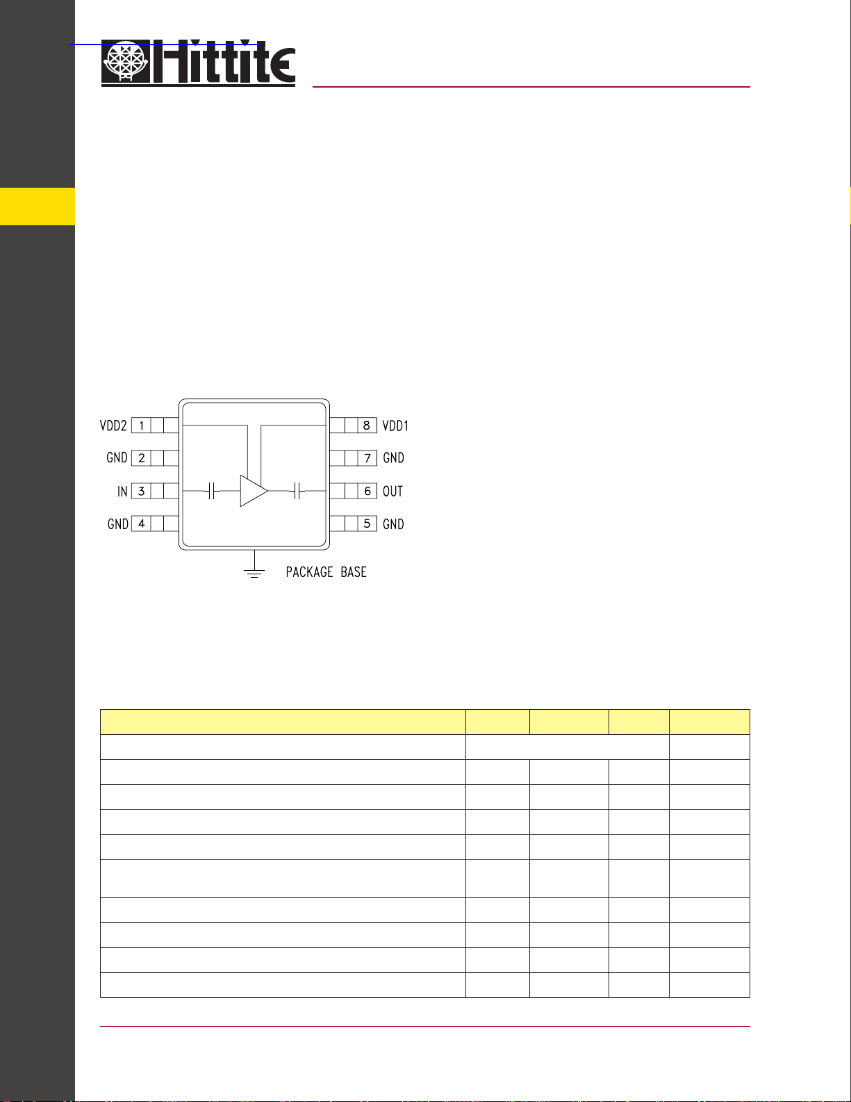
Typical Applications
8
The HMC280MS8G is ideal for:
• UNII & HiperLAN
• ISM
Functional Diagram
AMPLIFIERS - SMT
v03.0703
HMC280MS8G
GaAs MMIC POWER AMPLIFIER
5.0 - 6.0 GHz
Features
Psat Output Power: +24 dBm
Output IP3: +38 dBm
High Gain: 18 dB
Single Supply: +3.6V
Ultra Small Package: MSOP8G
General Description
The HMC280MS8G is a +3.6V GaAs MMIC power
amplifi er covering 5 to 6 GHz. The device is packaged in a low cost, surface mount 8 lead MSOP
plastic package with an exposed base paddle for
improved RF ground and thermal dissipation. The
amplifi er provides 18 dB of gain and 24 dBm
Psat while operating from a single positive supply.
External component requirements are minimal
with the amplifi er occupying less than 0.023 sq.
in. (14.6 sq. mm). All data is taken with the
amplifi er assembled into a 50 ohm test fi xture
with the exposed base paddle connected to RF
ground. For transmit / receive applications use
with either the HMC223MS8 or HMC224MS8
SPDT switches.
8 - 8
Electrical Specifi cations, T
Parameter Min. Typ. Max. Units
Frequency Range 5.0 - 6.0 GHz
Gain 14 19 23 dB
Gain Flatness ±1.0 dB
Input Return Loss 8 12 dB
Reverse Isolation 40 44 dB
Output Power for 1 dB Compression (P1dB)
Saturated Output Power (Psat) 21 24 dBm
Output Third Order Intercept (IP3) 33 38 dBm
Noise Figure 13 dB
Supply Current (Idd)(Vdd1 = Vdd2 = +3.6 Vdc) 480 mA
For price, delivery, and to place orders, please contact Hittite Microwave Corporation:
12 Elizabeth Drive, Chelmsford, MA 01824 Phone: 978-250-3343 Fax: 978-250-3373
= +25° C, Vdd= +3.6V
A
5.0 - 5.5 Ghz
5.0 - 6.0 Ghz
Order Online at www.hittite.com
20
18
23
22
dBm
MICROWAVE CORPORATION
v03.0703
HMC280MS8G
GaAs MMIC POWER AMPLIFIER
5.0 - 6.0 GHz
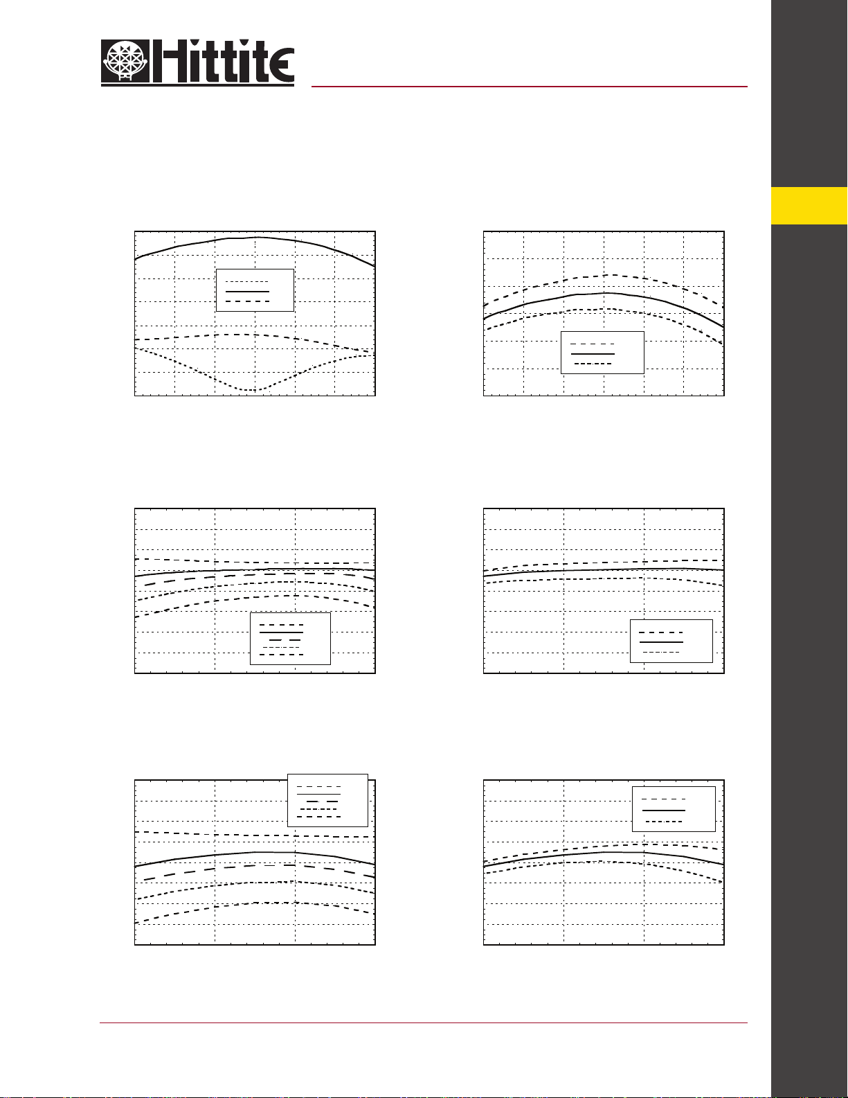
Broadband Gain & Return Loss Gain vs. Temperature @ 3.6V
20
15
10
5
0
RESPONSE (dB)
-5
-10
-15
4 4.5 5 5.5 6 6.5 7
FREQUENCY (GHz)
S11
S21
S22
Psat vs. Supply Voltage Psat vs. Temperature @ 3.6V
30
28
26
24
22
20
18
OUTPUT PSAT (dBm)
16
14
4.5 5 5.5 6
FREQUENCY (GHz)
5V
3.6V
3.3V
3V
2.7V
30
25
20
15
GAIN (dB)
10
5
0
4 4.5 5 5.5 6 6.5 7
FREQUENCY (GHz)
30
28
26
24
22
20
18
OUTPUT PSAT (dBm)
16
14
4.5 5 5.5 6
FREQUENCY (GHz)
-40C
+25C
+70C
-40C
+25C
+70C
8
AMPLIFIERS - SMT
P1dB vs. Supply Voltage P1dB vs. Temperature @ 3.6V
30
28
26
24
22
20
18
OUTPUT P1dB (dBm)
16
14
4.5 5 5.5 6
FREQUENCY (GHz)
For price, delivery, and to place orders, please contact Hittite Microwave Corporation:
12 Elizabeth Drive, Chelmsford, MA 01824 Phone: 978-250-3343 Fax: 978-250-3373
Order Online at www.hittite.com
5V
3.6V
3.3V
3V
2.7V
30
28
26
24
22
20
18
OUTPUT P1dB (dBm)
16
14
4.5 5 5.5 6
FREQUENCY (GHz)
-40C
+25C
+70C
8 - 9

MICROWAVE CORPORATION
v03.0703
HMC280MS8G
GaAs MMIC POWER AMPLIFIER
Power Compression @ 5.25 GHz Output IP3 vs Supply Voltage @ 6.0 GHz
8
30
25
20
15
10
5
Pout (dBm), GAIN (dB), PAE (%)
0
-10 -5 0 5 10 15
Output Power (dBm)
Gain (dB)
PAE (%)
INPUT POWER (dBm)
Output IP3 vs. Temperature @ 3.6V
AMPLIFIERS - SMT
50
45
5.0 - 6.0 GHz
50
45
40
35
OIP3 (dBm)
30
25
20
2.5 3 3.5 4 4.5 5 5.5
Vdd SUPPLY VOLTAGE (Vdc)
Output IP3 vs. Temperature @ 5.0V
50
45
-40C
+25C
+70C
40
35
OIP3 (dBm)
30
25
20
4.5 5 5.5 6
FREQUENCY (GHz)
0
-10
-20
-30
-40
-50
REVERSE ISOLATION (dB)
-60
4.5 5 5.5 6
40
35
OIP3 (dBm)
-40C
+25C
+70C
30
25
20
4.5 5 5.5 6
Reverse Isolation @ 3.6V
FREQUENCY (GHz)
FREQUENCY (GHz)
-40C
+25C
+70C
8 - 10
For price, delivery, and to place orders, please contact Hittite Microwave Corporation:
12 Elizabeth Drive, Chelmsford, MA 01824 Phone: 978-250-3343 Fax: 978-250-3373
Order Online at www.hittite.com

MICROWAVE CORPORATION
v03.0703
HMC280MS8G
GaAs MMIC POWER AMPLIFIER
Absolute Maximum Ratings
Drain Bias Voltage (Vdd1, Vdd2) +8.0 Vdc
RF Input Power (RFin) (Vdd = +3.6 Vdc) +20 dBm
Channel Temperature 150 °C
Continuous Pdiss (T = 85 °C)
(derate 41 mW/°C above 85 °C)
Thermal Resistance
(channel to ground paddle )
Storage Temperature -65 to +150 °C
Operating Temperature -55 to +85 °C
2.67 W
24.3 °C/W
Outline Drawing
5.0 - 6.0 GHz
8
AMPLIFIERS - SMT
NOTES:
1. PACKAGE BODY MATERIAL: LOW STRESS INJECTION MOLDED
PLASTIC SILICA AND SILICON IMPREGNATED.
2. LEADFRAME MATERIAL: COPPER ALLOY
3. LEADFRAME PLATING: Sn/Pb SOLDER
4. DIMENSIONS ARE IN INCHES [MILLIMETERS].
5. DIMENSION DOES NOT INCLUDE MOLDFLASH OF 0.15mm PER SIDE.
6. DIMENSION DOES NOT INCLUDE MOLDFLASH OF 0.25mm PER SIDE.
7. ALL GROUND LEADS AND GROUND PADDLE MUST BE SOLDERED
TO PCB RF GROUND.
For price, delivery, and to place orders, please contact Hittite Microwave Corporation:
12 Elizabeth Drive, Chelmsford, MA 01824 Phone: 978-250-3343 Fax: 978-250-3373
Order Online at www.hittite.com
8 - 11

MICROWAVE CORPORATION
v03.0703
HMC280MS8G
GaAs MMIC POWER AMPLIFIER
Recommended PCB Layout
8
AMPLIFIERS - SMT
5.0 - 6.0 GHz
8 - 12
List of Material
Item Description
J1, J2 PC Mount SMA Connector
J3, J4, J5 DC Pins
C1, C2 1000 pF Capacitor, 0603 Pkg.
C3, C4 100 pF Capacitor, 0402 Pkg.
L1 3.9 nH Inductor, 0402 Pkg.
U1 HMC280MS8G Amplifi er
PCB* 103104 Evaluation Board
*Circuit Board Material: Roger 4350
For price, delivery, and to place orders, please contact Hittite Microwave Corporation:
12 Elizabeth Drive, Chelmsford, MA 01824 Phone: 978-250-3343 Fax: 978-250-3373
The circuit board used in the fi nal application should
use RF circuit design techniques. Signal lines should
have 50 ohm impedance while the package ground
leads and exposed paddle should be connected directly
to the ground plane similar to that shown. A suffi cient
number of via holes should be used to connect the top
and bottom ground planes. The evaluation circuit board
shown is available from Hittite upon request.
Order Online at www.hittite.com

MICROWAVE CORPORATION
v03.0703
HMC280MS8G
GaAs MMIC POWER AMPLIFIER
Application Circuit
5.0 - 6.0 GHz
8
AMPLIFIERS - SMT
Note 1: Vdd1 and Vdd2 may be connected to a common Vdd feed after RF choke.
Recommended Component Values
L1 3.9 nH
C1 1000 pF
C2 100 pF
Note 2: L1 should be located < 0.020” (0.508 mm) from pin 8 (Vdd1).
For price, delivery, and to place orders, please contact Hittite Microwave Corporation:
12 Elizabeth Drive, Chelmsford, MA 01824 Phone: 978-250-3343 Fax: 978-250-3373
Order Online at www.hittite.com
8 - 13
 Loading...