

Page 1
N
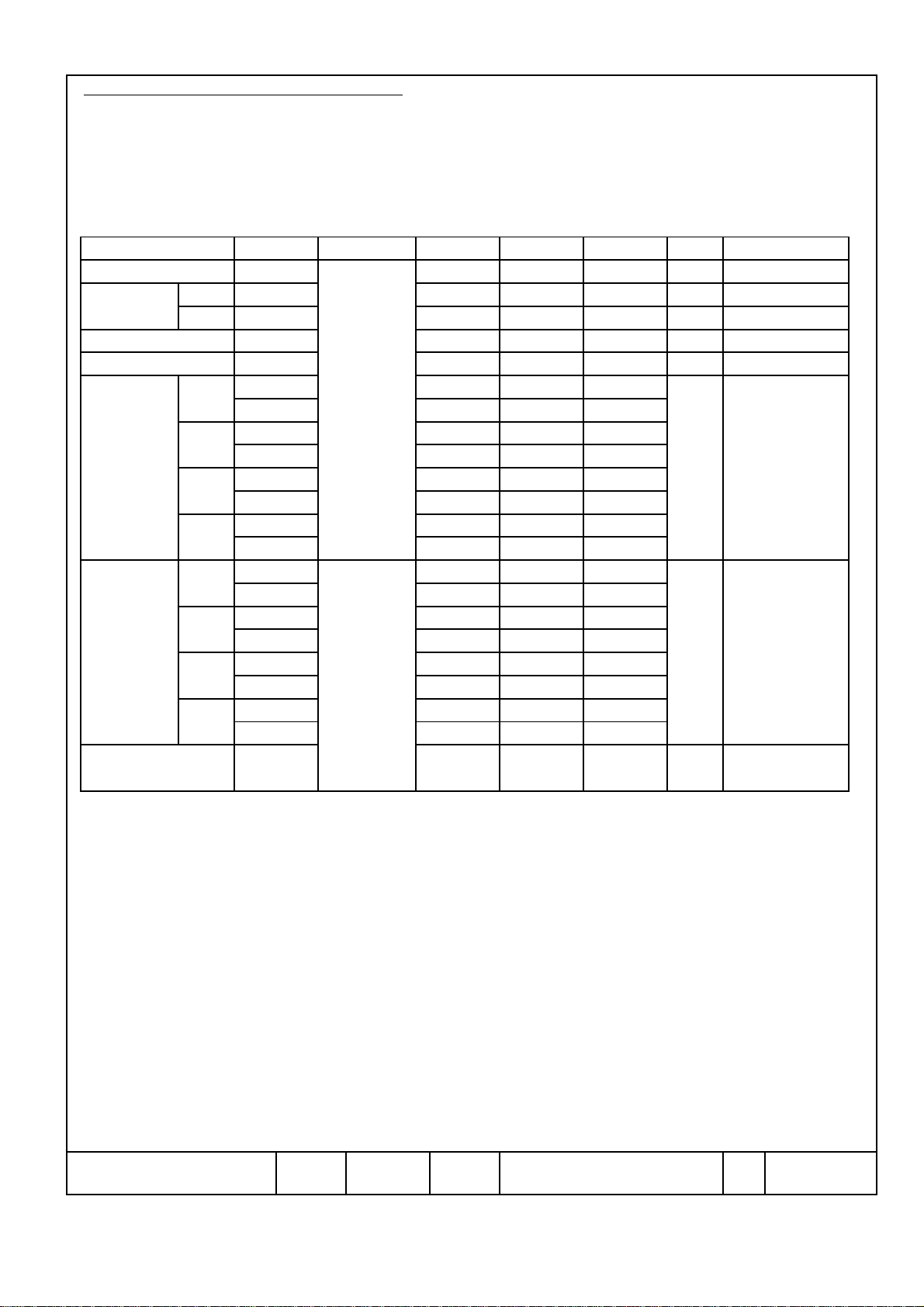
TECHNICAL DATA
AX094F002F
AX094F002B
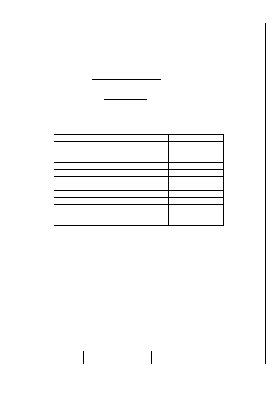
CONTENTS
No. Item Page
- COVER 1-1/1
- RECORD OF REVISION 2-1/1
- DESCRIPTION 3-1/1
1 ABSOLUTE MAXIMUM RATINGS 4-1/1
2 INITIAL OPTICAL CHARACTERISTICS 5-1/2~2/2
3 ELECTRICAL CHARACTERISTICS 6-1/2~2/2
4 BLOCK DIAGRAM 7-1/1
5 INTERFACE PIN ASSIGNMENT 8-1/7~7/7
6 INTERFACE TIMING 9-1/3~3/3
Date:Mar. 29, 2007
STD-2700-1
IPS Alpha Technology,Ltd.
Date
Mar. 29, 2007
Sheet
o.
STD2700-1
Page
1-1/1
Page 2
Date
N
RECORD OF REVISION
The upper section : Before revision
The lower section : After revision
Sheet No.
Page
Summary
IPS Alpha Technology,Ltd.
Date
Mar. 29, 2007
Sheet
o.
STD2700-1
Page
2-1/1
Page 3
N
DESCRIPTION
N
AX094F002F
The following specifications are applied to the following IPS-Pro module.
ote : Inverter for back light unit is built in this module.
Product Name : AX094F002B
General Specifications
Effective Display Area :(H)819.36(V)460.89 (mm)
Number of Pixels :(H)1,920×(V)1,080 (pixels)
Pixel Pitch :(H)0.42675×(V)0.42675 (mm)
Color Pixel Arrangement : R+G+B Vertical Stripe
Display Mode : Transmissive Mode
Normally Black Mode
Top Polarizer Type : Anti-Glare
Number of Colors :16,777,216 (colors)
Viewing Angle Range : Super Wide Version
(Horizontal & Vertical : 178°, CR≧10)
Input Signal : 2-channel LVDS (LVDS:Low Voltage Differential Signaling)
Back Light : 20 pcs. of EEFL
External Dimensions : (H)877 x (V)516.8 x (t)55.5 (mm)
Weight :Typ 9,500 (g)
IPS Alpha Technology,Ltd.
Date
Mar. 29, 2007
Sheet
o.
STD2700-1
Page
3-1/1
Page 4
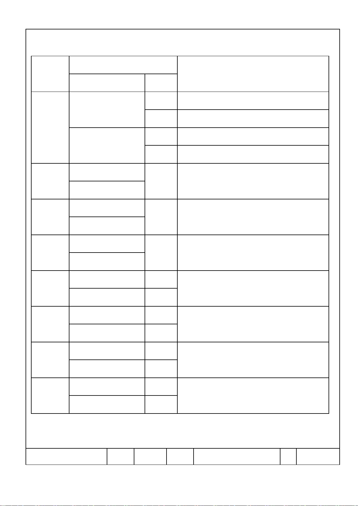
1. ABSOLUTE MAXIMUM RATINGS
N
1.1 Environmental Absolute Maximum Ratings
ITEM
Operating
Min. Max. Min. Max.
Temperature 0 50 -20 60
Humidity 2)
Vibration - 4.9(0.5G) - 14.7(1.5G)
Shock - 29.4(3G)
Corrosive Gas Not Acceptable Not Acceptable -
Illumination at
LCD Surface
- 50,000
Note 1) Temperature and Humidity should be applied to the glass surface of a Super-TFT module,
not to the system installed with a module.
The temperature at the center of rear surface should be less than 70℃ on the condition of operating.
The brightness of a EEFL tends to drop at low temperature. Besides, the life-time becomes shorter
at low temperature.
2) Ta≦40 ℃‥‥‥Relative humidity should be less than 85%RH max. Dew is prohibited.
Ta>40 ℃‥‥‥Relative humidity should be lower than the moisture of the 85%RH at 40℃.
3) Frequency of the vibration is between 15Hz and 100Hz. (Remove the resonance point)
4) Pulse width of the shock is 10 ms.
5) Long operation under low temperature may cause some portion of display area to be reddish for
several minutes after turning on the product.
However, it does not affect the characteristics and reliability of the product.
Storage
2)
-
294(30G)
- 50,000 1x
Unit
℃
%RH
m/s
m/s
Note
1),5)
1)
2
2
3)
4)
1.2 Electrical Absolute Maximum Ratings
(1)TFT Module Vss = 0 V
ITEM SYMBOL Min.
Power Supply Voltage
Input Voltage for logic
Electrostatic Durability
V
DD
1
V
ESD0
V
VESD1
Max.
0
-0.3
13.2
3.6 V
±100 V 2),3)
±8
Unit
Note
V
1)
kV 2),4)
Note 1)It is applied to pixel data signal and clock signal.
2)Discharge Coefficient:200pF-250Ω, Environmental:25℃-70%RH
3)It is applied to I/F connector pins.
4)It is applied to the surface of a metallic bezel and a LCD panel.
(2) Back-light Inverter Vss = 0 V
ITEM
Input Voltage
ON/OFF Control Input Voltage
Brightness Control Voltage
SYMBOL Min. Max.
Vin 0 28.0 V
5.5ON/OFF -0.3
BRT -0.3 5.5 V
Unit Note
V
VError Signal Control ERR -0.3 5.5
IPS Alpha Technology,Ltd.
Date
Mar. 29, 2007
Sheet
o.
STD2700-1
Page
4-1/1
Page 5
2. INITIAL OPTICAL CHARACTERISTICS
N
The following optical characteristics are measured under stable conditions. It takes about 30 minutes
to reach stable conditions. The measuring point is the center of display area unless otherwise noted.
The optical characteristics should be measured in a dark room or equivalent state.
Measuring equipment:CS-1000A, or equivalent
Ambient Temperature =25℃、VDD=12.0V、f V=60Hz、
Vin=24V、 BRT=3.3V
Typ. Max. UNIT NOTEITEM SYMBOL CONDITION Min.
Contrast Ratio
Response Time
Brightness of white Bwh 350 (500)
Brightness uniformity Buni - - 30
Color
Chromaticity
(CIE)
Variation of
Color Position
(CIE)
Contrast Ratio at 89° CR89 10
Rise ton - 8 20 ms 3)
Fall toff - 6 20 ms 3)
Red
Green
Blue
White
Red
Green
Blue
White
CR
χ 0.62
y
χ 1) 0.27 0.30
y
χ 0.12 0.15 0.18
y
χ 0.243 0.273
y
∆χ - - 0.04
∆χ - - 0.04
∆y - - 0.04
∆χ - - 0.04
∆y --
∆χ - - 0.04
∆y --
θ=0° 0.30 0.33 0.36
θ=+50°
φ=0°、90°
180°、270°
1)
600 (900) -- 2)
-
0.65 0.68
0.33
0.59
0.04 0.065 0.10
0.245 0.275 0.305
0.62 0.65
0.303
0.04
0.04
---
cd/m
%
-
-
2
4)
【Gray scale
=255】
5)∆y - - 0.04
【Gray scale
=255】
Estimated value
IPS Alpha Technology,Ltd.
Date
Mar. 29, 2007
Sheet
o.
STD2700-1
Page
5-1/2
Page 6
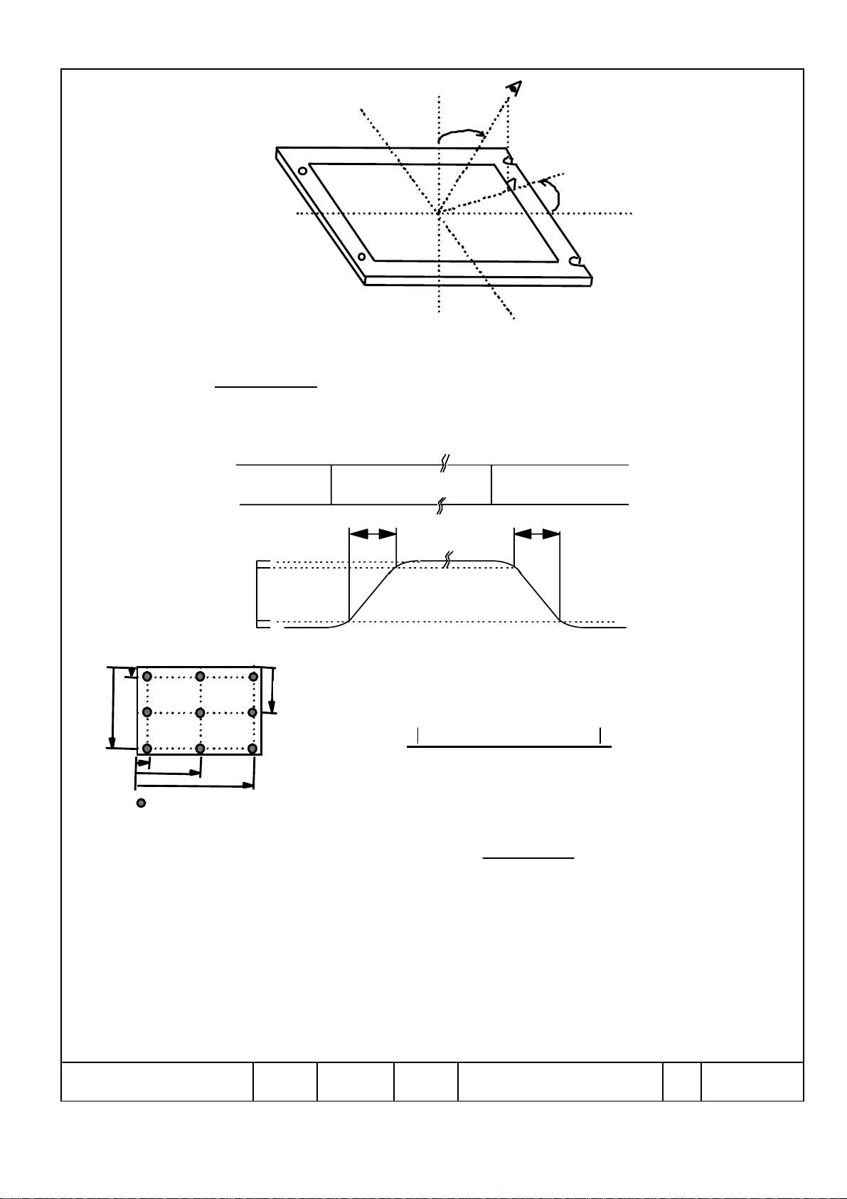
Note 1) Definition of Viewing Angle
t
N
(12 o'clock)
φ=180°
X'
(9 o'clock)
φ=90°
Y
TFT - LCM
θ=0°
Z
θ
eye
φ
φ=0°
X(3o'clock)
2) Definition of Contrast Ratio (CR)
(Luminance at displaying WHITE)
CR=
(Luminance at displaying BLACK)
3) Definition of Response Time
Displaying
Data Signal
Optical
Response
( Luminance)
4) Definition of Brightness Uniformi
10%
(1) (2) (3)
90%
(4) (5) (6)
(7)
10%
:measuring points
(8) (9)
50%
%
100
90
10
BLACK
0
50%
90%
Z'
φ=270°
Y'
(6 o'clock)
WHITE
ton toff
Display pattern is white (255 level) . The brightness
uniformity is defined as the following equation. Brightness at each
point is measured, and average, maximum and minimum
brightness is calculated.
Buni=
where, Bmax = Maximum brightness
Bmin = Minimum brightness
Bmax or Bmin - Bave
Bave
BLACK
×100
9
Σ (B(k))
Bave =Average brightness=
k=1
9
5)Variation of color position on CIE is defined as difference between colors at θ=0°and
atθ=50°& φ=0°90°180°270°.
Date
IPS Alpha Technology,Ltd.
Mar. 29, 2007
Sheet
o.
STD2700-1
Page
5-2/2
Page 7

3. ELECTRICAL CHARACTERISTICS
N
3.1 TFT-LCD Module Ta=25℃、Vss=0V
SYSTEM
Power supply Voltage
Power supply Current
Ripple voltage of power Supply
LVDS select
Note 1)fV=60.0Hz,fCLK=66MHz,VDD=12.0V,and Display pattern is white.
High
Low
DD
V
I
DD
DDR
V
LVDSSEL
Min.
11.4
-
- 150 mV
2.2 2.5
0 0 0.6
TypITEM
12.0 12.6
0.9 1.25
-
Max
3.6
単位
TFT Module
DC Ampere Meter
V
DD
V
SS
2) Current fuse is built in a module. Current capacity of power supply for VDD
should be larger than 4A, so that the fuse can be opened at the trouble of electrical circuit of module.
V
A
V
V
備考
1),2)
3.2 Back Light
Symbol Min. Typ. Max. Unit
21.6 24.0 26.4 VInput Voltage VBL
Input Current
ON/OFF
Control Voltage
Brigthness Control
Input Voltage
Output frequency f 54.5
Error Signal Control
Note 3)This characteristics should be applied putting on the lamp about 60 minutes later
with ambient temperature. (Ta=25℃±2℃)
Min. Brightness
Max. Brightness
Normal
Abnormal
IBL (5.2)
ON/OFF
BRT
ERR
-
2.2
-0.3OFF
-
3.0
Open Collector
6.5
-ON
-
0
- 3.3 V
57.0
0 0.8 V-
5.5 V
0.8
-
59.5 kHz
A
V
V
V
NotesITEM
VBL=24V,
BRT=3.3V,3)
IPS Alpha Technology,Ltd.
Date
Mar. 29, 2007
Sheet
o.
STD2700-1
Page
6-1/1
Page 8

4. BLOCK DIAGRAM
N
(1) Super-TFT Module
SourceDriver
2ch-LVDS
Display data.
Timing signal.
DC Power supply
(2) Back light unit
DC
power supply
ON/OFF
Control
Brightness
Control
CN2
CN1
LVDS
Receiver
Back light
Inverter
Tcon
Timing
Converter
DC/DC
Converter
Synchronized Signal
Lamp 20
G1
G2
Gate Driver
G1080
D1 D2 D5760
G1
G2
TFT-LCD
Gate Driver
G1080
CN3
DC power supply
Back light
Inverter
(Master)
ERROR
IPS Alpha Technology,Ltd.
Date
Mar. 29, 2007
Lamp 2
Lamp 1
Sheet
o.
(Slave)
STD2700-1
Page
7-1/1
Page 9

5. INTERFACE PIN ASSIGNMENT
L
N
5. 1 TFT-LCD MODULE
CN1:JAE FI-R51S-HF
(Matching connector : JAE FI-R51-HL)
PIN
SYMBOL
No. No.
1 VSS 28GND(0V)
2 IC 29 RxB0+
3IC
IC
4
IC
5
6IC
VDSSE
7
8IC
9IC 36
10 IC
11 VSS
12 RxA0-
13 RxA0+
14 RxA1-
15 RxA1+
16 RxA2-
17 RxA2+
18 VSS
19 CLKA-
20
CLKA+
21 VSS
22 RxA3-
23 RxA3+
24 IC
25 IC
26
VSS
27 VSS
Description
Internally Connected ,
Keep Open
Select LVDS Data Format
Internally Connected,
Keep Open
GND(0V)
ODD Pixel Data
ODD Pixel Data
ODD Pixel Data
GND(0V)
ODD Pixel Clock
GND(0V)
ODD Pixel Data
Internally Connected,
Keep Open
GND(0V)
2)
3)
3)
3)
2)
3)
2)
3)
2)
PIN
SYMBOL
RxB0-
30
RxB1-
RxB1+
31
32
RxB2-
33
RxB2+
34
CLKB-35
CLKB+
37
382)
RxB3-
39
RxB3+
40
41 IC
42
43
44 VSS
45 VSS
46
47
48 VDD
49 VDD
50
51 VDD
VSS
VSS
IC
VSS
VSS
VSS
NC
VDD
DescriptionNote
EVEN Pixel Data
EVEN Pixel Data
EVEN Pixel Data
GND(0V)
EVEN Pixel Clock
GND(0V)
EVEN Pixel Data
Internally Connected,
Keep Open
No Connection
Power Supply (typ.+12V)
Note
3)
3)
3)
2)
3)
2)
3)
2)GND(0V)
1)
Notes 1) All VDD pins shall be connected to +12.0V(Typ.).
2) All VSS pins shall be grounded. Metal bezel is internally connected to VSS.
3) Rx n+ and Rx n- (n=0,1,2,3) should be wired by twist-pairs or side-by-side FPC patterns, respectively.
IPS Alpha Technology,Ltd.
Date
Mar. 29, 2007
Sheet
o.
STD2700-1
Page
6-1/7
Page 10

5. 2 BACK-LIGHT UNIT
N
N
N
CN2:JST S14B-PH-SM3-TF(LF)
(Matching connecor : JST PHR-14)
Pin No. Description Note
1
2
3 1)
4
5
6
7
8
9
10
11
12
13 BRT
14 IC
otes 1) All VIN pins shall be connected to +24.0V(Typ.).
2) All VSS pins shall be grounded. Metal bezel is internally connected to VSS.
SYMBOL
VIN
VIN
VIN
VIN
VIN
VSS
VSS
VSS
VSS
VSS
ERR
ON/OFF
Power Supply (typ.+24.0V)
GND(0V)
Error Signal Control
High:Lamp ON, Low:Lamp OFF
Brightness Control
Internally Connected, Keep Open
2)
CN3:JST S12B-PH-SM3-TF(LF)
(Matching connecor : JST PHR-12)
Pin No. Description
1 VIN
2 VIN
3 VIN 1)
4 VIN
5 VIN
6 VSS
7 VSS
8 VSS
9 VSS
10 VSS
11 NC
12 NC
otes 1) All VIN pins shall be connected to +24.0V(Typ.).
2) All VSS pins shall be grounded. Metal bezel is internally connected to VSS.
SYMBOL
Power Supply (typ.+24.0V)
GND(0V)
NC
NC
Note
2)
IPS Alpha Technology,Ltd.
Date
Mar. 29, 2007
Sheet
o.
STD2700-1
Page
8-2/7
Page 11

5.3 BLOCK DIAGRAM OF INTERFACE
7
7
7
N
N
R
CN1
RA0-RA7
GA0-GA7
BA0-BA7
VSYNC
HSYNC
DE
DCLK
RB0-RB7
GB0-GB7
BB0-BB7
RSVD1)
RSVD1)
RSVD1)
DCLK
Host
Graphics
Controller
TV set Side
TxIN
PLL
PLL
TFT-LCD Module Side
RxA 0+
RxA 0RxA 1+
RxA 1RxA 2+
RxA 2-
RxA 3+
RxA 3-
100Ω
100Ω
100Ω
100Ω
TTL Parallel-to-LVDS
CLKA+
CLKA-
RxB 0+
RxB 0RxB 1+
RxB 1RxB 2+
RxB 2-
RxB 3+
RxB 3-
100Ω
100Ω
100Ω
100Ω
100Ω
PLL
TTL Parallel-to-LVDS
CLKB+
CLKB-
100Ω
Timing Converter
PLL
xOUT
RA0-RA7
GA0-GA7
BA0-BA7
not connect
not connect
DE
DCLK
RB0-RB7
GB0-GB7
BB0-BB7
not connect
not connect
not connect
LVDS-to-LVDS Parallel LVDS-to-LVDS Parallel
DCLK
RA0~RA7, RB0~RB
GA0~GA7, RB0~RB
BA0~BA7,BB0~BB
:Pixel R Data
:Pixel G Data
:Pixel B Data
(7; MSB, 0; LSB)
(7; MSB, 0; LSB)
(7; MSB, 0; LSB)
DE :Data Enable
1) The system must have the transmitter to drive the module.
otes
2) LVDS cable impedance shall be 50 ohms per signal line or about 100 ohms per twist-pair line
when it is used differentially.
IPS Alpha Technology,Ltd.
Date
Mar. 29, 2007
Sheet
o.
STD2700-1
Page
8-3/7
Page 12

5.4 LVDS INTERFACE
T
N
The 7st LVDSSEL signal of the connector pin specification is “L”.【LVDSSEL = L】
SIGNAL
RA0/RB0
RA1/RB1
RA2/RB2
RA3/RB3
RA4/RB4
RA5/RB5
GA0/GB0
GA1/GB1
GA2/GB2
GA3/GB3
GA4/GB4
GA5/GB5
BA0/BB0
24bit
BA1/BB1
BA2/BB2
BA3/BB3
BA4/BB4
BA5/BB5
HSYNC/RSVD1)
VSYNC/RSVD1)
DE/RSVD1) Tx IN26
RA6/RB6
RA7/RB7
GA6/GB6
GA7/GB7
BA6/BB6
BA7/BB7
RSVD 1)
DCLK
RA0~RA7, RB0~RB7 :Pixel R Data (7;MSB, 0;LSB)
GA0~GA7, GB0~GB7 :Pixel G Data (7;MSB, 0;LSB)
BA0~BA7, BB0~BB7 :Pixel B Data (7;MSB, 0;LSB)
DE :Data Enable
TRANSMITTER
THC63LVDM83A
PIN
51 Tx IN0 27
52 Tx IN1 29
54 Tx IN2 TA OUT0+ Rx 0+ 3055Rx OUT2
56
11 Tx IN12
12 Tx IN13
14 Tx IN14
15 Tx IN15 TA OUT1-
19 Tx IN18 51 Rx OUT18
20 Tx IN19
22 Tx IN20
23
24 Tx IN22 1
27
28 Tx IN25
30
50 Tx IN27
10
16
18 Tx IN17 TA OUT3-
25 Tx IN23
31
INPUT
Tx IN3 32
Tx IN4
Tx IN6 TA OUT0-
3
4 Tx IN7
6 Tx IN8
7 Tx IN9
Tx IN21 TA OUT2+ 55
Tx IN24
2 Tx IN5
Tx IN10 TA OUT3+ Rx 3+
8
Tx IN11
Tx IN16 49
TxCLK IN TxCLK OUT+
INTERFACE CONNECTOR
TFT-LCDTV Set PIN
Rx 0- 35 Rx OUT6
TA OUT1+
TxCLK OUT- RxCLK IN-
Rx 1+ 43
Rx 1-
Rx 2+
Rx 3- 50
RxCLK IN+ 26
RECEIVER
OUTPUT
Rx OUT0
Rx OUT1
Rx OUT3
Rx OUT4
33
Rx OUT7
37
38
Rx OUT8
Rx OUT9
39
Rx OUT12
45 Rx OUT13
46
Rx OUT14
Rx OUT15
47
53
Rx OUT19
Rx OUT20
54
Rx OUT21
Rx OUT22
Rx OUT24
3
Rx OUT25
5TA OUT2- Rx 2-
Rx OUT26
6
Rx OUT27
7
Rx OUT5
34
Rx OUT10
41
42 Rx OUT11
Rx OUT16
Rx OUT17
Rx OUT23
2
RxCLK OU
TFT
CONTROL
INPUT
RA0/RB0
RA1/RB1
RA2/RB2
RA3/RB3
RA4/RB4
RA5/RB5
GA0/GB0
GA1/GB1
GA2/GB2
RA3/RB3
RA4/RB4
RA5/RB5
RA0/RB0
RA1/RB1
RA2/RB2
RA3/RB3
RA4/RB4
RA5/RB5
not connect
not connect
DE/not connect
RA6/RB6
RA7/RB7
GA6/GB6
GA7/GB7
BA6/BB6
BA7/BB7
RSVD 1)
DCLK
Notes 1)RSVD(reserved)pins on the transmitter shall be tied to"H"or"L".
IPS Alpha Technology,Ltd.
Date
Mar. 29, 2007
Sheet
o.
STD2700-1
Page
8-4/7
Page 13

5.4 LVDS INTERFACE
-
T
N
The 7st LVDSSEL signal of the connector pin specification is “H”.【LVDSSEL = H】
SIGNAL
RA2/RB2
RA3/RB3
RA4/RB4
RA5/RB5
RA6/RB6
RA7/RB7
GA2/GB2
GA3/GB3
GA4/GB4
GA5/GB5
GA6/GB6
GA7/GB7
BA2/BB2
24bit
BA3/BB3
BA4/BB4
BA5/BB5
BA6/BB6
BA7/BB7
HSYNC/RSVD1)
VSYNC/RSVD1)
DE/RSVD1) Tx IN26
RA0/RB0
RA1/RB1
GA0/GB0
GA1/GB1
BA0/BB0
BA1/BB1
RSVD 1)
DCLK
RA0~RA7, RB0~RB7 :Pixel R Data (7;MSB, 0;LSB)
GA0~GA7, GB0~GB7 :Pixel G Data (7;MSB, 0;LSB)
BA0~BA7, BB0~BB7 :Pixel B Data (7;MSB, 0;LSB)
DE :Data Enable
TRANSMITTER
THC63LVDM83A
PIN
51 Tx IN0 27
52 Tx IN1 29
54 Tx IN2 TA OUT0+ RxA/B 0+ 30
55
56
11 Tx IN12
12 Tx IN13 45 Rx OUT13
14 Tx IN14
15 Tx IN15 TA OUT1-
19 Tx IN18 51 Rx OUT18
20 Tx IN19
22 Tx IN20
23
24 Tx IN22 1
27
28 Tx IN25
30
50 Tx IN27
10
16
18 Tx IN17 TA OUT3-
25 Tx IN23
31
INPUT
Tx IN3 32
Tx IN4
3
Tx IN6 TA OUT0-
4 Tx IN7
6 Tx IN8
7 Tx IN9
Tx IN21 TA OUT2+ 55
Tx IN24
2 Tx IN5
8
Tx IN10 TA OUT3+ RxA/B 3+
Tx IN11
Tx IN16 49
TxCLK IN TxCLK OUT+
INTERFACE CONNECTOR
TFT-LCDTV Set PIN
RxA/B 0- 35 Rx OUT6
TA OUT1+
TxCLK OUT- RxCLKA/B IN
Rx A/B1+ 43
RxA/B 1-
Rx A/B2+
Rx A/B3- 50
xCLKA/B IN+26
RECEIVER
OUTPUT
Rx OUT0
Rx OUT1
Rx OUT2
Rx OUT3
Rx OUT4
33
Rx OUT7
37
Rx OUT8
38
Rx OUT9
39
Rx OUT12
Rx OUT14
46
Rx OUT15
47
Rx OUT19
53
Rx OUT20
54
Rx OUT21
Rx OUT22
3
Rx OUT24
5TA OUT2- Rx A/B2-
Rx OUT25
6
Rx OUT26
7
Rx OUT27
34
Rx OUT5
Rx OUT10
41
42 Rx OUT11
Rx OUT16
Rx OUT17
Rx OUT23
2
RxCLK OU
TFT
CONTROL
INPUT
RA2/RB2
RA3/RB3
RA4/RB4
RA5/RB5
RA6/RB6
RA7/RB7
GA2/GB2
GA3/GB3
GA4/GB4
GA5/GB5
GA6/GB6
GA7/GB7
BA2/BB2
BA3/BB3
BA4/BB4
BA5/BB5
BA6/BB6
BA7/BB7
HSYNC/RSVD1)
VSYNC/RSVD1)
DE/RSVD1)
RA0/RB0
RA1/RB1
GA0/GB0
GA1/GB1
BA0/BB0
BA1/BB1
RSVD 1)
DCLK
Notes 1)RSVD(reserved)pins on the transmitter shall be tied to"H"or"L".
IPS Alpha Technology,Ltd.
Date
Mar. 29, 2007
Sheet
o.
STD2700-1
Page
8-5/7
Page 14

5.5 CORRESPONDENCE BETWEEN INPUT DATA AND DISPLAY IMAGE
N
Display data of adjacent one pixel is latched during one cycle of DCLK.
(1,1)
RA GA BA RB GB BB
1,1 1,2 1,3 1,1920
2,1 2,2 2,3 2,1920
3,1 3,2 3,3 3,1920
(1,2)
odd pixel:RA0~RA7 :R data
GA0~GA7 :G data
BA0~BA7 :B data
Even pixel:RB0~RB7 :R data
GB0~GB7 :G data
BB0~BB7 :B data
DCLK
RA0~RA7
GA0~GA7
BA0~BA7
RB0~RB7
GB0~GB7
BB0~BB7
DE
DTMG
1080,1 1080,2 1080,3
Invalid
Invalid
1,1 3,1
2,1 4,1
1917,1 1919,1
1918,1 1920,1
Invalid
Invalid
1080,1920
1,2
2,2
3,2
4,2
IPS Alpha Technology,Ltd.
Date
Mar. 29, 2007
Sheet
o.
STD2700-1
Page
8-6/7
Page 15

5.6 RELATIONSHIP BETWEEN DISPLAY COLORS AND INPUT SIGNALS
N
Red Data Green Data Blue Data
R4 R3 R2 R1 R0
Color
Black
Red(255)
Green(255)
Basic Blue(255)
Color
Cyan 000000
MSB LSBMSB LSBMSB LSB
00
1111111
00000000
00
Magenta 1111111
Yellow 11111111
Black
Red (1)
Red (2)
Red
00000000
000
00000010
:::
: :::::::
Red(254)
Red(255)
Black
Green (1)
Green (2)
Green
11111110
111
00000000
000
00000000
:::
: :::::::
Green(254)
Green(255)
Black
Blue (1)
Blue (2)
Blue
00000000
000
00000000
000
00000000
:::
: :::::::
Blue (254)
Blue (255)
00000000
000
B3 B2 B1 B0B7 B6 B5 B4G3 G2 G1 G0G7 G6 G5 G4Input R7 R6 R5
00000000000000000000
0000000000001000
00
0
0000000011111111
11110011000000000000
1111111111110011
1111011100001000
11
11
1
0000000011111111
11111111111111111111White 1 1 1
1
0000000000000000
00000000000010000000
0
0000000000000000
::::::::::::::::::::
::::::::::::::::
::
:
0000000000000000
00000000000010001111
0
0000000000000000
00001000000000000000
0
0000000000100000
::::::::::::::::::::
::::::::::::::::
::
:
0000000011101111
00001000111101110000
0
0000000000000000
00000000000000000000
1
0010000000000000
::::::::::::::::::::
::::::::::::::::
::
:
1110111100000000
111110111000000000000
Notes 1) Definition of gray scale:
Color(n)・・・・Number in parenthesis indicates gray scale level. Larger n corresponds to brighter level.
2) Data: 1:High, 0:Low
IPS Alpha Technology,Ltd.
Date
Mar. 29, 2007
Sheet
o.
STD2700-1
Page
8-7/7
Page 16

6. INTERFACE TIMING
N
A
N
N
N
N
6.1 LVDS receiver timing
tRPA2
tRPA3
tRPA4
tRPA5
tRPA6
tRPA0
tRPA1
RxA0
RxA1
RxA2
RxA3
CLK
CLKB
GA2/0
BA3/1
DE
X BA1/7 BA0/6 GA1/7 GA0/6 RA1/7 RA0/6
Rx0=(Rx0+)-(Rx0-)
Rx1=(Rx1+)-(Rx1-)
Rx2=(Rx2+)-(Rx2-)
Rx3=(Rx3+)-(Rx3-)
CLK=(CLK+)-(CLK-)
RA7/5 RA6/4 RA5/3 RA4/2 RA3/1 RA2/0
BA2/0 GA7/5
VSY
HSY
C
GA6/4 GA5/3 GA4/2
BA7/5 BA6/4 BA5/3 BA4/2
C
GA3/1
tSC
tRPB4
tRPB5
tRPB6
tRPB0
tRPB1
Vdiff=0V
Vdiff=0V
Vdiff=0V
Vdiff=0V
tCLKA
Vdiff=0V
tCLKB
Vdiff=0V
tRPB2
tRPB3
RxB0
RxB1
RxB2
RxB3
GB2/0 RB7/5 RB6/4 RB5/3 RB4/2 RB3/1 RB2/0
BB3/1 BB2/0 GB7/5 GB6/4 GB5/3 GB4/2 GB3/1
VSY
DE
X BB1/7 BB0/6 GB1/7 GB0/6 RB1/7 RB0/6
C
Item Symbol
CLK Frequency DCLK
CLK Skew tSC -4.0 0 4.0 ns
0 data position
1st data position
Rx*0
Rx*1
Rx*2
Rx*3
2nd data position
3rd data position
4th data position
5th data position
6th data position
IPS Alpha Technology,Ltd.
HSY
C
BB7/5 BB6/4 BB5/3 BB4/2
65 66 67.5
tRP0
tRP1
tRP2
tRP3
tRP4
tRP5
tRP6
Date
1/7tCLK - 0.4
2/7tCLK -0.4
3/7tCLK -0.4
4/7tCLK - 0.4
5/7tCLK - 0.4
6/7tCLK - 0.4
Mar. 29, 2007
-0.4
Sheet
o.
Typ MaxMin
1/7tCLK
0
2/7tCLK
3/7tCLK
4/7tCLK
5/7tCLK
6/7tCLK
1/7tCLK +0.4
+0.4
2/7tCLK +0.4
3/7tCLK + 0.4
4/7tCLK +0.4
5/7tCLK + 0.4
6/7tCLK + 0.4
STD2700-1
Unit
ns
Page
Vdiff=0V
Vdiff=0V
Vdiff=0V
Vdiff=0V
Note
=1/tclkMHz
9-1/3
Page 17

6.2 SYNCRONIZATION SIGNAL TIMING
N
tVD
DE
tHD
tV
tH
DE
DE
Item
Horizontal Frequency
Horizontal Period
Horizontal Valid
Vertical Frequency
Vertical Period
Vertical Valid
Symbol Min
fH
tH
tHD
fV
tV
tVD 1080 tH
990
48
1090
Typ Max
66 6863
1000 1035
960
60
1100
62
1350
2pxl/clk
Unit Note
kHz
tCLK
tCLK
Hz
tH
IPS Alpha Technology,Ltd.
Date
Mar. 29, 2007
Sheet
o.
STD2700-1
Page
9-2/3
Page 18

6.3 TIMING BETWEEN INTERFACE SIGNALS POWER SUPPLY
N
N
Power Supply
VDD
LVDS_Sel
Interface
VI
0V
12V
0V
11.4V
1V
T1
T9
T2
T11 T12
Invalid
Signal
Valid Signal
Invalid
Signal
T8
T7
T10
Back light
power supply
VBL
Back light
ON/OFF
note(1)
Back light
BRT
note(1)
24V
0V
0V
0V
0 ≦ T1 ≦ 10
350 ≦ T2
0 ≦ T3
1 ≦ T4
21.6V
T4
-100 ≦ T5
-100 ≦ T6
0 ≦ T7
350 ≦ T8
T3
10 ≦ T9
0 ≦ T10
T6
note(1)
T5
note(1)
10 ≦ T11 ≦T2-150
0 ≦ T12
Unit : ms
ote 1) In all periods, the backlight ON/OFF signal voltage and the BRT signal voltage should be lower than
the backlight power supply voltage.
IPS Alpha Technology,Ltd.
Date
Mar. 29, 2007
Sheet
o.
STD2700-1
Page
9-3/3
 Loading...