

HIT HA13536F Datasheet

HA13536F
Three-Phase Brushless DC Motor Driver IC
ADE-207-111B (Z)
3rd Edition
July 1996
Description
The HA13536F is a 3-phase brushless DC motor driver IC with digital speed control. It is being developed
for direct drive of the spindle motor of 5 V floppy disk drives with a height of 3/4" or less. It has the following functions and features.
Functions
• 1.0 A per phase, 3-phase drive circuit (current driver)
• Digital speed control circuit
• FG Amp
• Index circuit
• Current limiter circuit
• Over-temperature shutdown circuit (OTSD)
Features
• Low saturation voltage, typically 1.15 V (at 0.7 A)
• Soft switching drive circuit
• No need for an output snubber circuit
HA13536F
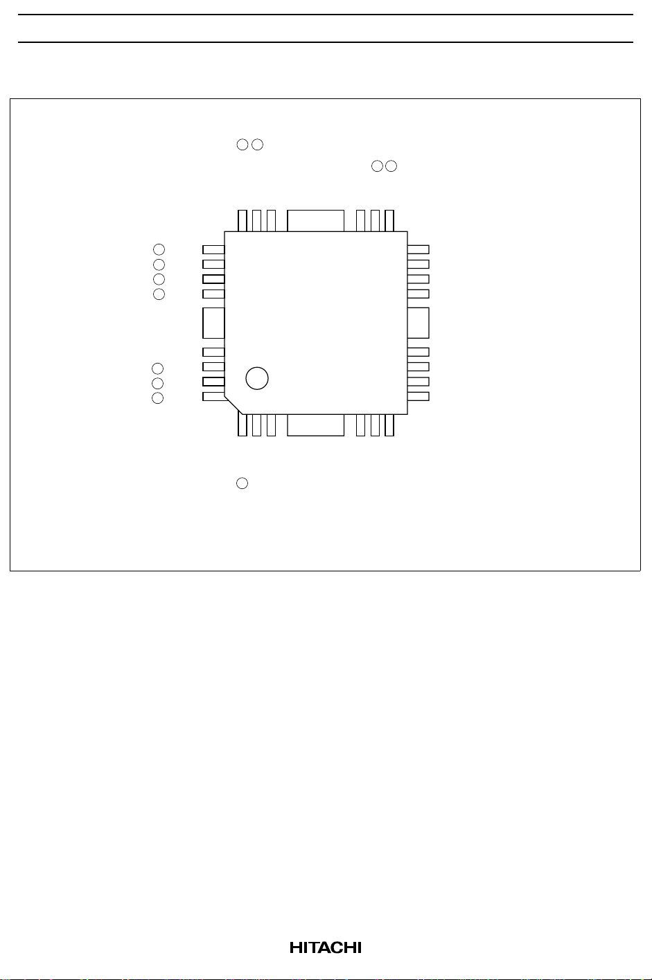
Pin Arrangement
CC
U phase – input
U phase + input
V
Hall bias
Bias – pin
Bias + pin
V phase + input
V phase – input
W phase + input
W phase – input
AGC
Index + input
Index – input
FG + input
18
19
20
21
22
23
24
TAB
25
26
27
28
123
RPM SEL
FG – input
TAB
TAB
Index adjust
(Top view)
16 15
17
14
13
12
11
TAB
10
456
CE
Index Vreg
Index output
Bias output
U phase output
V phase output
Current detection
W phase output
9
Phase compensation
8
Charge pump output
7
CLK input
2
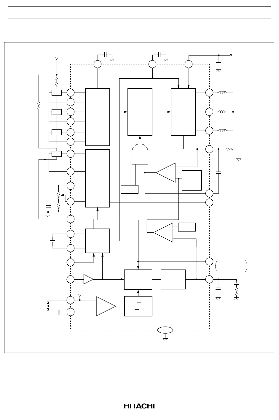
Block Diagram
HA13536F
R102
60 ppr
R101
Ct
C104
FG
V
CC
Hu
Hv
Hw
Hi
Rt1
CE
CLK
1 MHz
C103
Rt2
19
20
21
22
23
24
26
27
17
16
15
28
3
4
6
7
1
1.6 V
C102 C105
25 14 18
u (+)
u (-)
Hall
v (+)
v (-)
w (+)
w (-)
(+)
(-)
Index
circuit
Bias
FG Amp.
Amp
+
–
OTSD
Speed
discrim-
inator
Matrix
Control Amp.
–
+
–
+
Buffer Amp.
Charge
pump
Output
Amp
Current
limitter
Vref2
U
V
W
Vref1
C101
13
12
10
11
Rnf
C106
9
Index output
5
(Open collector)
RPM select
2
H: 360 rpm
L: 300 rpm
8
C1
V
CC
5 V
C2
R2
Note : Pin arrangement is preliminary specification.
TAB
3

HA13536F
O
Pin Function
Pin Number Pin Name Function Pin Voltage
1 FG (–) input FG Amp. (–) input terminal
2 RPMSEL Change terminal for motor rotation speed
“L” → 300 rpm, “H” → 360 rpm
3 Index adjustment Terminal to set up burst time of index circuit 0 V Min, 1.2 V Max
4 Index Vreg Output terminal for fixed voltage of index circuit 1.5 V Typ
5 Index output Index output terminal (Open collector) V
6 CE Chip enable terminal
“L”: enable, “H”: disable
7 CLK input CLK input terminal VTH = 1.4 V Typ
8 C-PUMP output Speed error Integration and Phase compensation of
speed control
9 Phase compensation To prevent the parastic oscillation of output, insert
the capacitor between pin 9 and pin 11.
10 W phase output W phase output
11 Current detection Output current detection and terminal which is con-
nected with phase compensation capacitor for car-
rent control.
12 V phase output V phase output
13 U phase output U phase output
14 Bias output Bias output terminal
15 Bias (+) pin Bias (+) pin terminal
16 Bias (–) pin Bias (–) pin terminal
17 Hall bias Hall bias terminal
CE = “L” → Bias,
CE = “H” → High impedance
18 V
CC
Power supply 4.25 V Min, 6.5 V
19 U phase (+) input U phase (+) input terminal 2.0 V Min,
20 U phase (–) input U phase (–) input terminal 2.0 V Min,
21 V phase (+) input V phase (+) input terminal 2.0 V Min,
22 V phase (–) input V phase (–) input terminal 2.0 V Min,
23 W phase (+) input W phase (+) input terminal 2.0 V Min,
24 W phase (–) input W phase (–) input terminal 2.0 V Min,
25 AGC Hall amp output wave form adjustment terminal
(Insert capacitor C102 between GND)
VTH = 1.4 V Typ
= 0.14 V Typ
L
(@I
= 2 mA)
O
VTH = 1.4 V Typ
2.2 V Typ
(@I = 10 mA)
Max
V
– 0.5 V Max
CC
V
– 0.5 V Max
CC
V
– 0.5 V Max
CC
V
– 0.5 V Max
CC
V
– 0.5 V Max
CC
V
– 0.5 V Max
CC
4

HA13536F
Pin Function (cont)
Pin Number Pin Name Function Pin Voltage
26 Index (+) input Index amp (+) input terminal 1.4 V Min,
– 0.5 V Max
V
CC
27 Index (–) input Index amp (–) input terminal 1.4 V Min,
V
– 0.5 V Max
CC
28 FG (+) input FG amp (+) input terminal DC bias 1.6 V Typ
External Parts
Part Number Recommended Value Purpose Notes
R2 — Integration constant 1
R101 — Hall bias
R102 — Index hall bias
Rnf — Current detection and limitation 2
Rt1 0 to 50 kΩ Index burst adjustment 3
Rt2 100 kΩ Index pulse width setting
C1, C2 — Integration constants 1
C101 ≥ 0.1 µF Power supply bypass 4
C102 0.1 µF AGC filter 5
C103 0.47 µF FG amp. coupling 5
C104 0.1 µF Bias
C105 ≥ 0.1 µF Bias 7
C106 0.1 µF Phase compensation 4
Ct 0.1 µF Index setting 3, 6
Notes: 1. Determine the integration constants from the following formulas:
2πf
ω
O
R2 =
C1 =
FG
≤
20
Jω
K
ω
O
N
O
Gctl Icp
T
1
R2
O
1
9.55
1
10
.
Rnf
(rad/s)
(Ω)
(F)
C2 = 10C1
(F)
5
 Loading...