HIT HA13156 Datasheet

HA13156
38 W × 4-Channel BTL Power IC
ADE-207-241 (Z)
1st. Edition
July 1997
Description
The HA13156 is four-channel BTL amplifier IC designed for car audio, featuring high output and low
distortion, and applicable to digital audio equipment. It provides 38 W output per channel, with a 13.7 V
power supply and at Max distortion.
Functions
• 4 ch BTL power amplifiers
• Built-in standby circuit
• Built-in muting circuit
• Built-in protection circuit (surge, T.S.D, and ASO)
• Built-in change booster ON/OFF circuit
Features
• High power for booster circuit
• Popping noise minimized
• Low output noise
• Built-in high reliability protection circuit

HA13156
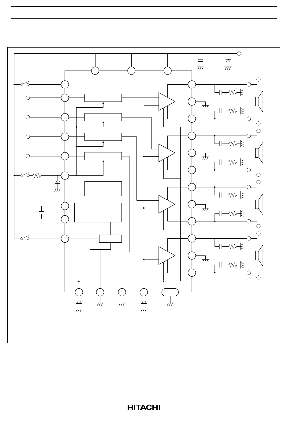
Block Diagram
SW1
IN2
IN3
SW2
C12
R9
4.7µ
7.5k
BST1
C14
0.47µ
BST2
SW3
BSTSW
2 STBY
1IN1
11
12
28IN4
10
+
MUTE
15
17
13
BSTOUT
C13
100µ
16
INVCC
Buffer & Mute-1
Buffer & Mute-2
Buffer & Mute-3
Buffer & Mute-4
Protector
(ASO, Surge, TSD)
Booster
CLKGEN
19
18
+
BSTGND
PVCC1
INGND
C11
0.47µ
C10
2.2µ
24
PVCC2
Amp1
Amp2
Amp3
Amp4
TAB
3
PGND1
4 SP1
5
7
PGND2
8 SP2
9
21
PGND3
22 SP3
23
25
PGND4
26 SP4
27
6
2014
+
C9
4400µ
C1
0.1µ
C2
0.1µ
C3
0.1µ
C4
0.1µ
C5
0.1µ
C6
0.1µ
C7
0.1µ
C8
0.1µ
R1
2.2
R2
2.2
R3
2.2
R4
2.2
R5
2.2
R6
2.2
R7
2.2
R8
2.2
OUT1
OUT1
OUT2
OUT2
OUT3
OUT3
OUT4
OUT4
Unit R: Ω
+
–
+
–
+
–
+
–
C: F
VCC
+
C1 to C8 should be polyester film capacitors with no secondary resonance (non-inductive),
*
to assure stable operation.
2

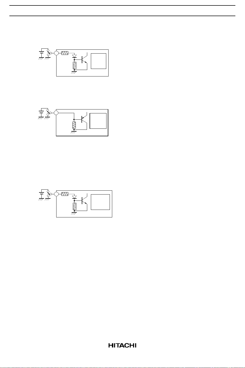
Note: 1. Standby
Power is turned on when a signal of 3.5 V or 0.05 mA is impressed at pin 2.
When pin 2 is open or connected to GND, standby is turned on (output off).
5 V
2. Muting
Muting is turned off (output off) when a signal of 3.5 V or 0.2 mA is impressed at pin 10.
When pin 10 is open or connected to GND, muting is turned on (output off).
5 V
3. DC-DC converter (Booster)
DC-DC converter (Booster) in IC is turned on when a signal of 3.5 V over or 0.04 mA over is
impressed at pin 13, and get large max output power.
When pin 13 is open or connected to GND, DC-DC converter (Booster) is turned off.
This IC is generated noise, because built-in DC-DC converter (Booster).
Consequently if you use radio tuner (AM), I recommend DC-DC converter (Booster) off.
5 V
HA13156
2
37.5 k
23.5 k
10
25 k
13
30 k
20 k
Q1 ON
↓
BIAS ON
Q2 ON
↓
MUTE ON
Q3 ON
↓
Booster ON
3

HA13156
Absolute Maximum Ratings
Item Symbol Rating Unit
Operating supply voltage V
Supply voltage when no signal*
Peak supply voltage*
Output current*
Power dissipation*
2
3
4
1
CC
VCC (DC) 26 V
VCC (PEAK) 50 V
IO (PEAK) 4 A
P
T
Junction temperature Tj 150 °C
Operating temperature Topr –30 to +85 °C
Storage temperature Tstg –55 to +125 °C
Note: 1. Tolerance within 30 seconds.
2. Tolerance in surge pulse waveform.
3. Value per 1 channel.
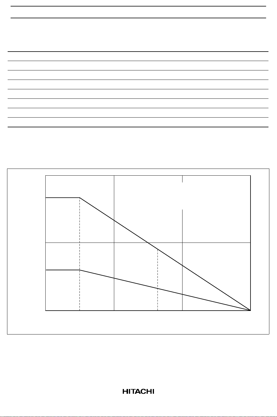
4. Value when attached on the infinite heat sink plate at Ta = 25 °C.
The derating carve is as shown in the graph below.
100
18 V
83 W
83 W
(W)
T
50
28 W
Power dissipation P
0
25
A: When heat sink is infinite (θj-a = 1.5°C/W)
B: When θf (thermal resistance of heat sink) = 3°C/W
(θj-a = 4.5°C/W)
A
B
50
85
100
Ambient temperature Ta (°C)
150
4

HA13156
Electrical Characteristics (VCC = 13.2 V, RL = 4 Ω, f = 1 kHz, Rg = 600 Ω, Ta = 25°C,
when there is no description in test conditions)
Item Symbol Min Typ Max Unit Test Conditions
Quiescent current1 I
Quiescent current2 I
Q1
Q2
Total harmonic distortion T.H.D. — 0.02 0.1 % Po = 3 W, boost on, off
Gain G
Gain difference between channels ∆G
Rated output power1 P
Rated output power2 P
Max output power1 P
Max output power2 P
V
V
O1
O2
OMAX1
OMAX2
Output noise voltage1 WBN1 — 0.15 0.3 mVrms Rg = 0 Ω, mute off,
Output noise voltage2 WBN2 — 0.08 0.2 mVrms Rg = 0 Ω, mute on,
Ripple rejection SVR 45 55 — dB f = 120 Hz
Output offset voltage1 ∆V
Output offset voltage2 ∆V
Standby current I
Standby control voltage (high) V
Standby control voltage (low) V
Muting control voltage (high) V
Muting control voltage (low) V
Boost control voltage (high) V
Boost control voltage (low) V
Q1
Q2
ST
STH
STL
MH
ML
BH
BL
Muting attenuation ATTM 70 90 — dB Vout = 6.7 Vrms
Channel cross talk C.T. 60 80 — dB Vout = 6.7 Vrms
Input impedance Zin 18 25 33 kΩ
Input voltage muted completly ATTin 7 — — Vp-p
Note: boost on; Boost control voltage (high),
mute on; Muting control voltage (low)
275 380 480 mA Vin = 0 V, boost on, RL = ∞
190 320 420 mA Vin = 0 V, boost off, RL = ∞
30.5 32 33.5 dB
–1.0 0 1.0 dB
20 23 — W VCC = 13.2 V, boost on,
RL = 4 Ω, THD = 10%
17 20 — W VCC = 13.2 V, boost off,
RL = 4 Ω, THD = 10%
35 38 — W VCC = 13.7 V, boost on,
RL = 4 Ω
31 34 — W VCC = 13.7 V, boost off,
RL = 4 Ω
BW = 20 to 20 kHz
BW = 20 to 20 kHz
–250 0 250 mV Vin = 0 V, mute off
–250 0 250 mV Vin = 0 V, change value
of mute on → off
—1 10µA boost off
3.5 — V
CC
V
0 — 1.5 V
3.5 — V
CC
V
0 — 1.5 V
3.5 — V
CC
V
0 — 1.5 V
5

HA13156
Characteristic Curves
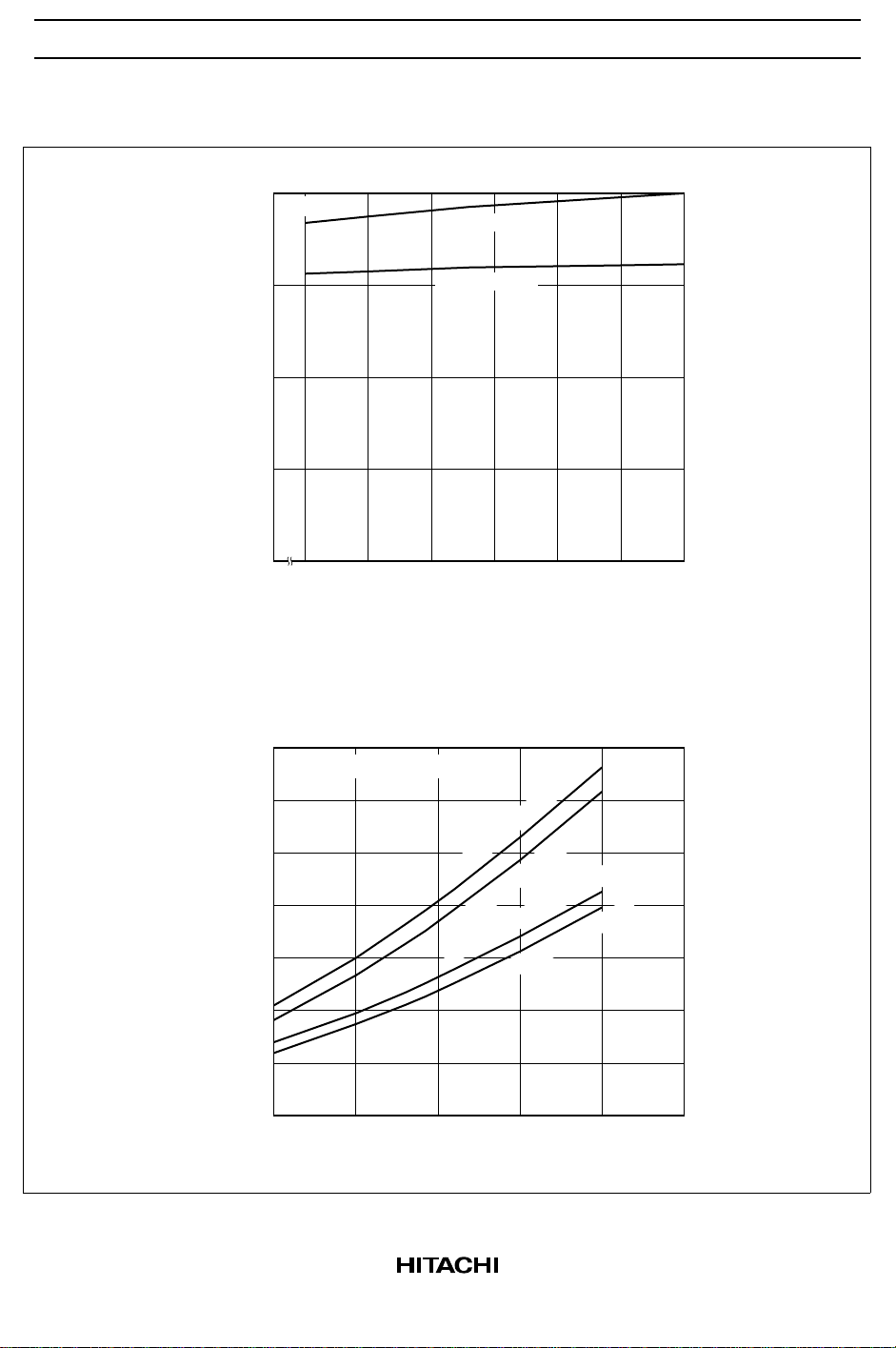
400
Quiescent current vs. Supply Voltage
= ∞
R
L
Booster ON
300
(mA)
Q
200
100
Quiescent current I
0
8 101214161820
0
70
RL = 4 Ω, f = 1 kHz
60
Booster OFF
Supply Voltage V
CC
(V)
Output Power vs. Supply Voltage
50
Pomax (Booster ON)
40
Pomax (Booster OFF)
30
20
Po (THD = 10 %, Booster ON)
Po (THD = 10 %, Booster OFF)
Output Power Po, Pomax (W)
10
0
10
12 14 16 18 20
Supply Voltage V
CC
(V)
6
 Loading...