HIT HA13150A Datasheet

HA13150A
21 W × 4-Channel BTL Power IC
ADE-207-107
1st. Edition
Description
HA13150A is a four-channel BTL amplifier IC designed for car audio, featuring high output and low
distortion, and applicable to digital audio equipment. It provides 21 W output per channel, with a 14.4
V power supply and at 10% distortion.
Functions
• Built-in standby circuit
• Built-in muting circuit
• Built-in protection circuits (surge, TSD, and ASO)
Features
• Requires few external parts
• Low distortion (total harmonic distortion = 0.01% at 3 W)
• Low noise (at Rg = 620 Ω, noise is 0.15 mV (muting off) or 0.1 mV (muting on))
• Popping noise minimized
• Highly reliable current-limiting ASO protector keeps speakers safe from all kinds of trouble.
Reliability is further enhanced by a fast-acting thermal shutdown protection circuit with on/off
hysteresis.

HA13150A
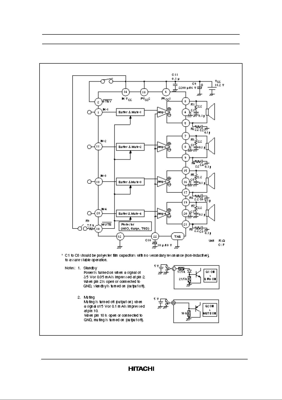
Block Diagram
Absolute Maximum Ratings (Ta = 25°C)
Item Symbol Rating Unit Remarks
2

HA13150A
Operating supply voltage V
CC
18 V
Supply voltage when no signal *1VCC (DC) 26 V
Peak supply voltage *
Output current *
Power dissipation *
2
3
4
VCC (PEAK) 50 V
IO (PEAK) 4 A
P
T
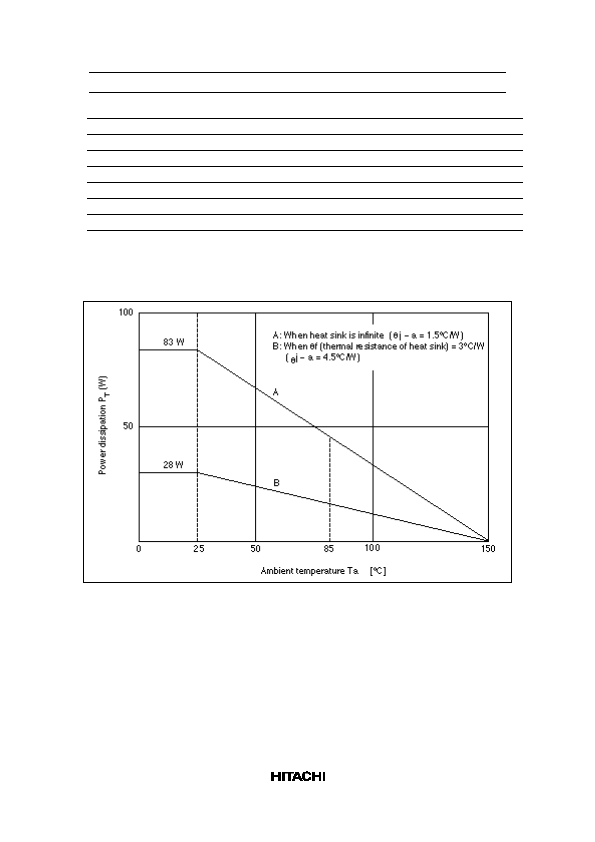
83 W
Junction temperature Tj 150 °C
Operating temperature Topr –30 to +85 °C
Storage temperature Tstg –55 to +125 °C
Notes: 1. Tolerance within 30 seconds
2. Tolerance in surge pulse waveform
3. Value per 1 channel
4. Value when attached on the infinite heat sink plate at Ta = 25°C.
The derating carve is as shown in the graph below.
3

HA13150A
Electrical Characteristics (VCC = 13.2 V, f = 1 kHz, RL = 4 Ω, Rg = 620 Ω, Ta =
25°C)
Item Symbol Min Typ Max Unit Test Conditions
Current when no signal Iq1 — 240 — mA Vin = 0
Output offset voltage ∆Vq –250 0 +250 mV
Gain Gv 30.5 32 33.5 dB
Gain difference between
channels
Rated output power Po — 18 — W VCC = 13.2 V
Max output power Pomax — 30 — VCC = 13.7 V
Total harmonic distortion T.H.D — 0.01 — % Po = 3 W
Output noise voltage WBN — 0.15 0.5 mVrms Rg = 0 Ω
Ripple rejection SVR — 55 — dB Rg = 600 Ω
Channel crosstalk C.T — 70 — dB Rg = 600 Ω
Input impedance Rin — 25 — kΩ
Standby current Iq2 — — 200 µA
Standby control voltage
(high)
Standby control voltage
(low)
Muting control voltage
(high)
Muting control voltage
(low)
Muting attenuation A
∆Gv –1.5 0 +1.5 dB
V
STH
V
STL
V
MH
V
ML
TTM
3.5 — V
CC
V
0 — 1.5 V
3.5 — V
CC
V
0 — 1.5 V
— 70 — dB Vout = 0 dBm
RL = 4 Ω, THD = 10%
RL = 4 Ω, THD = Max
BW = 20 to 20 kHz
f = 120 Hz
Vout = 0 dBm
4

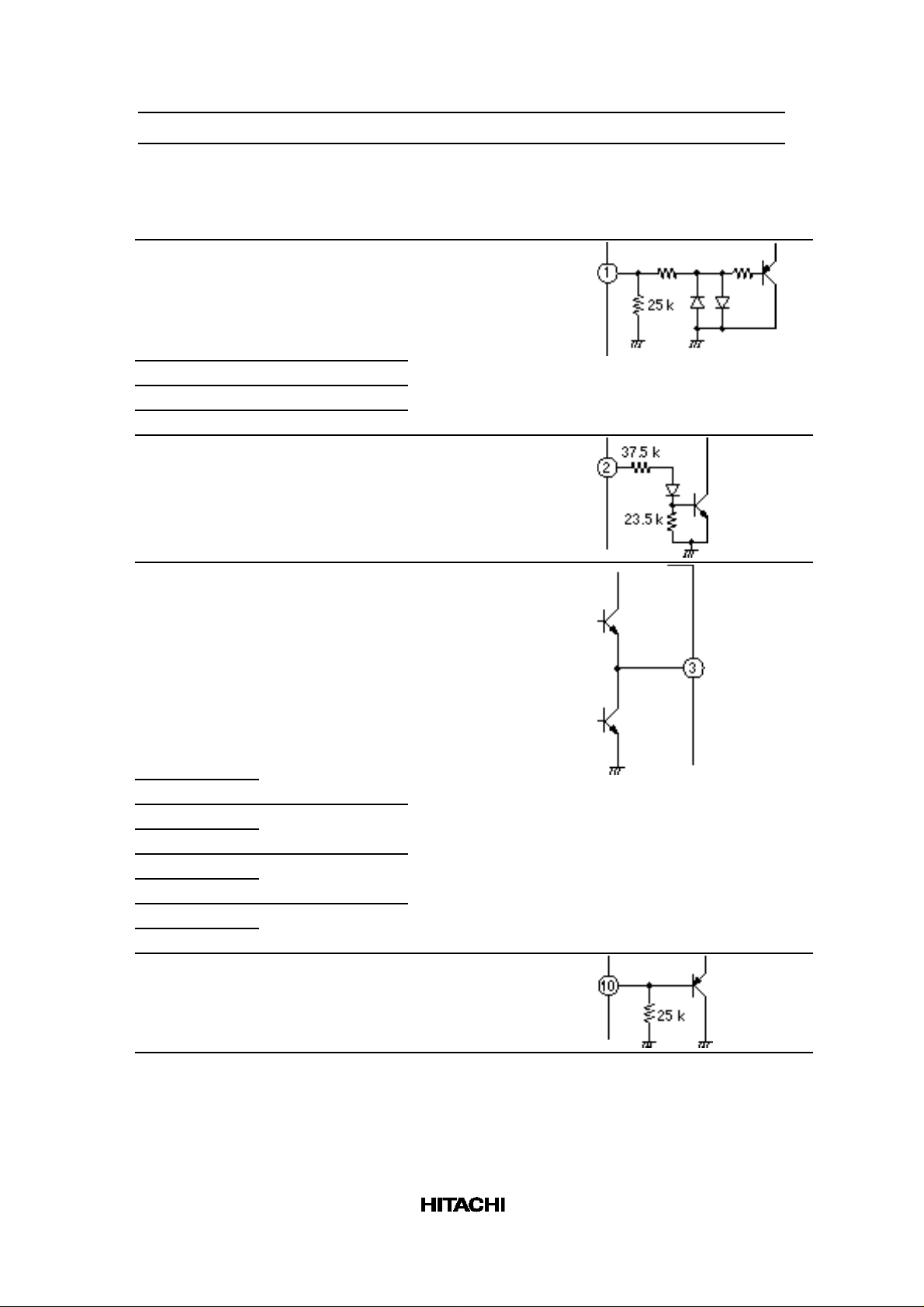
Pin Explanation
HA13150A
Pin
No. Symbol Functions
1 IN1 CH1 INPUT 25 kΩ (Typ) 0 V
11 IN2 CH2 INPUT
13 IN3 CH3 INPUT
23 IN4 CH4 INPUT
2 STBY Standby control 90 kΩ
3 OUT1 (+) CH1 OUTPUT — VCC/2
Input
Impedance
(at Trs. cutoff)
DC
Voltage Equivalence Circuit
—
5 OUT1 (–)
7 OUT2 (+) CH2 OUTPUT
9 OUT2 (–)
15 OUT3 (+) CH3 OUTPUT
17 OUT3 (–)
19 OUT4 (+) CH4 OUTPUT
21 OUT4 (–)
10 MUTE Muting control 25 kΩ (Typ) —
5
 Loading...