


HA12220F
CD-ROM Drive Head Amplifier IC
ADE-207-230 (Z)
Target Specification
1st. Edition
April 1997
Functions
• RF amplifier (Built-in equalizer changing cir cuit)
• Focus error amplifier (fc = 60kHz Typ)
• Tracking error amplifier (Built-in cut-off frequency changing circuit fc = 30kHz, 60kHz, 100kHz,
200kHz Typ)
• FOK detection circuit (Built-in Vth changing circuit)
• Mirror detection circuit
• Defect detection circuit
• APC amplifier
• RFAGC amplifier
Features
• Built-in variable resistors (+14 to –16% 2% steps) for adjusting tracking error EF balance
• Built-in variable resistors (–8 to +8dB 4dB steps) for rough adjusting tracking gain
• Built-in variable resistors (–8 to +8dB 4dB steps) for rough adjusting focus gain
• Built-in focus offset insertion cir cuit (–0.7 to +0.7V in 0.1V steps)
• RF amplifier frequency characteristics 30MHz (–3dB) in case of peaking off
• High-speed access support (The mirror circuit internal time constant can be switched between normal,
4× and 8× modes.)
• Support for CD-RW playback
• Few external components
• Available to set the stand-by mode
• FP-28TB package
HA12220F
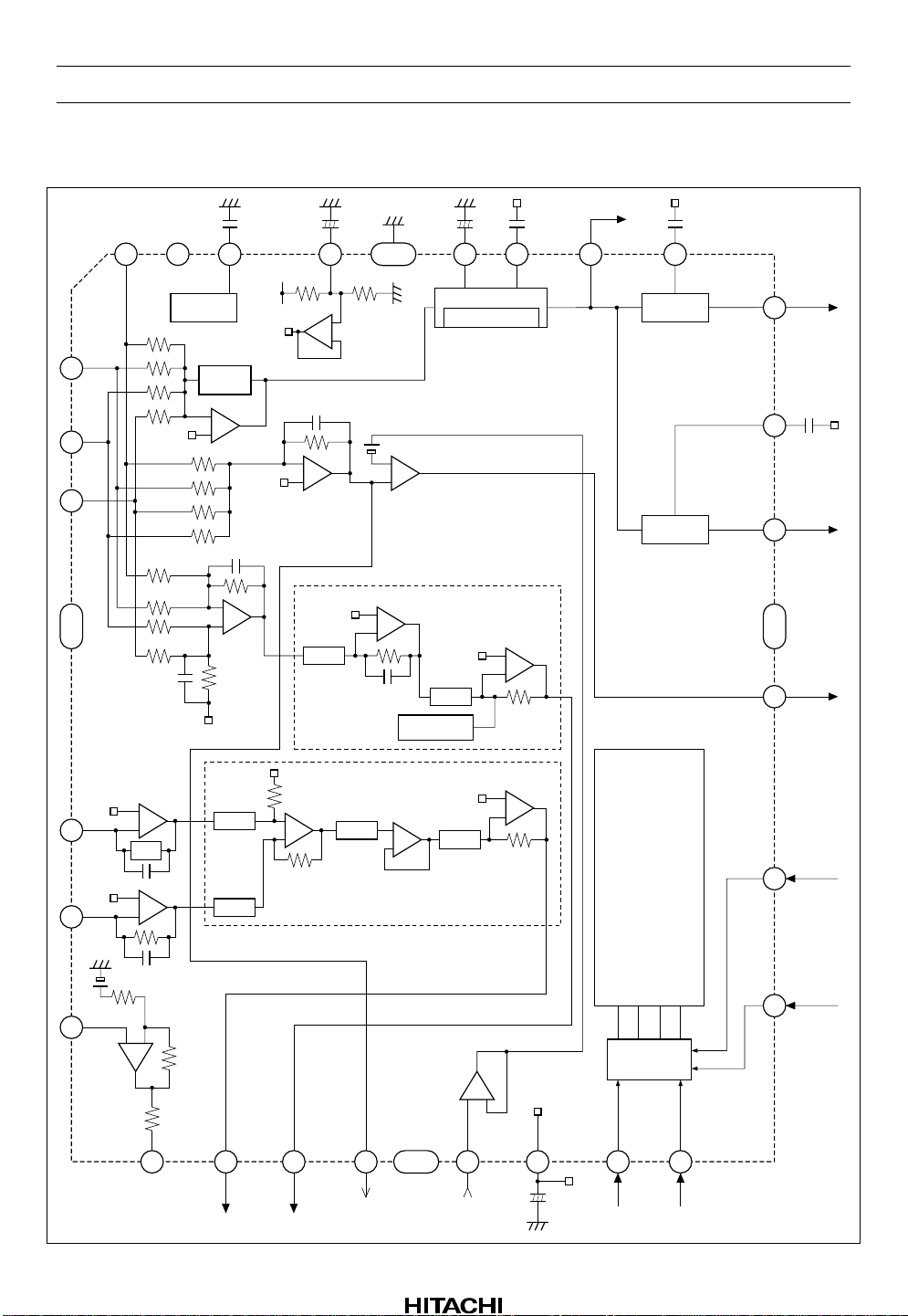
Block Diagram
RF2
1
RF3
2
RF4
3
GND
28
RF1
27
V
CC
BIAS
EQ
–
+
26
RFS
–
+
0.1µ
BYPS
FE
10µ
+
25
+
–
–
+
FSA
FVR2
GND 23
VCF RFC
VCB
FOK
+
–
FA2
+
–
Offset
1µ
+
24
AGC
Gain changing
Gain=12dB Typ
FA
+
–
FVR
0.1µ
AGCF
HD49250
22
AGCO
0.015µ
21
DFH
DEFECT
MIRR
DFT
MIRH
MIRR
FOK
20
HD49250
19
0.033µ
18
HD49250
GND
17
HD49250
TR1
APC
+
+
–
BAL
+
–
–
TR2
LD
7
TVR
TVR
TE
8
HD49250
HD49250
TR1
4
TR2
5
MD
6
Rev.1, Apr. 1997, page 2 of 20
FE
TA
11
+
CO
–
100µ
+
–
XLT
DATA
16
HD49250
15
HD49250
VC
IIL
Interface
12 13 1410
XRST
+
µ-COM
CLK
HD49250
TE
+
TLPF
–
9
CI
µ-COM
ADC
+
TVR2
–
Gain=8dB Typ
BUF
GND
µ-COM
DAC
HA12220F
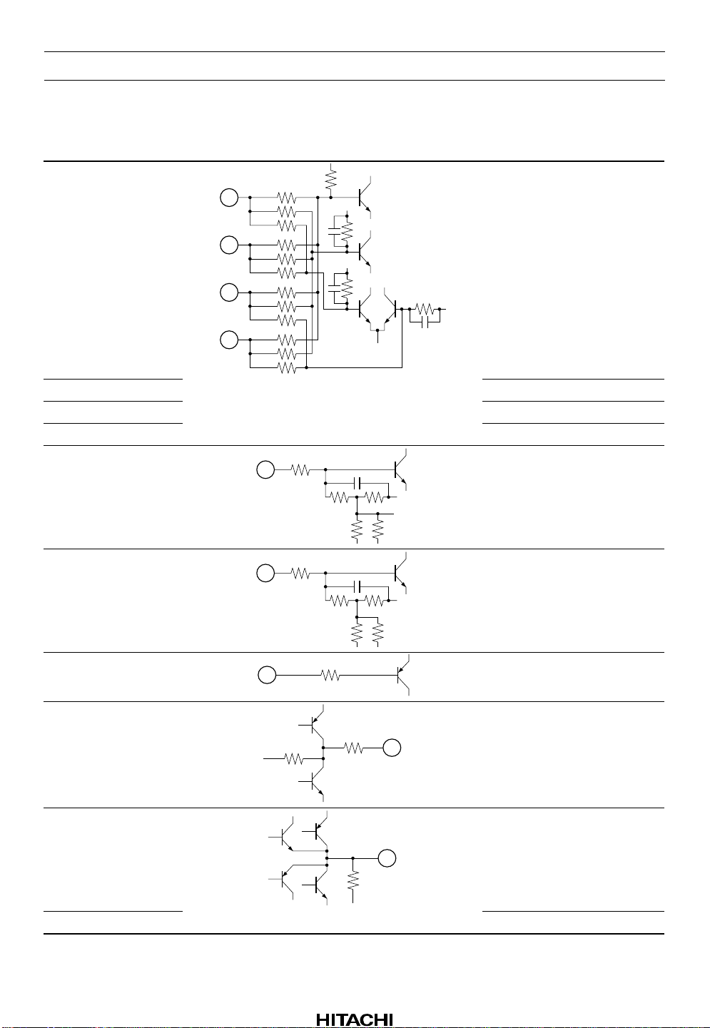
Pin Description and Equivalent Circuit
Pin No. Pin Name Equivalent Circuit Function
1RF2
28
12k
120k
160k
12k
1
120k
160k
12k
2
120k
160k
12k
3
120k
160k
5p
10p
4k
600k
160k
160k
10p
2 RF3 RF FE FSA amplifier input3
3 RF4 RF FE FSA amplifier input4
28 RF1 RF FE FSA amplifier input1
4TR1
4k
1.2p
RF FE FSA amplifier input2
TR1 amplifier input
5TR2
6MD
7LD
8TE
150k
4k
32k80k
40k 11.4k
1.2p
32k80k
40k 11.4k
4k
1k
40k
TR2 amplifier input
APC amplifier input
APC amplifier output
Tracking error signal output
9 FE Focus error signal output
Rev.1, Apr. 1997, page 3 of 20
HA12220F
Pin Description and Equivalent Circuit (cont)
Pin No. Pin Name Equivalent Circuit Function
10 CI
2.5k
FSA amplifier output monitor
11 CO
12 VC
13 XRST
10k
20k
4k
Setting FOK reference voltage
Reference voltage output
Reset input
14 CLK Serial data synchronous clock
input
15 DATA Serial data input
16 XLT Serial data latch input
V
20k
10k
CC
V
CC
FOK detection signal output
Mirror detection signal output
17 FOK
18 MIRR
19 MIRH
20 DFT
Rev.1, Apr. 1997, page 4 of 20
100k
20k
Mirror envelope hold signal
output
V
CC
Defect detection signal output
Pin Description and Equivalent Circuit (cont)
Pin No. Pin Name Equivalent Circuit Function
21 DFH
Defect envelope hold signal
output
HA12220F
22 AGCO
23 AGCF
24 RFC
25 VCF
26 BYPS
5k 5k
100k 4k
2k 4k
20k
AGC amplifier output
Capacitor connection for AGC
Capacitor connection for AGC
V
CC
40k
4k
40k
GND
V
CC
Capacitor connection for
reference voltage ripple filter
Capacitor connection for ripple
filter
27 V
CC
—V
CC
Rev.1, Apr. 1997, page 5 of 20
HA12220F
Operation
Control by Serial Data
The IC’s internal switches can be operated by sending control data from the HD49250.
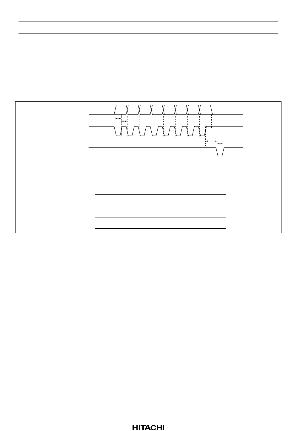
The signal timing is shown in figure 1, and the control commands are listed in table 1 and 2.
DATA
Pin 15
Pin 14
CLK
01234567
T1
T2
Pin 16
XLT
Item
Clock frequency
Clock pulse width
Delay time
Latch pulse width
Symbol
f
CLK
T1, T2
T3
T4
T3
Min Typ Max Unit
—
—
520
—
0.96
1
2
—
—
—
—
—
T4
kHz
µs
µs
µs
Figure 1 Timing Diagram for Serial Data Control
Signals from the HD49250 are input at pins 14 to 16. Pin13 is connected to the microcomputer.
A low input at the XRST pin resets the IC. Normally this pin should be kept high.
The serial data from the HD49250 switches the followin g settings.
1. Tracking error EF balance
2. Focus offset
3. Tracking gain, Focus gain
4. FOK Vth
5. Mirror circuit, defect circuit normal speed / 4× speed / 8× speed mode
6. Tracking error cut-off frequency
7. APC amplifier ON/OFF
8. RF equalizer
9. Stand-by mode (cleared by setting XRST on)
Rev.1, Apr. 1997, page 6 of 20

IIL
Interface
XLT
DATA
16
HD49250
15
HD49250
HA12220F
XRST
13 14
µ-COM
CLK
HD49250
Figure 2 Serial Data Control
Rev.1, Apr. 1997, page 7 of 20

HA12220F
Table 1 Serial Data Control Command 1
D7D6D5 D4 D3 D2 D1
Focus error gain
CD-RW
000
CD-RW
*1
DATA Note
D0
Focus error gain
D2
D3
0
0
1
0
1
0
0
1
1
1
D1
0
1
0
1
0
Gain (dB)
0
–4
–8
+7.9
+4.3
0
Focus error offset
Variable resistor BAL for
tracking error EF balance
001 0
010 0
D4
D4
1
0
D3
0
1
0
1
0
1
0
1
1
1
1
1
1
1
1
1
0
0
0
0
0
0
0
0
1
0
1
0
1
0
1
0
D2
0
0
1
1
0
0
1
1
0
0
1
1
0
0
1
1
D3
1
1
1
1
0
0
0
0
0
0
0
1
1
1
1
D1
0
1
0
1
0
1
0
1
0
1
0
1
0
1
0
1
D2
1
1
0
0
1
1
0
0
0
1
1
0
0
1
1
D1
1
0
1
0
1
0
1
0
1
0
1
0
1
0
1
BAL
336kΩ
344kΩ
352kΩ
360kΩ
368kΩ
376kΩ
384kΩ
392kΩ
400kΩ
408kΩ
416kΩ
424kΩ
432kΩ
440kΩ
448kΩ
456kΩ
Offset (V)
+0.7
+0.6
+0.5
+0.4
+0.3
+0.2
+0.1
±0
–0.1
–0.2
–0.3
–0.4
–0.5
–0.6
–0.7
Ratio
–16%
–14%
–12%
–10%
–8%
–6%
–4%
–2%
±0%
+2%
+4%
+6%
+8%
+10%
+12%
+14%
Note: 1. Both tracking error and focus error gains are increased by 12dB. The RFAGC block gain is
Rev.1, Apr. 1997, page 8 of 20
also increased by 12dB.

Table 2 Serial Data Control Command 2
D7D6D5 D4 D3 D2 D1
Tracking error gain Tracking error gain100 0—
HA12220F
DATA Note
D0
D2
D1
0
1
0
1
0
Gain (dB)
0
–4
–8
+7.9
+4.3
D3
0
0
0
1
1
0
1
1
0
1
Tracking error filter
Mirror
Defect
APC ON
FOK Vth
Stand-by
RFEQ
Note: 1.
Switches the mirror circuit and the defect circuit internal time constants at the same time.
Don’t use D3 = “1”, D2 = “0” mode.
The switch name surrouded by circle means that the switch turns on when the
2.
corresponding bit is “1”. This switch changes the value of the RF peaking capacitor.
In case of peaking off all switches must be set off.
101
110
111
Tracking error
filter
D1
D4
1
1
0
1
0
D4
1
0
0
1
1
0
0
FOK Vth
D3
1
1
0
0
30kHz
60kHz
100kHz
200kHz
–12dB
Prohibit
Mirror, Defect
D2
D3
0
0
1
0
1
1
Vth
–6dB
0dB
*1
Mode
Normal
4×
8×
Stand-byONAPC ON
0
0
Stand-by
mode is
cleared by
setting
XRST on.
0SC4 SC3 SC2 SC1 *2
Rev.1, Apr. 1997, page 9 of 20

HA12220F
RF Amplifiers
The output from PDIC is summed by RFS amplifier.
Figure 4 shows the equivalent circuit for the EQ block in figure 3. The peaking characteristics can be
changed with 4-bit data from the HD49250.
On resistance of SC1 to SC4 are 600Ω Typ.
28
RF1
RF2
1
RF3
2
RF4
3
12k
12k
12k
12k
EQ
–
+
to AGC
RFS
Figure 3 RFS Amplifier
4p 8p
SC3 SC2
1.58k
4k 4k
16p
SC1 SC4
0.3p
Figure 4 RFS Amplifier Equalizer Equivalent Circuit
The RFS amplifier output is input to the AGC am plifier internally in the IC.
Pin 24 is used to connect the capacitor that sets cut-o ff fr eque ncy of high-pass filter between the RFS
amplifier and the AGC amplifier. The cut-off frequency will typically b e 80Hz with the external constants
shown in figure 5.
The RF signal is rectified by an internal resistor and an external capacitor connected to pin 23.
The pins 28, 1, 2, and 3 expect an input level of about 0.1Vpp. The AGC amplifier output (pin 22) will
have an amplitude of 1.2Vpp Typ.
When CD-RW mode is set by 1-bit data from the HD49250, the AGC amplifier gain is increased by 12dB.
This allows the IC to output a 1.2Vpp Typ amplitude even during CD-RW playback.
from RFS
Rev.1, Apr. 1997, page 10 of 20
to HD49250
0.1µ
1µ
+
24 23
AGCFRFC
AGC
Gain changing
22
Figure 5 AGC Amplifier
AGCO
to DEFECT MIRR

HA12220F
FOK Detection Circuit
This detector is a comparator that generates the FOK signal. FOK is one of the signals that activate the
focus servo.
The FSA amplifier (fc = 53kHz Typ) summes the output from the PDIC. When this output signal becomes
lower than the reference voltage by Vth, pin 17 goes high. This Vth can be set by 2-bit data from the
HD49250.
Vth is set to 0.8V (0dB) after a reset.
Using µ-com ADC & DAC the voltage of pin 11 had better be set the same voltage as the voltage of pin 10
before focus searching in order to reduce the effect of DC offset voltage at FSA amplifier output.
BUF
28
5p
600k
RF1
RF2
1
RF3
2
RF4
3
120k
120k
120k
120k
+
–
FSA
FOK
+
–
–
+
11 µ-COM DAC
CO
FOK
17
CI
10
µ-COM ADC
Figure 6 FOK Detection
APC
This circuit is for the Psub laser diode. This circuit is turned on or off by 1-bit data from the HD49250.
MD
6
APC
+
–
1k
LD
7
Figure 7 APC
Rev.1, Apr. 1997, page 11 of 20

HA12220F
;
;
;
;
;
;
;
Focus Error Amplifiers
The FE amplifier adds and subtracts the output from the PDIC.
FVR2 is a variable resistor used to increase the gain by 12dB in CD-RW mode. This variable resistor is set
by 1-bit data from the HD49250.
FVR is a variable resistor that changes the focus error gain over the range –8 to +8dB in ±4dB steps. This
variable resistor is set by 3-bit data from the HD49250.
An offset of between –0.7 and 0.7V (in 0.1V steps) is inserted into the focus error signal. This is set by 4bit data from the HD49250. The FE output cut-off frequency (fc) is 60kHz Typ.
10p
160k
28
RF1
160k
RF2
1
RF3
2
160k
RF4
3
160k
10p
160k
–
+
FE
+
FA2
–
Gain=12dB Typ
FVR2
160k
160k
10p
FVR
Offset
Figure 8 Focus Error Amplifiers
FA
+
–
9
FE
Defect Detection Circuit
When a scratched disc is played, the EFM RF signal has the shape shown in figure 10 (a). The defect
detection circuit detects the drop-out area of this signal.
0.015µ
21
DFH
DFT
MIRH
MIRR
20
HD49250
19
0.033µ
18
HD49250
from AGC
DEFECT
MIRR
Figure 9 Mirror Detection, Defect Detection
;;;;;;;;;;;;;;;;;;;
;;;;;;;;;;;;;;;;;;;
(a) Pin 22
(b) Pin 20
;;;;;;;;;;;;;;;;;;;
;;;;;;;;;;;;;;;;;;;
;;;;;;;;;;;;;;;;;;;
;;;;;;;;;;;;;;;;;;;
;;;;;;;;;;;;;;;;;;;
Rev.1, Apr. 1997, page 12 of 20
Figure 10 Defect Detection Waveform

HA12220F
Mirror Detection Circuit (MIRR)
As the pick-up travels across tracks, the EFM RF signal varies as in figure 11 (a). The mirror detection
circuit detects the mirror region from this signal.
The external capacitor on pin 19 integrates the track-crossing frequency component.
The internal time constant of the mirror detection circuit can be set for normal, 4×, or 8× speed by 2-bit
data from the HD49250, to raise the trackable range of track-crossing frequencies. The defect circuit
internal time constant is also switched at the same tim e.
(a) Pin 22
(b) Pin 18
Figure 11 Mirror Detection Waveform
Tracking Error Amplifiers
The sub-beam output of PDIC is passed through a resistor and input at pins 4 and 5. External resistances of
pins 4 and 5 should be set according to the pick-up so that the traverse signal at pin 8 is about 2Vpp Typ.
After a reset, the initial value of the feedback resistance BAL of TR1 am plifier is 400kΩ, the same as the
feedback resistance of TR2 amplifier.
BAL has a variable resistance value that is changed by 4-bit data from the HD49250. The variability range
here is from –16 to +14% in 2% steps. This resistance can be varied to adjust the EF balance of the
tracking error.
TE amplifier generates the tracking error signal.
TVR is a resistor that changes the tracking gain from –8 to +8dB in 4dB steps. This is set by 3-bit data
from the HD49250. TVR2 is a variable resistor used to increase the gain by 12dB in CD-RW mode. This
variable resistor is set by 1-bit data from the HD49250.
TLPF switches the tracking error cut-off frequency. The TE output cut-off frequency is set to either 30, 60,
100, or 200kHz (Typ) by 2-bit data from the HD49250.
4
5
TR1
TR2
TR1
+
–
BAL
1.2p
+
–
400k
1.2p
TR2
TVR
TVR
TE
+
–
TLPF
Figure 12 Tracking Error Amplifiers
+
TVR2
–
Gain=8dB Typ
TA
+
–
8
TE
Rev.1, Apr. 1997, page 13 of 20

HA12220F
Bias, Reference Voltage
Pin 26 is for a bypass capacitor to eliminate noise f r om the IC’s internal bias circuits.
Connect a capacitor to pin 25 to remove the ripple component from the reference voltage.
The IC’s internal reference voltage is connected internally.
27
V
CC
BIAS
0.1µ
26
BYPS
12
25
+
–
10µ
+
VCF
VCB
GND
40k40k
Figure 13 Bias, Reference Voltage
Rev.1, Apr. 1997, page 14 of 20

HA12220F
Absolute Maximum Rating (Ta=25°C)
Item Symbol Rating Unit
Power supply voltage V
Power dissipation P
CC
T
Operating temperature Topr –20 to +75 °C
Storage temperature Tstg –55 to +125 °C
Note: Recommended operating power supply voltage : 5V ± 0.5V
6V
400 mW
Rev.1, Apr. 1997, page 15 of 20

HA12220F
Electrical Characteristics (Ta = 25°C, VCC = 5V)
Item Symbol Min Typ Max Unit Test Conditions
Quiescent current 1 I
Quiescent current 2 I
Reference voltage V
Focus error
Offset voltage *
1
CC1
CC2
C
V
FE
amp.
Tracking
Max output voltage H 1 V
Max output voltage L 1 V
Max output voltage H 2 V
Max output voltage L 2 V
Voltage gain 1 G
Voltage gain 2 G
Offset voltage *
1
FEH1
FEL1
FEH2
FEL2
VFE1
VFE2
V
TE
error amp.
Max output voltage H 1 V
Max output voltage L 1 V
Max output voltage H 2 V
Max output voltage L 2 V
Voltage gain 1 G
Voltage gain 2 G
FOK FOK Vth V
“H” output voltage V
“L” output voltage V
TEH1
TEL1
TEH2
TEL2
VTE1
VTE2
FOK
FKH
FKL
Note: 1. All offset voltages are values referring to VC (pin 12) at reset.
2. V11 = setting the same voltage as the voltage of pin 10 at no signal.
— 20 32 mA No si gnal 27
— 0.6 1.0 mA St and-by m ode
2.3 2.5 2.7 V I12 ≤ ±4mA 12
–
0 100 mV 9
100
4.2 4.5 — V S2, S3, S51, S9a
V51 = 4V
— 0.5 0.8 V S1, S28, S51, S9a
V51 = 4V
3.8 4.1 — V S2, S3, S51, S9b
V51 = 4V
— 0.9 1.2 V S1, S28, S51, S9b
V51 = 4V
16.0 18.0 20.0 dB S2, S3, S50
V9/VIN50
16.0 18.0 20.0 dB S1, S28, S50
V9/VIN50
–65 0 65 mV 8
4.2 4.5 — V S4, S51, S8a
V51 = 4V
— 0.5 0.8 V S5, S51, S8a
V51 = 4V
3.8 4.1 — V S4, S51, S8b
V51 = 4V
— 0.9 1.2 V S5, S51, S8b
V51 = 4V
5.0 8.0 11.0 dB S4, S50 V8/VIN50
5.0 8.0 11.0 dB S5, S50 V8/VIN50
110 160 210 mV S28, S51
when V17 ≥ 4V
Min (V51 – V12) *
4.7——V
——0.4V
Application
Terminal
17
2
Rev.1, Apr. 1997, page 16 of 20

HA12220F
Electrical Characteristics (Ta = 25°C, VCC = 5V) (cont)
Application
Item Symbol Min Typ Max Unit Test Conditions
Defect Max operation
frequency
Min operation
F
DH
2 — — kHz S28, S1, S2, S3,
S50, S23
F
DL
——1 kHz
frequency
“H” output voltage V
“L” output voltage V
Mirror Max operation
frequency
“H” output voltage V
“L” output voltage V
CLK DATA
“H” input voltage V
DFH
DFL
F
MIR
MIH
MIL
PH
4.7 — — V
——0.4V
200 — — kHz S28, S1, S2, S3,
S50, S23 8× mode
4.7 — — V
——0.4V
4.0 — — V 13, 14, 15,
XLT XRST
“L” input voltage V
APC APC voltage V
RFAGC Output voltage 1 V
PL
APC
AGC1
——1.0V
0.09 0.16 0.23 V 6
0.8 1. 2 1.6 Vp-p S28, S50, f = 200kHz
0.4Vpp ± 6dB input
Output voltage 2 V
AGC2
0.8 1. 2 1.6 Vp-p S1, S50, f = 200kHz
0.4Vpp ± 6dB input
Output voltage 3 V
AGC3
0.8 1. 2 1.6 Vp-p S2, S50, f = 200kHz
0.4Vpp ± 6dB input
Output voltage 4 V
AGC4
0.8 1. 2 1.6 Vp-p S3, S50, f = 200kHz
0.4Vpp ± 6dB input
Frequency
characteristics 1
Frequency
characteristics 2
Frequency
characteristics 3
Frequency
characteristics 4
F
AGC1
F
AGC2
F
AGC3
F
AGC4
— 30 — MHz S28, S50, S23
0.4Vpp input *
— 30 — MHz S1, S50, S23
0.4Vpp input *
— 30 — MHz S2, S50, S23
0.4Vpp input *
— 30 — MHz S3, S50, S23
0.4Vpp input *
3
3
3
3
Note: 3. Setting V23 at the value of the pin 23 voltage when S28 is on, VIN50 = 0.4Vpp, and a 200kHz
input. The frequency down –3dB from the output level for f = 200kHz.
Terminal
20
18
16
22
Rev.1, Apr. 1997, page 17 of 20

HA12220F
Test Circuit
S28
S1
S2
S3
S51
V23
0.1µ
10k
S22
2122
MIRR
0.015µ
20
19
18
10k
S20
0.033µ
10k
S18
S23
+
–
25
+
–
FSA
1µ
+
VCB
+
1µ
GND 23
Gain changing
FOK
+
–
24
AGC
CC
28
27 26
1
2
3
0.1µV
BIAS DEFECT
EQ
–
+
RFS
V51
S50
VIN50
S4
S5
390k
390k
560
2SB
561C
2k
0.1µ
4
5
6
GND
APC
+
+
–
BAL
+
–
–
TR1
TR2
7
–
+
FE
FVR2
S9a
+
–
S9b
TE
TLPF
2k20k
TVR
TVR
8 9 10 11
S8bS8a
2k20k
+
–
FA2
+
–
GND
FVR
Offset
TVR2
BUF
+
–
V11
FA
+
–
TA
+
–
IIL
12
+
13 14
10µ
Serial data generator
GND
17
16
15
10k
S17
Rev.1, Apr. 1997, page 18 of 20
Note: The symbol “●” of transfer switch shows OFF state.

Package Dimensions
9.0 ± 0.2
0.32 ± 0.08
0.30 ± 0.06
9.0 ± 0.2
7.0
20 15
0.65
21
28
1
0.575 0.575
14
7
6
M
0.13
1.40
1.7 Max
0.17 ± 0.05
0.15 ± 0.04
HA12220F
Unit: mm
1.0
0˚– 8˚
2.25 ± 0.1
0.10
+ 0.09
– 0.05
0.13
0.95 ± 0.10
0.50 ± 0.10
Hitachi Code
JEDEC Code
EIAJ Code
Weight
FP-28TB
—
—
0.19 g
Rev.1, Apr. 1997, page 19 of 20

HA12220F
Disclaimer
1. Hitachi neither warrants nor grants licenses of any rights of Hitachi’s or any third party’s patent,
copyright, trademark, or other intellectual property rights for information contained in this document.
Hitachi bears no responsibility for problems that may arise with third party’s rights, in cluding
intellectual property rights, in connection with u se of the information contained in this document.
2. Products and product specifications may be subject to change without notice. Confirm that you have
received the latest product standards or specifications before final design, purchase or use.
3. Hitachi makes every attempt to ensure that its products are of high quality and reliability. However,
contact Hitachi’s sales office before using the product in an application that demands especially high
quality and reliability or where its failure or malfunction may directly threaten human life or cause risk
of bodily injury, such as aerospace, aeronautics, nuclear power, combustion control, transportation,
traffic, safety equipment or medical equipment for life support.
4. Design your application so that the product is used within the ranges guaranteed by Hitachi particularly
for maximum rating, operating supply voltage range, heat radiation characteristics, installation
conditions and other characteristics. Hitachi bears no responsibility for failure or damage when used
beyond the guaranteed ranges. Even within the guaranteed ranges, consider normally foreseeable
failure rates or failure modes in semiconductor devices and employ systemic measures such as failsafes, so that the equipment incorporating Hitachi product does not cause bodily injury, fire or other
consequential damage due to operation of the Hitachi product.
5. This product is not designed to be radiation resistant.
6. No one is permitted to reproduce or duplicate, in any form, the whole or part of this document without
written approval from Hitachi.
7. Contact Hitachi’s sales office for any questions regarding this document or Hitachi semiconductor
products.
Sales Offices
Hitachi, Ltd.
Semiconductor & Integrated Circuits.
Nippon Bldg., 2-6-2, Ohte-machi, Chiyoda-ku, Tokyo 100-0004, Japan
Tel: Tokyo (03) 3270-2111 Fax: (03) 3270-5109
URL NorthAmerica : http://semiconductor.hitachi.com/
For further information write to:
Hitachi Semiconductor
(America) Inc.
179 East Tasman Drive,
San Jose,CA 95134
Tel: <1> (408) 433-1990
Fax: <1>(408) 433-0223
Europe : http://www.hitachi-eu.com/hel/ecg
Asia : http://sicapac.hitachi-asia.com
Japan : http://www.hitachi.co.jp/Sicd/indx.htm
Hitachi Europe GmbH
Electronic Components Group
Dornacher Straße 3
D-85622 Feldkirchen, Munich
Germany
Tel: <49> (89) 9 9180-0
Fax: <49> (89) 9 29 30 00
Hitachi Europe Ltd.
Electronic Components Group.
Whitebrook Park
Lower Cookham Road
Maidenhead
Berkshire SL6 8YA, United Kingdom
Tel: <44> (1628) 585000
Fax: <44> (1628) 585160
Hitachi Asia Ltd.
Hitachi Tower
16 Collyer Quay #20-00,
Singapore 049318
Tel : <65>-538-6533/538-8577
Fax : <65>-538-6933/538-3877
URL : http://www.hitachi.com.sg
Hitachi Asia Ltd.
(Taipei Branch Office)
4/F, No. 167, Tun Hwa North Road,
Hung-Kuo Building,
Taipei (105), Taiwan
Tel : <886>-(2)-2718-3666
Fax : <886>-(2)-2718-8180
Telex : 23222 HAS-TP
URL : http://www.hitachi.com.tw
Hitachi Asia (Hong Kong) Ltd.
Group III (Electronic Components)
7/F., North Tower,
World Finance Centre,
Harbour City, Canton Road
Tsim Sha Tsui, Kowloon,
Hong Kong
Tel : <852>-(2)-735-9218
Fax : <852>-(2)-730-0281
URL : http://www.hitachi.com.hk
Copyright Hitachi, Ltd., 2000. All rights reserved. Printed in Japan.
Colophon 2.0
Rev.1, Apr. 1997, page 20 of 20
 Loading...