HIT HA12211NT Datasheet

HA12211NT
Audio Signal Processor for Cassette Deck (Deck 1 Chip)
ADE-207-223A (Z)
2nd. Edition
June 1997
Description
HA12211NT is silicon monolithic bipolar IC providing REC equalizer system, PB equalizer system and
each electronic control switch in one chip.
Functions
• PB equalizer × 2 channel
• REC equalizer × 2 channel
• Each electronical control switch to change equalizer characteristics
• REC mute
• REC head return switch
Features
• REC equalizer is very small numb er of external parts.(4 types of frequency characteristics built-in )
• PB equalizer built-in. (A/B input changing system, 4 types of frequency characteristics)
• Independent PB sensitivity for A d eck, B d eck.
• Normal-speed/high-speed, normal tape/chr ome tape switching built-in.
• Controllable from direct micro-computer output.
• Available to reduce substrate-area because of high integration and small external parts.
HA12211NT
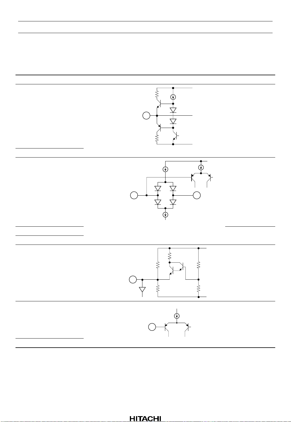
Pin Description, Equivalent Circuit (VCC = 10.5V, Vref = 5.25V, Ta = 25°C, No signal,
The value in the table show typical value.)
Pin No. Pin Name Note Equivalent Circuit Pin Description
1V
CC
V = V
CC
2 RECOUT (L) V = Vref
3RECOUT (R)
4 REC-RETURN V = Vref
V’ = Vref
V
CC
V
GND
V
I
CC
VCC Pin
REC-EQ output
REC Return
V4
5 pin, 6 pin
I
GND
V’
5 PB-IN B (L) PB B Deck input
6 PB-IN B (R)
7VREF V = Vref
V’ = V
/ 2
CC
8 PB-IN A(L) V = Vref
10k
V
10k
V
CC
V
CC
V’
GND
Reference
PB A Deck input
V
9 PB-IN A(R)
Rev.2, Jun. 1997, page 2 of 34
HA12211NT
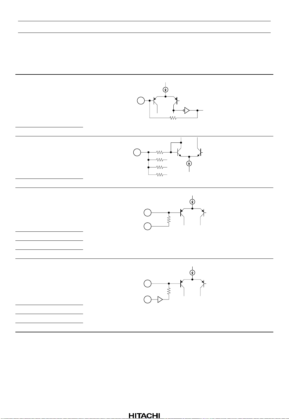
Pin Description, Equivalent Circuit (VCC = 10.5V, Vref = 5.25V, Ta = 25°C, No signal,
The value in the table show typical value.) (cont)
Pin No. Pin Name Note Equivalent Circuit Pin Description
10 PB-NF (L) V = Vref
11 PB-NF (R)
12 PB-EQ (L) V = Vref
13 PB-EQ (R)
14 PB-Cal A(L) V = Vref
V
CC
V
139k
V
GND
V
CC
PB EQ Feed back
NAB Output
Feed back input
for gain
adjustment
15 PB-Cal A(R)
16 PB-Cal B(R)
17 PB-Cal B(L)
26 AUX (R) V = Vref
27 AUX (L)
28 TAPE (R)
29 TAPE (L)
10k
7Vref V
100k
7Vref V
V
CC
REC-EQ input
Rev.2, Jun. 1997, page 3 of 34
HA12211NT
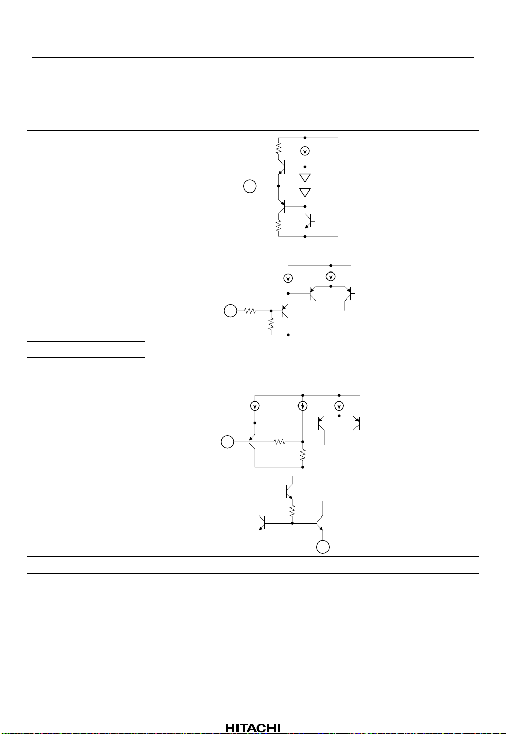
Pin Description, Equivalent Circuit (VCC = 10.5V, Vref = 5.25V, Ta = 25°C, No signal,
The value in the table show typical value.) (cont)
Pin No. Pin Name Note Equivalent Circuit Pin Description
18 PBOUT (R) V = Vref
19 PBOUT (L)
20 A/B I = 20µA
21 HSP
22 Acr
23 Bcr
24 REC-SEL I = 20µA
V = 2.5V
V
CC
V
GND
V
CC
I
22k
100k
GND
V
I
CC
PB output
Mode control input
Mode control input
100k
25 IREF V = 1.2V
V
50k
GND
Equalizer
reference current
input
V
30 GND GND Pin
Rev.2, Jun. 1997, page 4 of 34
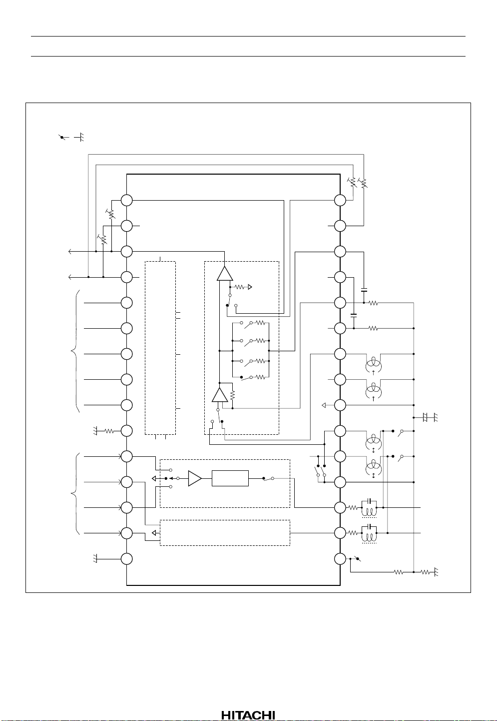
Block Diagram
CC
GND
V
HA12211NT
to Dolby
REC IN from logic
)
: 100kB
R
(L)
(R)
(L)
R
(L)
B
A/B
HSP
ACr
BCr
IREF
AUX
AUX
TAPE(
TAPE
)
R
(
B
)
L
(
B
(R)
PB-OUT
PB-OUT
19 18 17 16
21 20
22
REC-SEL
30 29 28 27 26 25 24 23
GND
PB-CAL
PB-CAL
L-ch
12dB
R-ch
B
: 100kB
B
PB-CAL
PB-CAL
–
+
10k
A
B
12 13 14 15
PB-EQ PB-EQ
PB-NF
10 11
9
5k 2.7k 2.26k 1.12k
–
+
139k
PB-IN PB-IN PB-NF
A
REC-EQ
PB-IN PB-IN
REC-RETURN
R
)
R
(
A
)
L
(
A
)
R
)(
L
(
0.022µ
)
R
(
0.022µ
)
L
470 470
)(
R
(
A
)
L
(
A
VREF
)
R
(
B
)
L
(
B
C : F
Unit R : Ω
470µ
+
R-ch
REC-OUT
(R)
470
Bias
470
L-ch
REC-OUT
(L)
5.6k 5.6k
CC
12345678
V
Rev.2, Jun. 1997, page 5 of 34

HA12211NT
Parallel Data Format
Pin No. Pin Name L M H
22 A CrO2 *
23 B CrO2 *
1, *3
1, *2, *3
21 HSP Normal speed *
20 A/B Ain active *
1, *3
Return SW ON *
REC OUT active *3—REC OUT Hiz
24 REC IN SEL TAPE MUTE *
Note: 1. PB-EQ LOGIC
HSP
LH
A/B
A CrO2 B CrO2 L H L H
L L 120µ 120µ 60µ 60µ
L H 120µ 70µ 60µ 35µ
HL70µ 120µ 35µ 60µ
HH70µ 70µ 35µ 35µ
—*
—*
3
—Hi speed
— Bin active *
3
— Return SW OFF
3
1
1, *2
1
AUX
2. REC-EQ LOGIC
HSP
B CrO2 L H
L Normal speed
TAPE I
H Normal speed
II
TAPE
3. Unforced pin state
High speed
TAPE I
High speed
II
TAPE
Rev.2, Jun. 1997, page 6 of 34
HA12211NT
Functional Description
Power Supply Range
This IC is designed to operate on single supply, shown by table 1.
Table 1 Spply Voltage
Item Power Supply Range
Single Supply 9.5V to 15.0V
Reference Voltage
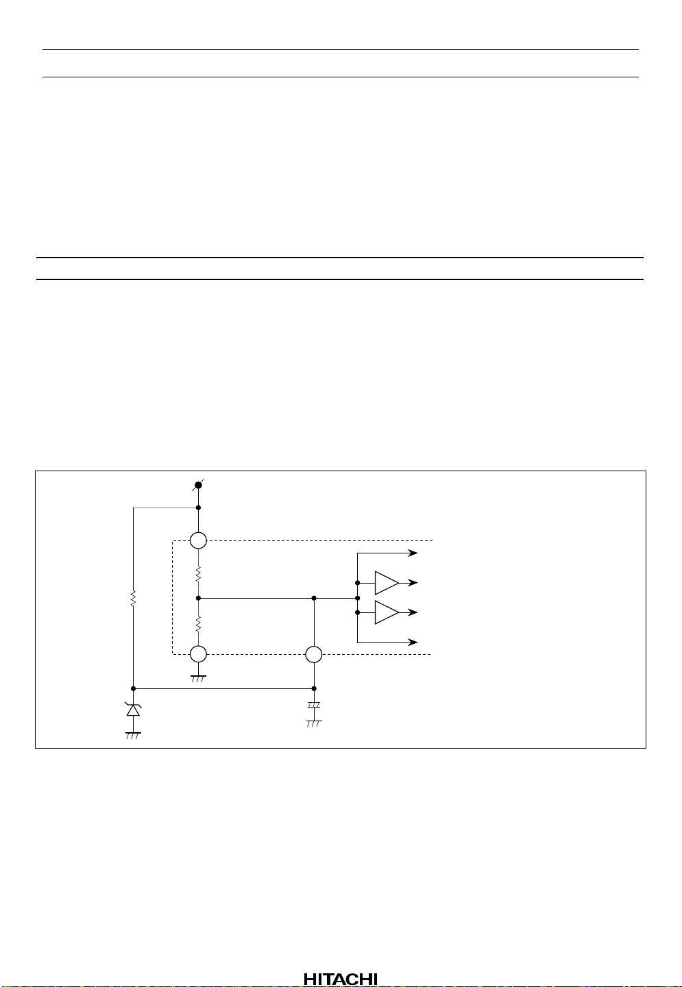
So little is the current drivability of AC refer ence (Vr ef) that the Vref voltage may be altered by A/B
switching of PB-EQ.
Provided it causes you anxiety, please use the constant 1/2 V
In addition, this IC has a capacitor charger for Vref pin.
V
CC
1
470Ω
30
GND
7
Vref
+
470µF
Figure 1 Reference Voltage Circuit
voltage circuit, for example, figure 1.
CC
Lch PB-EQ reference voltage
Lch REC-EQ reference voltage
Rch REC-EQ reference voltage
Rch PB-EQ reference voltage
Rev.2, Jun. 1997, page 7 of 34
HA12211NT
Operating Mode Control
This IC provides fully electronic switching circuits. And each operating mode control is controlled by
parallel data (DC voltage).
Table 2 Threshold Voltage (Vth)
Pin No. Lo Mid Hi Unit Test Condition
20, 21, 22, 23 0.0 to 2.5 — 4.0 to V
CC
V
Input Pin Measure
V
24 0.0 to 1.0 2.0 to 3.0 4.0 to V
CC
V
Note: 1. 20 to 23 pins are pulled down Lo level, and 24 pin is pulled to Mid level by the inside resistor
100kΩ.
2. Over shoot level and under shoot level of input signal must be the standardi ze d.
(High: V
, Low: –0.2V)
CC
Block Diagram
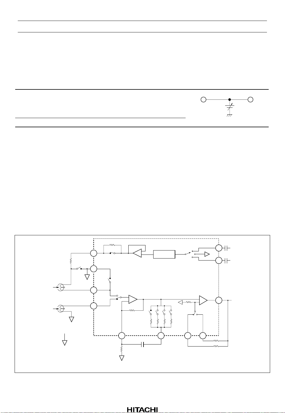
This IC can be constructed for simple system which has little external parts by used the head serving both
as Recording and Play back because of REC return SW built-in.
With output Hi-Z of REC-EQ and input muting, this IC is realized not only REC mute attenuation
sufficiently but reducing pop noise in REC muting.
Note: Referring to Parallel Data Format also.
C9
Tape IN
29
C11
AUX IN
27
19
PBOUT
+
–
B head
A head
RECOUT
R1
PB IN (B)
PB IN (A)
2
4
5
8
Hi-Z SW
RETURN SW
B
A
–
REC - EQ
+
+
–
Vref
Rev.2, Jun. 1997, page 8 of 34
10 12
R7 C7
Figure 2 Block Diagram (Lch)
14
17
Normal Speed
Normal Tape
PB - A, Tape IN Select
R18
R9
HA12211NT
Level Diagram
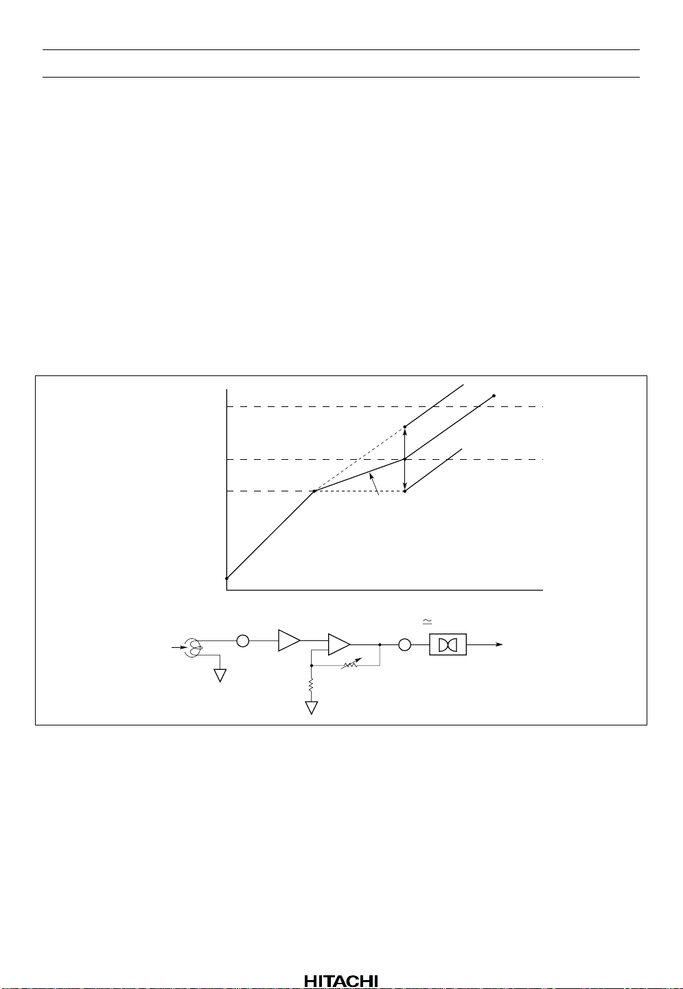
It is the target that total play back output level is adjusted to 3 00mV; Dolby level, which the PB system
gain in all is included of external amplifier’s (Dolby IC etc.) as follows figure 3. Though A head
adjustment is independent of B, select the value of R9, R18 adequately.
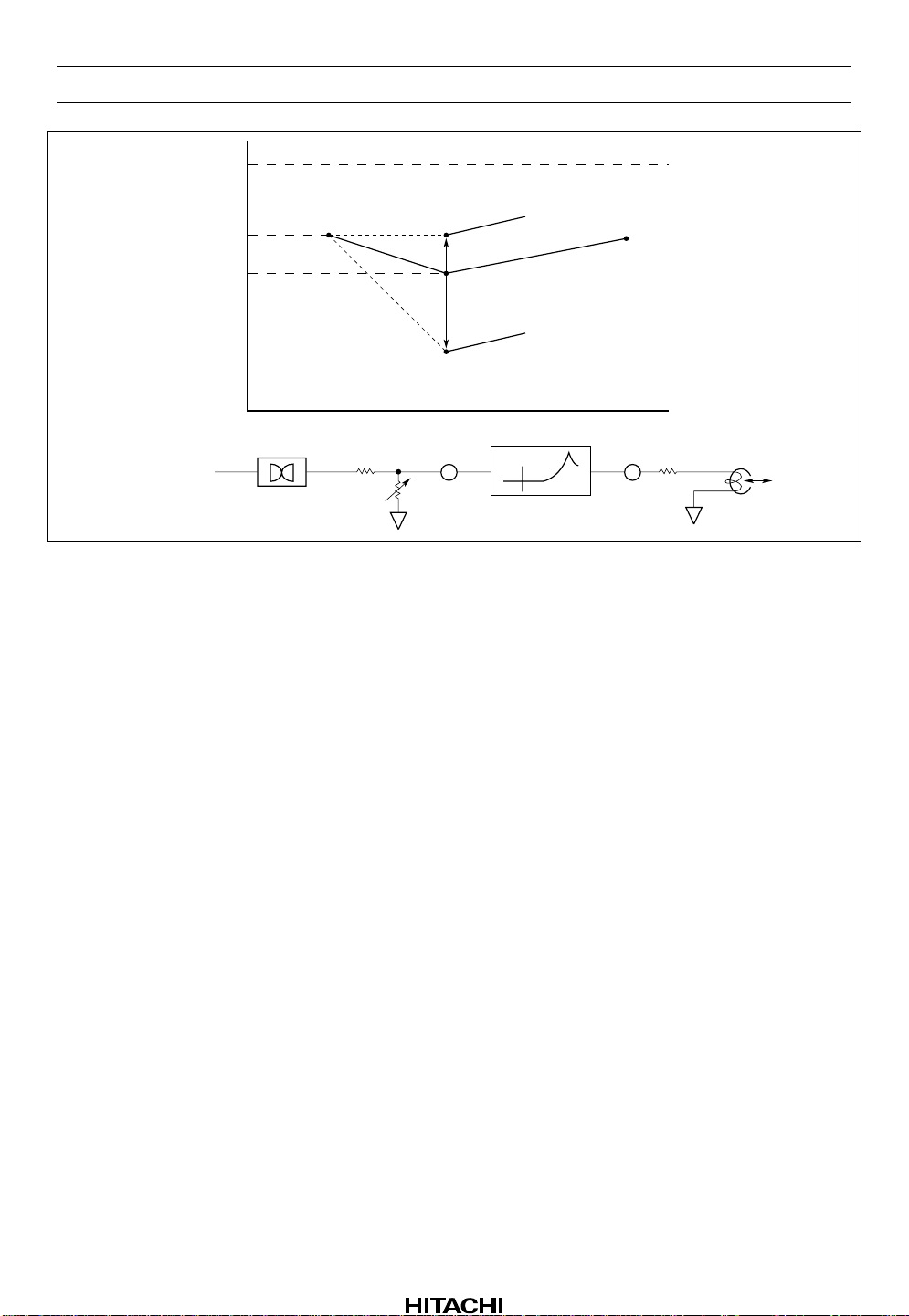
Regarding REC-EQ adjust the gain in front of input to this IC.
The level diagram at 1kHz is shown by figure 4.
Note: 1. R1 needs the valu e mor e than 1kHz.
2. Depending on the employed REC/PB head and test tape characteristics, there is rare case that
the REC-EQ frequency characteristics of this IC can not be matched to the required
characteristics because of built-in resistors which determined the REC-EQ parameters in this
case, please inquire the responsible agent because of the adjustment of built-in resistors is
necessary.
300mV
(Dolby Level)
23.9mV
HA12134A
11.3mV
0.6mV
100kΩ
25.5dB 0 to 20.8dB 20dB
+
–
10kΩ
100kΩ VR
VR = 11kΩ
Dolby IC
Figure 3 PB Level Diagram (Normal Speed, Normal Tape, 1kHz)
Rev.2, Jun. 1997, page 9 of 34
HA12211NT
REC-EQ clip level
1.8V
300mV
(Dolby Level)
100mV
1kHz
Dolby IC
263mV
REC-EQ
Figure 4 REC Level Diagram (Normal Speed, Normal Tape, 1kHz)
5.6kΩ
R1
Rev.2, Jun. 1997, page 10 of 34

HA12211NT
Absolute Maximum Rating (Ta = 25°C)
Item Symbol Rating Unit Note
Max supply voltage V
Power dissipation P
Operating temperature Topr –40 to +75 °C
Storage temperature Tstg –55 to +125 °C
Operating voltage Vopr 9.5 to 15 V
max 16 V
CC
d
500 mW Ta ≤ 75°C
Rev.2, Jun. 1997, page 11 of 34
 Loading...