HIT HA12209F Datasheet

HA12209F
Audio Signal Processor for Cassette Deck
(Dolby B-type NR with Recording System)
ADE-207-221A (Z)
2nd Edition
Jun. 1999
Description
HA12209F is silicon monolithic bipolar IC providing Dolby noise reduction system*, music sensor system,
REC equalizer system and each electronic control switch in one chip.
Functions
• Dolby B-NR × 2 channel
• REC equalizer × 2 channel
• Music sensor × 1 channel
• Each electronic control switch to change REC equalizer, bias, etc.
Features
• REC equalizer is very small number of external parts and have 4 types of frequency characteristics
built-in.
• 2 types of input for PB, 1 type of input for REC.
• 70µ-PB equalizer changing system built-in.
• Dolby NR with dubbing double cassette decks.
Unprocessed signal output available from recording out terminals during PB mode.
• Provide stable music sensor system, available to design music sensing time and level.
• Controllable from direct micro-computer output.
• Bias oscillator control switch built-in.
• NR ON/OFF and REC/PB fully electronic control switching built-in.
• Normal-speed/high-speed, TYPE I/TYPE II and PB equalizer fully electron ic control switching built-in.
• Available to reduce substrate-area because of high integration and small external parts.
* Dolby is a trademark of Dolby Laboratories Licensing Corporation.
A license from Dolby Laboratories Licensing Corporation is required for the use of this IC.

HA12209F
Ordering Information
Standard Level
Operating Voltage
Product Package PB-OUT Level REC-OUT Level Dolby Level Min Max
HA12209F FP-56 580mVrms 300mVrms 300mVrms 10V 15V
Function
Product Dolby B-NR REC-EQ Music Sensor REC/PB Selection
HA12209F ❍❍❍❍
Note: Depending on the employed REC/PB head and test tape characteristics, there is a rare case that the
REC-EQ characteristics of this LSI can not be matched to the required characteristics because of
built-in resistors which determined the REC-EQ parameters in this case, please inquire the
responsible agent because the adjustment of built-in resistor is necessary.
Rev.2, Jun. 1999, page 2 of 49
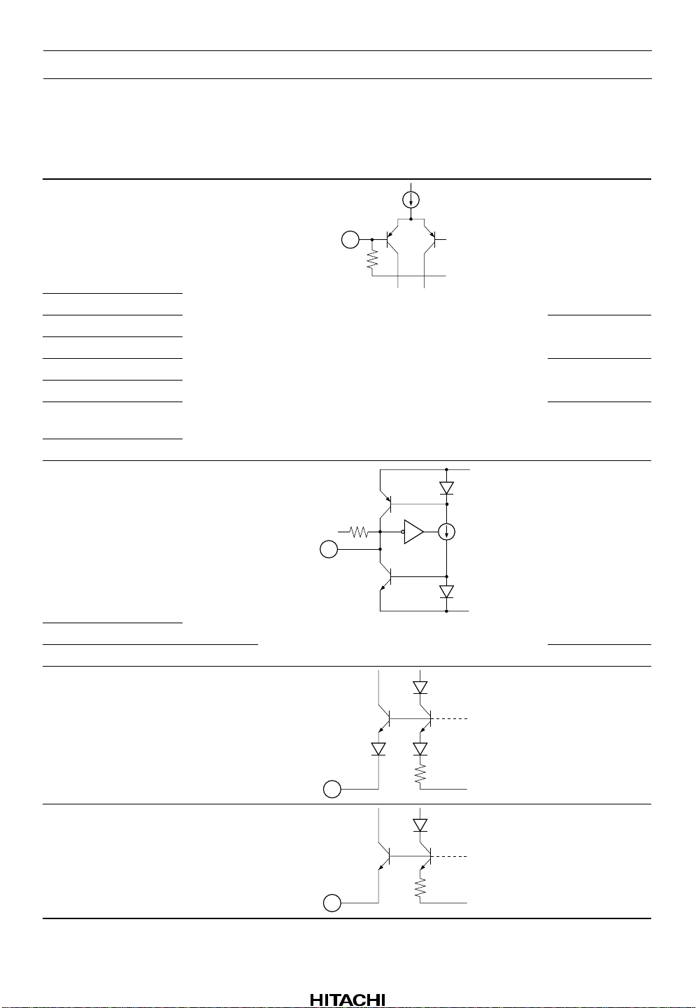
HA12209F
Pin Description, Equivalent Circuit (VCC=12V, Ta=25°C, No signal, The value in the
table show typical value.)
Pin No. Pin Name Note Equivalent Circuit Pin Description
52 AIN (R) V = V
/ 2
CC
V
100k
VCC/2
48 AIN (L)
54 BIN (R) PB B deck input
45 BIN (L)
56 RIN (R) REC input
44 RIN (L)
6 EQIN (R) REC equalizer
37 EQIN (L)
4 DET (R) V = 2.6V
V
CC
PB A deck input
input
Time constant
pin for Dolby-NR
V
GND
39 DET (L)
49 RIP V = VCC / 2 Ripple filter
1 BIAS1 V = 0.6V
Dolby bias
current input
V
42 BIAS2 V = 1.3V
GND
REC equalizer
bias current input
V
GND
Rev.2, Jun. 1999, page 3 of 49
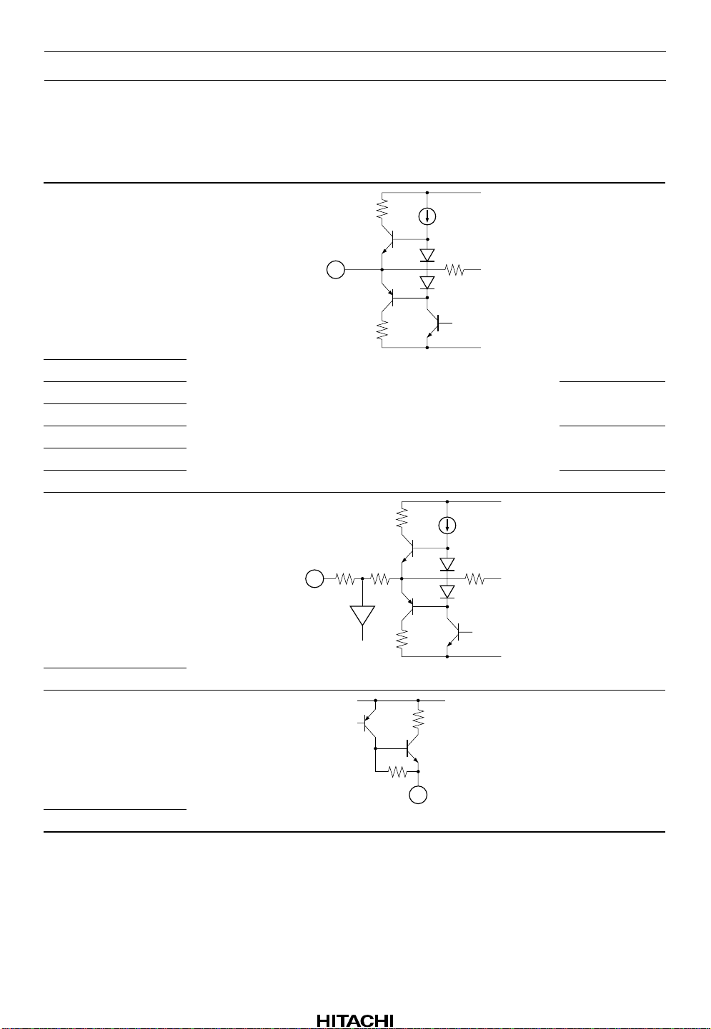
HA12209F
Pin Description, Equivalent Circuit (VCC=12V, Ta=25°C, No signal, The value in the
table show typical value.) (cont)
Pin No. Pin Name Note Equivalent Circuit Pin Description
3 PBOUT (R) V = V
/ 2
CC
V
40 PBOUT (L)
5 RECOUT (R) REC output
38 RECOUT (L)
8 EQOUT (R) Equalizer output
35 EQOUT (L)
32 MAOUT MS amp. input *
53 ABO (R) V = VCC / 2
V
CC
GND
PB output
V
CC
Time constant
pin for PB
equalizer
1
46 ABO (L)
25 BIAS (C) V = VCC –
0.7
26 BIAS (N)
Note: 1. MS : Music Sensor
V
12k15k
GND
V
CC
REC bias current
output
V
Rev.2, Jun. 1999, page 4 of 49
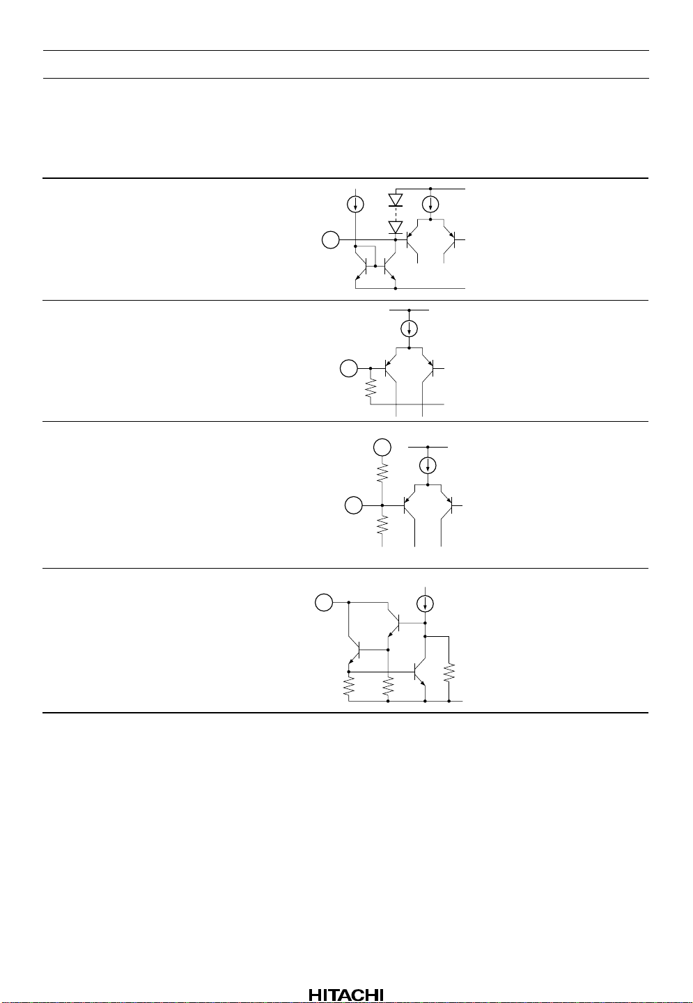
HA12209F
Pin Description, Equivalent Circuit (VCC=12V, Ta=25°C, No signal, The value in the
table show typical value.) (cont)
Pin No. Pin Name Note Equivalent Circuit Pin Description
29 MSDET I = 0µA
31 MSIN V = VCC / 2
V
I
V
V
V
100k
CC
GND
CC
VCC/2
Time constant
pin for MS *
1
MS input
33 MAI V = VCC / 2
27 MSOUT I = 0µA
Note: 1. MS : Music Sensor
MAOUT
V
CC
100k
V
45k
VCC/2
V
CC
V
I
DGND
MS amp. output
MS output (to
MPU)
Rev.2, Jun. 1999, page 5 of 49
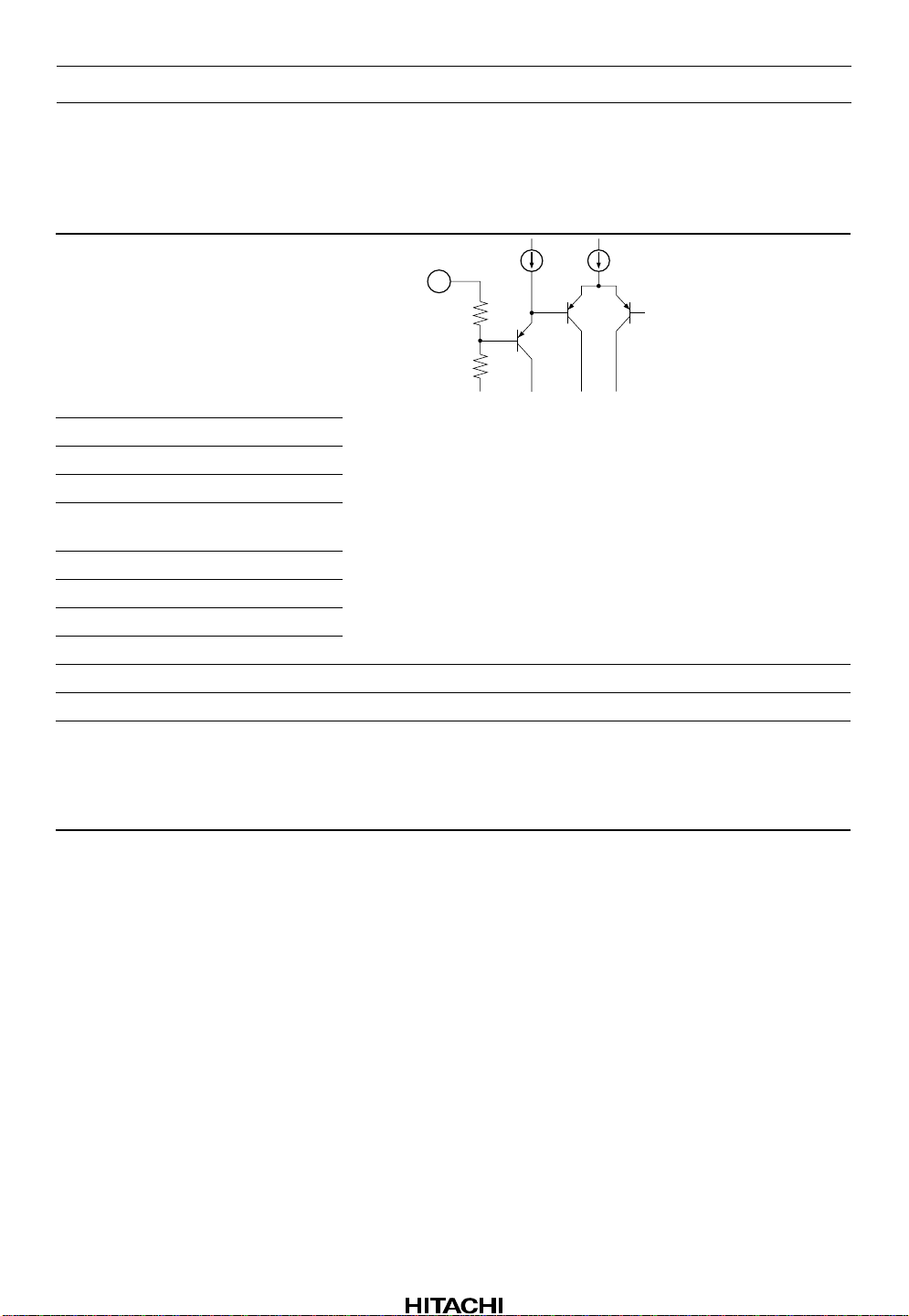
HA12209F
Pin Description, Equivalent Circuit (VCC=12V, Ta=25°C, No signal, The value in the
table show typical value.) (cont)
Pin No. Pin Name Note Equivalent Circuit Pin Description
10 PB A/B I = 20µA
V
22k
100k
I
GND
11 A 120/70
12 NORM/HIGH
14 B 120/70
16 BIAS
ON/OFF
17 RM ON/OFF
19 NR ON/OFF
20 REC/PB
21 LM ON/OFF
22, 23 V
CC
V = V
CC
50, 51 GND V = 0V GND pin
2, 7, 9, 13,
NC No connection
15, 18, 24,
28, 30, 34,
36, 41, 43,
47, 55
Mode control
input
Power supply
Rev.2, Jun. 1999, page 6 of 49
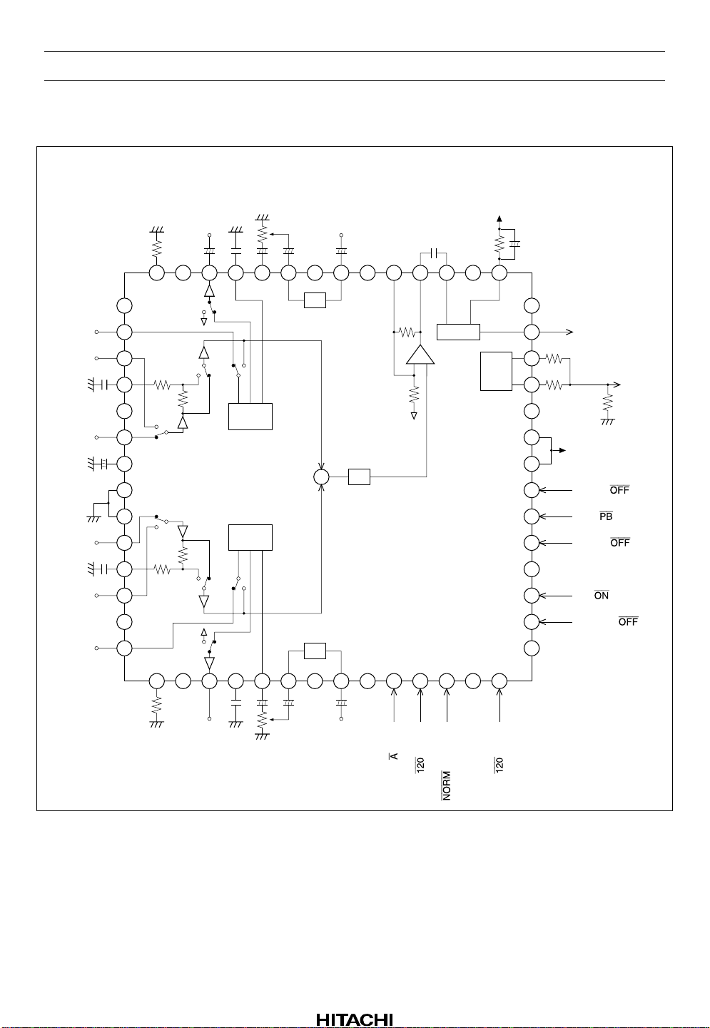
Block Diagram
MAOUT
MAI
NC
EQOUT (L)
NC
EQIN (L)
RECOUT (L)
DET (L)
PBOUT (L)
NC
BIAS2
+
42
41 40 39 38 37 36 35 34 33 32 31 30 29
+
++
MSIN
NC
HA12209F
MSDET
+
NC
RIN (L)
BIN (L)
ABO (L)
NC
AIN (L)
RIP
AIN (R)
ABO (R)
BIN (R)
NC
RIN (R)
43
44
45
15k
46
47
48
49
+
50
51
52
53
54
55
56
12k
12k
15k
1 2 3 4 5 6 7 8 9 10 11 12 13 14
DOLBY
B-NR
DOLBY
B-NR
EQ
+
EQ
+ + +
LPF
45k
100k
–
MS DET
+
BIAS
SW
28
27
26
25
24
23
22
21
20
19
18
17
16
15
NC
MSOUT
BIAS (N)
BIAS (C)
NC
V
CC
LM ON/
REC/
NR ON/
NC
RM /OFF
BIAS ON/
NC
BIASOUT
BIAS1
NC
DET (R)
PBOUT (R)
EQIN (R)
RECOUT (R)
NC
NC
EQOUT (R)
/B
PB
/70
A
/HIGH
B
/70
NC
Rev.2, Jun. 1999, page 7 of 49
HA12209F
Functional Description
Power Supply Range
HA12209F is designed to operate on single supply.
Table 1 Spply Voltage
Item Power Supply Range
Single Supply 10V to 15V
Note: The lower limit of supply voltage depends on the line output reference level.
The minimum value of the overload margin is specified as 12dB by Dolby Laboratories.
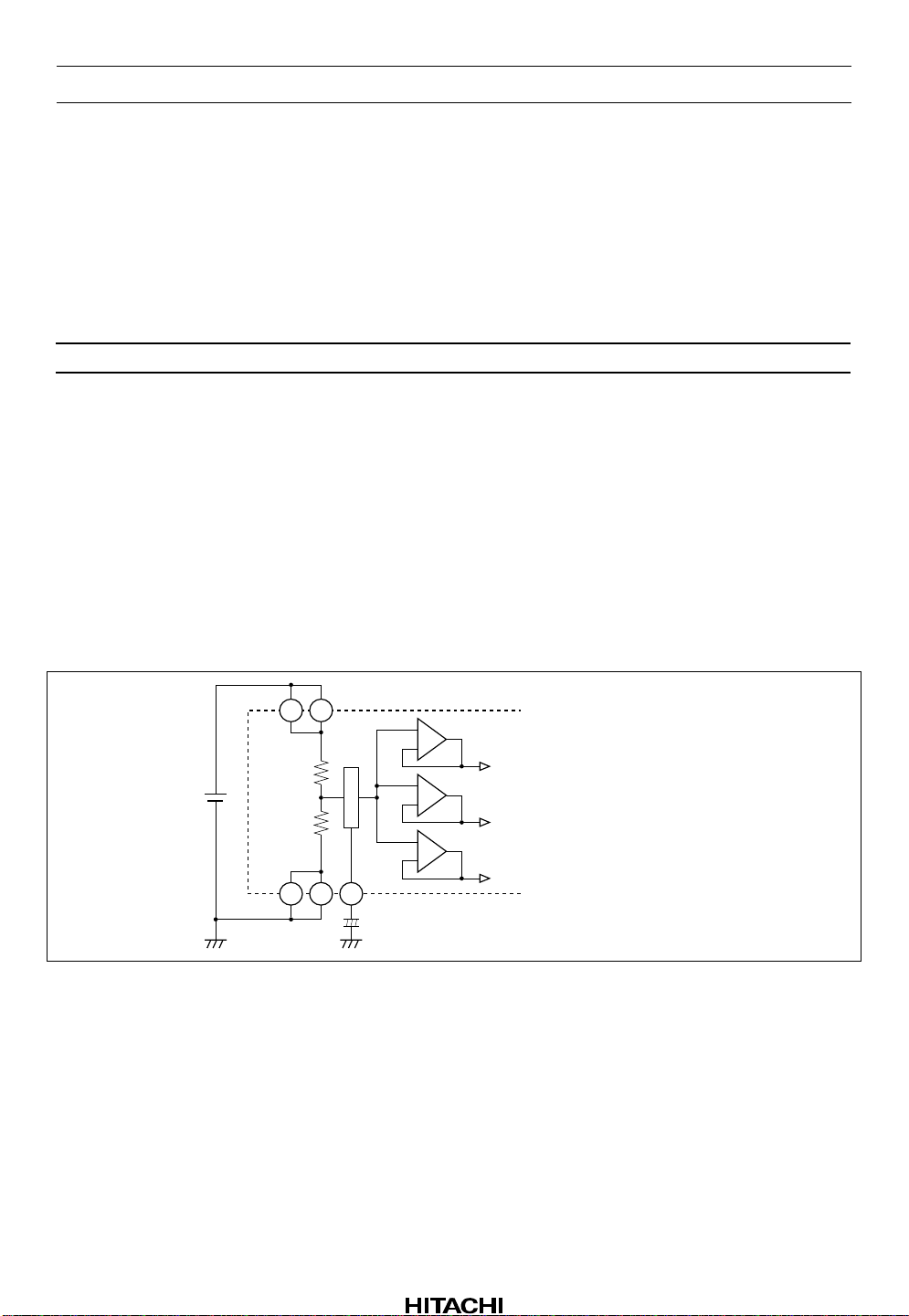
Reference Voltage
For this IC, the reference voltage (V
/2) occurrence device is built-in as AC grand. A capacitor for a
CC
ripple filter is greatly small characteristic with 1/1 00 co mpar ed with co nventional device.
And, the reference voltage are provided for the left channel and the right channel separately.
The block diagram is shown as figure 1.
V
22 23
V
CC
50 51 49
GND PIR
CC
+
–
+
–
+
–
+
1µ
L channel Reference voltage
Music sensor Reference voltage
R channel Reference voltage
Unit
C : F
Figure 1 Reference Voltage
Rev.2, Jun. 1999, page 8 of 49
HA12209F
Operating Mode Control
HA12209F provides fully electronic switching circuits. And each operating mode control is controlled by
parallel data (DC voltage).
Table 2 Control Voltage
Pin No. Lo Hi Unit Test Condition
10, 11, 12, 14, 16,
–0.2 to 1.0 4.0 to 5.3 V
17, 19, 20, 21
Note: 1. Each pins are on pulled down with 100kΩ internal resistor. Therefore, it will be low-level when
each pins are open.
2. Over shoot level and under shoot level of input signal must be the standardized.
(High: 5.3V, Low: –0.2V)
3. For reduction of pop noise, connect 1µF to 22µF capacitor with mode control pins. But it is
impossible to reduce completely in regard to Line mute, therefore, use external mute at the same
time.
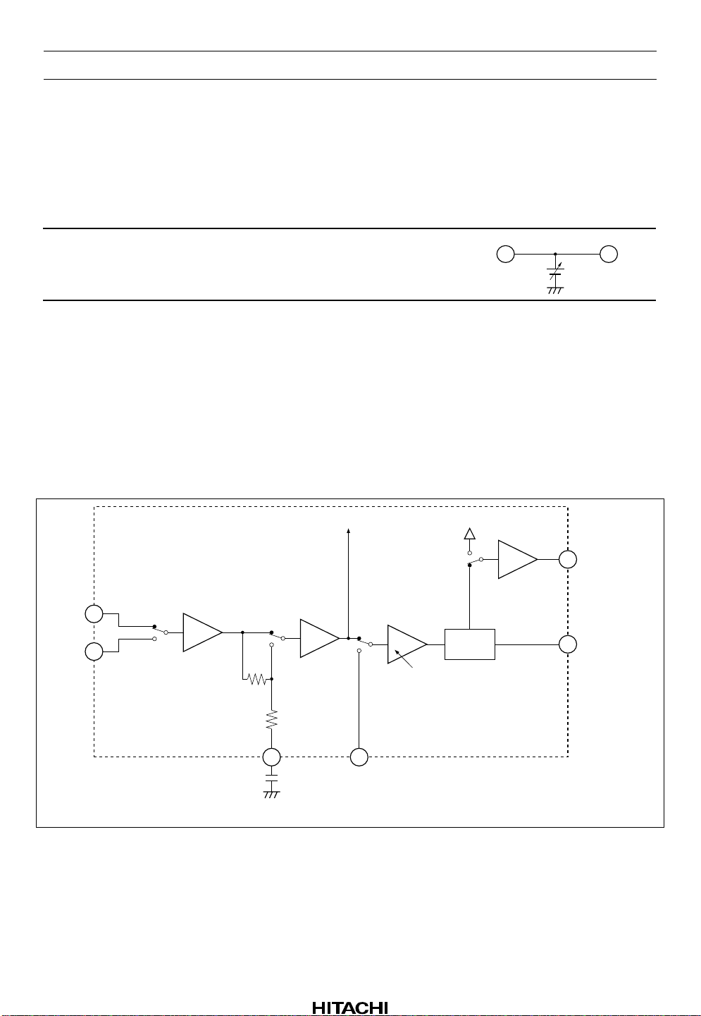
Input Block Diagram and Lev e l Diagram
Input Pin Measure
MS REF
5.7dB
REC
300mVrms
12k
FLAT
(120µ)
70µs
15k
CEX1
0dB
PB
REC
PB/REC=0dB/17dB
42.4mVrmsABO
RIN
AIN
BIN
Note: The each level shown above is typical value when offering PBOUT level to PBOUT pin.
25.9mVrms
21.3dB
300mVrms
PB
300mVrms
DOLBY
B-NR
Figure 2 Input Block Diagram
PBOUT
580mVrms
RECOUT
300mVrms
Unit
R : Ω
C : F
Rev.2, Jun. 1999, page 9 of 49
HA12209F
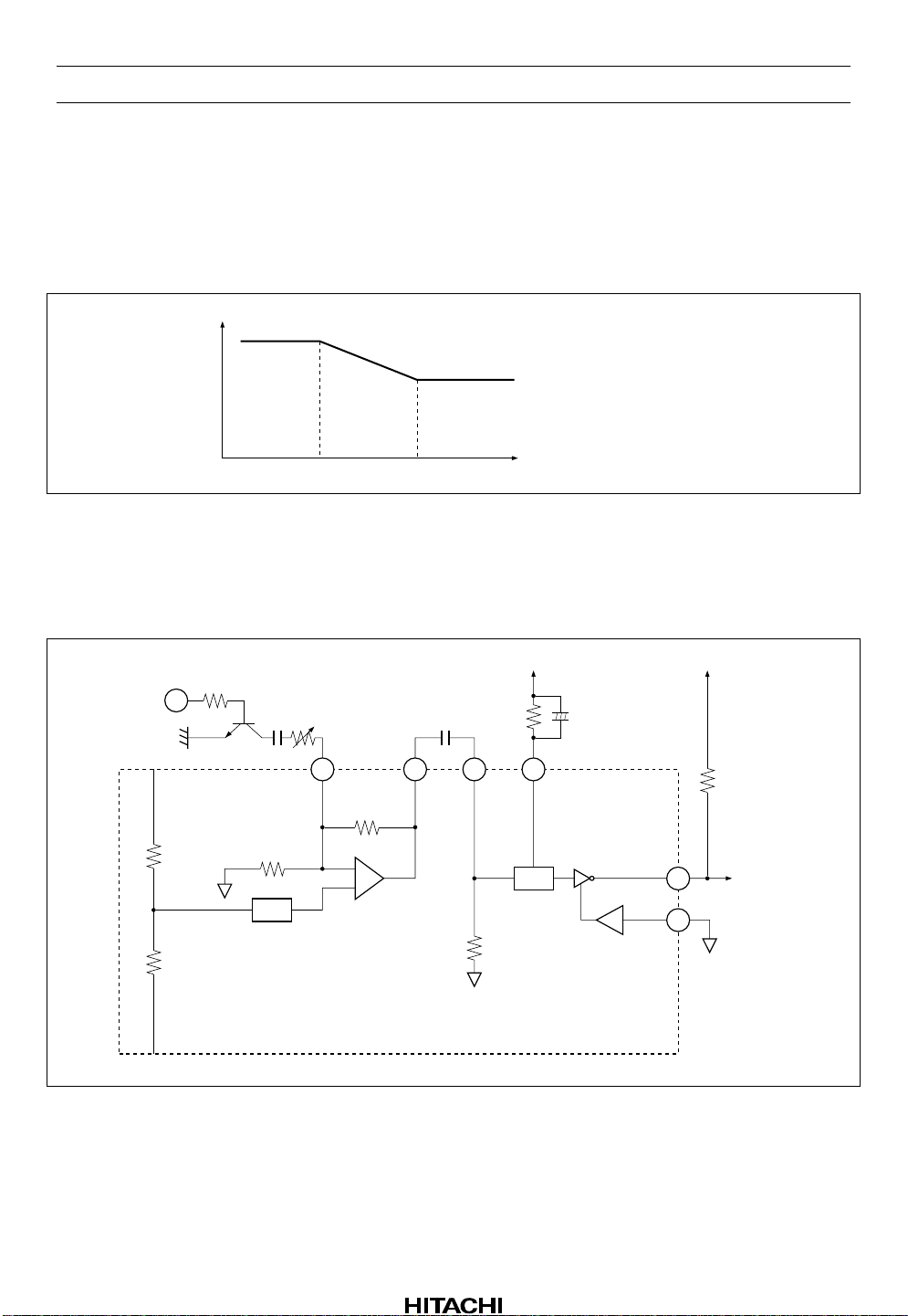
PB Equalizer
By switching logical input level of 11 pin (for Ain) and 14 pin (for Bin), you can equalize corresponding to
tape position at play back mode.
With the capacity CEX1 capacitance that we showed for figure 2 70 µs by the way figure seem to 3 they
are decided.
Gv
t1 = CEX1 · (12k + 15k)
t2 = CEX1 · 15k
(t1) (t2)
Figure 3 Frequency Characteristic of PB Equalizer
The sensitivity Adjustment of Music Sensor
Adjusting MS amp. gain by external resistor, the sensitivity of music sensor can set up.
f
PB(L)
–6dB
PB(R)
REP
45k
LPF
25kHz
MAI
100k
–
+
MS AMP
C26
0.01µ
MA
OUT
R12
330k
MSIN
100k
Figure 4 Music Sensor Block Diagram
V
CC
DET
MS
DET
+
C10
0.33µ
MS OUT
GND
DV
CC
R
L
Microcomputer
GND
Unit
R : Ω
C : F
Rev.2, Jun. 1999, page 10 of 49

The sensitivity of Music Senso r
Gv
HA12209F
f1 =
f2 = 25k [Hz]
f
f1 f2
1
2π · C26 · 100k
[Hz]
Figure 5 Frequency Characteristic of MSIN
Occasion of the external component of figure 4, f1 is 159Hz. A standard level of MS input pin
25.9mVrms, therefore, the sensitivity of music sensor (S) can request it, b y lower formulas.
A = MS Amp Gain
B = PB input Gain × (1/2)*
C = Sensed voltage
20log (A × B) = D [dB]
PB input Gain = 21.3 [dB]
1
S = 20log
S = 14 – D [dB]
C
25.9 · A · B
[dB]
Note: 1. Case of one-sided channel input.
Time Constant of Detection
Figure 6(1) generally shows that detection time is in proportion to value of capacitor C10. But, with
Attack*
2
and Recovery*3 the detection time differs exceptionally.
Recovery
Attack
Detection time
C10
Function Characteristic of MS (1) Function Characteristic of MS (2) Function Characteristic of MS (3)
Recovery Recovery
Attack Attack
Detection time
R12
Detection level
Detection time
Input level
Figure 6 Function Characteristics of MS
Like the figure 6(2), Recovery time is variably possible by value of resistor R12. But Attack time gets
about fixed value. Attack time has dependence by input level. When a large signal is inputted, Attack time
is short tendency.
Note: 2. Attack : Non-music → Music
3. Recovery : Music → Non-music
Rev.2, Jun. 1999, page 11 of 49

HA12209F
Music Sensor Output (MSOUT)
As for internal circuit of music sensor block, music sensor out pin is connected to the collector of NPN type
directly, output level will be “high” when sensing no signal. And ou tput lev el will be “low” when sensing
signal.
Connection with microcomputer, it is requested to use external pull up resistor (R
Note: Supply voltage of MSOUT pin must be less than V
voltage.
CC
= 10k to 22kΩ)
L
The Tolerances of External Components
For Dolby NR precision securing, please use external components shown at figure 7.
If leak-current are a few electrolytic-capacitor, it can be applicable to C2 and C15.
C15
0.1µ
±10%
39
DET (L)
HA12209
BIAS1
R1
33k
±2%
DET (R)
1 4
C2
0.1µ
±10%
Unit
R : Ω
C : F
Figure 7 Tolerance of External Components
Low-Boost
+
CEX2
2.2µ
Vin
Rev.2, Jun. 1999, page 12 of 49
EQIN
REX1
20k
REX2
6.8k
GND
REX3
5.1k
+
CEX3
0.47µ
+
CEX4
0.47µ
REC EQ
Figure 8 Example of Low Boost Circuit
EQOUT
Unit
R : Ω
C : F
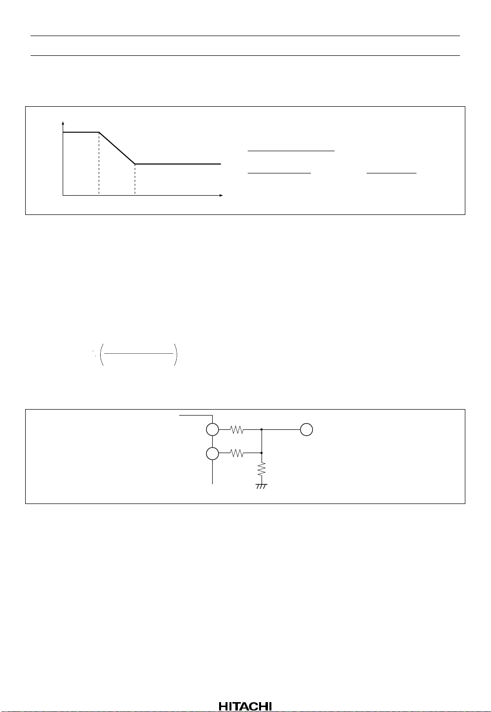
HA12209F
External components shown figure 8 gives frequency response to take 6dB boost. And cut off frequency
can request it, by lower formulas.
Gv
1
1
REX1 · REX2
R0 = [Ω]
REX1 + REX2
f1 f2
f1 = [Hz]
2π · CEX3 · (REX3 + R0)
f2 = [Hz]
2π · CEX3 · REX3
f
Figure 9 Frequency Characteristic of Low-Boost
Bias Switch
This series built-in DC voltage gene rator for bias oscillator and its bias switches.
External resistor R8, R10 which corresponded with tape positions and bias out voltage are relater with
below.
Vbias = × (VCC – 0.7) [V]
R9
(R10 or R8) + R9
Bias switch follows to a logic of 14 pin (B 120/70).
Note: A current that flows at bias out pin, please use it less than 5mA.
BIAS (N)
BIAS (C)
26
25
R10
R8
Vbias
R9
GND
Figure 10 External Components of Bias Block
Rev.2, Jun. 1999, page 13 of 49

HA12209F
Absolute Maximum Rating (Ta=25°C)
Item Symbol Rating Unit Note
Max supply voltage V
Power dissipation P
Operating temperature Topr –40 to +75 °C
Storage temperature Tstg –55 to +125 °C
max 16 V
CC
T
500 mW Ta ≤ 75°C
Rev.2, Jun. 1999, page 14 of 49
HA12209F
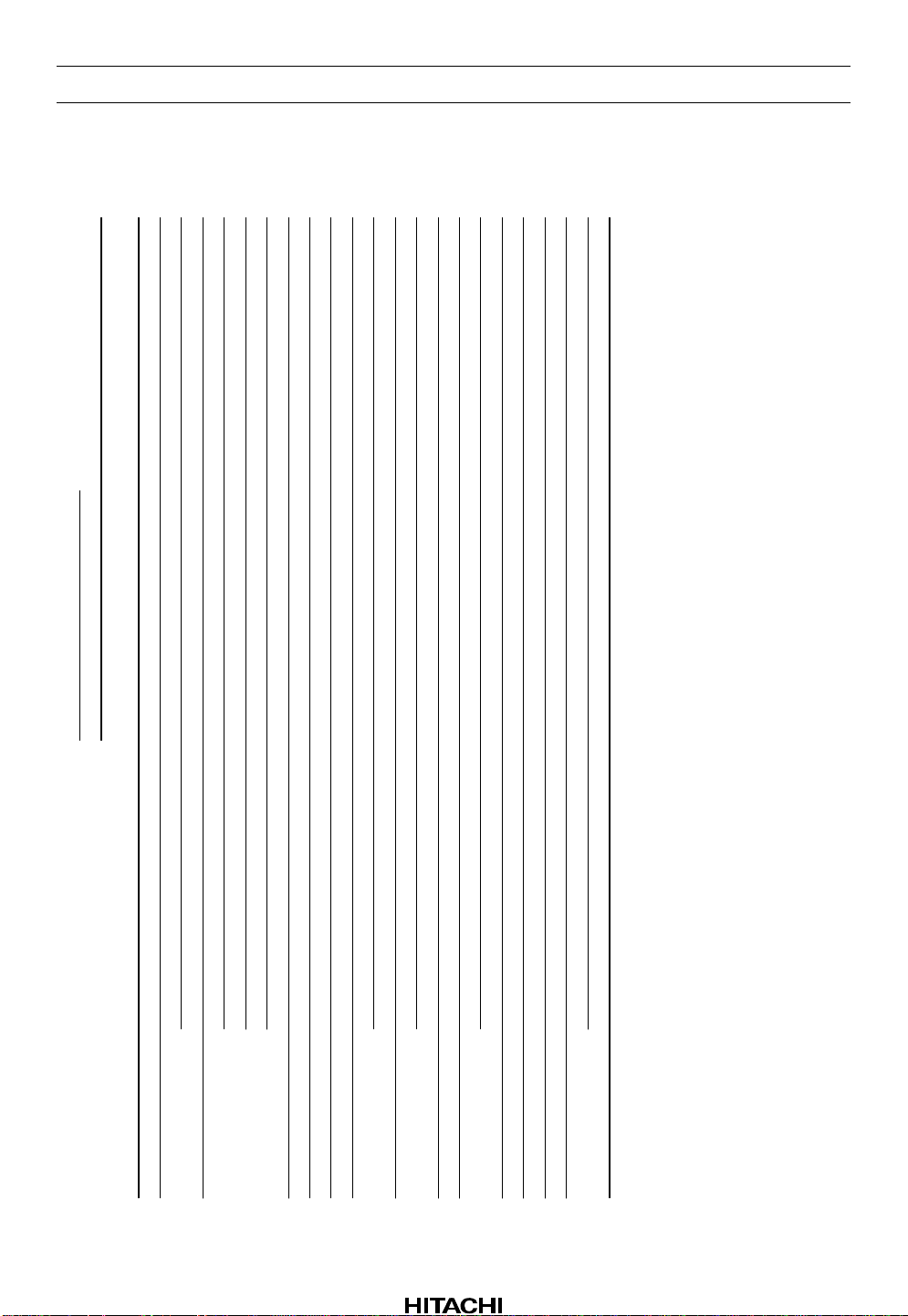
Electrical Characteristics (Ta = 25°C, VCC = 12V, Dolby Level = REC-OUT Level =
300mVrms = 0dB)
2
Other
No signal
RECOUT
level (dB)
——
fin
(Hz)
MUTE
120µ/
120 ON
70µ
–20
0
0
1k1k2k
OFF
OFF
OFF
120
120
120
–30
2k5k5k
OFF
120
THD=1%*
Rg=5.1kΩ, CCIR/ARM
——0
–20
–30
1k1k1k1k1k1k1k
OFF
OFF
120
120
OFF
120
OFF
120
OFF
120
+12
OFF
120
+12
OFF
120
+1200——
+12
+12
1k1k10k5k—
ON
OFF
OFF
1207070
120
120
OFF
OFF
OFF
120
OFF
120
—
—
OFF
120
—
—
—
—
—
—
—
—
1
IC Condition*
A/B
A
A/BAA
REC/PB
NR
PB
PB
ON/OFF
OFF
OFFQuiescent current
mAdBdB
30.0
28.5
23.0
27.0
15.0
25.5
PB
Q
I
G
V
REC
REC
OFF
ON
dB
24.2
5.8
22.7
4.3
21.2
2.8
REC
V
G
ENC 2k (1)
AAA
REC
REC
REC
ON
ON
ON
dBdBdB
10.0
4.7
9.7
8.5
3.2
8.2
7.0
1.7
6.7
ENC 2k (2)
ENC 5k (1)
ENC 5k (2)
AAA
REC
ONONON
dBdB%dBdB
REC
RECPBREC
A/BAA/B
PB
OFF
OFF
OFF
dB
——0.3————
13.0
70.0
0.05
80.0
85.0
70.0
12.0
64.0Ñ70.0
Vo max
S/N
T.H.D.
CTRL (1)
75.0
60.0
CTRL (2)
CT A/B
A
A/B
A/B
REC/PB
OFF
dB
80.0
70.0
CT R/P
A/BAA
PBPBPBPBPB
OFF
OFF
OFF
dBdBdBdBV
—
27.0
23.8
80.0
25.5
22.3
70.0
24.0
20.8
EQ 1k
EQ 10k
V
V
G
MUTE
G
OFF
–7.4
–11.4
–15.4
ONVOL
V
3
OFF
1.5
1.0
—
A
PB
OFF
2.0 µA
—
—
OH
I
—
—
V
1.0
—
–0.2
ILVIH
V
—
—
—
V
5.3
—
4.0
=10V
CC
3. For inputting signal to one side channel
2. V
Item Symbol Min Typ Max Unit Test Condition
B type
Input AMP. gain
Encode boost
Signal handling
Signal to noise ratio
Total harmonic distortion
Channel separation
Crosstalk
Mute attenuation
MS sensing level*
70µ EQ gain
MS output low level
MS output leak current
Note: 1. Other IC condition : REC-MUTE OFF, TYPE I, Normal speed, Bias OFF
Control voltage —
Rev.2, Jun. 1999, page 15 of 49
 Loading...