

HIT 2SC2619 Datasheet
Application
High frequency amplifier
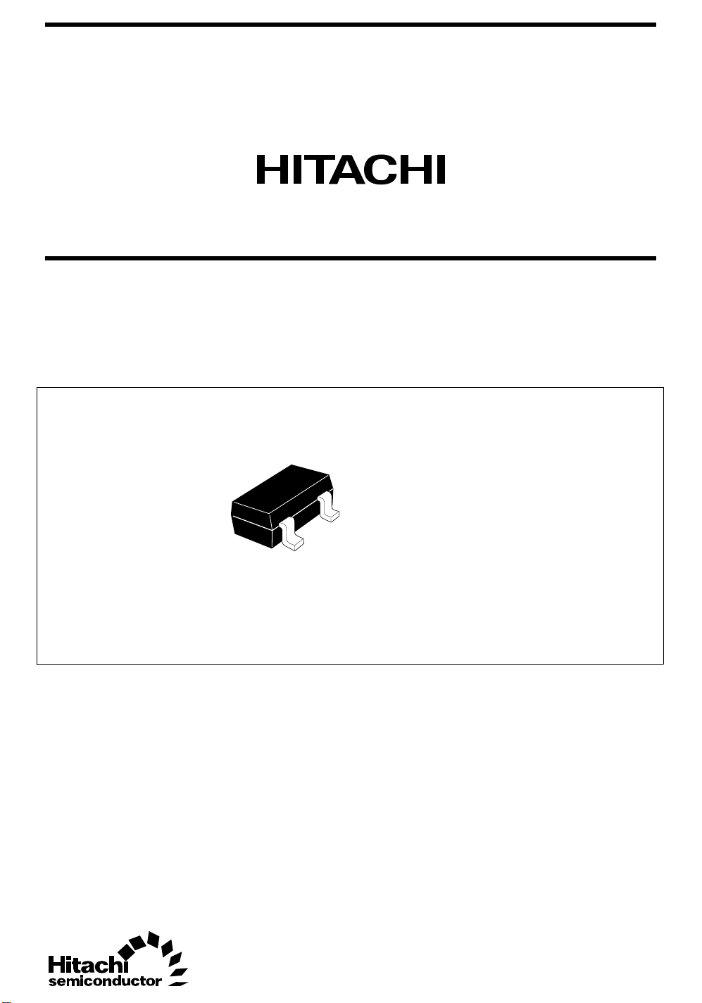
Outline
MPAK
2SC2619
Silicon NPN Epitaxial
3
1
2
1. Emitter
2. Base
3. Collector

2SC2619
Absolute Maximum Ratings (Ta = 25°C)
Item Symbol Ratings Unit
Collector to base voltage V
Collector to emitter voltage V
Emitter to base voltage V
Collector current I
Collector power dissipation P
CBO
CEO
EBO
C
C
Junction temperature Tj 150 °C
Storage temperature Tstg –55 to +150 °C
Electrical Characteristics (Ta = 25°C)
Item Symbol Min Typ Max Unit Test conditions
Collector to base breakdown
V
(BR)CBO
voltage
Collector to emitter breakdown
V
(BR)CEO
voltage
Emitter to base breakdown
V
(BR)EBO
voltage
Collector cutoff current I
Emitter cutoff current I
CBO
EBO
DC current transfer ratio hFE*
Collector to emitter saturation
V
CE(sat)
voltage
Base to emitter voltage V
Gain bandwidth product f
BE
T
Collector output capacitance Cob — — 3.5 pF VCB = 10 V, IE = 0, f = 1 MHz
Noise figure NF — 5.0 — dB VCE = 6 V, IC = 2 mA,
Note: 1. The 2SC2619 is grouped by hFE as follows.
Grade A B C
Mark FA FB FC
h
FE
35 to 75 60 to 120 100 to 200
30 — — V IC = 10 µA, IE = 0
30 — — V IC = 1 mA, RBE = ∞
5——VI
— — 0.5 µAV
— — 0.5 µAV
1
35 — 200 V
— — 1.1 V IC = 10 mA, IB = 1 mA
— — 0.75 V VCE = 12 V, IC = 2 mA
— 230 — MHz VCE = 12 V, IC = 2 mA
30 V
30 V
5V
100 mA
150 mW
= 10 µA, IC = 0
E
= 20 V, IC = 0
CB
= 2 V, IC = 0
EB
= 12 V, IC = 2 mA
CE
f = 1 MHz, R
= 500 Ω
g
See characteristic curves of 2SC460.
2
 Loading...