

HIT 2SC2612 Datasheet
2SC2612
Silicon NPN Triple Diffused
Application
High voltage, high speed and high power switching
Outline
TO-220AB
1. Base
2. Collector
1
2
3
(Flange)
3. Emitter
Absolute Maximum Ratings (Ta = 25°C)
Item Symbol Ratings Unit
Collector to base voltage V
Collector to emitter voltage V
Emitter to base voltage V
Collector current I
Collector peak current I
Base current I
Collector power dissipation PC*
CBO
CEO
EBO
C
C(peak)
B
1
Junction temperature Tj 150 °C
Storage temperature Tstg –55 to +150 °C
Note: 1. Value at TC = 25°C.
500 V
400 V
7V
3A
6A
1.5 A
30 W
2SC2612
Electrical Characteristics (Ta = 25°C)
Item Symbol Min Typ Max Unit Test conditions
Collector to emitter sustain
voltage
Emitter to base breakdown
voltage
Collector cutoff current I
DC current transfer ratio h
Collector to emitter saturation
voltage
Base to emitter saturation
voltage
Turn on time t
Storage time t
Fall time t
Note: 1. Pulse test
V
CEO(sus)
V
CEX(sus)
V
(BR)EBO
CBO
I
CEO
FE1
h
FE2
V
CE(sat)
V
BE(sat)
on
stg
f
400 — — V IC = 0.2 A, RBE = ∞,
L = 100 mH
400 — — V IC = 3 A, IB1 = –IB2 = 0.6 A
V
= –5 V, L = 180 µH,
BE
Clamped
7——VI
= 10 mA, IC = 0
E
— — 100 µAVCB = 400 V, IE = 0
— — 100 µAVCE = 350 V, RBE = ∞
15 — — VCE = 5 V, IC = 1.5 A*
7—— V
= 5 V, IC = 3.0 A*
CE
— — 1.0 V IC = 1.5 A, IB = 0.3 A*
— — 1.5 V IC = 1.5 A, IB = 0.3 A*
— — 1.0 µsI
= 3 A, IB1 = –IB2 = 0.6 A,
C
— 1.2 2.5 µsVCC ≅ 150 V
— — 1.0 µs
1
1
1
1
Maximum Collector Dissipation
Curve
45
(W)
C
30
15
Collector power dissipation P
0 50 100 150
Case temperature T
(°C)
C
Area of Safe Operation
i
10
C(peak)
I
(Continuous)
Cmax
(A)
C
1.0
PW = 10 ms
DC Operation
T
C
= 25°C
0.1
Ta = 25°C, 1 Shot
0.01
Collector current I
0.001
1 3 30 30010 100 1,000
Collector to emitter voltage V
250 µs
1 ms
50 µs
25 µs
CE
(V)
2
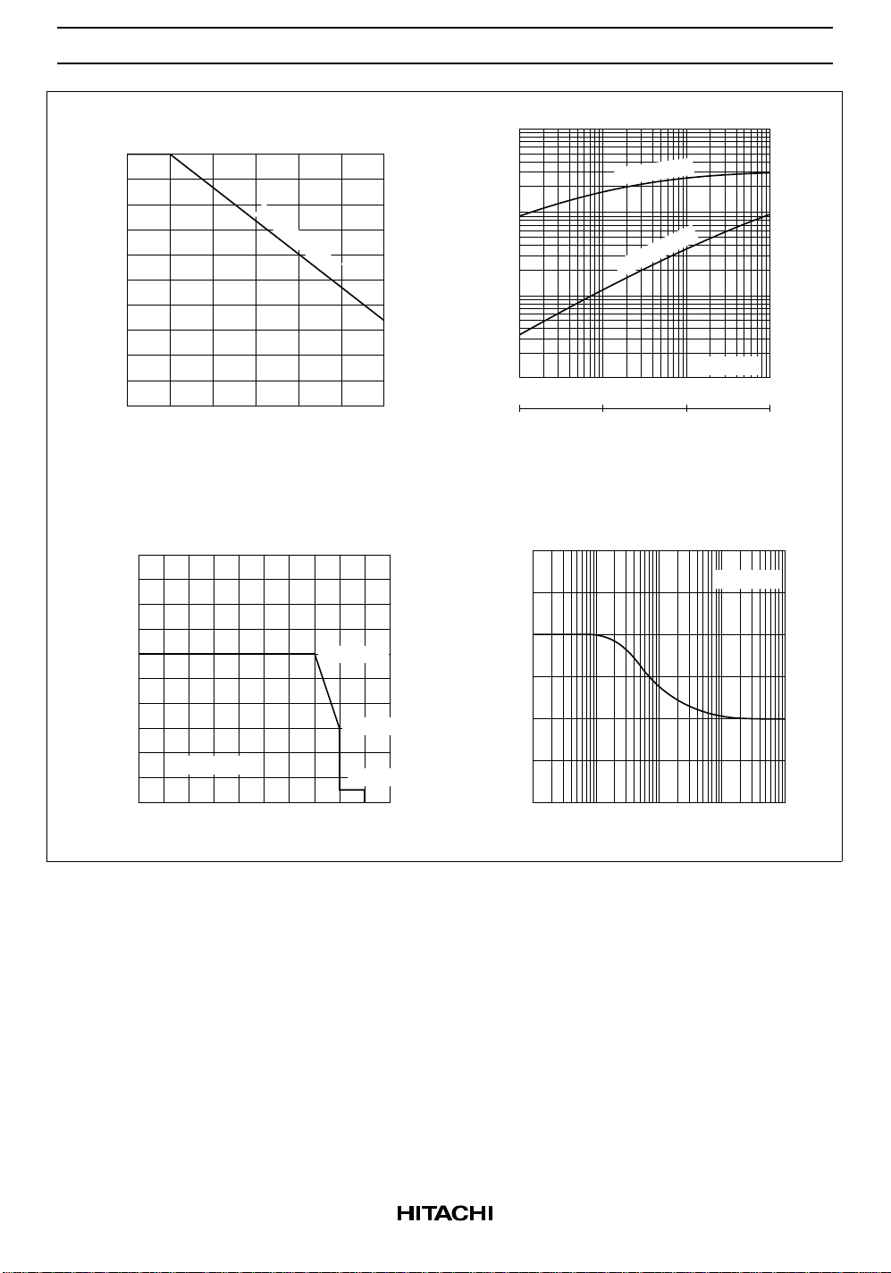
100
80
Collector Current Derating Rate
IS/B Limit Area
(°C/W)
j-c
1.0
Transient Thermal Resistance
10
3
10 ms–10 s
2SC2612
60
40
20
Collector current derating rate (%)
0 50 100 150
Case temperature T
(°C)
C
Reverse Bias Area of Safe Operation
10
8
(A)
C
6
350 V, 6 A
4
Collector current I
2
0 100
IB2 = –0.6 A
200 300 400 500
Collector to emitter voltage VCE (V)
400 V, 3 A
450 V, 0.5 A
0.3
10 µs–10 ms
0.1
0.03
Thermal resistance θ
0.01
TC = 25°C
0.01 0.1 1.0 10 (s)
0.01 0.1 1.0 10 (ms)
Time t
Collector to Emitter Voltage
vs. Base to Emitter Resistance
600
(V)
CER
IC = 1 mA
500
400
Collector to emitter voltage V
300
100 1 k
Base to emitter resistance R
10 k 100 k 1 M
BE
(Ω)
3
 Loading...