

Page 1
harman/kardon
AVR225
A/V DOLBY DIGITAL RECEIVER
SERVICE MANUAL
ESD WARNING………………………….…….2
LEAKAGE TESTING……………….....……....3
BASIC SPECIFICATIONS…………….….…..4
FRONT PANEL CONTROLS………………...5
FRONT PANEL DISPLAY…………………….7
REAR PANEL CONNECTIONS……..….……9
REMOTE CONTROL FUNCTIONS……..…..11
INSTALLATION AND CONNECTIONS….....14
TROUBLESHOOTING GUIDE…………..….16
MICROPROCESSOR RESET……….…..….16
UNIT EXPLODED VIEW………….…..……..17
harman/kardon, Inc.
250 Crossways Park Dr.
Woodbury, New York 11797 Rev5 2/2005
CONTENTS
DISASSEMBLY PROCEDURE..………….18
AMPLIFIER BIAS ADJUSTMENT……...…21
BLOCK DIAGRAM………………………….22
IC PINOUTS……………………………..….23
TRANSISTOR PINOUTS………..…..…….59
ELECTRICAL PARTS LIST………..…..….60
PCB DRAWINGS……………………..……70
SCHEMATICS…………………………...…78
WIRING DIAGRAM..……………………….90
PACKAGING………………………………..91
Page 2
AVR225
2
Some semiconductor (solid state) devices can be damaged easily by static electricity. Such components commonly are called
Electrostatically Sensitive (ES) Devices. Examples of typical ES devices are integrated circuits and some field effect transistors and
semiconductor "chip" components.
The following techniques should be used to help reduce the incidence of component damage caused by static electricity.
1. Immediately before handling any semiconductor component or semiconductor-equipped assembly, drain off any electrostatic charge on
your body by touching a known earth ground. Alternatively, obtain and wear a commercially available discharging wrist strap device,
which should be removed for potential shock reasons prior to applying power to the unit under test.
2. After removing an electrical assembly equipped with ES devices, place the assembly on a conductive surface such as aluminum foil, to
prevent electrostatic charge build-up or exposure of the assembly.
3. Use only a grounded-tip soldering iron to solder or unsolder ES devices.
harman/kardon
4. Use only an anti-static solder removal device. Some solder removal devices not classified as "anti-static" can generate electrical charges
sufficient to damage ES devices.
5. Do not use freon-propelled chemicals. These can generate electrical change sufficient to damage ES devices.
6. Do not remove a replacement ES device from its protective package until immediately before you are ready to install it. (Most replacement
ES devices are packaged with leads electrically shorted together by conductive foam, aluminum foil or comparable conductive material.)
7. Immediately before removing the protective material from the leads of a replacement ES device, touch the protective material to the
chassis or circuit assembly into which the device will be installed.
CAUTION :
8. Minimize bodily motions when handling unpackaged replacement ES devices. (Otherwise harmless motion such as the brushing together
or your clothes fabric or the lifting of your foot from a carpeted floor can generate static electricity sufficient to damage an ES devices.
Be sure no power is applied to the chassis or circuit, and observe all other safety precautions.
Each precaution in this manual should be followed during servicing.
Components identified with the IEC symbol in the parts list are special significance to safety. When replacing a component identified with
, use only the replacement parts designated, or parts with the same ratings or resistance, wattage, or voltage that are designated in the
parts list in this manual. Leakage-current or resistance measurements must be made to determine that exposed parts are acceptably
insulated from the supply circuit before retuming the product to the customer.
Page 3
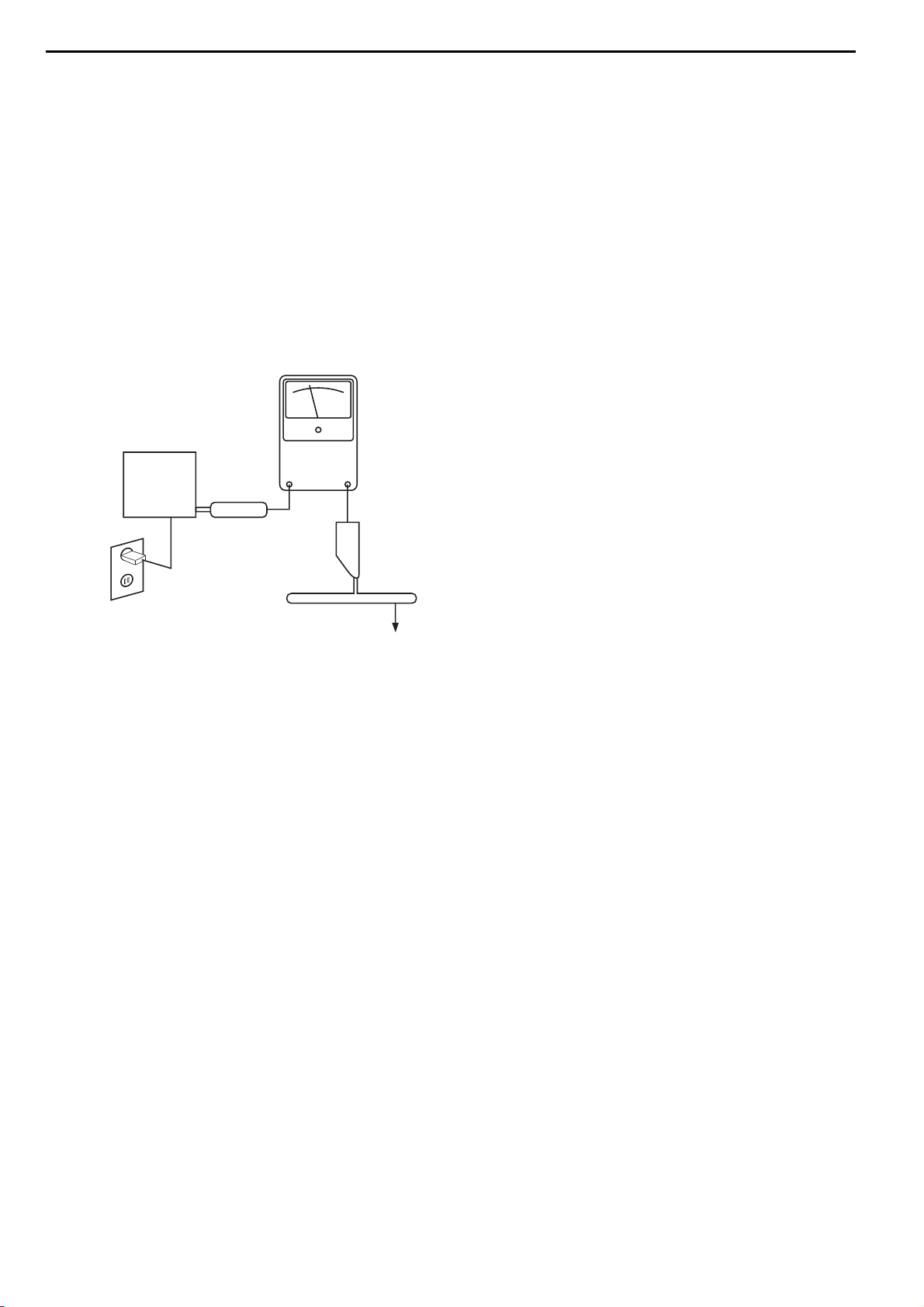
SAFETY PRECAUTIONS
The following check should be performed for the continued
protection of the customer and service technician.
LEAKAGE CURRENT CHECK
Measure leakage current to a known earth ground (water
pipe, conduit, etc.) by connecting a leakage current tester
between the earth ground and all exposed metal parts of the
appliance (input/output terminals, screwheads, metal
overlays, control shaft, etc.). Plug the AC line cord of the
appliance directly into a 120V AC 60Hz outlet and turn the
AC power switch on. Any current measured must not exceed
o.5mA.
ANY MEASUREMENTS NOT WITHIN THE LIMITS
OUTLINED ABOVE ARE INDICATIVE OF A
POTENTIAL SHOCK HAZARD AND MUST BE
CORRECTED BEFORE RETURNING THE APPLIANCE
TO THE CUSTOMER.
AVR225
3
Reading should
not be above
0.5mA
Device
under
test
Leakage
current
tester
harman/kardon
Test all
exposed metal
surfaces
Also test with
plug reversed
(Using AC adapter
plug as required)
Earth
ground
AC Leakage Test
Page 4

Audio Section
Stereo Mode
Continuous Average Power (FTC)
70 Watts per channel, @ < 0.07% THD, 20Hz – 20kHz,
both channels driven into 8 ohms
Five-Channel Surround Modes
Power Per Individual Channel
Front L&R channels:
60 Watts per channel
@ < 0.07% THD, 20Hz–20kHz into 8 ohms
Center channel:
60 Watts @ < 0.07% THD, 20Hz–20kHz into 8 ohms
Surround channels:
60 Watts per channel
@ < 0.07% THD, 20Hz–20kHz into 8 ohms
Input Sensitivity/Impedance
Linear (High-Level) 200mV/47k ohms
Signal-to-Noise Ratio (IHF-A) 95dB
Surround System Adjacent Channel Separation
Analog Source Decoding 45dB
Dolby Digital 55dB
DTS 55dB
Frequency Response
@ 1W (+0dB, –3dB) 10Hz–100kHz
High Instantaneous
Current Capability (HCC) ±28 Amps
Transient Intermodulation
Distortion (TIM) Unmeasurable
Slew Rate 40V/µsec
FM Tuner Section
Frequency Range 87.5–108.0MHz
Usable Sensitivity IHF 1.3 µV/13.2dBf
Signal-to-Noise Ratio Mono/Stereo 70dB/68dB
Distortion Mono/Stereo 0.2%/0.3%
Stereo Separation 40dB @ 1kHz
Selectivity ±400kHz, 70dB
Image Rejection 80dB
IF Rejection 90dB
AM Tuner Section
Frequency Range 520–1720 kHz
Signal-to-Noise Ratio 45dB
Usable Sensitivity Loop 500 µV
Distortion 1kHz, 50% Mod 0.8%
Selectivity ±10kHz, 30dB
Video Section
Television Format NTSC
Input Level/Impedance 1Vp-p/75 ohms
Output Level/Impedance 1Vp-p/75 ohms
Video Frequency
Response 10Hz–8MHz (–3dB)
General
Power Requirement AC 120V/60Hz
Power Consumption 68W idle, 540W maximum
(2 channels driven)
Dimensions (Max)
Width 17.3 inches (440mm)
Height 6.6 inches (168mm)
Depth 15.4 inches (390mm)
Weight 26.9 lb (12.2
kg)
Depth measurement includes knobs, buttons and terminal connections.
Height measurement includes feet and chassis.
All features and specifications are subject to change without notice.
*See the following trademark acknowledgements:
Harman Kardon and Power for the Digital Revolution are registered trademarks
of Harman Kardon, Inc.
is a trademark of Harman International Industries, Inc. (patent no. 5,386,478).
Manufactured under license from Dolby Laboratories. "Dolby", ""Pro Logic" and the Double-D
symbol are registered trademarks of Dolby Laboratories. Confidential Unpublished Works.
©1992–1999 Dolby Laboratories, Inc. All rights reserved.
“DTS” and “DTS Digital Surround” are trademarks of Digital Theater Systems, Inc.
UltraStereo is a trademark of UltraStereo Corp.
VMAx is a registered trademark of Harman International Industries, Inc., and is an
implementation of Cooper Bauck Transaural Stereo under patent license.
Logic 7 is a registered trademark of Lexicon, Inc., a Harman International Company,
and Harman International Industries, Inc.
Crystal is a registered trademark of Cirrus Logic Corp.
SPECIFICATIONS
AVR225
4
harman/kardon
TM
Page 5
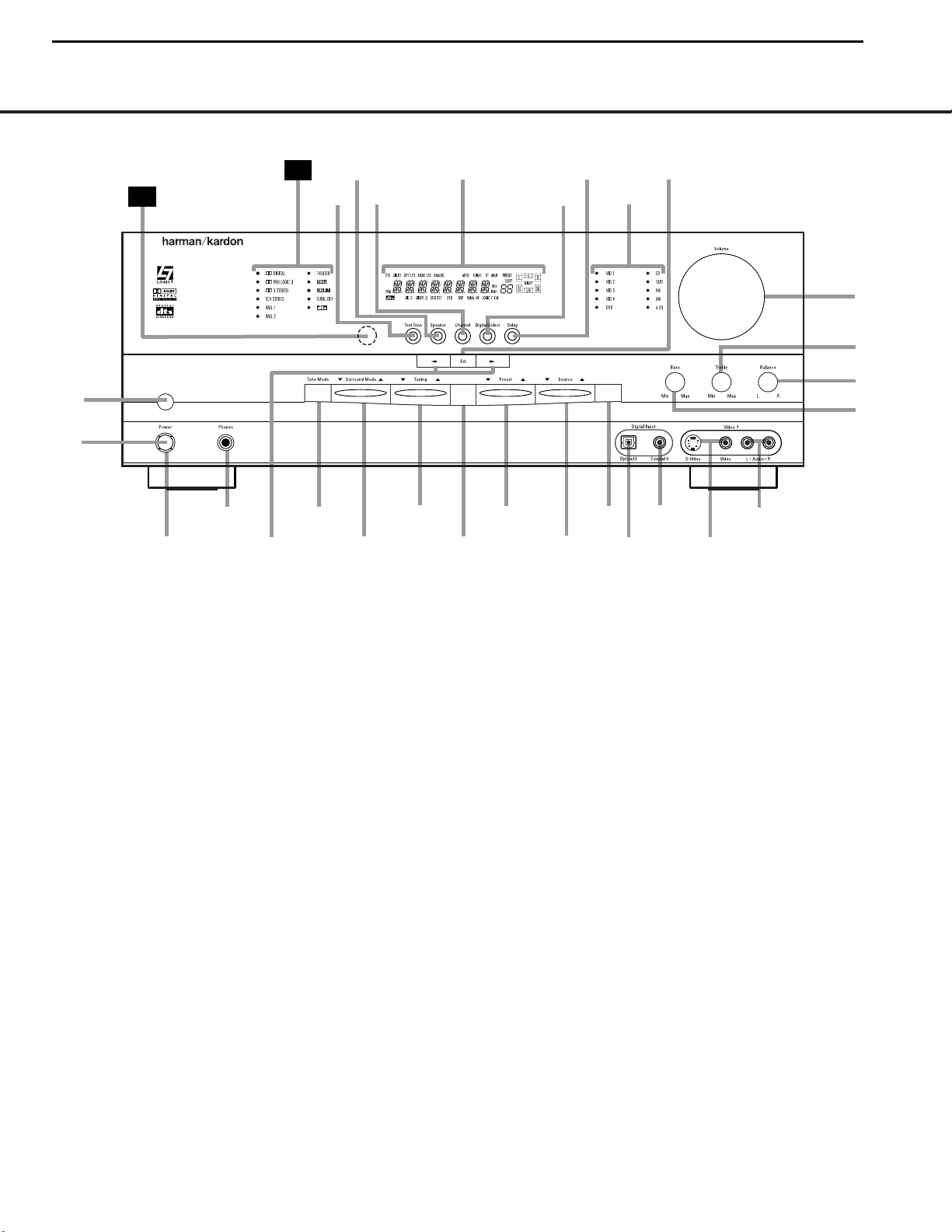
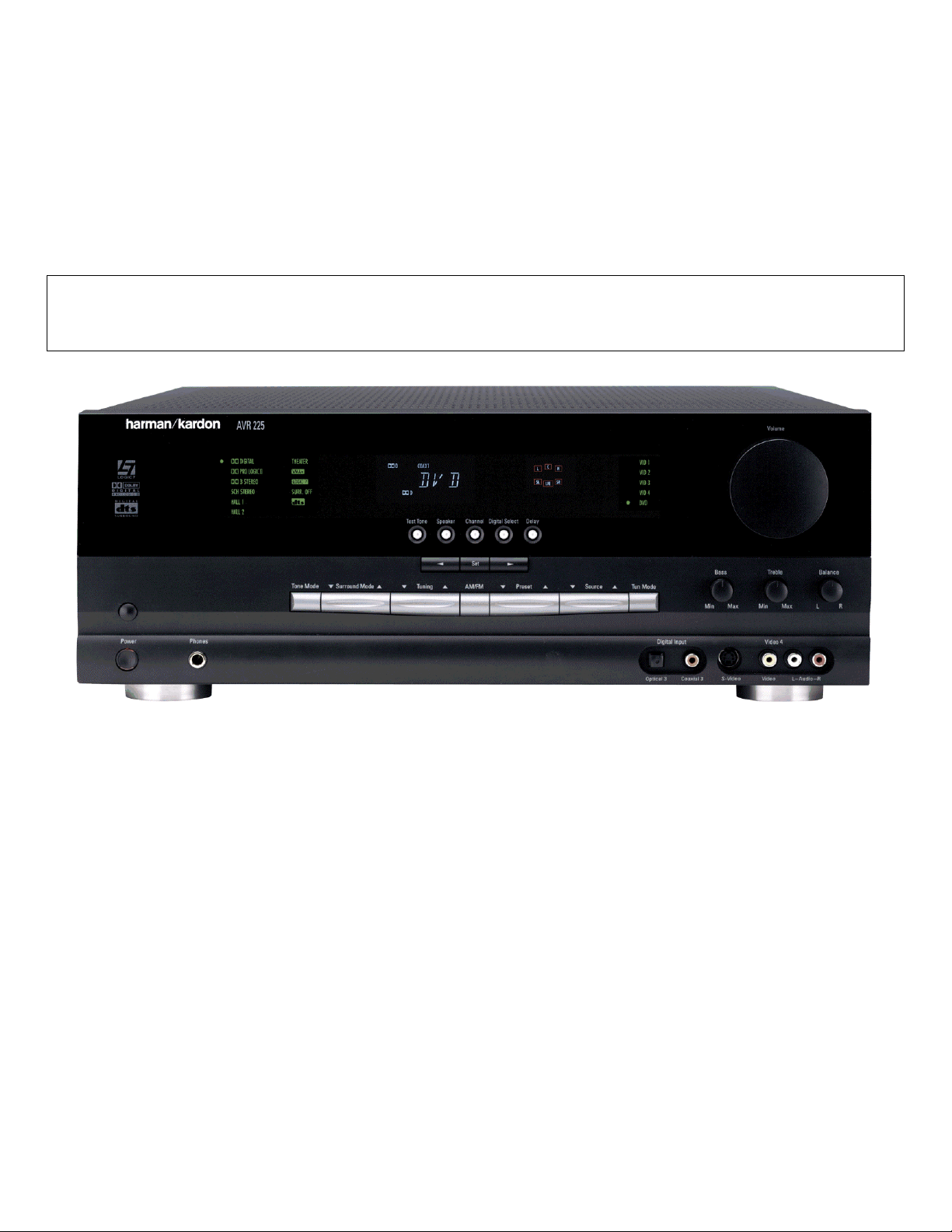
FRONT-PANEL CONTROLS 5
1 Main Power Switch: Press this button to apply
power to the AVR 225.When the switch is pressed
in, the unit is placed in a Standby mode, as indicated
by the amber LED
3 surrounding the System
Power Control
2. This button MUST be pressed in
to operate the unit. To turn the unit off and prevent
the use of the remote control, this switch should be
pressed until it pops out from the front panel so that
the word “OFF” may be read at the top of the switch.
NOTE: This switch is normally left in the “ON” position.
2 System Power Control: When the Main Power
Switch
1
is “ON,” press this button to turn on the
AVR 225; press it again to turn the unit off. Note that
the
Power Indicator3surrounding the switch will
turn green when the unit is on.
3 Power Indicator: This LED will be illuminated in
amber when the unit is in the Standby mode to signal
that the unit is ready to be turned on. When the unit
is in operation, the indicator will turn green. Should
the indicator turn red, turn the unit off using the
Main Power Switch 1 and check the speaker
wire connections to make certain that there are no
short circuits.
4 Headphone Jack: This jack may be used to listen
to the AVR 225’s output through a pair of headphones.
Be certain that the headphones have a standard
1
/4"
stereo phone plug. Note that the main room speakers
will automatically be turned off when the headphone
jack is in use.
5 Selector Buttons: When you are establishing the
AVR 225’s configuration settings, use these buttons to
select from the choices available,
as shown in the Main
Information Display
Û.
6 Tone Mode: Pressing this button enables or dis-
ables the Bass and Treble tone controls. When the
button is pressed so that the words
TONE IN
appear in the Main Information Display Û, the
settings of the
Bass & and Treble ( controls may
be used to adjust the output signals.When the button
is pressed so that the words
TONE OUT appear
in the
Main Information Display Û, the output sig-
nal will be “flat,” without any bass or treble alteration,
no matter how the actual
Bass and Treble Controls
&( are adjusted.
7 Surround Mode Selector: Press this button to
change the surround mode by scrolling through the list
of available modes. Note that depending on the type
FRONT-PANEL CONTROLS
1 Main Power Switch
2 System Power Control
3 Power Indicator
4 Headphone Jack
5 Selector Buttons
6 Tone Mode
7 Surround Mode Selector
8 Tuning Selector
9 AM/FM Selector
) Preset Stations Selector
! Input Source Selector
@ Tuning Mode Selector
# Digital Optical 3 Input
$ Digital Coax 3 Jack
% Video 4 Video Input Jacks
^ Video 4 Audio Input Jacks
& Bass Control
* Balance Control
( Treble Control
Ó Volume Control
Ô Set Button
Input Indicators
Ò Delay
Ú Digital Input Selector
Û Main Information Display
Ù Channel Select Button
ı Speaker Select Button
ˆ Test Tone Selector
˜ Surround Mode Indicators
¯ Remote Sensor Window
4
3
7
8
9
)
!
@
#
$
%
^
*
&
(
Ó
29
6
30
5
AVR 225
Tun Mode
AM/FM
2
1
Ú
ı
Û
Ô
ˆ
Ù
Ò
dB
AVR225
5
harman/kardon
Page 6

6 FRONT-PANEL CONTROLS
FRONT-PANEL CONTROLS
of input, some modes are not always available. (See
page 25 for more information about surround modes.)
8 Tuning Selector: Press the left side of the button
to tune lower-frequency stations and the right side of
the button to tune higher-frequency stations.When a
station with a strong signal is reached, the
Tuned
Indicator
Q will be illuminated in the Main
Information Display
Û.
In Manual tuning mode, tap the button lightly and note
that the tuner will step up one frequency increment per
button press.When the button is held for a few seconds you will note that the unit will quickly advance
through the frequency band. Release it and the tuner
will stop. In Auto tuning mode, each press of the button will search for the next station with an acceptable
signal. Press and hold the button to skip through the
acceptable stations.When the button is released, the
tuner will not stop until it reaches a station with an
acceptable frequency.
To switch back and forth between the Auto and
Manual tuning modes, press the
Tuning Mode
Selector
@.
9 AM/FM Selector: Pressing this button will auto-
matically switch the AVR 225 to the Tuner mode.
Pressing it again will switch between the AM and FM
frequency bands. (See page 28 for more information
on the tuner.)
) Preset Stations Selector: Press this button to
scroll up or down through the list of stations that have
been entered into the preset memory. (See page 28
for more information on tuner presets.)
! Input Source Selector: Press this button to
change the input by scrolling up or down through the
list of input sources.
@ Tuning Mode Selector: Press this button to select
Auto or Manual tuning. When the button is pressed so
that the
Auto Indicator R lights, the tuner will search
for the next station with an acceptable signal when the
Tuning Selector 8u is pressed. When the button
is pressed so that the
Auto Indicator R is not lit,
each press of the
Tuning Selector 8u will
increase the frequency.This button may also be used to
switch between Stereo and Mono modes for FM radio
reception. When weak reception is encountered, press
the button until the
Stereo Indicator P goes out to
switch to Mono reception. Press and hold again to
switch back to Stereo mode. (See page 28 for more
information on using the tuner.)
# Digital Optical 3 Input: Connect the optical digital
audio output of an audio or video product to this jack.
When the input is not in use, be certain to keep the
plastic cap installed to avoid dust contamination that
might degrade future performance.
$ Digital Coax 3 Jack: This jack is used for con-
nection to the output of portable audio devices, video
game consoles or other products that have a coax
digital audio jack.
% Video 4 Video Input Jacks: These jacks may
be used for temporary connection to the composite or
S-Video output of video games, camcorders or other
portable video products.
^ Video 4 Audio Input Jacks: These audio jacks
may be used for temporary connection to video
games or portable audio/video products such as
camcorders and portable audio players.
& Bass Control: Turn this control to modify the lowfrequency output of the left/right channels by as much as
±10dB, when the unit is in the “Surround Off” mode. Set
this control to a suitable position for your taste or room
acoustics.
* Balance Control: Turn this control to change the
relative volume for the front left/right channels.
NOTE: For proper operation of the surround modes
this control should be at the midpoint or “12 o’clock”
position.
( Treble Control:Tu rn this control to modify the high-
frequency output of the left/right channels by as much as
±10dB, when the unit is in the “Surround Off” mode. Set
this control to a suitable position for your taste or room
acoustics.
Ó Volume Control: Tu rn this knob clockwise to
increase the volume, counterclockwise to decrease
the volume. If the AVR 225 is muted, adjusting the
Volume Control Ó will automatically release
the unit from the silenced condition.
Ô Set Button: When making choices during the
setup and configuration process, press this button to
enter the desired setting as shown in the
Main Infor-
mation Display
Û into the AVR 225’s memory. The
Set button may also be used to change the display
brightness (see page 30).
Input Indicators: A green LED will light in front of
the input that is currently being used as the source for
the AVR 225.
Ò Delay: Press this button to begin the sequence
of steps required to enter delay time settings. (See
page 18 for more information on delay times.)
Ú Digital Input Selector: When playing a source
that has a digital output, press this button to select
between the
Optical #e and Coaxial $b
digital inputs or to select the source’s analog input.
(See pages 26–28 for more information on digital
audio.)
Û Main Information Display: This display delivers
messages and status indications to help you operate
the receiver. (See pages 7–8 for a complete explanation of the Information Display.)
Ù Channel Select Button: Press this button to
begin the process of trimming the channel output levels using an external audio source. (For more information on output level trim adjustment, see page 29.)
ı Speaker Select Button: Press this button to
begin the process of configuring the unit to match the
type of speakers used in your listening room. (See
pages 19–21 for more information on speaker setup
and configuration.)
ˆ Test Tone Selector: Press this button to begin
the process of adjusting the channel output levels
using the internal test tone as a reference. (For more
information on output level adjustment, see page 21.)
˜ Surround Mode Indicators: A green LED will
light in front of the surround mode that is currently
in use.
¯ Remote Sensor Window: The sensor behind
this window receives infrared signals from the remote
control. Aim the remote at this area and do not block
or cover it.
AVR225
6
harman/kardon
34
Page 7
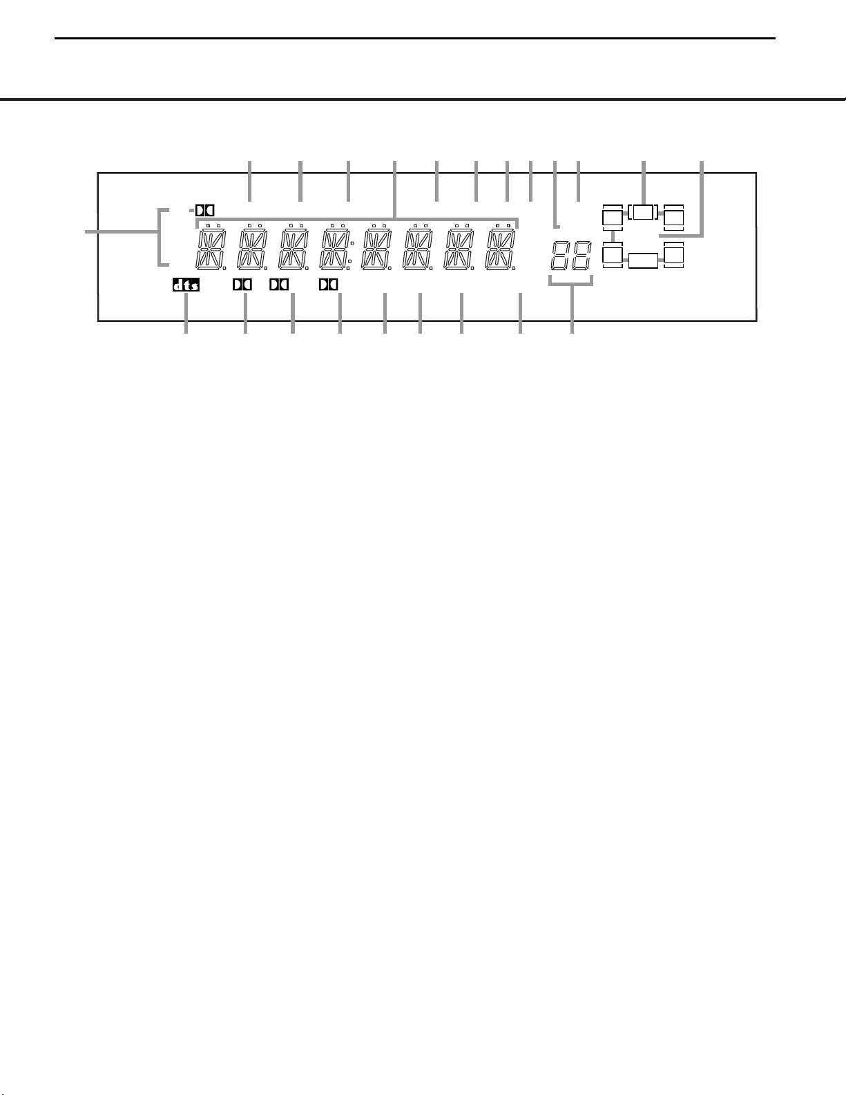
FRONT-PANEL INFORMATION DISPLAY 7
FRONT-PANEL INFORMATION DISPLAY
MEM PRESET
SLEEP
AUTOANALOGCOAX 123OPT 123DTS
PCM
TUNED ST
D PL II 3ST OSD DSP VMAx NF LOGIC 7 CM
KHz
dB
MHz
NIGHT
LR
C
SL SR
LFE
D
A
K
S RTUV Q PO M L
B
C D E F G H I J
N
A Bitstream Indicators
B DTS Mode Indicator
C Dolby Digital Indicator
D Dolby Pro Logic II Indicator
E Dolby 3 Stereo/Stereo Indicator
F OSD Indicator
G DSP Mode Indicator
H VMAx Mode Indicators
I Logic 7 Mode Indicators
J Preset Number/Sleep Timer
K Night Mode Indicator
L Speaker/Channel Input Indicators
M Preset Indicator
N Sleep Indicator
O Memory Indicator
P Stereo Indicator
Q Tuned Indicator
R Auto Indicator
S Main Information Display
T Analog Input Indicator
U Coaxial Digital Input Indicators
V Optical Digital Input Indicators
A Bitstream Indicators: When the input is a digital
source, one of these indicators will light to display the specific type of data signal in use.
B DTS Mode Indicator: This indicator lights when a
DTS-encoded source is playing and DTS Surround
decoding is in use.
C Dolby Digital Indicator: This indicator lights
when a Dolby Digital source is being played and Dolby
Digital surround decoding is in use.
D Dolby Pro Logic II Indicator: This indicator lights
when the Dolby Pro Logic II mode has been selected.
• It is possible to see the Dolby Pro Logic II indicator
lit simultaneously with the Dolby Digital indicator,
even though the Dolby Digital surround mode has
been selected. This is due to the specifications for
Dolby Digital pro
cessing, which require that the Dolby
Pro Logic II
mode be used any time a two-channel
Dolby signal is detected.
• If you desire 5.1-channel audio, check the audio
settings in the menus for both your DVD player and
your DVD disc to make sure that a 5.1-channel
Dolby Digital soundtrack is available and has been
selected.
E Dolby 3 Stereo/Stereo Indicator: The entire
indicator lights when the Dolby 3 Stereo mode has
been selected. When the surround modes are turned
off so that two-channel stereo playback is in use, only
the “ST” indicator will light.
F OSD Indicator: When the On Screen Display
(OSD) system is in use, this indicator lights to remind
you that the other indicators in this display do not
function when the OSD is being used.
G DSP Mode Indicator: This indicator lights when
any of the surround modes created by Digital Signal
Processing, or DSP, are in use. These modes include
Hall 1, Hall 2, the Theater Mode and 5-Channel
Stereo.
H VMAx Mode Indicators: These
light when the
VMAx mode is in use.
VMAx F
appears when the
Far Field VMAx mode is selected;
VMAx N appears
when the Near Field VMAx mode is selected. (See
page 25 for a description of the VMAx modes.)
I Logic 7 Mode Indicators: These indicators light
when the Logic 7 mode is in use.
LOGIC 7C
appears for the Cinema version; LOGIC 7M
appears for the Music version of Logic 7. (See page
25 for a description of the Logic 7 modes.)
J Preset Number/Sleep Timer: When the tuner is
in use, these numbers indicate the specific preset
memory location in use. (See page 28 for more information on preset stations.) When the Sleep function is
in use, these numbers show how many minutes
remain before the unit goes into the Standby mode.
(See page 24 for information on the Sleep function.)
K Night Mode Indicator: This lights when the
AVR 225 is in the Night mode, which preserves the
dynamic range of digital program material at low volume levels.This mode is only available with specially
encoded Dolby Digital sources. (See page 27 for a
description of the Night mode.)
L Speaker/Channel Input Indicators: These indica-
tors are multipurpose, indicating either the speaker type
selected for each channel or the incoming data-signal
configuration. The left, center, right, right surround and
left surround speaker indicators are composed of three
boxes, while the subwoofer is a single box. The center
box lights when a “Small” speaker is selected, and the
two outer boxes light when “Large” speakers are
selected. When none of the boxes are lit for the center,
surround or subwoofer channels, no speaker has been
assigned to one of those positions. (See page 19 for
more information on configuring speakers.) The letters
inside each of the center boxes display active input
channels. For standard analog inputs, only the L and R
will light, indicating a stereo input. When a digital source
is playing, the indicators will light to display the channels
being received at the digital input. When the letters
flash, the digital input has been interrupted. (See page
27 for more information on the Channel Indicators.)
M Preset Indicator: This indicator lights when the
tuner is in use to show that the
Preset Number/
Sleep Timer
J is showing the station’s preset
memory number. (See page 28 for more information
on tuner presets.)
AVR225
7
harman/kardon
Page 8

8FRONT-PANEL INFORMATION DISPLAY
FRONT-PANEL INFORMATION DISPLAY
N Sleep Indicator: This indicator lights when the
Sleep function is in use.The numbers in the
Preset
Number/Sleep Timer
J will show the minutes
remaining before the AVR 225 goes into the Standby
mode. (See page 24 for more information on the Sleep
function.)
O
Memory Indicator: This indicator flashes when
entering presets and other information into the tuner’s
memory.
P Stereo Indicator: This indicator lights when an FM
station is being tuned in stereo.This indicator differs from
the indicator that lights when the surround decoding
modes are turned off, which is described above as the
Dolby 3 Stereo/Stereo Indicator E.
Q
Tuned Indicator:
This indicator lights when a station
is being received with sufficient signal strength to provide acceptable listening quality.
R Auto Indicator: This indicator lights when the
tuner’s Auto mode is in use.
S Main Information Display: This display shows
messages relating to the status, input source, surround
mode, tuner, volume level or other aspects of the
AVR 225’s operation.
T Analog Input Indicator: This indicator lights when
an analog input source has been selected.
U Coaxial Digital Input Indicators: These indicators
light to show when a coaxial digital audio input has
been selected.
V Optical Digital Input Indicators: These indicators
light to show when an optical digital audio input has
been selected.
NOTE: See page 26 for information on assigning either
an analog input or one of the digital audio inputs to the
source currently in use.
AVR225
8
harman/kardon
Page 9

REAR-PANEL CONNECTIONS 9
REAR-PANEL CONNECTIONS
‚¤‹ fi
·
a
b
c
d
f
g
h
i
j
k
•
ª ⁄
›
38
39
40
41
31
37
36
35
34
33
32
fl
‡
°
e
™
¢
∞
£
§
¶
¡
SURR SURR
, 0.5A
, 1A
¡ AM Antenna
™ FM Antenna
£ CD Inputs
¢ Tape Outputs
∞ Tape Inputs
§ Remote IR Input
¶ Remote IR Output
• Subwoofer Output
ª Front Right Speaker Outputs
‚ Surround Right Speaker Outputs
⁄ Center Speaker Outputs
¤ Surround Left Speaker Outputs
‹ Front Left Speaker Outputs
› Switched AC Accessory Outlet
fi Unswitched AC Accessory Outlet
fl AC Power Cord
‡ Optical Digital Audio Output
° Coaxial Digital Audio Output
· Video Monitor S-Video Output
a DVD S-Video Input
b Coaxial Digital Audio Inputs
c Video 1 S-Video Input
d Video 1 S-Video Output
e Optical Digital Audio Inputs
f Video 2 S-Video Input
g Video 2 S-Video Output
h Video 3 S-Video Input
i 6-Channel Direct Inputs
j Video Monitor Composite Video Output
k DVD Composite Video Input
DVD Audio Inputs
Video 1 Composite Video Input
Video 1 Audio Inputs
Video 1 Composite Video Output
Video 1 Audio Outputs
Video 2 Composite Video Input
Video 2 Audio Inputs
Video 2 Composite Video Output
Video 2 Audio Outputs
Video 3 Composite Video Input
Video 3 Audio Inputs
¡ AM Antenna: Connect the AM loop antenna sup-
plied with the receiver to these terminals. If an external
AM antenna is used, make connections to the
AM and
GND terminals in accordance with the instructions
supplied with the antenna.
™ FM Antenna: Connect the supplied indoor (or an
optional external) FM antenna to this terminal.
£ CD Inputs: Connect these jacks to the output of
a compact disc player or CD changer.
¢ Ta pe Outputs: Connect these jacks to the
RECORD/INPUT jacks of an audio recorder.
∞ Tape Inputs: Connect these jacks to the
PLAY/OUT jacks of an audio recorder.
§ Remote IR Input: If the AVR 225’s front-panel
IR sensor is blocked due to cabinet doors or other
obstructions, an external IR sensor may be used.
Connect the output of the sensor to this jack.
¶ Remote IR Output: This connection permits the
IR sensor in the receiver to serve other remotecontrolled devices. Connect this jack to the “IR IN” jack
on Harman Kardon (or other compatible) equipment.
• Subwoofer Output: Connect this jack to the line-
level input of a powered subwoofer. If an external sub-
woofer amplifier is used, connect this jack to the subwoofer amplifier input.
ª⁄‹ Front Speaker Outputs: Connect these
outputs to the matching + or – terminals on your front
speakers.When making speaker connections, always
make certain to maintain correct polarity by connecting
the black terminal to the negative (–) terminal on the
speakers. Connect the white terminal to the positive
(+) terminal on the left front speaker, the red terminal
to the positive (+) terminal on the right front speaker
and the green terminal to the positive (+) terminal on
the center front speaker. Newer speakers may have
matching color terminals in accordance with the new
AVR225
9
harman/kardon
31
32
33
34
35
36
37
38
39
40
41
Page 10

10 REAR-PANEL CONNECTIONS
REAR-PANEL CONNECTIONS
CEA specifications, while existing speakers typically
use a red terminal for the positive (+) speaker wire
connection. (See page 14 for more information on
speaker polarity.)
‚¤ Surround Speaker Outputs: Connect these
outputs to the matching + or – terminals on your left
and right surround speakers.When making speaker
connections always make certain to maintain correct
polarity by connecting the black terminal to the negative (–) terminal on the speakers. Connect the blue
terminal to the positive (+) terminal on the left surround speaker and the gray terminal to the positive
(+) terminal on the right surround speaker. Newer
speakers may have matching color terminals in accordance with the new CEA specifications, while existing
speakers typically use a red terminal for the positive
(+) speaker wire connection. (See page 14 for more
information on speaker polarity.)
› Switched AC Accessory Outlet: This outlet may
be used to power any device you wish to have turned
on or off at the same time as the AVR 225. Any device
connected to this outlet will be off when the AVR 225
is in the Standby mode, and power will be supplied to
the outlet when the AVR 225 is turned on.
fi Unswitched AC Accessory Outlet: This outlet
may be used to power any AC device. The power will
remain on at this outlet regardless of whether the
AVR 225 is on or off.
NOTE: The total power consumption of all devices
connected to the accessory outlets should not exceed
100 watts. Do not connect power amplifiers or other
high-current draw devices to these outlets.
fl AC Power Cord: Connect the AC plug to an
unswitched AC wall outlet.
‡ Optical Digital Audio Output: Connect this jack
to the matching digital audio input connector on a
digital recorder such as a CD-R or MiniDisc recorder.
° Coaxial Digital Audio Output: Connect this jack
to the matching digital audio input connector on a
digital recorder such as a CD-R or MiniDisc recorder.
·j Video Monitor Outputs: Connect these jacks
to the composite or S-Video input of a TV monitor or
video projector to view the on-screen menus and the
output of any standard video source selected by the
receiver’s video switcher.
ak DVD Video Inputs: Connect one of these jacks
to the composite or S-Video output jacks on a DVD or
other video source.
b Coaxial Digital Audio Inputs: Connect the coax
digital audio output from a DVD player, HDTV receiver,
LD player, satellite receiver, cable box, MiniDisc recorder
or CD player to these jacks.The signal may be either a
Dolby Digital signal, DTS signal or a standard PCM digital
source. Do not connect the RF digital output of an
LD player to these jacks.
c Video 1 Video Inputs: Connect one of these
jacks to the
PLAY/OUT composite or S-Video jacks
on a VCR or other video source.
d Video 1 Video Outputs: Connect one of
these jacks to the
RECORD/INPUT composite or
S-Video jack on a VCR.
e Optical Digital Audio Inputs: Connect the optical
digital audio output from a DVD player, HDTV receiver,
LD player, satellite receiver, cable box, MiniDisc player
or recorder, or CD player to these jacks. The signal
may be either a Dolby Digital signal, a DTS signal or a
standard PCM digital source.
f Video 2 Video Inputs: Connect one of these
jacks to the
PLAY/OUT composite or S-Video jacks
on a TV,VCR or other video source.
g Video 2 Video Outputs: Connect one of
these jacks to the
RECORD/INPUT composite or
S-Video jacks on a VCR, if you are connecting a VCR
to the Video 2 inputs.
h Video 3 Video Inputs: Connect one of these
jacks to the
PLAY/OUT composite or S-Video jacks
on a cable television box, satellite dish receiver, VCR
or other video source.
i 6-Channel Direct Inputs: If an external digital
audio decoder is used, connect the outputs of that
decoder to these jacks.
These jacks have been color-coded as follows to
assist you in making correct channel connections:
Front Left White
Front Right Red
Center Green
Surround Left Blue
Surround Right Gray
Subwoofer Purple
DVD Audio Inputs: Connect these jacks to the
analog audio jacks on a DVD or other source device.
NOTE: The default setting for the audio input associated
with DVD is the Coaxial Digital Input 1 b. If you connect the audio outputs of a DVD player to these jacks
, change the input setting as shown on page 17.
Video 1 Audio Inputs: Connect these jacks to
the
PLAY/OUT audio jacks on a VCR or other video
source.
Video 1 Audio Outputs: Connect these jacks to
the
RECORD/INPUT audio jacks on a VCR.
Video 2 Audio Inputs: Connect these jacks to
the
PLAY/OUT audio jacks on a VCR or other video
source, if you have connected a VCR to the Video 2
input.
Video 2 Audio Outputs: Connect these jacks to
the
RECORD/INPUT audio jacks on a VCR or other
video source, if you have connected a VCR to the
Video 2 input.
Video 3 Audio Inputs: Connect these jacks to
the
PLAY/OUT audio jacks on a cable television box,
satellite dish receiver, VCR or other video source.
AVR225
10
harman/kardon
32
34
36
38
40
31
31
33
35
37
39
41
Page 11
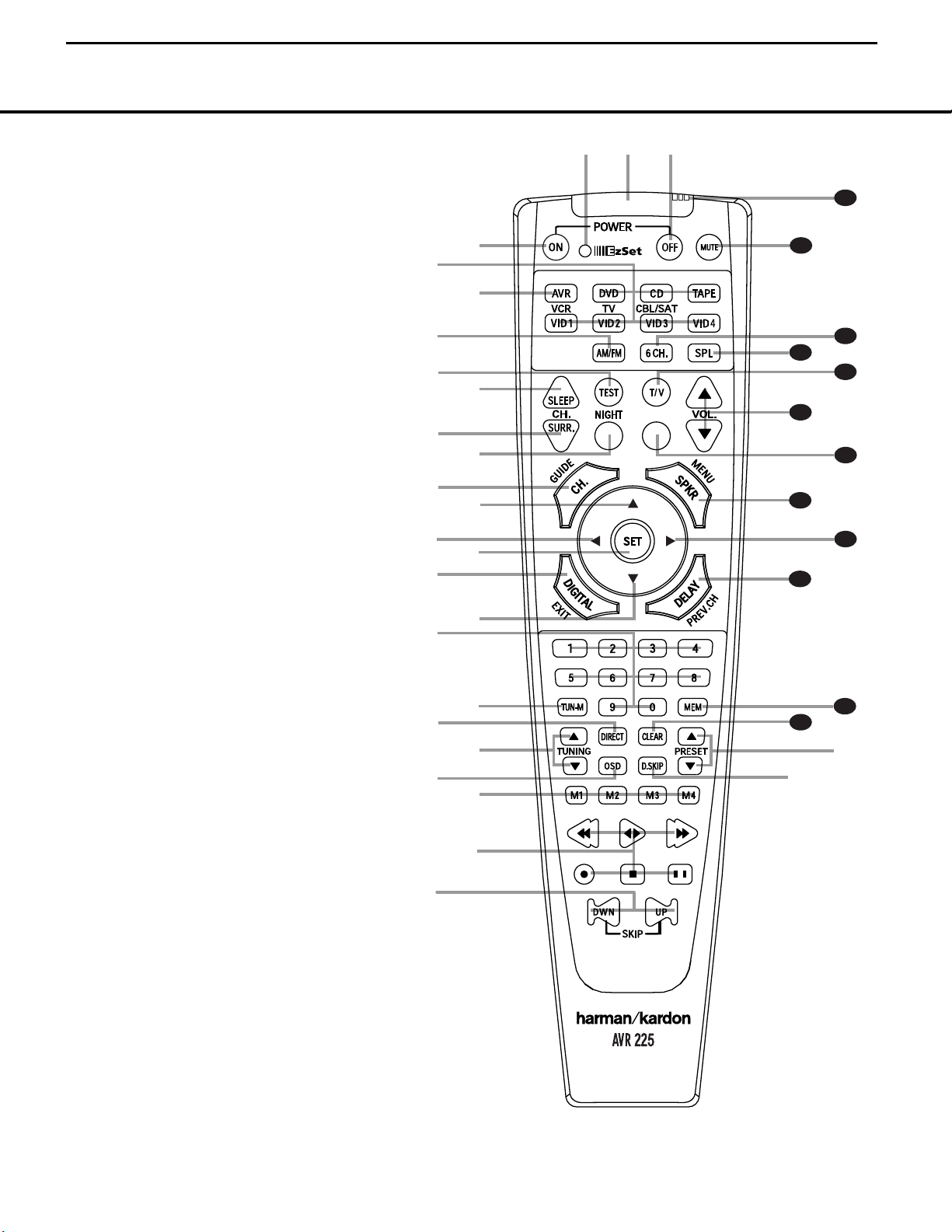
REMOTE CONTROL FUNCTIONS 11
●
●
●
●
●
●
●
●
●
●
●
●
REMOTE CONTROL FUNCTIONS
a
bc
d
e
f
g
h
i
j
k
l
m
n
p
o
q
s
r
t
u
v
w
`
32
30
29
28
37
36
35
34
33
31
38
z
x
y
39
a Power Off Button
b IR Transmitter Window
c Program/SPL Indicator
d Power On Button
e Input Selectors
f AVR Selector
g AM/FM Tuner Select
h Test Button
i Sleep Button
j Surround Mode Selector
k Night Mode
l Channel Select Button
m
⁄
Button
n
‹
Button
o Set Button
p Digital Select
q
¤
Button
r Numeric Keys
s Tuner Mode
t Direct Button
u Tuning Up/Down
v OSD Button
w Macro Buttons
x Transport Controls
y Skip Up/Down Buttons
z Disc Skip Button
` Preset Up/Down
28
Clear Button
29
Memory Button
30
Delay/Prev. Ch.
31
›
Button
32
Speaker Select
33
Spare Button
34
Volume Up/Down
35
TV/Video Selector
36
SPL Button
37
6-Channel Direct Input
38
Mute
39
EzSet Sensor Microphone
NOTE: The function names shown here are each
button’s feature when used with the AVR 225. Most
buttons have additional functions when used with
other devices. See pages 36–37 for a list of these
functions.
AVR225
11
harman/kardon
Page 12
12 REMOTE CONTROL FUNCTIONS
REMOTE CONTROL FUNCTIONS
IMPORTANT NOTE: The AVR 225’s remote may be
programmed to control up to eight devices, including
the AVR 225. Before using the remote, it is important
to remember to press the Input Selector Button e
that corresponds to the unit you wish to operate. In
addition, the AVR 225’s remote is shipped from
the factory to operate the AVR 225 and most
Harman Kardon CD or DVD players and cassette
decks.The remote is also capable of operating a wide
variety of other products using the control codes that
are part of the remote. Before using the remote with
other products, follow the instructions on page 32 to
program the proper codes for the products in your
system.
It is also important to remember that many of the buttons on the remote take on different functions, depending on the product selected using the device control
selectors.The descriptions shown here primarily detail
the functions of the remote when it is used to operate
the AVR 225. (See pages 36–37 for information about
alternate functions for the remote’s buttons.)
a Power Off Button: Pressing this button turns off
(places in the Standby mode) the device that was last
selected by pressing one of the Input Selectors e.
To place the AVR 225 in the Standby mode, first press
the AVR Selector Button f and then press this
button.
b IR Transmitter Window: Point this window toward
the AVR 225 when pressing buttons on the remote to
make certain that infrared commands are properly
received.
c Program/SPL Indicator: This three-color indica-
tor is used to guide you through the process of programming the remote and it is also used as a level
indicator when using the remote’s EzSet capabilities.
(See page 21 for more information on setting output
levels, and see page 32 for information on programming the remote.)
d Power On Button: Press this button to turn on
power to the device that was last selected by pressing
one of the Input Selectors e.To turn on the
AVR 225, press the AVR Selector Button f.
e Input Selectors: Pressing one of these buttons
will perform three actions at the same time. First, if the
AVR 225 is not turned on, this will power up the unit.
Next, it will select the source shown on the button as
the input to the AVR 225. Finally, it will change the
remote control so that it controls the device selected.
After pressing one of these buttons you must press
the AVR Selector Button f again to operate the
AVR 225’s functions with the remote.
f AVR Selector: Pressing this button will switch the
remote so that it will operate the AVR 225’s functions. If
the AVR 225 is in the Standby mode, it will also turn the
AVR 225 on.
g AM/FM Tuner Select: Press this button to select
the AVR 225’s tuner as the listening choice. Pressing
this button when the tuner is already in use will switch
between the AM and FM bands.
h Test Button: Press this button to begin the
sequence used to manually calibrate the AVR 225’s
output levels.To begin automatic calibration using the
EzSet feature, press the SPL Button instead
of this button. (See page 21 for more information on
calibrating the AVR 225.)
i Sleep Button: Press this button to place the unit
in the Sleep mode.After the time shown in the display,
the AVR 225 will automatically go into the Standby
mode. Each press of the button changes the time until
turn-off in the following order:
This button is also used to change channels on your
TV when the TV is selected, and to end the process of
creating a macro command. (See page 33 for more
information on creating macros.)
j Surround Mode Selector: Press this button to
begin the process of changing the surround mode.
After the button has been pressed, use the
⁄/¤
Buttons mq to select the desired surround
mode. (See page 25 for more information.) Note that
this button is also used to tune channels when the TV
is selected and during the process of erasing stored
macro commands. (See page 33 for more information
on macros.)
NOTE: The Sleep Button i and Surround Mode
Selector j may also function as the Channel +
and – keys when the remote is programmed for use
with TVs, cable boxes, VCRs, satellite receivers or other
video devices with tuners. See page 34 for information
on programming the remote for Channel Control
Punch-Through capability so that you may change
channels on a separate device when the remote is in
AVR mode.
k Night Mode: Press this button to activate
the Night mode.This mode is available in specially
encoded digital sources, and it preserves dialogue
(center channel) intelligibility at low volume levels.
l Channel Select Button: This button is used to
start the process of setting the AVR 225’s output levels to
an external source. Once this button is pressed, use the
⁄/¤
Buttons mq to select the channel being
adjusted, then press the Set Button o,followed by
the
⁄/¤
Buttons mq again, to change the level
setting. (See page 29 for more information.)
m
⁄
Button: This multipurpose button is used to
change or scroll through items in the on-screen menus,
or to change configuration settings such as output
levels.When changing an item such as the surround
mode or digital input directly, first press the function or
mode to be changed (e.g., press the Surround Mode
Selector j to select a surround mode or the Digital
Select Button p to change the digital input) and
then press this button to scroll through the list of available choices.
n
‹
Button: This button is used to change the
menu selection or setting during some of the setup
procedures for the AVR 225.
o Set Button: This button is used to enter settings
into the AVR 225’s memory. It is also used in the
setup procedures for delay time, speaker configuration
and channel output level adjustment.
p Digital Select: Press this button to assign one of
the digital inputs be#$ to a source. (See page
26 for more information on using digital inputs.)
q
¤
Button: This multipurpose button is used to
change or scroll through items in the on-screen menus,
or to change configuration settings such as output
levels.When changing an item such as the surround
mode or digital input directly, first press the function or
mode to be changed (e.g. press the Surround Mode
Selector j to select a surround mode or the Digital
Select Button p to change the digital input) and
then press this button to scroll through the list of available choices.
r Numeric Keys: These buttons serve as a 10-
button numeric keypad to enter tuner preset positions.
They are also used to select channel numbers when
TV has been selected on the remote, or to select track
numbers on a CD, DVD or LD player, depending on
how the remote has been programmed.
s Tuner Mode: Press this button when the tuner is
in use to select between automatic tuning and manual
tuning. In automatic tuning mode, the Auto Indicator
R will be lit, and only stations with acceptable signal
quality may be tuned by pressing the Tuning Up/
Down Buttons 8u. When the button is pressed
so that the Auto Indicator R goes out, manual tuning mode is engaged, and pressing the Tuning
Buttons 8u will move the frequency up or down
in single-step increments.When the FM band is in
use, pressing this button when a station’s signal is
90
min80min70min60min50min
40
min
30
min20min10min
OFF
AVR225
12
harman/kardon
36
Page 13

REMOTE CONTROL FUNCTIONS 13
weak will change to monaural reception. (See page
28 for more information.)
t Direct Button: When the tuner is in use, press
this button to start the sequence for direct entry of a
station’s frequency. After pressing the button simply
press the proper Numeric Keys r to select a station. (See page 28 for more information on the tuner.)
u Tuning Up/Down: When the tuner is in use, these
buttons will tune up or down through the selected frequency band. If the Tuner Mode Button s@ has
been pressed so that the Auto Indicator R is illuminated, pressing either of the buttons will cause the tuner
to seek the next station with acceptable signal strength
for quality reception. When the Auto Indicator R is
NOT illuminated, pressing these buttons will tune stations in single-step increments. (See page 28 for more
information.)
v OSD Button: Press this button to activate the On
Screen Display (OSD) system used to set up or adjust
the AVR 225’s parameters.
w Macro Buttons: Press these buttons to store or
recall a “Macro”, which is a preprogrammed sequence
of commands stored in the remote. (See page 33 for
more information on storing and recalling macros.)
x Transport Controls: These buttons do not have
any functions with the AVR 225 but they may be programmed for the forward/reverse play operation of a
wide variety of CD or DVD players, and audio or video
cassette recorders. (See page 34 for more information
on programming the Transport Control Punch-Through
capability of the remote.)
y Skip Up/Down Buttons: These buttons have no
direct function with the AVR 225, but when used with
a compatibly programmed CD or DVD changer they
will change the track or chapter of the disc currently
being played in the changer.
z Disc Skip Button: This button has no direct
function for the AVR 225, but when used with a compatibly programmed CD or DVD changer, it will change
the disc currently being played in the changer. (See
page 33 for more information on using the remote
with other devices.)
` Preset Up/Down: When the tuner is in use,
press these buttons to scroll through the stations
programmed into the AVR 225’s memory.When
some source devices, such as CD players,VCRs
and cassette decks, are selected using the device
Input Selectors e, these buttons may function
as Chapter Step or Track Advance.
Clear Button: Press this button to clear incorrect
entries when using the remote to directly enter a radio
station’s frequency.
Memory Button: Press this button to enter a
radio station into the AVR 225’s preset memory. Once
the Memory Indicator O flashes, you have five
seconds to enter a preset memory location using
the Numeric Keys r. (See page 28 for more
information.)
Delay/Prev Ch.: Press this button to begin
the process for setting the delay times used by the
AVR 225 when processing surround sound. After
pressing this button, the delay times are entered by
pressing the Set Button o and then using the
⁄/¤
Buttons mq to change the setting. Press
the Set Button o again to complete the process.
(See page 18 for more information.)
›
Button: Press this button to change a setting
or selection when configuring many of the AVR 225’s
settings.
Speaker Select: Press this button to begin the
process of configuring the AVR 225’s bass management system for use with the type of speakers used
in your system. Once the button has been pressed,
use the
⁄/¤
Buttons mq to select the chan-
nel you wish to set up. Press the Set Button o
and then select another channel to configure. When
all adjustments have been completed, press the
Set Button o twice to exit the settings and
return to normal operation. (See page 20 for more
information.)
Spare Button: This button does not have any
function for the operation of the AVR 225, but it is
available for use when programmed with the code
from another remote. (See page 32 for information
on programming the remote with codes for other
devices.)
Volume Up/Down: Press these buttons to raise
or lower the system volume. See page 34 for more
information on programming the Volume PunchThrough capability of the remote, which allows you to
change the AVR 225’s volume while the remote is set
to control another device.
TV/Video Selector: This button does not have a
direct function on the AVR 225, but when used with a
compatibly programmed VCR, DVD or satellite receiver
that has a “TV/Video” function, pressing this button will
switch between the output of the player or receiver
and the external video input to that player. Consult the
owner’s manual for your specific player or receiver for
the details of how it implements this function.
SPL Button: This button activates the AVR 225’s
EzSet function to quickly and accurately calibrate the
AVR 225’s output levels. Press and hold the button for
three seconds and then release it. The Test Tone will
begin circulating, and the Program/SPL Indicator c
will change colors. During this sequence, EzSet will
automatically adjust the output levels for all channels
until they have equal output levels, as shown by the
Program/SPL Indicator c lighting green for each
channel. (See page 21 for more information on EzSet.)
6-Channel Direct Input: Press this button to
select the component connected to the 6-Channel
Direct Inputs i as the source.
Mute: Press this button to momentarily silence
the AVR 225 or TV set being controlled, depending on
which device has been selected. When the AVR 225
is muted, press this button or use the Volume Control
Ó to return to the previous volume level.
When the AVR 225 remote is being programmed to
operate another device, or when a macro command is
being programmed, this button is pressed with the
Input Selector Button e to begin the programming process. (See page 33 for more information.)
Ez Set Sensor Microphone: The sensor micro-
phone for the EzSet microphone is behind these slots.
When using the remote to calibrate speaker output
levels using EzSet, be sure that you do not hold the
remote in a way that covers these slots. (See page 21
for more information on using EzSet.)
REMOTE CONTROL FUNCTIONS
AVR225
13
harman/kardon
28
29
30
31
32
36
37
38
34
39
33
34
35
Page 14
14 INSTALLATION AND CONNECTIONS
System Installation
After unpacking the unit, and placing it on a solid surface
capable of supporting its weight, you will need to make
the connections to your audio and video equipment.
Audio Equipment Connections
We recommend that you use high-quality interconnect
cables when making connections to source equipment
and recorders to preserve the integrity of the signals.
When making connections to audio source equipment
or speakers it is always a good practice to unplug the
unit from the AC wall outlet. This prevents any possibility of accidentally sending audio or transient signals
to the speakers that may damage them.
1. Connect the analog output of a CD player to the
CD Inputs £.
NOTE: When the CD player has both fixed and vari-
able audio outputs it is best to use the fixed output
unless you find that the input to the receiver is so low
that the sound is noisy, or so high that the signal is
distorted.
2. Connect the analog Play/Out jacks of a cassette
deck, MD, CD-R or other audio recorder to the Tap e
Input Jacks ∞. Connect the analog Record/In jacks
on the recorder to the Tape Output Jacks ¢ on the
AVR 225.
3. Connect the output of any digital sources to the
appropriate input connections on the AVR 225 rear
panel. The Optical and Coaxial Digital Inputs
be
#$ may be used with a Dolby Digital or
DTS source such as a DVD player, or the output
of a conventional CD or LD player’s PCM (S/P-DIF)
output.
4. Connect the Optical Digital Audio Output ‡ or the
Coaxial Digital Audio Output ° on the rear panel of
the AVR 225 to the matching digital input connections on
a CD-R or MiniDisc recorder.
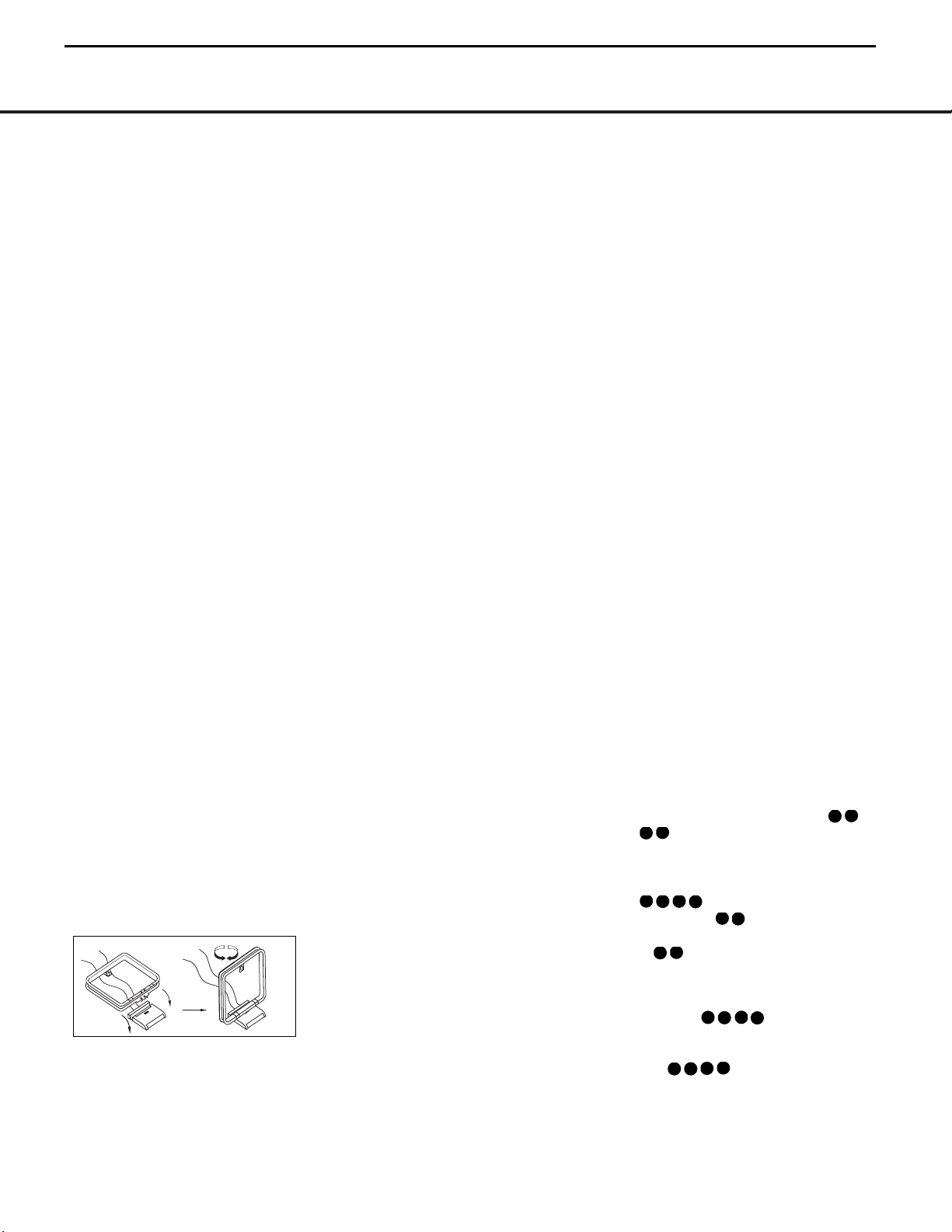
5. Assemble the AM Loop Antenna supplied with the
unit as shown below. Connect it to the AM and GND
Screw Terminals ¡.
6. Connect the supplied FM antenna to the FM
Antenna (75-Ohm) Connection ™. The FM anten-
na may be an external roof antenna, an inside powered or wire lead antenna or a connection from a
cable TV system. Note that if the antenna or connection uses 300-ohm twin-lead cable, you must use the
300-ohm-to-75-ohm adapter supplied with the unit to
make the connection.
7. If you have a DVD-Audio or SACD player, or other
component that includes an onboard surround
decoder and 6-channel line-level audio outputs, you
may connect these audio outputs to the 6-Channel
Direct Inputs i.
8. Connect the front, center and surround Speaker
Outputs ª‚⁄¤‹ to the respective speakers.
To ensure that all the audio signals are carried to your
speakers without loss of clarity or resolution, we suggest that you use high-quality speaker cable. Many
brands of cable are available and the choice of cable
may be influenced by the distance between your
speakers and the receiver, the type of speakers you
use, personal preferences and other factors.Your dealer
or installer is a valuable resource to consult in selecting the proper cable.
Regardless of the brand of cable selected, we
recommend that you use a cable constructed of fine,
multistrand copper with a gauge of 14 or smaller.
Remember that in specifying cable, the lower the
number, the thicker the cable.
Cable with a gauge of 16 may be used for short runs
of less than 10 feet. We do not recommend that you
use cables with an AWG equivalent of 18 or higher due
to the power loss and degradation in performance that
will occur.
Cables that are run inside walls should have the appropriate markings to indicate listing with UL, CSA or other
appropriate testing agency standards. Questions about
running cables inside walls should be referred to your
installer or a licensed electrical contractor who is familiar with the NEC and/or the applicable local building
codes in your area.
When connecting wires to the speakers, be certain to
observe proper polarity. Remember to connect the
“negative” or “black” wire to the same terminal on
both the receiver and the speaker. The AVR 225 conforms to the latest CEA-recommended color-coding
for speaker terminals. Accordingly, the positive (+)
terminal, which was previously red, is now a specific
color to assist you in making the correct connections.
If your speakers have color-coded connections, match
the terminal on the AVR 225 to the like terminal on
your speakers. For existing speakers with a red terminal for the positive connection, the connections on the
AVR 225 are as follows:
Front Left = White Front Right = Red
Center = Green
Surround Left = Blue Surround Right = Gray
NOTE: While most speaker manufacturers adhere to
an industry convention of using black terminals for
negative and red ones for positive, some manufacturers may vary from this configuration. To ensure proper
phase and optimal performance, consult the identification plate on your speaker or the speaker’s manual to
verify polarity. If you do not know the polarity of your
speaker, ask your dealer for advice before proceeding,
or consult the speaker’s manufacturer.
We also recommend that the length of cable used
to connect speaker pairs be identical. For example,
use the same length piece of cable to connect the
front-left and front-right or surround-left and surround-right speakers, even if the speakers are a
different distance from the AVR 225.
9. Connections to a subwoofer are normally made via
a line-level audio connection from the Subwoofer
Output • to the line-level input of a subwoofer with
a built-in amplifier. When a passive subwoofer is used,
the connection first goes to a power amplifier, which
will be connected to one or more subwoofer speakers.
If you are using a powered subwoofer that does not
have line-level input connections, follow the instructions furnished with the speaker for connection
information.
Video Equipment Connections
Video equipment is connected in the same manner as
audio components.Again, the use of high-quality interconnect cables is recommended to preserve signal
quality.
Although any compatible video device may be connected to any video input (with the exception of the
Video 1 and Video 2 Out Jacks dg
, which may only be connected to a video
recorder), to make programming device codes into
the remote control easier, we recommend that you
connect your VCR to the Video 1 Connectors cd
, your television to the Video 2 Input
Connectors f , and your cable-TV converter
or satellite receiver to the Video 3 Input Connectors
h .
1. Connect a VCR’s or other video source’s audio and
video Play/Out jacks to the Video 1 or Video 2 In
Jacks cf on the rear panel. The
Audio and
Video Record/In jacks on the VCR should be
connected
to the Video 1 or Video 2 Out Jacks
dg on the AVR 225.
INSTALLATION AND CONNECTIONS
AVR225
14
harman/kardon
35
39
38
34
32
34
33
35
36
37
41
40
32
36
33
38
35
34
37
39
Page 15

INSTALLATION AND CONNECTIONS 15
INSTALLATION AND CONNECTIONS
2. Connect the analog audio and video outputs of a
television set or any other video source to the Video 2
Input Jacks f .
3. Connect the analog audio and video outputs of a
cable TV converter or satellite receiver, or any other
video source, to the Video 3 Jacks h .
4. Connect the analog audio and video outputs of
a DVD or laser disc player to the DVD Jacks a
k . When a digital audio connection is used
for your DVD player, the default connection is the
Coaxial Digital Audio Input 1 Jack b.However,
the connection may also be made to any of the
Optical e # or Coaxial b $ digital audio
inputs, provided that the digital input source selection
is changed as shown on pages 17 and 26. If your
DVD or DVD-Audio player includes an onboard surround decoder and 6-channel line-level audio outputs, you may connect these audio outputs to the
6-Channel Direct Inputs i. When you wish to
hear this decoded audio, select the DVD input first in
order to select the video signal from the DVD player,
then select the 6-Channel Direct Input source for the
audio.
5. Connect the digital audio outputs of a DVD player,
satellite receiver, cable box or HDTV converter to the
appropriate Optical or Coaxial Digital Audio Inputs
be
#$.
6. Connect the Video Monitor Output ·j jacks
on the receiver to the composite or S-Video input of
your television monitor or video projector.
VIDEO CONNECTION NOTE:
• Composite and S-Video signals may only be viewed
in their native formats. The AVR 225 will not convert
signals from composite to S-Video, or vice versa.
S-Video inputs may only be viewed when the
AVR 225 is connected to a TV set or video display
with S-Video capability. If you use both standard
composite video and S-Video sources in your
system, it is important that you connect both an
S-Video cable and a standard composite video
cable (a coax cable with an RCA plug on both ends)
between the AVR 225 and your TV or projector.
When it is necessary to make both types of
connections to your TV set, use different inputs if
possible. Consult the instructions for your TV set or
projector for more information on connecting both
types of signals.
Power Connections
This unit is equipped with two accessory AC outlets.
They may be used to power accessory devices, but
they should not be used with high-current draw equipment such as power amplifiers.The total power draw
to each outlet may not exceed 100 watts.
The Switched AC Accessory Outlet › will receive
power only when the unit is on. This is recommended
for devices that have no power switch or a mechanical
power switch that may be left in the “ON” position.
NOTE: Many audio and video products go into a
Standby mode when they are used with switched outlets, and cannot be fully turned on using the outlet
alone without a remote control command.
The Unswitched AC Accessory Outlet fi will
receive power as long as the unit is plugged into a
powered AC outlet.
Finally, when all connections are complete, plug the
Power Cord fl into a nonswitched 120-volt AC wall
outlet. You’re almost ready to enjoy the AVR 225!
AVR225
15
harman/kardon
37
31
36
40
41
Page 16

SYMPTOM CAUSE SOLUTION
Unit does not function when Main • No AC Power • Make certain AC power cord is plugged into a live outlet
Power Switch is pushed • Check to see whether outlet is switch-controlled
Display lights, but no sound • Intermittent input connections • Make certain that all input and speaker connections are secure
or picture • Mute is on • Press Mute button
• Volume control is down • Turn up volume control
Unit turns on, but front-panel • Display brightness is turned off • Follow the instructions in the Display Brightness section
display does not light up on page 30 so that the display is set to VFD FULL
No sound from any speaker; • Amplifier is in protection mode • Check speaker wire connections for shorts at receiver and
light around power switch is red due to possible short speaker ends
• Amplifier is in protection mode • Contact your local Harman Kardon service center, which you can
due to internal problems locate by visiting our Web site at www.harmankardon.com
No sound from surround or • Incorrect surround mode • Select a mode other than Stereo or Dolby 3 Stereo
center speakers • Input is monaural • There is no surround information from mono sources
• Incorrect configuration • Check speaker mode configuration
• Stereo or Mono program material • The surround decoder may not create center- or rear-channel
information from nonencoded programs
Unit does not respond to • Weak batteries in remote • Change remote batteries
remote commands • Wrong device selected • Press the AVR selector
• Remote sensor is obscured • Make certain front-panel sensor is visible to remote
or connect remote sensor
Intermittent buzzing in tuner • Local interference • Move unit or antenna away from computers, fluorescent
lights, motors or other electrical appliances
Letters flash in the channel indicator • Digital audio feed paused • Resume play for DVD
display and digital audio stops • Check that Digital Input is selected
Processor Reset
In the rare case in which the unit’s operation or displays
seem abnormal, the cause may involve the erratic
operation of the system’s memory or microprocessor.
To correct this problem, first unplug the unit from the
AC wall outlet and wait at least three minutes. After the
pause, reconnect the AC power cord and check the
unit’s operation. If the system still malfunctions, a system “reset” may clear the problem.
To clear the AVR 225’s entire system memory including tuner presets, output level settings, delay times and
speaker configuration data, first put the unit in Standby
by pressing the System Power Control Button 2.
Next, press and hold the Tone Mode Button 6 for
three seconds.
The unit will turn on automatically and display the
RESET message in the Main Information
Display S. Note that once you have cleared the
memory in this manner, it is necessary to reestablish all
system configuration settings and tuner presets.
The reset will not affect settings that were programmed into the remote control. To reset the remote
control and restore it to its factory default settings,
please follow the instructions on page 34.
If these steps do not solve the problem, consult an
authorized Harman Kardon service center.You can
locate the service center nearest to you by visiting our
Web site at www.harmankardon.com.
Memory Backup
This product is equipped with a memory backup
system that preserves the system configuration information and tuner presets if the unit is accidentally
unplugged or subjected to a power outage.This memory will last for approximately one week, after which
time all information must be reentered.
TROUBLESHOOTING GUIDE
Your AVR 225 receiver has been designed to provide many years of trouble-free service. In the event that you are experiencing difficulties, please check the suggestions
below for a possible solution to your problem. Additional information on the AVR 225, including updated information and user hints, is available from our Web site at
www.harmankardon.com.
AVR225
16
harman/kardon
16 TROUBLESHOOTING GUIDE
Page 17
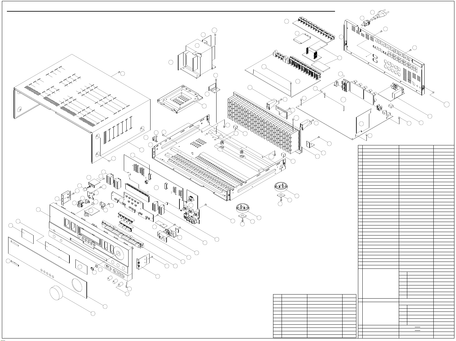
AVR225
17
5
4
S9
x4
39-4
31
39-3
S1
F.I.P (DISPLAY)
# HFLCM2054C
6
x7
S5
S5
39-6
x2
22
21
20
x6
S7
18
S2
x2
37-5
14
S2
x3
8
13
12
7
37-4
37-6
S3
S2
37-2
S2
15
37-1
37-3
43
37-8
11
10
S2
9
5
41
40
S1
x6
3
x3
8
2
1
S5
39-8
29
19
S2
x7
16
harman/kardon
39-2
42
33
35
34
S1
S8
x27
41
x2
S11
32
39-1
30
S5
x2
S4
x2
S12
S5
x2
28
25
S10
x5
25
23
S4
x2
S2
x12
24
23
S4
x2
DESCRIPTION
NO
SCREW
S1
SCREW
S2
SCREW
S3
SCREW
S4
SCREW
S5
SCREW
S6
SCREW
S7
SCREW
S8
SCREW,TRANS
S9
SCREW CTB3+6J 7
S10
SCREW,SPECIAL CHD1A012Z 2
S11
SCREW,SPECIAL CHD2A012 4
S12
S6
x2
S4
x3
S5
x2
38
S10
x2
40
17
37-7
S4
S4
S5
x2
27
26
24
PARTS NO.
CTB3+8JFZ
CTB3+10G
CTWS3+10G
CTW3+8J
CTB3+8J
CTW3+12J
CTB4+6FFZ
CTB3+10GFZ
CHD1A023
DESCRIPTION
NO
KNOB,VOLUME CBN1A155K128 1
1
WINDOW,FIP CGU1A280W 1
2
KNOB,ROTARY CBN1A156K128 3
3
BDAGE,HARMAN/KARDON KGB1A111Z 1
4
5
SHEET KMZ1A077 2
SHEET,FIP KMZ1A76 1
6
PANEL,FRONT CGW1A337R4XK128 1
7
BRACKET,SIDE CMD1A443 2
8
KNOB,FUNCTION CBT1A816M7G2 1
9
KNOB,SET CBT1A818YK128 1
10
KNOB,DELAY CBT1A819M7G2 1
11
KNOB,POWER CBT1A817K128 1
12
INDICATOR,POWER CGL1A200 1
13
KNOB,MOMS CBC1A139YK128 1
14
BRACKET,PCB CMK1A010 1
15
PLATE,SHIELD CMC1A180 1
16
CUSHION,RUBBER 1CHG1A157
17
HOLDER,LED A CMH1A167 2
18
HOLDER,LED B CMH1A168 2
19
BRACKET,FLT CMD1A374 2
20
CABINET,TOP CKC1B128S1 1
21
CHASSIS,BOTTOM CUA1A213 1
22
RUBBER,CUSHION KHG1A050 4
23
FOOT CKL1A069H43 4
24
SUPPORT,CUSHION CHG1A233 2
25
HEAT SINK CMY1A193 1
26
BRACKET,PCB KMD1A417 2
27
HOLDER,PCB KHE1A170 2
28
BRACKET,TRANS CMD1A464 1
29
BRACKET,PCB(H/T) KMD1A416 2
30
TRANS,POWER 1
31
BRACKET,PCB CMD1A387 2
32
PANEL,REAR CKF1A235Y 1
33
BUSHING,AC CORD KHR1A028 1
34
CORD,POWER CJA523FBY 1
35
36
FRONT PCB ASS'Y
37
Q,ty
14
MAIN PCB ASS'Y
38
28
INPUT PCB ASS'Y
39
1
8
12
2
6
27
4
NUT
40
WASHER
41
PLATE,SHIELD
42
PLATE,SHIELD A
43
PARTS NO. Q,ty
KMZ176
CLT5W006ZU
COP11516E
37-1
FIP PCB
37-2
KEY PCB
37-3
TONE PCB
37-4
PHONE PCB
37-5
MOMS PCB
37-6
POWER LED PCB
37-7
CONNECTOR PCB
37-8
DIGITAL INPUT
COP11517E
COP11518E 1
39-1
INPUT PCB
39-2
VIDEO PCB
39-3
TRANS PCB
39-4
TRANS PCB
39-6
TR PCB
39-8
BRIDGE DIODE
CMC1A188
CMC1A189 1
1
1
1
1
1
1
1
1
1
1
1
1
1
1
1
1
1
1
1
Page 18

AVR225
18
harman/kardon
AVR125/225 DISASSEMBLY PROCEDURE
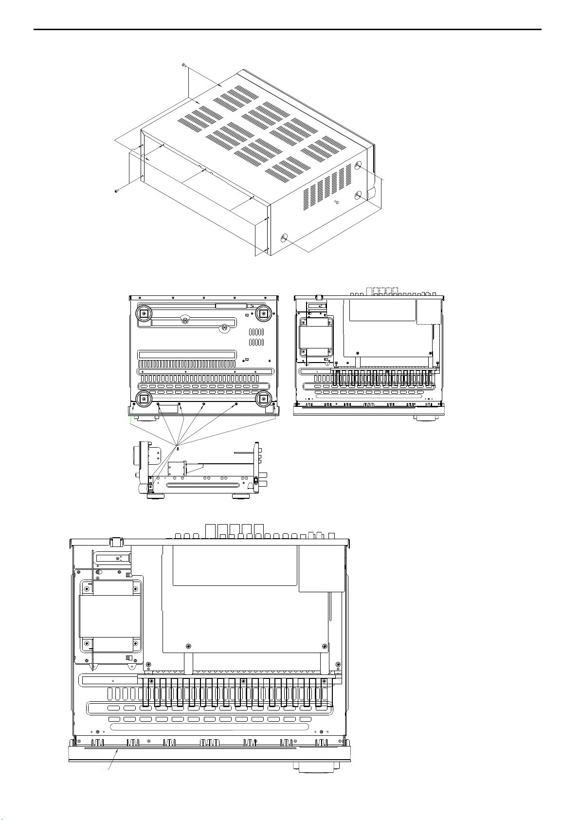
<1> TOP-CABINET(21) REMOVAL
1. Remove 13 screws(S1,S7) and then remove the Top-cabinet.
<2> FRONT PANEL ASS’Y REMOVAL
1. Remove the Top-cabinet, referring to the previous step<1>.
2. Disconnect the connect (BN72-Card canle)) on the FP PCB(37-1) from connector(CN72) on the Input PCB(39-1)
3. Disconnect the lead wire(BN80-8P) on the FP PCB(37-1) from connector(CN80) on the Main PCB(38).
4.Disconnect the lead wire(BN16-8P,BN10-4P) on the Tone PCB(37-3) from connector(CN16,CN10) on the Connect
PCB(37-7).
5. Disconnect the lead wire(BN41-6P) on the Tone PCB(37-3) from connector(CN41) on the Video PCB(39-2).
6. Disconnect the lead wire(BN18-5P) on the Digital input PCB(37-8) from connector(CN18) on the Input PCB(39-1).
7. Disconnect the lead wire(BN81-6P,BN83-2P) on the FP PCB(37-1) from connector(CN81.CN83) on the
Trans PCB(39-3).
8. Disconnect the lead wire(BN88-2P) on the Main PCB(38) from connector(CN88) on the Moms PCB(37-5).
9. Remove 1 screw(S10) and then lead wire(JW82-2P) on the Phone PCB(37-4).
10. Remove 9 screws(S1) and then remove the Front Panel ASS’Y.
<3> TONE PCB(37-3) REMOVAL
1. Rem ove the Top-cabinet , ref erring t o t he previous s tep< 1>.
2. Remove the Front Panel ASS’Y, referring to the previous step<2>.
3. Pull out the Volume Knob ASS’Y & 3 Rotary Knobs(5).
4. Remove 1 Nut(40), 1 Washer(41)
5. Remove 7 screws(S2) and then remove the Tone PCB(37-3).
6. Disconnect the lead wire(BN84-5P,BN90-2P) One the Tone PCB(37-3) from conne cto r (CN84,CN 90) on the
FP PCB(37-1)
7. Disconnect the lead wire (BN87-6P) One the Tone PCB(37-3) from connector(CN87) on the Phone PCB(37-4)
<4>PHONE PCB(37-4) REMOVAL
1. Rem ove the Top-cabinet , ref erring t o t he previous s tep< 1>.
2. Remove the Front Panel ASS’Y, referring to the previous step<2>.
3. Disconnect the lead wire (BN87-6P) One the Tone PCB(37-3) from connector(CN87) on the Phone PCB(37-4)
4. Remove 2 screws(S2,S3) and then remove the Phone PCB(37-4)
.
<5>POWER LED PCB(37-6) REMOVAL
1. Rem ove the Top-cabinet , ref erring t o t he previous s tep< 1>.
2. Remove the Front Panel ASS’Y, referring to the previous step<2>.
3. Remove 2 screws(S2) and then remove the Power led PCB(37-6).
4. Disconnect the lead wire(BN88-4P) from connector(CN88) on the FP PCB(37-1).
<6>FRONT PCB(37-1) REMOVAL
1. Rem ove the Top-cabinet , ref erring t o t he previous s tep< 1>.
2. Remove the Front Panel ASS’Y, referring to the previous step<2>.
3. Remove the Tone PCB(37-3), referring to the previous step<3>.
4. Remove the Phone PCB(37-4), referring to the previous step<4>.
5. Remove the Power led PCB(37-6), referring to the previous step<5>.
6. Remove 6 screws(S2) and then remove the Front PCB(37-1)
Page 19

AVR225
19
<7>TUNER MODULE(40) REMOVAL
1. Rem ove the Top-cabinet , ref erring t o t he previous s tep< 1>.
2. Disconnect the connector(CON1-Card cable) from connector(CN13) on the Input PCB ASS’ Y(39-1) .
3. Remove 2 screws(S8) and then remove the Tuner Module(40).
<8>VIDEO PCB(39-2) REMOVAL
1. Remove the Top-cabinet, referring to the previous step<1>.
2. Disconnect the lead wire(BN41-6P) on the Tone PCB(37-3) from connector(CN41) on the Video PCB(39-2).
3.Disconnect the connector (CN15-Card cable) on the Input PCB(39-1) from lead wire(CN43) on the Video PCB(39-2).
4. Remove 6 screws(S8) and then remove the Video PCB(39-2).
<9>INPUT PCB(39-1) REMOVAL
1. Rem ove the Top-cabinet , ref erring t o t he previous s tep< 1>.
2. Remove the Connect PCB(37-7).
3. Disconnect the lead wire(BN18-5P) on the Digital input PCB(37-8) from connector(CN18) on the Input PCB(39-1).
4. Disconnect the connect (BN72-Card canle)) on the FP PCB(37-1) from connector(CN72) on the Input PCB(39-1)
5. Remove 13 screws(S8,S11) and then remove the Input PCB(39-1).
<10>POWER TRANS(31) REMOVAL
1. Remove the Top-cabinet, referring to the previous step<1>.
2. Disconnect the connector (CN20,BN96) on the Trans PCB from lead wire(CN20-3P,BN96-6P) on the
Main PCB( 3 8) .
3. Remove 1 screw(S5) and then remove the Tr PCB(39-6)
4. Remove 1 screw(S5) and then remove the Bridge Diode PCB(39-8)
3. Remove 4 Trans screws(S9) and then remove the Power Trans(31).
<11>MAIN PCB ASS’Y(38) REMOVAL
1. Remove the Top-cabinet, referring to the previous step<1>.
2. Remov e the Tuner module, refer r ing to the previous step<7>.
3. R emove the Video PCB, r eferri ng to the previo us step<8>.
4. Remove the Input PCB, referring to the previous step<9>.
5. Disconnect the lead wire(BN80-8P) on the FP PCB(37-1) from connector(CN80) on the Main PCB(38).
6. Disconnect the lead wire(BN88-2P) on the Main PCB(38) from connector(CN88) on the Moms PCB(37-5).
7. Disconnect the connector (CN20,BN96) on the Trans PCB from lead wire(CN20-3P,BN96-6P)
on the Main PCB(38)..
8. Remove 11screws(S1-1EA, S4-2EA, S6-2EA, S8-6EA) and then remove the Main PCB ASS’Y(38).
harman/kardon
Page 20
AVR225
20
DISASSEMBLY
1) REMOVAL OF TOP COVER
2) REMOVAL OF FRONT PANEL
harman/kardon
3) PRINCIPAL PARTS LOACTION
TRANS FORMER
FRONT PCB
TUNER
MODULE
INPUT PCB
MAIN PCB
Page 21
AVR225
21
AMPLIFIER SECTION BIAS ADJUSTMENT
Measurement condition
. No input signal or volume position is minimum.
Standard value.
. Ideal current = 48mA ( ± 5%)
. Ideal DC Voltage = 21.12mV ( ± 5%)
CUP11517X (MAIN PCB)
harman/kardon
CN63
CN62
VR62
VR64
CN64
VR61
CN61
VR63
DC VOLTMETER..............Connect to CN61, CN62, CN63, CN64, CN65
NO. Channel Adjust for
1 Front Left 21.12mV (±5%)
2 Front Right 21.12mV (±5%)
3 Center
4 Surround Left
5 Surround Right
21.12mV (±5%)
21.12mV (±5%)
21.12mV (±5%)
CN65
VR65
Adjustment
VR61
VR62
VR63
VR64
VR65
Page 22
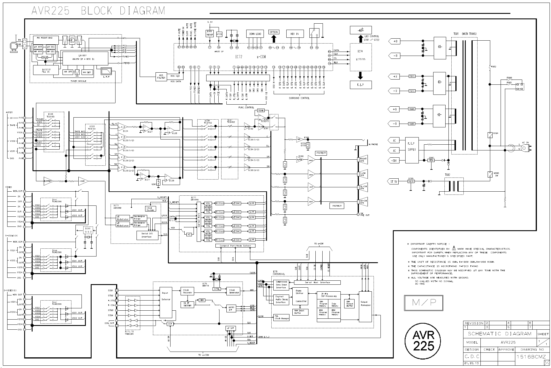
AVR225
22
harman/kardon
Page 23
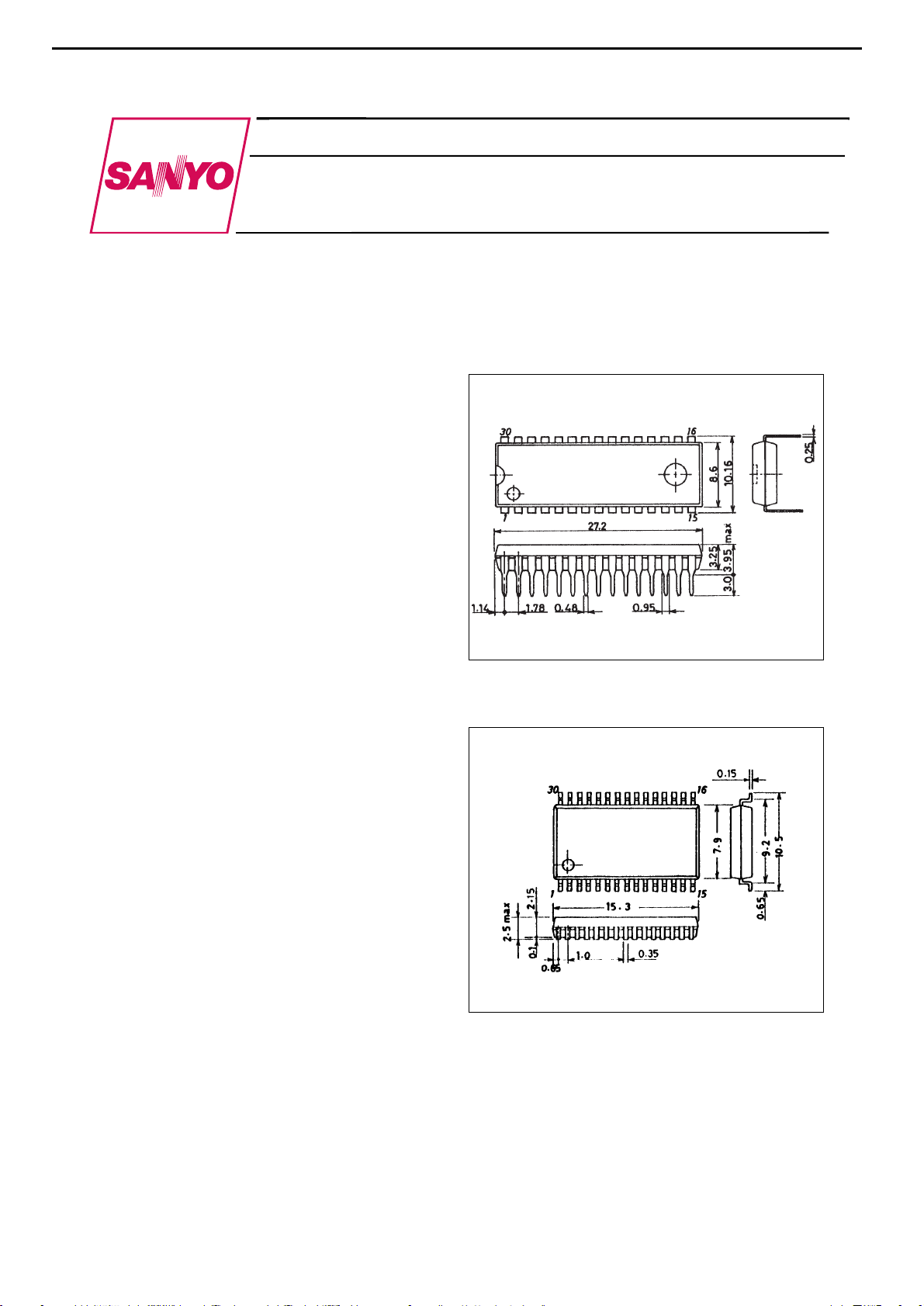
Overview
The LC74763 and LC74763M are on-screen display
CMOS LSIs that superimpose text and low-level
graphics onto a TV screen (video signal) under the
control of a microcontroller. The display characters
have a 12 by 18 dots structure, and 128 characters are
provided.
Features
• Display structure: 12 lines by 24 characters (up to 288
characters)
• Maximum character display: Up to 288 characters
• Character configuration: 12 (W) by 18 (H) dots
structure
• Number of characters: 128 characters (128 plus space
2 fonts)
• Character sizes: Three sizes (normal, double, and
triple sizes)
• Display starting positions: 64 horizontal and 64
vertical locations
• Reverse video function: Characters can be inverted on
a per character basis.
• Flashing types: Two types with periods of 0.5 and 1.0
second on a per character basis (duty fixed at 50%)
• Background color: One of eight colors (when internal
synchronization used)
• External control input: Serial data input in 8-bit units
• Built-in horizontal/vertical sync separation circuit,
AFC circuit, and synchronization detector
• Video output: Composite video signal output in
NTSC, PAL, PAL-M, PAL-N, PAL60, NTSC4.43, or
SECAM format
Package Dimensions
unit: mm
3196-DIP30SD
unit: mm
3216A-MFP30S
Preliminary
[LC74763M]
SANYO: MFP30S
[LC74763]
SANYO: DIP30SD
CMOS IC
LC74763, 74763M
On-Screen Display LSI
AVR225
23
LC74763M : IC53
harman/kardon
Page 24
Pin Functions
Pin No. Symbol Function Description
1 V
SS
Ground Ground connection
2 Xtal
IN1
Crystal oscillator connection
Connection for the crystal and capacitor used to form the crystal oscillator that generates
3 Xtal
OUT1
the internal synchronization signal. The oscillator can be selected with a command switch.
4 HSYNC
OUT
Horizontal synchronization Outputs the horizontal synchronization signal (AFC). The output polarity can be selected
output (metal option). Also functions as general output port (command switch).
5 Xtal
IN2
Crystal oscillator connection
Connection for the crystal and capacitor used to form the crystal oscillator that generates
6 Xtal
OUT2
the internal synchronization signal.
7 VSYNC
OUT
Vertical synchronization output
Outputs the vertical synchronization signal. The output polarity can be selected (metal
option). Also functions as general output port (command switch).
8 CS Enable input
Enables/disables serial data input. Serial data is enabled when this pin is low (hysteresis
input). Pull-up resistor built in (metal option).
9 SIN Data input Serial data input (hysteresis input). Pull-up resistor built in (metal option).
10 SCLK Clock input Clock input for serial data input (hysteresis input). Pull-up resistor built in (metal option).
SECAM mode switch input/
During input, switches between SECAM and other modes.
11 SECAM
output (command switch)
During output, functions as general output port or internal V output (command switch).
Low = other modes, high = SECAM mode
525/625 switch input/output
During input, switches between 525 scan lines and 625 scan lines.
12 525/625
(command switch)
During output, functions as general output port or character data output (command switch).
Low = 525 lines, high = 625 lines
NTSC/PAL switch input/output
Switches the color mode between NTSC and PAL.
13 NTSC/PAL
(command switch)
During output, functions as general output port or frame data output (command switch).
Low = NTSC, high = PAL
Switch FSC between 3.58 MHz and 4.43 MHz.
14 3.58/4.43 3.58/4.43 switch input/output During output, functions as general output port or halftone output (command switch).
(command switch) Low = 3.58, high = 4.43
15 RST Reset input
System reset input pin, low is active (hysteresis input).
Pull-up resistor built in (metal option).
16 CV
OUT
Video signal output Composite video output
17 V
DD2
Power supply connection Power supply connection for composite video signal level generation
18 CV
IN
Video signal input Composite video input
19 CV
CR
Video signal input SECAM chroma signal input
20 SYNC
IN
Sync separator circuit input Built-in sync separator circuit video signal input
21 SEP
C
Sync separator circuit Built-in sync separator circuit
22 V
SS
Ground Ground connection
23 PD
OUT
Control voltage output AFC control voltage output
24 AMP
IN
AFC filter connection Filter connection
25 AMP
OUT
26 FC Control voltage input AFC control voltage input
27 VCO
IN
LC oscillator connection VCO LC oscillator circuit coil and capacitor connection
28 VCO
OUT
External synchronization signal
Outputs the exclusive NOR of the horizontal synchronization signal (AFC) and CSYNC (sync
29 SYNC
DET
detection output
separator). The output polarity can be selected (metal option). Also functions as general
output port (command switch).
30 V
DD1
Power supply connection Power supply connection (+5 V: digital system power supply)
LC74763, 74763M
AVR225
24
harman/kardon
Page 25
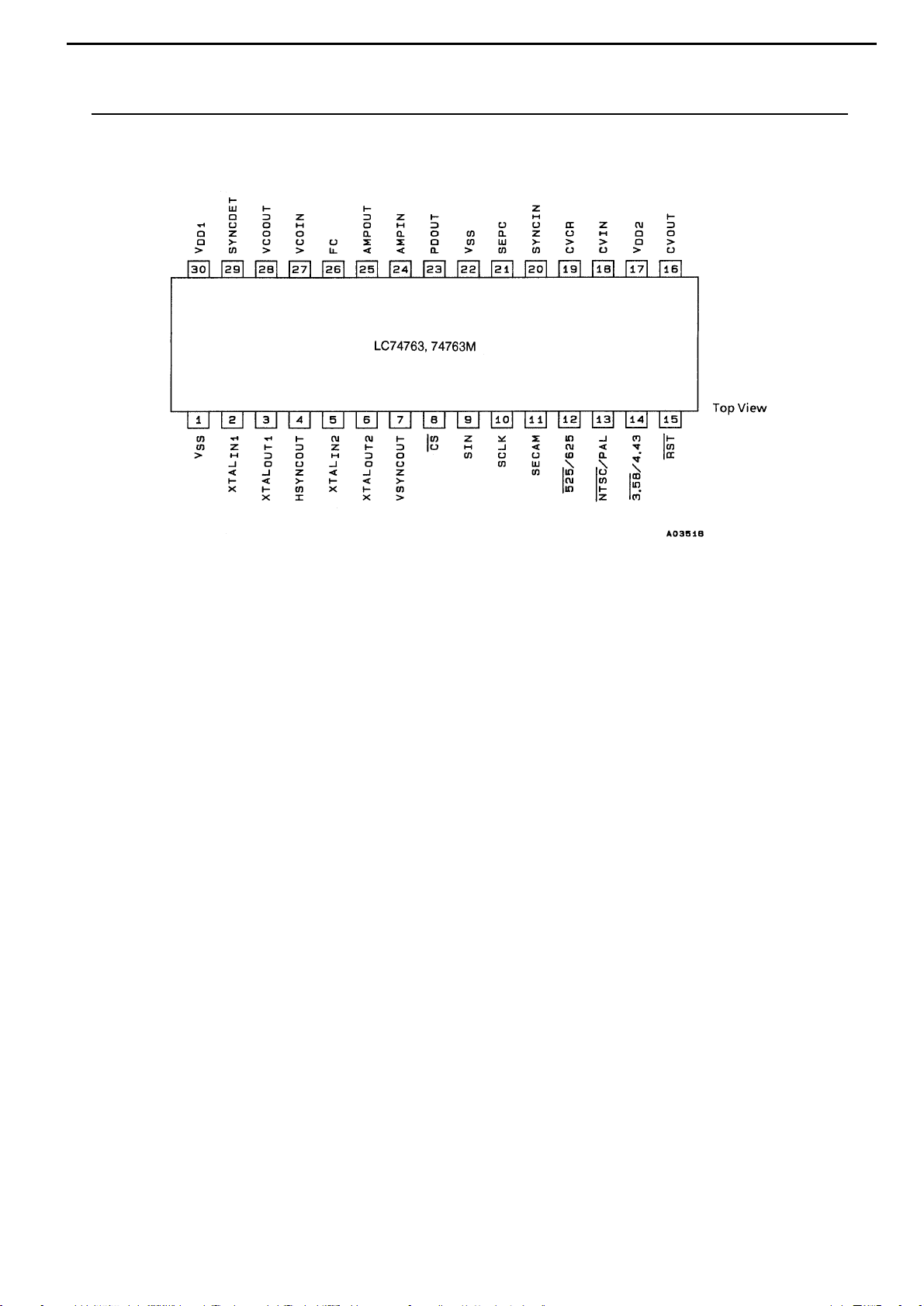
LC74763, 74763M
Pin Assignment
No. 5039-4/19
Top view
AVR225
25
harman/kardon
Page 26
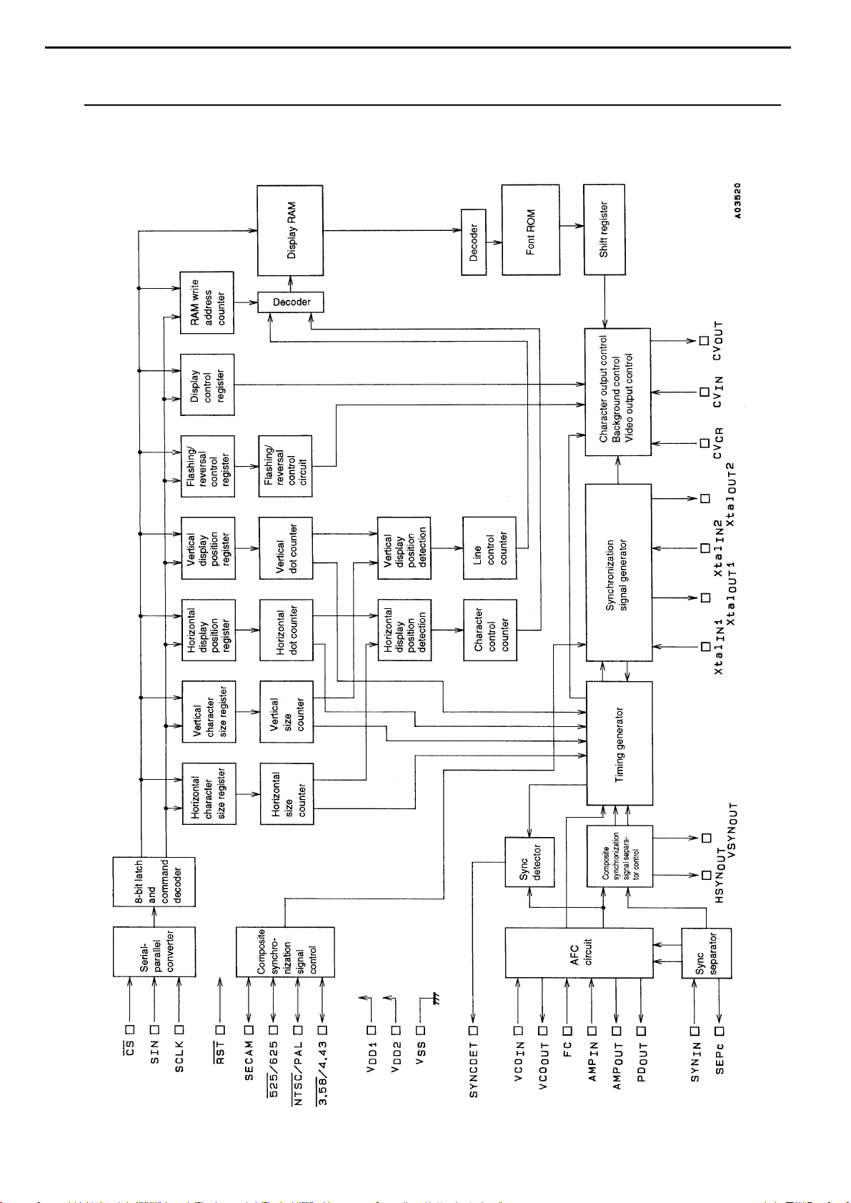
System Block Diagram
LC74763, 74763M
AVR225
26
harman/kardon
Page 27
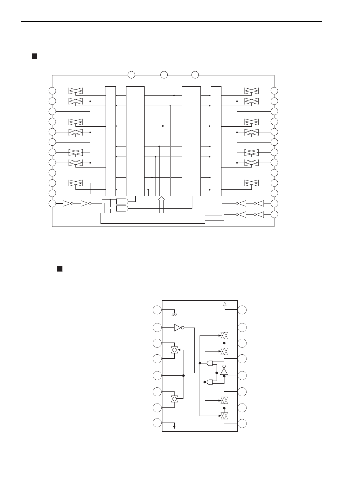
LEVEL SHIFTER
2
1
2
1
3
4
2
5
6
3
7
4
1
2
1
3
4
2
5
6
3
7
4
1
3
4
5
6
7
8
9
10
14 28
11
12
13
27
26
25
24
23
22
21
20
19
18
17
16
15
LATCH CIRCUIT
SHIFT REGISTER
LEVEL SHIFTER
LATCH CIRCUIT
L-S R-S
Vss GND VDD
L-S
L-COM
L-S
L-S
L-COM
L-S
L-S
L-COM
L-S
L-COM
ST
R-S
R-COM
R-S
R-S
R-COM
R-S
R-S
R-COM
R-S
R-COM
DATA
CK
LEVEL SHIFTER
2
1
2
1
3
4
2
5
6
3
7
4
1
2
1
3
4
2
5
6
3
7
4
1
3
4
5
6
7
8
9
10
14 28
11
12
13
27
26
25
24
23
22
21
20
19
18
17
16
15
LATCH CIRCUIT
SHIFT REGISTER
LEVEL SHIFTER
LATCH CIRCUIT
L-S R-S
Vss GND VDD
L-S
L-COM
L-S
L-S
L-COM
L-S
L-S
L-COM
L-S
L-COM
ST
R-S
R-COM
R-S
R-S
R-COM
R-S
R-S
R-COM
R-S
R-COM
DATA
CK
TC9162AF (FUNCTION/INPUT : IC30)
BLOCK DIAGRAM
TC9162AF (FUNCTION/INPUT : IC30)
BLOCK DIAGRAM
TC9215AF (TONE CONTROL : IC80)
BLOCK DIAGRAM
AVR225
27
harman/kardon
GND 1
OFF 2
3S
10
S
4
11
S
5
12
TC9215AF
16 V
15
S
S
14
S
13
S
12
DD
40
41
42
34
S
S
V
20
21
ss
6
7
8
11
10
9
S
S
S
32
31
30
Page 28
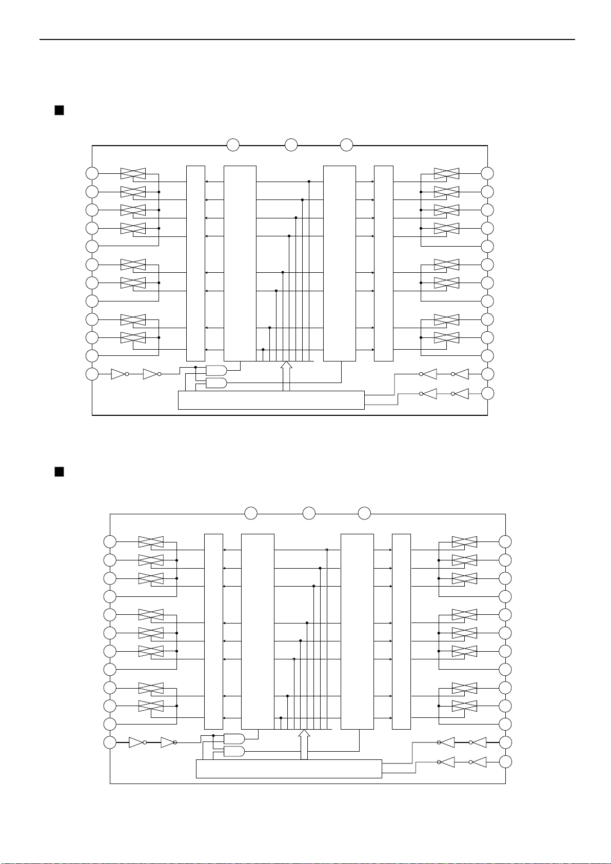
LEVEL SHIFTER
2
1
2
3
4
1
5
6
2
7
8
3
1
2
3
4
1
5
6
2
7
8
3
1
3
4
5
6
7
8
9
10
14 28
11
12
13
27
26
25
24
23
22
21
20
19
18
17
16
15
LATCH CIRCUIT
SHIFT REGISTER
LEVEL SHIFTER
LATCH CIRCUIT
L-S R-S
Vss GND VDD
L-S
L-S
L-S
L-COM
L-S
L-S
L-COM
L-S
L-S
L-COM
ST
R-S
R-S
R-S
R-COM
R-S
R-S
R-COM
R-S
R-S
R-COM
DATA
CK
LEVEL SHIFTER
2
1
2
3
1
4
5
6
2
7
8
3
1
2
3
1
4
5
6
2
7
8
3
1
3
4
5
6
7
8
9
10
14 28
11
12
13
27
26
25
24
23
22
21
20
19
18
17
16
15
LATCH CIRCUIT
SHIFT REGISTER
LEVEL SHIFTER
LATCH CIRCUIT
L-S R-S
Vss GND VDD
L-S
L-S
L-COM
L-S
L-S
L-S
L-COM
L-S
L-S
L-COM
ST
R-S
R-S
R-COM
R-S
R-S
R-S
R-COM
R-S
R-S
R-COM
DATA
CK
TC9164AF (FUNCTION/INPUT) : IC22
BLOCK DIAGRAM
TC9163AF (FUNCTION/INPUT) : IC20
BLOCK DIAGRAM
AVR225
28
harman/kardon
Page 29

AVR225
29
TC9482F (ELECTRONIC VOLUME/INPUT) : IC31
NC VSS VDD TEST
2
1
28 27
harman/kardon
L-OUTA
L-INA
L-A-GNDA
L-OUTB
L-INB
L-A-GNDB
L-OUTC
L-INC
L-A-GNDC
CS1
GND
10
11
12
13
3
4
5
6
7
8
9
1dB
VR
latch
8dB
VR
latch
1dB
VR
latch
8dB
VR
latch
1dB
VR
latch
8dB
VR
latch
Shift register (32BIT)
Level shift circuit
3 to 7
decoder
4 to 13
decoder
Same as L-ch
Circuit
Strobe generate
circuit
3
4
5
6
7
8
9
10
11
12
13
L-OUTA
L-INA
L-A-GNDA
L-OUTB
L-INB
L-A-GNDB
L-OUTC
L-INC
L-A-GNDC
CS1
GND
CK
14
14
CK
Page 30

AVR225
harman/kardon
30
Page 31

AVR225
harman/kardon
31
Page 32

AVR225
32
harman/kardon
Page 33

PIN No. Pin Name I/O Function
1,12,23 +VD1 - Digital Power supply. Normally +2.5v
2,13,24 DGND - Digital Ground
3 AUD3 O SPDIF transmitter output/Digital audio output(N.C)
4 WR I Host write strobe pin(connected to GND with an external resistor)
5 RD I Host parallel output enable pin(pulled up with an external resistor)
6 CS_DA I SPI Serial data input pin
7 CS_CK I Serial control clock input pin
8 EMAD7 I/O
9 EMAD6 I/O
10 EMAD5 I/O
11 EMAD4 I/O Serial data IN/OUTPUT pins(pulled up with an external resistor)
14 EMAD3 I/O
15 EMAD2 I/O
16 EMAD1 I/O
17 EMAD0 I/O
18 CS_CE I Host parallel chip select pin
19 SCDIO(AK_DOUT) O Serial control port data ouput pin
20 INTREQ O Control port interrupt request output pin
21 EXTMEM I/O External Memory Chip Selector(pulled up with an external resistor)
22 SDATAN1(SDI) I PCM audio data input number 1 pin
25 SCLKN1(BICK) I PCM audio input bit clock pin
26 LRCLKN1(LRCK) I PCM audio input sample rate clock pin
27 CMPDAT(SDI) I PCM audio data input number 2 pin
28 CMPCLK(BICK) I PCM audio input bit clock pin
29 CREQ(LRCK) I PCM audio input sample rate clock pin
30 CLKIN(XIN) I Master clock input(used external clock)
31 CLKSEL(GND) I DSP clock mode select pin: connect the GND
32 FILT1 Connects to an external filter for the on-chip phase-locked loop
33 FILT1 Connects to an external filter for the on-chip phase-locked loop
34 +2.5V - Analog Power supply for clock generator . Normally +2.5V
35 AGND - Analog ground supply for clock generator PLL.
36 RESET(CS_RST) I Master reset input pin
37 DBDATA - Reserved pin and should be pulled up with an external resistor.
38 DBCLK - Reserved pin and should be pulled up with an external resistor.
39 AUD2(SDO2) O PCM multi-format digital-audio data ouput2 pin
40 AUD1(SDO1) O PCM multi-format digital-audio data ouput1 pin
41 AUD0(SDO0) O PCM multi-format digital-audio data ouput0 pin
42 LRCLK I Audio output sample rate clock pin
43 SCLK(BICK) I Audio ouput bit clock pin
44 MCLK I Audio master clock output pin
AUDIO DSP (CS493263 - CLG : IC79)
AVR225
33
harman/kardon
Page 34

PIN ASSIGNMENT.(CS493263)
(TOP VIEW)
BlOCK DIAGRAM(CS493263)
AVR225
34
VD1
DGND1
AUDATA3, XMT958
WR,DS,EMWR,GPIO10
RD,R/W,EMOE,GPIO11
A1,SCDIN
A0,SCCLK
DATA7,EMAD7,GPIO7
DATA6,EMAD6,GPIO6
DATA5,EMAD5,GPIO5
DATA4,EMAD4,GPIO4
VD2
DGND2
DATA3,EMAD3,GPIO3
DATA2,EMAD2,GPIO2
DATA1,EMAD1,GPIO1
DATA0,EMAD0,GPIO0
CS
SCDIO,SCDOUT,PSEL,GPIO9
ABOOT,INTREQ
EXTMEM,GPIO8
SDATAN1
6 5 4 3 2 1 44 43 42 41 40
7
8
9
10
11
12
13
14
15
16
17
18 19 20 21 22 23 24 25 26 27 28
CS493XXX-CLG
44-pin PLCC
Top View
39
38
37
36
35
34
33
32
31
30
29
MCLK
SCLK
LRCLK
AUDATA0
AUDATA1
AUDATA2
DC
DD
RESET
AGND
VA
FILT1
FILT2
CLKSEL
CLKIN
CMPREQ,LRCLKN2
CMPCLK,SCLKN2
CMPDAT,SCLKN2,RCV958
LRCLKN1
SCLKN1,STCCLK2
DGND3
VD3
harman/kardon
DATA7:0,
EMAD7:0,
GPIO7:0
RAM Input
PLL
CMPDAT
SDATAN2
CMPCLK
SCLKN2
CMPREQ
LRCLKN2
SCLKN1
STCCLK2
LRCLKN1
SDATAN1
CLKIN
CLKSEL
RESET
Compressed
Data Input
Interface
Digital
Audio
Input
Interface
Clock Manager
Framer
Shifter
Input
Buffer
Controller
Buffer
CS
RD,
R/W,
EMWR,
EMOE,
GPIO10
GPIO11
DSP Processing
RAM
Program
Memory
ROM
Program
Memory
WR,
DR,
SCDIO,
SCDOUT,
PSEL,
GPIO9
Parallel or Serial Host Interface
24-Bit
RAM
Data
Memory
ROM
Data
Memory
STC
A0,
SCCLK
Output
A1,
SCDIN
RAM
Buffer
A800T
INTERQ
EXTMEM.
GPIO8
Output
Formatter
DD
DC
MCLK
SCLK
LRCLK
AUDA
XMT95
FILTD FILTS VA AGND DGND(3:1) VD(3:1)
Page 35

Top view
AVR225
35
PIN ASSIGNMENT (TOP VIEW)
harman/kardon
Page 36

Pin Pin No. Function I/O Handling when unused
V
FL
1, 13 Driver block power supply connection. (Both pins must be connected.) — —
V
DD
60 Logic block power supply connection. Provide a voltage between 4.5 and 5.5 V. — —
V
SS
57 Power supply connection. Connect to the ground. — —
OSCI 59
Oscillator connection. An oscillator circuit is formed by connecting an external resistor
I GND
OSCO 58
and capacitor to these pins.
O OPEN
Display off control input.
BLK 61
BLK = Low (V
SS
) ... Display off. (S1 to S43 and G1 to G11 at VFLlevel.)
I GND
BLK = High (V
DD
) ... Display on.
Note that serial data can be transferred while the display is turned off.
CL 63
DI 64 I GND
CE 62
G1 to G11 2 to 12 Digit outputs. These pins are P-channel open drain outputs with pull-down resistors. O OPEN
S1 to S43 56 to 14
Segment outputs for displaying the display data transferred by serial data input. These pins
O OPEN
are P-channel open drain outputs with pull-down resistors.
Serial data transfer inputs. These pins must be connected to the system microcontroller.
CL: Synchronization clock
DI: Transfer data
CE: Chip enable
AVR225
36
BLOCK DIAGRAM
VFD DRIVER IC PIN FUNCTION (LC75725E) : IC74
harman/kardon
Page 37

AVR225
37
BLOCK DIAGRAM
harman/kardon
X0, X1 RSTX
X0, X1A
SIN0
SOT0
SCK0
SIN1, 2
SOT1, 2
SCK1, 2
AVCC
AVRH. L
AVSS
ADTG
AN0 to 7
5
Clock control
circuit
RAM
ROM
2
OS
EI
Communication
prescaler
UART
I/O expanded
serial
interface x 2
channels
A/D converter
(10 bits)
CPU
2
F
MC-16LX family
2
core
Interrupt controller
8-/16-bit PPG
8-/16-bits UD counter
PG
µ
Chip select
I/O timer
16-bit input capture x 2
16-bit output conveyer x 6
16-bit free-run timer
16-bit reload timer
x 2 channels
PPG0, 1
PPG2, 3
PPG4, 5
AIN0, 1
BIN0, 1
ZIN0, 1
EXTC
MT00
MT01
CS0, 1, 2, 3
IN0, 1
OUT0, 1, 2,
3, 4, 5
TIN0
TOT0
PWC0
PWC1
PWC2
16-bit PWC
3 channels
I2C interface
External interrupt
8
SCL
SDA
IRQ0 to 7
I/O port
888 88 8888 8 4
P00 P10 P20 P30 P40 P50 P60 P70 P80 P90 PA0
P07 P17 P27 P37 P47 P57 P67 P77 P87 P97 PA3
Fig. 1.1 Block Diagram (MB90470)
P00 to P07 (8): Provided with input pull-up resistor setting register
P10 to P17 (8): Provided with input pull-up resistor setting register
P40 to P47 (8): Provided with open-drain setting register
P70 to P75 (6): Provided with open-drain setting register
P76 to P77 (2): Open-drain
Note: In the figure above, the I/O port shares the pins with each internal functional block. When the pins
are used as internal module pins, they cannot be used as I/O port pins.
1-6
Page 38

AVR225
38
M-COM IC PIN ASSIGNMENT & BLOCK DIAGRAM
PIN ASSIGNMENT (TOP VIEW)
X1
Vss
P17/AD15/D15
P16/AD14/D14
P15/AD13/D13
P14/AD12/D12
P13/AD11/D11
P12/AD10/D10
P11/AD09/D09
P10/AD08/D08
P07/AD07/D07
P06/AD06/D06
P05/AD05/D05
P04/AD04/D04
P03/AD03/D03
P02/AD02/D02
P01/AD01/D01
P00/AD00/D00
Vcc3
X0
harman/kardon
P20/A16
P21/A17
P22/A18
P23/A19
P24/A20/PPG0
P25/A21/PPG1
P26/A22/PPG2
P27/A23/PPG3
P30/A00/AIN0
P31/A01/BIN0
Vss
P32/A02/ZIN0
P33/A03/AIN1
P34/A04/BIN1
P35/A05/ZIN1
P36/A06/PWC0
P37/A07/PWC1
P40/A08/SIN2
P41/A09/SOT2
P42/A10/SCK2
P43/A11/MT00
P44/A12/MT01
Vcc5
P45/A13/EXTC
P46/A14/OUT4
P47/A15/OUT5
P70/SIN0
P71/SOT0
P72/SCK0
P73/TIN0
900785634129
1
2
3
4
5
6
7
8
9
10
11
12
13
14
15
16
17
18
19
20
21
22
23
24
25
26
27
28
29
30
231436587092
0
QFP-100
(TOP VIEW)
1
7
888586
444346
45
84
47
83
48
82
49
81
50
80
79
78
77
76
75
74
73
72
71
70
69
68
67
66
65
64
63
62
61
60
59
58
57
56
55
54
53
52
51
X0A
X1A
P57/CLK
RSTX
P56/RDY
P55/HAKX
P54/HRQ
P53/WRHX
P52/WRLX
P51/RDX
P50/ALE
PA3/OUT3
PA2/OUT2
PA1/OUT1
PA0/OUT0
P97/IN1
P96/IN0
P95/PPG5
P94/PPG4
P93/FRCK/ADTG/CS3
P92/SCK1/CS2
P91/SOT1/CS1
P90/SIN1/CS0
P87/IRQ7
P86/IRQ6
P85/IRQ5
P84/IRQ4
P83/IRQ3
P82/IRQ2
MD2
Vss
P63/AN3
P62/AN2
P64/AN4
P67/AN7
P65/AN5
P66/AN6
P74/TOT0
P76/SCL
P75/PWC2
AV cc
AVss
AVR H
P77/SDA
P61/AN1
P60/AN0
P20-27/P30-37/P40-47/P70-77: 5 V-I/F
1-7
MD1
MD0
P81/IRQ1
P80/IRQ0
Page 39

AVR225
39
IC PIN FUNCTION (M-COM : MB90F476APFG) : IC72
LQFP QFP Pin Name Circuit Type Function
83 to 90 85 to 92
91 to 98
1 and 2
3 to 6 5 to 8
8082X0AOscillator pin
81 83 X1 A Oscillator pin
78 80 X0A A 32 kMHz Oscillator pin
77 79 X1A A 32 kMHz Oscillator pin
75 77 RSTX B Reset input pin
General-purpose I/O ports
99
100
93 to
100
1 to 4
P00 to P07
AD00 to
AD07
D00 to D07
P10 to P17
AD08 to
AD15
D08 to D15
P20 to P23
A16 to A19
A16 to A19
P24 to P27
A20 to A23
A20 to A23
PPG0 to 3
C
(CMOS)
C
(CMOS)
E
(CMOS/H)
E
(CMOS/H)
A pull-up resistor can be attached using the pull-up resistor setti ng
register (RDR0) (RD07 to RD00 = 1). (Invalid when set to output)
In the multiplex mode, the pins function as external address/data bus
lower I/O pins.
In the non-multiplex mode, they function as external data bus l o wer
output pins.
General-purpose I/O ports
A pull-up resistor can be attached using the pull-up resistor setti ng
register (RDR1) (RD17 to RD10 = 1). (Invalid when set to output)
In the multiplex mode, the pins function as external address/data bus
upper I/O pins.
In the non-multiplex mode, they function as external data upper output
pins.
General-purpose I/O ports
When the corresponding bit of the HACR register is 0, the pins function
as address upper output pins (A20 to A23).
When the multiplex mode is enabled and the corresponding bit of the
HACR register is 1, the pins function as general-perpose I/ O port.
In the non-multiplex mode, they function as external address upper
output pins.
General-purpose I/O ports
When the corresponding bit of the HACR register is 0, the pins function
as address upper output pins (A20 to A23).
When the multiplex mode is enabled and the corresponding bit of the
HACR register is 1, the pins function as general-perpose I/ O port.
In the non-multiplex mode, they function as external address upper
output pins.
The pins function as PPG timer output pin.
harman/kardon
Page 40

AVR225
40
LQFP QFP Pin Name Circuit Type Function
810
10 12
16 and
17
19
19 and 20
23 and 24
21 and
22
25 and
26
P30 General-purpose I/O ports
A00 In the external bus mode, the pin functions as an external address pin.79
AIN0
P31 General-purpose I/O port
A01 In the external bus mode, the pin functions as an external address pin.
BIN1
P32 General-purpose I/O port
A02 In the external bus mode, the pin functions as an external address pin.
ZIN0
P33 General-purpose I/O port
A03 In the external bus mode, the pin functions as an external address pin.11 13
AIN1
P34 General-purpose I/O port
A04 In the external bus mode, the pin functions as an external address pin.12 14
BIN1
P35 General-purpose I/O port
A05 In the external bus mode, the pin functions as an external address pin.13 15
ZIN1
P36, P37 General-purpose I / O port
A06, A07 In the external bus mode, the pins function as external address pi ns.14 and 15
PWC0,
PWC1
P40 General-purpose I/O port
A08 In the external bus mode, the pin functions as an external address pin.16 18
SIN2
P41 General-purpose I/O port
A09 In the external bus mode, the pin functions as an external address pin.17
SOT2
P42 General-purpose I/O port
A10 In the external bus mode, the pin functions as an external address pin.18 20
SCK2
P43, P44 General-purpose I / O port
A11, A12 In the external bus mode, the pins function as external address pi ns.
MT00,
MT01
P45 General-purpose I/O port
A13 In the external bus mode, the pin functions as an external address pin.22 24
EXTC
P46,P47 General-purpos e I /O ports
A14, A15 In the external bus mode, the pins function as external address pi ns.
OUT4/
OUT5
E
(CMOS/H)
E
(CMOS/H)
E
(CMOS/H)
E
(CMOS/H)
E
(CMOS/H)
E
(CMOS/H)
E
(CMOS/H)
G
(CMOS/H)
F
(CMOS/H)
G
(CMOS)
F
(CMOS)
G
(CMOS)
D
(CMOS)
The pin is an 8-/16-bit up-and-down timer input pin (ch0).
The pin is the 8-/16-bit up-and-down timer input pin (ch0).
The pin is an 8-/16-bit up-and-down timer input pin (ch0).
The pin is an 8-/16-bit up-and-down timer input pin (ch1).
The pin is an 8-/16-bit up-and-down timer input pin (ch1).
The pin is an 8-/16-bit up-and-down timer input pin (ch1).
This pin functions as PWC input pin.
Simple serial I/O input pin
SCI Output pin
SCI Clock I/O pin
PG Output pins
µ
PG Input pin
µ
The pins are captured as output-compare event output pins.
harman/kardon
Page 41

AVR225
41
LQFP QFP Pin Name Circuit Type Function
General-purpose I/O port
In the external bus mode, the pin functions as ALE pin.
In the external bus mode, the pin functions as an address capture
enable signal (ALE) pin.
General-purpose I/O port
In the external bus mode, the pin functions as the RDX pin.
When the external bus mode is enabled, the pin functions as the read
strobe output (RDX) pin.
General-purpose I/O port
When the external bus mode is enabled and the WRE bit of the EPCR
register is 1, the pin functions as the WRLX pin
When the external bus mode is enabled, the pin functions as the lowerorder side data write strobe output (WRLX) pin. When the WRE bit of
the EPCR register is 0, the pin functions as a general-purpose I/O port.
General-purpose I/O port
When the external bus mode is enabled (the bus is 16-bits long) and
the WRE bit of the EPCR register is 1, the pin functions as the W RHX
pin.
When the external bus mode is enabled (the bus is 16-bits long), the
pin functions as the higher-order side data write strobe output (WRHX)
pin. When the WRE bit of the EPCR register i s 0, the pi n functions as
a general-purpose I/O port.
General-purpose I/O port
When the external bus mode is enabled and the HDE bit of the EPCR
register is 1, the pin functions as the HRQ pin.
When the external bus mode is enabled, the pin f unctions as the hold
request input (HRQ) pin. When the HDE bit of the EPCR regist er is 0,
the pin functions as a general-purpose I/O port.
General-purpose I/O port
When the external bus mode is enabled and the HDE bit of the EPCR
register is 1, the pin functions as the HAKX pin.
When the external bus mode is enabled, the pin f unctions as the hold
acknowledge output (HAKX) pin. When the HDE bit of the EPCR
register is 0, the pin functions as a general-purpose I/O port.
General-purpose I/O port When the external bus mode is enabled and
the RYE bit of the EPCR register is 1, the pin functions as the RDY pin.
When the external bus mode is enabled, the pin functions as the
external ready input (RDY) pin. When the RYE bit of the EPCR
register is 0, the pin functions as a general-purpose I/O port.
General-purpose I/O port When the external bus mode is enabled and
the CKE bit of the EPCR register is 1, the pin functions as the CLK pin.
When the external bus mode is enabled, the pin functions as the
machine cycle clock output (CLK) pin. When the CKE bit of the EPCR
register is 0, the pin functions as a general-purpose I/O port.
The pins function as analog input pins.
The pins function as analog input pins.
The pin functions as an UART data input pin.
68 70
69 71
70 72
71 73
72 74
73 75
74 76
76 78
36 to 39 38 to 41
41 to 44 43 to 46
25 27
P50
ALE
P51
RDX
P52
WRLX
P53
WRHX
P54
HRQ
P55
HAKX
P56
RDY
P57
CLK
P60 to P63 General-purpose I/O port
AN0 to
AN3
P64 to P67 General-purpose I/O port
AN4 to
AN7
P70 General-purpose I/ O port
SIN0
D
(CMOS)
D
(CMOS)
D
(CMOS)
D
(CMOS)
D
(CMOS)
D
(CMOS)
D
(CMOS)
D
(CMOS)
H
(CMOS)
H
(CMOS)
G
(CMOS/H)
harman/kardon
Page 42

AVR225
42
LQFP QFP Pin Name Circuit Type Function
26 28
27 29
28 30
29 31
30 32
31
32 34
45
46
50 to 55 52 to 57
59 61
60 62
61 63
62 64
63 65
64 to 67 66 to 69
33 35 AVCC - Pin for power supply to A/D converter
34 36 AVRH - Pin for external ref erence power supply to A/D converter
35 37 AVSS - Pin for power supply to A/D convert er
47 to 49 49 to 51 MD0 to MD2
82 84 VCC3 - Pin for power supply 3.3 V ± 0.3 V (VCC3)
21 23 VCC5 - Amphibious pin for power supply 3.3 V ± 0.3 V/5.0 V ± 0.5 (VCC5)
9
40
79
33
47
48
11
42
81
P71 General-purpose I/O port
SOT0
P72 General-purpose I/O port
SCK0
P73 General-purpose I/O port
TIN0
P74 General-purpose I/O port
TOT0
P75 General-purpose I/O port
PWC2
P76 General-purpose I/O port
SCL
P77 General-purpose I/O port
SDA
P80, P81 General-purpose I/O port
IRQ0, IRQ1
P82 to P87 General-purpos e I/O port
IRQ2 to IRQ7
P90 General-purpose I/O port
SIN1 The pin functions as the simple serial I/O data input pin.56 58
CS0
P91 General-purpose I/O port
SOT1 The pin functions as the I/O clock I/O pins.57 59
CS1
P92 General-purpose I/O port
SCK1 The pin functions as the SCI clock I/O pin.58 60
CS2
P93 General-purpose I/O port
FRCK
ADTG
CS3
P94 General-purpose I/O port
PPG4
P95 General-purpose I/O port
PPG5
P96 General-purpose I/O port
IN0
P97 General-purpose I/O port
IN1
PA0 to PA3 General-purpose I/O port
OUT0 to OUT3
VSS - Pins for input for power (GND)
F
(CMOS)
G
(CMOS/H)
G
(CMOS/H)
F
(CMOS/H)
G
(CMOS/H)
I
(NMOS/H)
I
(NMOS/H)
E
(CMOS/H)
E
(CMOS/H)
E
(CMOS/H)
D
(CMOS)
E
(CMOS/H)
E
(CMOS/H)
D
(CMOS/H)
D
(CMOS)
E
(CMOS/H)
E
(CMOS/H)
D
(CMOS)
J
(CMOS/H)
The pin functions as an UART data output pin.
The pin functions as an UART clock I/O pin.
The pin functions as the event input pin of the 16-bit reload timer.
The pin functions as the output pin of the 16-bit reload timer.
The pin functions as a PWC input pin.
The pin functions as the I
While the I
The pin functions as the I
While the I
The pins function as external interrupt input pins.
The pins function as external interrupt input pins.
Chip select 0
Chip Select 1
Chip Select 2
The pin functions as the external clock input pin while the free-running
timer is in use.
The pin functions as the external trigger input pin while the A/D
converter is in use.
Chip Select 3
The pin functions as a PPG timer output pin.
The pin functions as a PPG timer output pin.
The pin is captured as the input capture ch0 trigger input pin.
The pin is captured as the input capture ch1 trigger input pin.
The pins are captured as the output-compare event output pins.
Input pins for selecting operation mode
2
C interface is operating, set the port output to Hi-Z.
2
C interface is operating, set the port output to Hi-Z.
2
C interface data I/O pin.
2
C interface clock I/O pin.
harman/kardon
Page 43

AVR225
43
NJM2068M : IC23~29 , 32~34 , 82,88
harman/kardon
Page 44

AVR225
44
BLOCK DIAGAM (NJM2296M ) : IC41, 43, 44
harman/kardon
Vin2
Vin3
Vin4
Vin5
V+
16 10 14
13Vin1
20K
9
20K
7
5
20K
3
20K
S2
20K
S3
4 6 8
SW2 SW1
S1
S4
12
SW5
2
20K
20K
20K
S6
S7
S5
6.2dB
Amp
6.2dB
Amp
6.2dB
Amp
75
dirver
75
dirver
75
dirver
15
11
1
Vout1
Vout2
Vout3
SW3
SW4
GND
V-
Page 45

45
NJM4556AM : IC86
Page 46

74AC04 • 74ACT04
46
74ACT04SC : IC83, 84
Hex Inverter
74AC04 • 74ACT04 Hex Inverter
November 1988
Revised November 1999
General Description
The AC/ACT04 contains six inverters.
Features
■ ICC reduced by 50% on 74AC only
■ Outputs source/sink 24 mA
■ ACT04 has TTL-compatible inputs
Ordering Code:
Order Number Package Number Package Description
74AC04SC M14A 14-Lead Small Outline Integrated Circuit (SOIC), JEDEC MS-120, 0.150” Narrow Body
74AC04SJ M14D 14-Lead Small Outline Package (SOP), EIAJ TYPE II, 5.3mm Wide
74AC04MTC MTC14 14-Lead Thin Shrink Small Outline Package (TSSOP), JEDEC MO-153, 4.4mm Wide
74AC04PC N14A 14-Lead Plastic Dual-In-Line Package (PDIP), JEDEC MS-001, 0.300” Wide
74ACT04SC M14A 14-Lead Small Outline Integrated Circuit (SOIC), JEDEC MS-120, 0.150” Narrow Body
74ACT04MTC MTC14 14-Lead Thin Shrink Small Outline Package (TSSOP), JEDEC MO-153, 4.4mm Wide
74ACT04PC N14A 14-Lead Plastic Dual-In-Line Package (PDIP), JEDEC MS-001, 0.300” Wide
Device also available in Tape and Reel. Specify by appending suffix letter “X” to the ordering code. (PC not available in Tape and Ree l. )
Logic Symbol
IEEE/IEC
Connection Diagram
Pin Descriptions
FACT is a trademark of Fairchild Semiconductor Corporation.
Pin Names Description
A
n
O
n
Inputs
Outputs
Page 47

AVR225
47
PIN ASSIGNMENT (74HCU04AFN : IC71,72 )
1
1A
2
1Y
3
2A
4
2Y
5
3A
6
3Y
14
13
12
11
10
9
harman/kardon
Vcc
6A
6Y
5A
5Y
4A
LOGIC SYMBOL
GND
1A
2A
3A
4A
5A
6A
7
(1)
(3)
(5)
(9)
(11)
(13)
8
(2)
(4)
(6)
(8)
(10)
(12)
4Y
1Y
2Y
3Y
4Y
5Y
6Y
TRUTH TABLE
A
L
H
Y
H
L
Page 48

Oscillator
P/S=”L”
Oscillator
P/S=”H”
AVR225
48
BLOCK DIAGRAM
harman/kardon
RX0
RX1
RX2
RX3
RX4
RX5
RX6
RX7
TX0
TX1
DVDD
DVSS
TVDD
8 to 3
Input
Selector
DIT
VIN
RAVDDAVSS
Clock
Recovery
DAIF
Decoder
B,C,U,VOUT
AC-3/MPEG
Detect
DEM
INT0
X'tal
Error &
STATUS
Detect
INT1
XTOXTI
Q-subcode
buffer
Clock
Generator
Audio
I/F
µP I/F
MCKO1
MCKO2
LRCK
BICK
SDTO
DAUX
PDN
CSN
CCLK
CDTO
CDTI
IIC
RX0
RX1
RX2
RX3
IPS0
DIF0
DIF1
DIF2
TX0
TX1
DVDD
DVSS
TVDD
4 to 2
Input
Selector
DIT
Serial Control Mode
RAVDDAVSS
Clock
Recovery
DAIF
Decoder
AC-3/MPEG
Detect
DEM
X'tal
Error &
STATUS
Detect
XTOXTI
Clock
Generator
Audio
I/F
MCKO1
MCKO2
LRCK
BICK
SDTO
DAUX
PDN
OCKS0
OCKS1
CM0
CM1
VIN
B,C,U,VOUT
INT0
Parallel Control Mode
INT1
IPS1
Page 49

D
C
T
T
T
D
DVSS
T
LRCK
AVR225
49
DIR IC PIN ASSIGNMENT & BLOCK DIAGRAM
PIN ASSIGNMENT (TOP VIEW)
harman/kardon
22
38
MCKO1 23
INT1
37
36
35
34
33
32
31
30
29
28
27
26
24
RX3
AVSS
TEST1
RX1
RX2
46
IPS0/RX4
AVSS
DIF0/RX5 3
TEST2 4
DIF1/RX6
AVSS 6
DIF2/RX7 7
IPS1/IIC 8
P/SN
XTL0 10
XTL1
VIN 12 25 SDTO
48
1
2
5
9
11
13
TVD
47
14
N
TX015TX1
45
AK4114VQ
16
AVSS
44
43
Top View
17
18
BOU
COU
RX0
42
19
UOU
VCOM40R39AVDD
AVSS
41
20
21
VOU
DVD
INT0
OCKS0/CSN/CAD0
OCKS1/CCLK/SCL
CM1/CDTI/SDA
CM0/CDTO/CAD1
PDN
XTI
XTO
DAUX
MCKO2
BICK
Page 50

AVR225
50
DIR IC PIN FUNCTION (AK4114VQ) : IC75
PIN/FUNCTION
No. Pin Name I/O Function
IPS0 I Input Channel Select 0 Pin in Parallel Mode
1
RX4 I Receiver Channel 4 Pin in Serial Mode (Internal biased pin)
2 NC(AVSS) I
DIF0 I Audio Data Interface Format 0 Pin in Parallel Mode
3
RX5 I Receiver Channel 5 Pin in Serial Mode (Internal biased pin)
4 TEST2 I
DIF1 I Audio Data Interface Format 1 Pin in Parallel Mode
5
RX6 I Receiver Channel 6 Pin in Serial Mode (Internal biased pin)
6 NC(AVSS) I
DIF2 I Audio Data Interface Format 2 Pin in Parallel Mode
7
RX7 I Receiver Channel 7 Pin in Serial Mode (Internal biased pin)
IPS1 I Input Channel Select 1 Pin in Parallel Mode
8
IIC I
9 P/SN I
10 XTL0 I X’tal Frequency Select 0 Pin
11 XTL1 I X’tal Frequency Select 1 Pin
12 VIN I V-bit Input Pin for Transmitter Output
13 TVDD I Input Buffer Power Supply Pin, 3.3V or 5V
14 NC I
15 TX0 O Transmit Channel (Through Data) Output 0 Pin
16 TX1 O
17 BOUT O
18 COUT O C-bit Output Pin for Receiver Input
19 UOUT O U-bit Output Pin for Receiver Input
20 VOUT O V-bit Output Pin for Receiver Input
21 DVDD I Digital Power Supply Pin, 3.3V
22 DVSS I Digital Ground Pin
23 MCKO1 O Master Clock Output 1 Pin
24 LRCK I/O Channel Clock Pin
25 SDTO O Audio Serial Data Output Pin
26 BICK I/O Audio Serial Data Clock Pin
27 MCKO2 O Master Clock Output 2 Pin
28 DAUX I Auxiliary Audio Data Input Pin
29 XTO O X'tal Output Pin
30 XT I I X'tal Input Pin
No Connect
No internal bonding. This pin should be connected to AVSS.
TEST 2 pin
This pin should be connect to AVSS.
No Connect
No internal bonding. This pin should be connected to AVSS.
IIC Select Pin in Serial Mode.
“L”: 4-wire Serial, “H”: IIC
Parallel/Serial Select Pin
“L”: Serial Mode, “H”: Parallel Mode
No Connect
No internal bonding. This pin should be open or connected to DVSS.
When TX bit = “0”, Transmit Channel (Through Data) Output 1 Pin.
When TX bit = “1”, Transmit Channel (DAUX Data) Output Pin (Default).
Block-Start Output Pin for Receiver Input
“H” during first 40 flames.
harman/kardon
Page 51

AVR225
51
PIN/FUNCTION (Continued)
No. Pin Name I/O Function
31 PDN I
CM0 I Master Clock Operation Mode 0 Pin in Parallel Mode
CDTO O Control Data Output Pin in Serial Mode, IIC= “L”.32
CAD1 I Chip Address 1 Pin in Serial Mode, IIC= “H”.
CM1 I Master Clock Operation Mode 1 Pin in Parallel Mode
CDTI I Control Data Input Pin in Serial Mode, IIC= “L”.33
SDA I/O Control Data Pin in Serial Mode, IIC= “H”.
OCKS1 I Output Clock Select 1 Pin in Parallel Mode
CCLK I Control Data Clock Pin in Serial Mode, IIC= “L”34
SCL I Control Data Clock Pin in Serial Mode, IIC= “H”
OCKS0 I Output Clock Select 0 Pin in Parallel Mode
CSN I Chip Select Pin in Serial Mode, IIC=”L”.35
CAD0 I Chip Address 0 Pin in Serial Mode, IIC= “H”.
36 INT0 O Interrupt 0 Pin
37 INT1 O Interrupt 1 Pin
38 AVDD I Analog Power Supply Pin, 3.3V
39 R -
40 VCOM 41 AVSS I Analog Ground Pin
42 RX0 I
43 NC(AVSS) I
44 RX1 I Receiver Channel 1 Pin (Internal biased pin)
45 TEST1 I
46 RX2 I Receiver Channel 2 Pin (Internal biased pin)
47 NC(AVSS) I
48 RX3 I Receiver Channel 3 Pin (Internal biased pin)
Note 1. All input pins except internal biased pins should not be left floating.
Power-Down Mode Pin
When “L”, the AK4114 is powered-down and reset.
External Resistor Pin
18kΩ +/-1% resistor should be connected to AVSS externally.
Common Voltage Output Pin
0.47µ F capacitor should be connected to AVSS externally.
Receiver Channel 0 Pin (Internal biased pin)
This channel is default in serial mode.
No Connect
No internal bonding. This pin should be connected to AVSS.
TEST 1 pin.
This pin should be connected to AVSS.
No Connect
No internal bonding. This pin should be connected to AVSS.
harman/kardon
Page 52

O
AVR225
52
n Block Diagram
harman/kardon
DZFL1
LOUT1 +
LOUT1 DZFR1
ROUT1+
ROUT1-
DZFL2
LOUT2 +
LOUT2 DZFR2
ROUT2+
ROUT2-
DZFL3
LOUT3 +
LOUT3 DZFR3
ROUT3+
ROUT3-
SCF
SCF
SCF
SCF
DAC
DAC
DAC
DAC
SCF DAC
SCF DAC
DATT
DATT
DATT
DATT
DATT
DATT
Audio
I/F
AK4356
Control
Register
MCLK
LRCK
BICK
SDTI1
SDTI2
SDTI3
XTI
XTO
MCK
LRCK
BICK
CS
CCLK
CDTI
LRCK
BICK
SDOUT1
SDOUT2
SDOUT3
Controller
AC3
Page 53

ROUT
C
C
ROUT
LOUT
LOUT
ROUT
ROUT
LOUT
LOUT
ROUT
ROUT
AVSS
19
AVR225
53
D/A CONVERTER IC PIN ASSIGNMENT & BLOCK DIAGRAM
PIN ASSIGNMENT (TOP VIEW)
1+
1-43
2+42
2-41
2+40
2-
3+38
3+36
3-35
3-
harman/kardon
LOUT1LOUT1+
DZFL2 3
DZFR1 4
DZFL1
AD0 6
AD1 7
PDN 8
BICK
MCLK 10
DVDD 11
1
2
5
9
44
12
AK4356VQ
15
1132143
39
Top View
16
17
18
37
20
CSN
21
0
34
22
0
33
32
31
30
29
28
27
26
25
24
23
AVDD
VREFH
DZFR2
DZFL3
DZFR3
DZFE
DIF2
DIF1
DIF0
CKS2
CKS1
Page 54

AVR225
54
D/A CONVERTER IC PIN FUNCTION (AK4356VQ) : IC78
No. Pin Name I/O Function
PIN/FUNCTION
1 LOUT1- O DAC1 Lch Negative Analog Output Pin
2 LOUT1+ O DAC1 Lch Positive Analog Output Pin
3 DZFL2 O DAC2 Lch Zero Input Detect Pin
4 DZFR1 O DAC1 Rch Zer o Input Detect Pin
5 DZFL1 O DAC1 Lch Zero Input Detect Pin
6 CAD0 I Chip Address 0 Pin
7 CAD1 I Chip Address 1 Pin
8 PDN I Power-Down & Reset Pin
When “L”, the AK4356 is powered-down and the control registers are reset to
default state. If the state of CAD0-1 changes, then the AK4356 must be reset by PDN.
9 BICK I Audio Serial Data Clock Pin
10 MCLK I Master Clock Input Pin
11 DVDD 12 DVSS - Digital Ground Pin
13 SDTI1 I DAC1 Audio Serial Data Input Pin
14 SDTI2 I DAC2 Audio Serial Data Input Pin
15 SDTI3 I DAC3 Audio Serial Data Input Pin
16 LRCK I Audio Input Channel Clock Pin
17 SMUTE I Soft Mute Pin (Note)
18 CCLK I Control Data Clock Pin
19 CDTI I Control Data Input Pin
20 CSN I Chip Select Pin
Digital Power Supply Pin, +4.75~+5.25V
When this pin goes to “H”, soft mute cycle is initialized.
When returning to “L”, the output mute releases.
This pin should be held to “H” except for access.
harman/kardon
Page 55

AVR225
55
No. Pin Name I/O Function
21 DFS0 I Double Speed Sampling Mode 0 Pin (Note)
“L”: Normal Speed, “H”: Double Speed at DFS1 bit = “0”.
22 CKS0 I Input Clock Select 0 Pin (Note)
23 CKS1 I Input Clock Select 1 Pin (Note)
24 CKS2 I Input Clock Select 2 Pin (Note)
25 DIF0 I Audio Data Interface Format 0 Pin (Note)
26 DIF1 I Audio Data Interface Format 1 Pin (Note)
27 DIF2 I Audio Data Interface Format 2 Pin (Note)
28 DZFE I Zero Input Detect Enable Pin (Note)
29 DZFR3 O DAC3 Rch Zero Input Detect Pin
30 DZFL3 O DAC3 Lch Zero Input Detect Pin
31 DZFR2 O DAC2 Rch Zero Input Detect Pin
32 VREFH I Positive Voltage Reference Input Pin, AVDD
33 AVDD - Analog Power Supply Pin
34 AVSS 35 ROUT3- O DAC3 Rch Negative Analog Output Pin
36 ROUT3+ O DAC3 Rch Po sitive Analog Output Pin
37 LOUT3- O DAC3 Lch Negative Analog Output Pin
38 LOUT3+ O DAC3 Lch Positive Analog Output Pin
39 ROUT2- O DAC2 Rch Negative Analog Output Pin
40 ROUT2+ O DAC2 Rch Po sitive Analog Output Pin
41 LOUT2- O DAC2 Lch Negative Analog Output Pin
42 LOUT2+ O DAC2 Lch Positive Analog Output Pin
43 ROUT1- O DAC1 Rch Negative Analog Output Pin
44 ROUT1+ O DAC1 Rch Po sitive Analog Output Pin
Analog Ground Pin, +4.75~+5.25V
harman/kardon
Note:SMUTE, DFS0, CKS0, CKS1, CKS2, DIF0, DIF1, DIF2, DZFE pins are ORed with serial control register.
Page 56

AVR225
56
BLOCK DIAGRAM
harman/kardon
AVR225
TST
TTL
DIF
PDN
AINL
NC
VCOM
1AINR
2
3
4
Top
16
15
14
13
View
AGND
VA
VD
DGND
5
6
7
8
12
11
10
9
SCLK
MCLK
LRCK
SDTO
harman/kardon
AGNDVA
DGNDVD
MCLK
Clock Divider
AINL
AINR
VCOM
∆Σ
Modulator
∆Σ
Modulator
Voltage Reference
TST
Decimation
Filter
Decimation
Filter
PDN
Serial I/O
Interface
DIF
TTL
LRCK
SCLK
SDTO
Page 57

AVR225
57
A/D CONVERTER IC PIN FUNCTION (AK5380VT) : IC77
PIN/FUNCTION
No. Pin Name I/O Description
1 AINR I Rch Analog Input Pin
2 AINL I Lch Analog Input Pin
3 NC - NC Pin
No internal bonding.
4 VCOM O Common Voltage Output Pin
Normally connected to AGND with a 0.1µF ceramic capacitor in parallel with an
electrolytic capacitor less than 2.2µF.
5 AGND - Analog Ground Pin, 0V
6VA 7VD 8 DGND - Digital Ground Pin, 0V
9 SDTO O Serial Data Output Pin
10 LRCK I Left/Right Channel Select Pin
11 MCLK I Master Clock Input Pin
SCLK I Serial Data Input Pin
12
13 PDN I Power-Down Pin
14 DIF I Serial Interface Format Pin
15 TTL I Digital Input Level Select Pin
16 TST I Test Pin (Internal pull-down pin)
Analog Power Supply Pin, +4.5∼+5.5V
Digital Power Supply Pin, +2.7∼+5.5V(fs=48kHz), +4.5∼+5.5V(fs=96kHz)
Data bits are presented MSB first, in 2’s complement format.
This pin is “L” in the power-down mode.
The fs clock is input to this pin.
Output data is clocked out on the falling edge of SCLK.
When “L”, the circuit is in power-down mode.
The AK5380 should always be reset upon power-up.
“L”: MSB justified, “H”: I
“L”: CMOS level (VD=2.7∼5.5V), “H”: TTL level (VD=4.5∼5.5V)
This pin should be left open.
2
S
harman/kardon
Note: All input pins except pull-down pins should not be left floating.
Page 58

AVR225
58
KP1010B : IC61
harman/kardon
Page 59

TRANSISTOR, REGULATOR IC BLOCK DIAGRAM
TO-92M
1. Emitter
2. Collector
3. Base
1. Emitter
2. Collector
3. Base
KTC2874B
KRA107M
2SA1360O
KTD600KG
KTD1302T
KTC3200GR
KTA1271Y
KTA1268GR
KTC3198Y
KSC2785Y
KRC107M
2SC3423O
1. Emitter
2. Collector
3. Base
TO-126
TO-92
123
123
123
1. Base
2. Collector
3. Emitter
KSA614Y
TO-220
123
1. INPUT
2. GND
3. OUTPUT
MC7815C MC7805C
TO-220
123
1. GND
2. INPUT
3. OUTPUT
MCNJM7905 MC7915C
TO-220
123
1. Base
2. Collector
3. Emitter
2SB1647
2SD2560
KTA1024Y KSC2316Y
1. Emitter
2. Collector
3. Base
TO-3P
TO-92L
123
123
AVR225
59
harman/kardon
Page 60

T
r
r
s
s
s
AVR225
60
AVR225 ELECTRICAL PARTS LIS
harman/kardon
Reference Designato
Part Numbe
Description
PCB , FRONT
Capacitor
C703 HCBS1H821KBT CAP , CERAMIC 820PF 50V K
C704,735,773,774,777,778,864 HCEA1VH100T CAP , ELECT 10UF 35V
C712 HCEA1HH1R0T CAP , ELECT 1UF 50V
C713,730,732,736,770,771,805,
806, 858-862
C714,775,776 HCBS1H151KBT CAP , CERAMIC 150PF 50V K
C715,813,814 HCEA1HH4R7T CAP , ELECT 4.7UF 50V
C716,872,873 HCEA1CH331T CAP , ELECT 330UF 16V
C719~721 HCBS1H181KBT CAP , CERAMIC 180PF 50V K
C722 HCBS1H220JT CAP , CERAMIC 22PF 50V J
C723,807 CCFT1H104ZF CAP , SEMI 0.1UF 50V ZF
C725,729,865 CCKT1H473ZF CAP , CERAMIC 0.047UF 50V ZF
C726,863,886 HCEA0JH102T CAP , ELECT 1000UF 6.3V
C731 HCEA1HH100T CAP , ELECT 10UF 50V
C733 HCEA1EH470T CAP , ELECT 47UF 25V
C737,738 HCBS1H180JT CAP , CERAMIC 10PF 50V J
C779,780,791,792,868,869
C781,782,787~790,866,867
HCBS1H223ZFT CAP , CERAMIC 0.022UF 50V Z
HCEA1CKS470T CAP, ELECT 47UF 16V
HCEA1CKS100T CAP , ELECT 10UF 16V
C783,784,855,856 HCBS1H101KBT CAP , CERAMIC 100PF 50V K
C785,786 HCBS1H470JT CAP , CERAMIC 47PF 50V J
C793,794,799,800 KCFE1J183JBT CAP , FILM 0.018UF 63V J
C795,796 KCFE1J823JBT CAP , FILM 0.082UF 63V J
C797,798 KCFE1J332JBT CAP , FILM 0.0033UF 63V J
C808 CCKT1H181KB CAP , CERAMIC 180PF 50V KB
C809 HCEA1AH471T CAP , ELECT 470UF 10V
C810,811 HCEA1CH101T CAP , ELECT 100UF 16V
C812,852,857,874,882,883
C850,851 HCBS1H471KBT CAP , CERAMIC 470PF 50V K
C855 HCBS1H101KBT CAP , CERAMIC 100PF 50V K
C856 HCBS1H101KBT CAP , CERAMIC 100PF 50V K
C870,871 HCBS1H681KBT CAP , CERAMIC 680PF 50V K
C875~878 HCBS1H103ZFT CAP , CERAMIC 0.01UF 50V Z
C880 HCEA1AH221T CAP , ELECT 220UF 10V
C734,885 BCES0HD104 CAP , GOLD JP EECS0HD104V
C853 KCKDKS472ME CAP , CERAMIC(X1/Y2/SC) 0.0047UF/2.5KV
Diode
D701~703,705~722,729-760
D725~727,761,774,775,777,779
D776,778 KVD1N4003ST DIODE 1N4003
D723 CVD50BOGDWGA L.E.D , 2 COLOR
HCBS1H104ZFT CAP , CERAMIC 0.1UF 50V Z
CVD30BSGATAAT L.E.D , GREEN (TAPPING)
HVD1SS133MT DIODE 1SS133T-77
Transistor
Q701~703,705~722,724~729,732
Q731 KVTKSA1175YT T.R KSA1175Y
HVTKRC107MT T.R KRC107M
Page 61

r
r
s
s
AVR225
61
Reference Designato
Q733 KVTKSC2785YT T.R KSC2785Y
Q734~737 HVTKTC2874BT T.R , MUTE KTC2874B
Intergrated Circuit
IC72 BVIMB90F476APFG IC , FLASH U-COM FUJITSU
IC73 HRVRPM6938H4 SENSOR , REMOTE RPM6938-H4
IC74 HVILC75725E IC , VFL DRIVER LC75725E
IC80 HVITC9215AF I.C TC9215AF
IC81,82,88 HVINJM2068MTE1 I.C , OP AMP NJM2068M-TE1
IC83,84 HVI74ACT04SC I.C , HEX INVERTER 74ACT04SC
IC86 HVINJM4556AMTE1 I.C , OP AMP NJM4556AM-TE1
IC85 HVIRE5VT15CATZ IC , RESET RE5VT15CATZ
IC87 HVIRE5VL28CATZ IC , RESET RE5VL28CATZ
Resistor
Part Numbe
Description
harman/kardon
R701~703,705~722,826,827
R704,757,763 CRD20TJ332T RES , CARBON 3.3K OHM 1/5W J
R730,833,834 CRD20TJ112T RES,CABON
R731,748,750,752,849,850,859,
860,913
R732,847,848,853,854
R733,736,756,762,769,864,866
R734,735,738~747,771~773,875,
881~891
R737,770,892,893 CRD20TJ100T RES , CARBON 10 OHM 1/5W J
R753,759,766,865,903.904
R754,760,767,901,902
R755,761,768 CRD20TJ182T RES , CARBON 1.8K OHM 1/5W J
R758,764,823,831,832,907,908,
918,919
R765 CRD20TJ752T RES , CARBON 7.5K OHM 1/5W J
R775~806 CRD20TJ151T RES , CARBON 150 OHM 1/5W J
R810,811,822,837,838,895~898
CRD20TJ121T RES , CARBON 120 OHM 1/5W J
CRD20TJ223T RES , CARBON 22K OHM 1/5W J
CRD20TJ222T RES , CARBON 2.2K OHM 1/5W J
CRD20TJ272T RES , CARBON 2.7K OHM 1/5W J
CRD20TJ103T RES , CARBON 10K OHM 1/5W J
CRD20TJ102T RES , CARBON 1K OHM 1/5W J
CRD20TJ152T RES , CARBON 1.5K OHM 1/5W J
CRD20TJ562T RES , CARBON 5.6K OHM 1/5W J
CRD20TJ101T RES , CARBON 100 OHM 1/5W J
R813,814,839,840,845,846,871,
872,899,900,905,906
R824,873,874 CRD20TJ471T RES , CARBON 470 OHM 1/5W J
R825 CRD20TJ181T RES , CARBON 180 OHM 1/5W J
R829,830,835,836 CRD20TJ184T RES , CARBON 180K OHM 1/5W J
R841,842,914~916 CRD20TJ473T RES , CARBON 47K OHM 1/5W J
R843,844 CRD20TJ105T RES , CARBON 1M OHM 1/5W J
R851,852 CRD20TJ392T RES , CARBON 3.9K OHM 1/5W J
R855,856 CRD20TJ681T RES , CARBON 680 OHM 1/5W J
R857,858,909~912 CRD20TJ221T RES , CARBON 220 OHM 1/5W J
R868,894 CRD20TJ1R0T RES , CARBON 1 OHM 1/5W J
R869,876~878 CRD20TJ750T RES , CARBON 75 OHM 1/5W J
R917 CRD20TJ123T RES , CARBON 12K OHM 1/5W J
VR71 CVV2X05M104Z RES , VARIABLE(BALANCE) RK14128030214Y
VR72,73 CVV2X07C104Z RES , VARIABLE(TONE) RK14128030214C
CRD20TJ104T RES , CARBON 100K OHM 1/5W J
Page 62

r
r
s
s
AVR225
62
harman/kardon
Reference Designato
Miscellaneou
L702 HLQ02C100KT COIL , AXAIL
S701~721 CST1A012ZT SW , TACT SKHV10910G
SW01 HSH1A008ZV SW , PUSH (MOMS)
BN10 CWZAVR125BN10 WIRE ASS'Y (SHIELD)
BN16 CWZAVR2550BN16 WIRE ASS'Y (SHIELD)
BN18 CWZAVR125BN18 WIRE ASS'Y (SHIELD)
BN41 CWZAVR125BN41 WIRE ASS'Y (SHIELD)
BN80 CWB2B908320EW WIRE ASS'Y
BN81 CWB2B906250BM WIRE ASS'Y
BN83 CWB1C902250BM WIRE ASS'Y
BN84 CWB2B905100EN WIRE ASS'Y
BN85,90 CWB2B902090EN WIRE ASS'Y
BN87 CWZAVR2550BN87 WIRE ASS'Y (SHIELD)
BN88 CWB2B904070EN WIRE ASS'Y
BN89 CWB2B905080EN WIRE ASS'Y
BN94 KJP10GB99ZM WAFER MOLEX35237-1010
BN95 KJP08GB99ZM CONNECTOR , HOUSING MOLEX35237-0810
CN10 KJP04GB46ZM WAFER MOLEX 53015
CN11 KJP09GA98ZM WAFER MOLEX35336-0910
CN12 KJP14GA98ZM WAFER MOLEX35336-1410
CN16 KJP08GB46ZM WAFER MOLEX 53015
CN72 KJP32GA117ZG WAFER , CARD CABLE GF102-32S-TS
CN82 KJP06HA37ZM WAFER MOLEX42140-2206
CN84,89 KJP05GA19ZM WAFER MOLEX53014-0510
CN85 KJP02GA19ZM WAFER MOLEX53014-0210
CN86 KJP02GA89ZM WAFER MOLEX35328-02
CN87 KJP06GA19ZM WAFER MOLEX53014-0610
CN88 KJP04GA19ZM WAFER MOLEX53014-0410
CN90 KJP02GA19ZM WAFER MOLEX53014-0210
FIP1 HFLCM2054C F.I.P
JK81 CJJ4M041Z JACK , BOARD (COAX)
Part Numbe
Description
JK82 HJSTORX179 MODULE , OPTICAL(RECEIVE) TORX179
JK83 HJJ2E026Z
JK85 CJJ9M003Z JACK , S-VIDEO
JK86 CJJ4S023Z JACK , BOARD
JW82 CWZAVR2550JW82 WIRE , ASS'Y
JW83 CWE8202150RV WIRE ASS'Y
JW84 CWE8202110RV WIRE, ASS'Y
VR74 HSR2A023Z VR , ENCODER
X701 HOX04194E120C CRYSTAL
JACK , HEADPHONE(SIVER
PLATE)
PCB , MAIN
Capacitor
C501~505 HCEA1VH100T CAP , ELECT 10UF 35V
C506~510 CCKT1H331KB CAP , CERAMIC 330PF 50V KB
C561~565,907 HCEA1CH101T CAP , ELECT 100UF 16V
C566~570 HCEA1EH470T CAP , ELECT 47UF 25V
C571~575 CCKT1H681KB CAP , CERAMIC 680PF 50V KB
C601~605 CCCT1H120JC CAP , CERAMIC 12PF 50V JC
C606~610 CCCT1H330JC CAP , CERAMIC 33PF 50V JC
C641~645,681~685 HCEA1HH100T CAP , ELECT 10UF 50V
C826 HCQI1H182JZT CAP , MYLAR 1800PF 50V J
Page 63

r
r
s
s
s
s
AVR225
63
harman/kardon
Reference Designato
C901,998 CCFT1H104ZF CAP , SEMI 0.1UF 50V ZF
C905,908,923,925,963,999
C911 HCEA1CH471T CAP , ELECT 470UF 16V
C912 HCEA1CH221T CAP , ELECT 220UF 16V
C922,924,962 HCEA1EH101T CAP , ELECT 100UF 25V
C938,991 HCEA1HH1R0T CAP , ELECT 1UF 50V
C939 HCEA1HH4R7T CAP , ELECT 4.7UF 50V
C940 HCEA1AH471T CAP , ELECT 470UF 10V
C971~975 HCQI1H562JZT CAP , MYLAR 5600PF 50V J
C976~979,993~997 HCQI1H473JZT CAP , MYLAR 0.047UF 50V J
C631~640 HCEA1JH221E CAP , ELECT 220UF 63V
C903 BCQE2E104KDE CAP , LINE ACROSS 0.1UF 250V KD
C904 KCKDKS472ME CAP , CERAMIC(X1/Y2/SC) 0.0047UF/2.5KV
C906 HCEA1EH102E CAP , ELECT 1000UF 25V
C915,916 HCET63VFHS153ND CAP , ELECT 15000UF/63V
C917 HCEA1EH332E CAP , ELECT 3300UF 25V
C918 HCEA1EH222E CAP , ELECT 2200UF 25V
C961 HCEA1CH682E CAP , ELECT 6800UF 16V
Diode
D501~505,581~585,601,902,
911,912,914~916,953~955
Part Numbe
CCKT1H223ZF CAP , CERAMIC 0.022UF 50V ZF
HVD1SS133MT DIODE 1SS133T-77
Description
D901,903~906,961~963
D956 KVD1N4003SRT DIODE TW 1N4003
Transistor
Q501~505,601~605 HVTKTA1268GRT T.R KTA1268GR
Q511~520,556~565 HVTKTC3200GRT T.R KTC3200GR
Q541~545 HVTKTC3198YT T.R
Q606,938,939,952,992 HVTKRA107MT T.R KRA107M
Q681~685,901,942,943
Q806,969~973 HVTKTC2874BT T.R , MUTE KTC2874B
Q951,960,991 HVTKRC107MT T.R KRC107M
Q961 HVTKTA1024YT T.R KTA1024Y
Q611~615 HVTKTD600KGR T.R , BIAS KTD600KGR
Q652~655,661 BVT2SB1647 T.R , POWER 2SB1647
Q657~660,670 BVT2SD2560 T.R , POWER 2SD2560
Q621~625 HVT2SA1360O T.R 2SA1360O
Q626~630 HVT2SC3423O T.R 2SC3423O
Intergrated Circuit
IC61 BVIKP1010B IC, PHOTO COUPLER
IC91 HVIMC7815C I.C, REGULATOR KA7815-ABTU
IC92 HVIMC7915C I.C, REGULATOR KA7915-ABTU
IC93,94 HVIMC7805C I.C, REGULATOR KA7805-ABTU
KVD1N4003ST DIODE 1N4003
KVTKSC2785YT T.R KSC2785Y
Resistor
R501~505 CRD20TJ433T RES , CARBON 43K OHM 1/5W J
R506~510 CRD20TJ333T RES , CARBON 33K OHM 1/5W J
R511~520,940 CRD20TJ152T RES , CARBON 1.5K OHM 1/5W J
R521~525,806 CRD20TJ471T RES , CARBON 470 OHM 1/5W J
R527~530,621~626 CRD20TJ750T RES , CARBON 75 OHM 1/5W J
Page 64

r
r
s
AVR225
64
harman/kardon
Reference Designato
R531~540 CRD20TJ221T RES , CARBON 220 OHM 1/5W J
R541~545,630 CRD20TJ271T RES , CARBON 270 OHM 1/5W J
R556~560,962 CRD20TJ273T RES , CARBON 27K OHM 1/5W J
R561~565 CRD20TJ162T RES , CARBON
R566~575,581~600,987
R576~580 CRD20TJ100T RES , CARBON 10 OHM 1/5W J
R601~610,941~943,945
R611~615,961 CRD20TJ331T RES , CARBON 330 OHM 1/5W J
R616~620 CRD20TJ122T RES , CARBON 1.2K OHM 1/5W J
R627,686~690,930,932,966,998 CRD20TJ103T RES , CARBON 10K OHM 1/5W J
R628,826,979~983 CRD20TJ473T RES , CARBON 47K OHM 1/5W J
R629 CRD20TJ470T RES , CARBON 47 OHM 1/5W J
R631~640 KRD25FJ180T RES , CARBON 18 OHM 1/4W J
R646~655 KRD25FJ3R3T RES , CARBON 3.3 OHM 1/4W J
R656~660 KRF5EKR22HX2 RES , CEMENT(*2) 0.22/5W *2
R666~670,696~700 CRD25TJ470T RES , CARBON 47 OHM 1/4W J
R671~675 CRD20TJ911T RES , CARBON 910 OHM 1/5W J
R676,677 CRD25TJ182T RES , CARBON 1.8K OHM 1/4W J
R678~680 CRD20TJ182T RES , CARBON 1.8K OHM 1/5W J
R681~685,960,992 CRD20TJ562T RES , CARBON 5.6K OHM 1/5W J
R816,939,969~973 CRD20TJ472T RES , CARBON 4.7K OHM 1/5W J
R910,963 CRD20TJ105T RES , CARBON 1M OHM 1/5W J
R911 CRD20TJ820T RES , CARBON 82 OHM 1/5W J
R913,914 CRD20TJ153T RES , CARBON 15K OHM 1/5W J
R917~920 CRD25TJ393T RES , CARBON 39K OHM 1/4W J
R944 CRD25TJ223T RES , CARBON 22K OHM 1/4W J
R974~978 CRD20TJ181T RES , CARBON 180 OHM 1/5W J
R986 CRD20TJ102T RES , CARBON 1K OHM 1/5W J
R988 CRD20TJ303T RES , CARBON 30K OHM 1/5W J
R991 CRD20TJ822T RES , CARBON 8.2K OHM 1/5W J
R904 BRDERC12UGK335T RES , CARBON JP 3.3M OHM 1/2W
R905,993~997 KRG1ANJ100H RES , METAL OXIDE FILM 10 OHM 1W J
VR61~65 HVN1RA221B01T RES , SEMI FIXED(220 OHM) RH0615C100221
Part Numbe
CRD20TJ561T RES , CARBON 560 OHM 1/5W J
CRD20TJ223T RES , CARBON 22K OHM 1/5W J
Description
Miscellaneou
BN20 CWB3FB03280UP WIRE ASS'Y
BN90 CWB4D232450PU WIRE ASS'Y
JW91 CWE8212230VV WIRE ASS'Y
JW92 CWEE212120VV WIRE ASS'Y
CN61~65 KJP03GA01ZM WAFER MOLEX 5267-03A
CN80 KJP08GA19ZM WAFER MOLEX53014-0810
CN91 KJP02KA060ZY WAFER 7.92MM(YUNHO)
CN92 KJP02GA89ZM WAFER MOLEX35328-02
CN94 KJP10GA98ZM WAFER MOLEX35336-1010
CN95 KJP08GA98ZM WAFER MOLEX35336-0810
CN96 KJP07GA01ZM WAFER MOLEX 5267-07A
JK61,62 CJJ2D008Z JACK , STEREO
JK91 CJJ5N009Z TERMINAL , SPEAKER
JK92 CJJ5Q011Z TERMINAL , SPEAKER
JK93 CJJ4M040Z JACK , BOARD (SW)
L501~505 CLEY0R5KAK COIL , SPEAKER 0.5UH K
OL91 KJJ7A015Z OUTLET , AC(UL/2P/SEP) A204D0041P
RY94 HSL1A008ZE RELAY SDT-S-112DMR
TH91 KRTP42T7D330B THERMAL SENSOR , POSISTOR P42T7D330BW20
T902 CLT5J033ZU TRANS , SUB SR-68
Page 65

r
r
s
AVR225
65
harman/kardon
Reference Designato
Part Numbe
Description
PCB , INPUT
Capacitor
C201~224,321,322,325,326 220PF 50V KBCAP , CERAMICCCKT1H221KB
C231,232,349,350,799,382~386,
390,421,424,426,440,447,452,
454,456, 708,709,712,
728,731,733,752,754,780,783,
C233~236 HCEA1CKS101T CAP , ELECT 100UF 16V
C237,240,359,361,362,387,703,
705
C238,239,335,360 CCKT1H471KB CAP , CERAMIC 470PF 50V KB
C261~272 HCEA1EH220T CAP , ELECT 22UF 50V
C273~284 HCQI1H332JZT CAP , MYLAR 3300PF 50V J
C285,286,288~292,294~296,333
C287,293,371 HCQI1H182JZT CAP , MYLAR 1800PF 50V J
C297~302,323,324,327,328,334,
347,348,358,420,430,439,446,
449,460, 511,554,730,766
HCEA1CH101T CAP , ELECT 100UF 16V
CCKT1H181KB CAP , CERAMIC 180PF 50V KB
CCKT1H561KB CAP , CERAMIC
HCBS1H223ZFT CAP , CERAMIC
560PF 50V KB
0.022UF 50V Z
C303~308 HCEA1HH220T CAP , ELECT 22UF 50V
C309~315,704,706,707,734,755,
756,761,773,774,901,902,
C336,357,423,461,555,735,921
C339,340,414,772 HCBS1H103ZFT CAP , CERAMIC 0.01UF 50V Z
C343~346,351~356,363~368,
375~380,411~413,416,417,
419,422,425,428,432~435,438,
441,443, 445, 448,453,455, 762,769
C372~374 CCKT1H151KB CAP , CERAMIC 150PF 50V KB
C388,389 HCEA1CH471T CAP , ELECT
C391,719,720,727,729,732,736,
740, 743,744,746,747,751,763,
768,779, 786,787
C395,557,560,567 HCEA1HH1R0T CAP , ELECT 1UF 50V
C415,418,431,436,437,442,444,
458, 726,776
C457,721,737 HCBS1H101KBT CAP , CERAMIC 100PF 50V K
C501 HCBS1C472MXT CAP , CERAMIC 0.0047UF 16V M
C552,553,565,566,711,713,714,
717
C523 CCCT1H220JC CAP , CERAMIC 22PF 50V JC
C558 HCQI1H682JZT CAP , MYLAR 0.0068UF 50V J
C562 HCBS1H560JT CAP , CERAMIC 56PF 50V J
C563 HCEA1HHR47T CAP , ELECT 0.47UF 50V
C564 HCBS1H181KBT CAP , CERAMIC 180PF 50V KB
C451,556,582,701,702,781,784
CCFT1H104ZF CAP , SEMI 0.1UF 50V ZF
CCKT1H223ZF CAP , CERAMIC 0.022UF 50V ZF
HCEA1VH100T CAP , ELECT 10UF 35V
HCBS1H104ZFT CAP , CERAMIC 0.1UF 50V Z
CAP , CERAMICCCKT1H101KB
CCCT1H270JC CAP , CERAMIC 27PF 50V JC
HCEA1AH471T CAP , ELECT
100PF 50V KB
470UF 10V
C710,778,785 CCKT1H473ZF CAP , CERAMIC 0.047UF 50V ZF
Page 66

r
r
s
s
s
AVR225
66
Reference Designato
C715,782 HCBS1H473ZFT CAP , CERAMIC 0.047UF 50V Z
C722,723 CCCT1H100DC CAP , CERAMIC 10PF 50V DC
C724 HCBS1H330JT CAP , CERAMIC
C565,566,725 CCCT1H330JC CAP , CERAMIC 33PF 50V JC
C392,741,742 HCEA1EH470T CAP , ELECT 47UF 25V
C745,770 HCEA1HH2R2T CAP , ELECT 2.2UF 50V
C764,765 CCCT1H120JC CAP , CERAMIC 12PF 50V JC
C771 HCBS1H471KBT CAP , CERAMIC
C775 CCKT1H102KB CAP , CERAMIC 1000PF 50V KB
C429,450,459,462~464,561,581,
777
Part Numbe
HCEA0JH102T
CAP , ELECT 1000UF 6.3V
Description
harman/kardon
C427,903~906,908,910,913
C907,909,914 HCEA1HH470T CAP , ELECT 47UF 50V
C911 HCEA1HH4R7T CAP , ELECT 4.7UF 50V
C912 HCEA1HH101T CAP , ELECT 100UF 50V
C915,916 HCQI1H104JZT CAP , MYLAR 0.1UF 50V J
C917,918 HCQI1H103JZT CAP , MYLAR 0.01UF 50V J
C919,920 HCQI1H473JZT CAP , MYLAR 0.047UF 50V J
C922 HCEA1EH101T CAP , ELECT 100UF 25V
C923 HCEA1CH332E CAP , ELECT 3300UF 16V
Diode
D401 HVDMTZJ6.8BT DIODE , ZENER 6.8V 1/2W
D411~414 HVD1SS133MT DIODE 1SS133M
D418 HVDMTZJ5.6BT DIODE , ZENER 5.6V 1/2W
D701 HVDMTZJ4.7BT DIODE , ZENER 4.7V 1/2W
D702 HVDMTZJ3.3BT DIODE , ZENER 3.3V 1/2W
D901~906 KVD1N4003SRT DIODE TW 1N4003
D907,910 HVDMTZJ15BT DIODE , ZENER 15V 1/2W
D908 HVDMTZJ6.2BT DIODE , ZENER 6.2V 1/2W
D909 BVDGBJ1504 DIODE , BRIDGE GBJ1504
Transistor
Q301,501,503 HVTKTD1302T T.R KTD1302
Q302,412,415,902 HVTKRA107MT T.R KRA107M
Q395,396 HVTKTC2874BT T.R , MUTE KTC2874B
Q413,416,417,904 HVTKRC107MT T.R KRC107M
Q411,414 KVTKSA733CYT T.R KSA733CY
Q481,482,550,552 KVTKSA1175YT T.R KSA1175Y
Q502 HVTKRA104MT T.R KRA104M
Q551 KVTKSC2785YT T.R KSC2785Y
Q701,702 HVTKSC2316YT T.R KSC2316Y
Q901,903 HVTKTA1271YT T.R KTA1271Y
Q455 HVTKSA614Y T.R KSA614Y
CCKT1H103ZF CAP , CERAMIC 0.01UF 50V ZF
Intergrated Circuit
IC20 HVITC9163AF I.C , FUNCTION TC9163AF
IC21,23~29,32~34 HVINJM2068MTE1 I.C , OP AMP NJM2068M-TE1
IC22 HVITC9164AF I.C , FUNCTION TC9164AF
IC30 HVITC9162AF I.C , FUNCTION TC9162AF
IC31 HVITC9482F I.C , ELECT VOL TC9482F
IC41,43,44 HVINJM2296M I.C , VIDEO SW NJM2296M
IC42 BVI74HC4066D I.C , SWITCHING 74HC4066D
IC51 HVI74ACT04SC I.C , HEX INVERTER 74ACT04SC
IC53 HVILC74763M I.C , OSD LC74763M
IC71,72 HVITC74HCU04AFN IC , INVERTER TC74HCU04AFN
Page 67

AVR225
67
Reference Designator
IC75 HVIAK4114VQ IC , DIR
IC77 HVIAK5380VT I.C 2CH AUDIO ADC
IC78 HVIAK4356VQ I.C , D/A CONVERTER
IC79 HVICS493263-CLG I.C , DSP HK CS493263-CLG
IC95 HC3990509F I.C. REGULATOR NJM7905FA
Part Number Description
harman/kardon
Resistor
R201~223,477,720,771 CRD20TJ471T RES , CARBON 470 OHM 1/5W J
R224 CRD20TJ272T RES , CARBON 2.7K OHM 1/5W J
R225~247 CRD20TJ474T RES , CARBON 470K OHM 1/5W J
R262,263,353~358,365~367,
377~379
R250~255,307~312,329~332,
338, 339,347,348,351,352,371,
389, 383~387,511,708,712,715,
726,749,753,769
R256~261,359~362,364,369,746,
747
R271~274,277~282 CRD20TJ392T RES , CARBON
R275,276,413,414,416,421,427,
430,432,445,446,450~452,458,
461,463,465,468,554,561,
565~568,729,752, 914
R283,284,295,297 CRD20TJ512T RES , CARBON 5.1K OHM 1/5W J
R285~288,296,340,298~300,
343~346,374~376,396,397,472,
475, 504
s
CRD20TJ184T
CRD20TJ101T RES , CARBON 100 OHM 1/5W J
CRD20TJ472T
CRD20TJ102T RES , CARBON 1K OHM 1/5W J
CRD20TJ562T RES , CARBON 5.6K OHM 1/5W J
RES , CARBON
180K OHM 1/5W JRES , CARBON
4.7K OHM 1/5W J
R289~294,301~306,908
R313~318,599,713,714,716~719
R321~328,333~335,420,426,440,
443,449,460,462,501,750,751,
765,767
R336,553 CRD20TJ123T RES , CARBON 12K OHM 1/5W J
R337,911 CRD20TJ153T RES , CARBON 15K OHM 1/5W J
R341,395,502,723 CRD20TJ105T RES , CARBON 1M OHM 1/5W J
R349,350 CRD20TJ151T RES , CARBON 150 OHM 1/5W J
R363 CRD25TJ101T RES , CARBON
R368,370,380~382,388 CRD20TJ683T RES , CARBON 68K OHM 1/5W J
R248,373,418,429,435,439,444,
555,701,704,748,754~762,766,
773,
R391~394 CRD20TJ112T RES , CABON 1.1K OHM 1/5W J
R415,428,437,471,474 CRD20TJ680T RES , CARBON 68 OHM 1/5W J
R411,412,419,425,431,436,441,
442, 447,448,453,454,456,457,
464,467, 470,473,478,479,
705~707,709
R422,455,459,702,703,710,711,
722, 724,736,774,775
CRD20TJ122T RES , CARBON 1.2K OHM 1/5W J
CRD20TJ104T RES , CARBON 100K OHM 1/5W J
CRD20TJ332T
CRD20TJ103T RES , CARBON 10K OHM 1/5W J
CRD20TJ750T RES , CARBON 75 OHM 1/5W J
CRD20TJ1R0T RES , CARBON 1 OHM 1/5W J
RES , CARBON 3.3K OHM 1/5W J
R423,434,763 CRD20TJ333T RES , CARBON 33K OHM 1/5W J
R424,438,557 CRD20TJ222T RES , CARBON 2.2K OHM 1/5W J
Page 68

r
r
s
AVR225
68
Reference Designato
R433,466,469,906 CRD20TJ100T RES , CARBON 10 OHM 1/5W J
R480,481,560 CRD20TJ682T RES , CARBON 6.8K OHM 1/5W J
R551,552 CRD20TJ181T RES , CARBON 180 OHM 1/5W J
R556 CRD20TJ822T RES , CARBON 8.2K OHM 1/5W J
R558 CRD20TJ393T RES , CARBON 39K OHM 1/5W J
R559 CRD20TJ152T RES , CARBON 1.5K OHM 1/5W J
R725 CRD20TJ183T RES , CARBON 18K OHM 1/5W J
R503,727,728,772 CRD20TJ4R7T RES , CARBON
R730 CRD20TJ121T RES , CARBON 120 OHM 1/5W J
R737 CRD25TJ2R7T RES , CARBON
R740~745,764,768,777 CRD20TJ330T RES , CARBON 33 OHM 1/5W J
R770 CRD20TJ182T RES , CARBON 1.8K OHM 1/5W J
R776 CRD25TJ1R0T RES , CARBON
R778,905,907 CRD20TJ8R2T RES , CARBON 8.2 OHM 1/5W J
R909,913 CRD20TJ473T RES , CARBON 47K OHM 1/5W J
R912 CRD20TJ154T RES , CARBON 150K OHM 1/5W J
R319 KRG2ANJ470H RES , METAL OXIDE FILM 47 OHM 2W J
R901~904 KRQ1AJR47H RES , FUSE 0.47 OHM 1W J
Miscellaneou
L550 KLQ101J405T COIL, PEAKING(RADIAL) 100UH 4X5
L551 KLQ5R6J405T COIL, PEAKING(RADIAL) 5.6UF 4X5
L552 KLQ220J405T COIL, PEAKING(RADIAL) 22UF 4X5
L705 KLQ100J405T COIL, PEAKING(RADIAL) 10UH J 4X5
L703,706,707,709 KLZ9H001Z BEAD , CORE
BN21 CWB1E908060MM WIRE ASS'Y
BN96 CWB1C907200BM WIRE ASS'Y
BN97 CWB1C903080BM WIRE ASS'Y
JW21,22 CWE6202070AA WIRE ASS'Y
JW23 CWE7202110AA WIRE ASS'Y
JW24 CWED202100RV WIRE ASS'Y
JW71 CWE7202090AA WIRE ASS'Y
BN11 KJP09GB99ZM CONNECTOR MOLEX35237-0910
BN12 KJP14GB99ZM WAFER MOLEX35237-1410
CN13,15,43 KJP13GA115ZG WAFER, CARD CABLE GF120-13S-TS
CN18 KJP05GA19ZM WAFER
CN20 KJP03GA90ZM WAFER MOLEX35313-0310
CN41 KJP06GA19ZM WAFER
BN47 KJP06TT122ZP CONNECTOR
CN47 KJP06HA37ZM CONNECTOR
BN48 KJP03TT122ZP CONNECTOR
CN48 KJP03HA37ZM CONNECTOR
CN72 KJP32GA117ZG WAFER , CARD CABLE GF102-32S-TS
CN81 KJP06GA01ZM WAFER MOLEX 5267-06A
CN82,97 KJP03GA01ZM WAFER MOLEX 5267-03A
CN83 KJP02GA01ZM WAFER MOLEX 5267-02A
JK21 CJJ4R019W JACK , IN/OUT
JK22,23,24 CJJ4P014W JACK , IN/OUT
JK25 CJJ4R034W JACK , IN/OUT
JK26,27 HJSTORX179
JK28 HJS9L001Z MODULE, OPTICAL TOTX178
JK29 CJJ4S022Z JACK , BOARD
JK41,42 HJJ9N001Z JACK , S-VIDEO(2P/H) JY-5036-040
JK43 HJJ9S001Z JACK , S-VIDEO(3P/H) JY-5041-040
JK48,49 CJJ4N043Z JACK , BOARD
JK50 CJJ4S010Z JACK , BOARD
X503 KOX14318D220F CRYSTAL
X701 HOX12288E320C CRYSTAL
Part Numbe
MODULE,OPTICAL
(RECEIVE)
Description
harman/kardon
TORX179
Page 69

r
r
S
AVR225
69
harman/kardon
Reference Designato
F900,901 KBA2C2500TLU FUSE (2.5A 250V)
F902 KBA2C6300TLU FUSE (6.3A 250V)
F903,904 KBA2C8000TLU FUSE (8A 250V)
CB13 CWC1C4A13B080B CABLE , CARD
CB15 CWC1C4A13B130B CABLE , CARD
CB72 CWC1B2A32A210B CABLE , CARD
Part Numbe
CHASSIS MISCELLANEOU
T901 CLT5W006ZU TRANS , POWER
CNVKSTM9014MS07 TUNER MODULE KSTM9014MS07
CLZ9W003Z FERRITE , RING
Description
Page 70

AVR225
70
harman/kardon
Page 71

AVR225
71
harman/kardon
Page 72

AVR225
72
harman/kardon
Page 73

73
Page 74

AVR225
74
harman/kardon
Page 75

AVR225
75
harman/kardon
Page 76

76
Page 77

AVR225
77
harman/kardon
Page 78

78
FRONT PCB
Page 79

79
FRONT PCB - PAGE 1
Page 80

80
FRONT PCB - PAGE 2
Page 81

81
INPUT PCB
Page 82

82
INPUT PCB - PAGE 1
Page 83

83
INPUT PCB - PAGE 2
Page 84

84
MAIN PCB
Page 85

85
MAIN PCB - PAGE 1
Page 86

86
MAIN PCB - PAGE 2
Page 87

87
VIDEO/POWER SUPPLY PCB
Page 88

88
VIDEO/POWER SUPPLY PCB - PAGE 1
Page 89

89
VIDEO/POWER SUPPLY PCB - PAGE 2
Page 90

90
Page 91

AVR225
91
harman/kardon
1. Instruction manual ass'y - Accessories 2. Package Drawing
TAPE OPP
5
1
POLY BAG
4
AM LOOP ANTENNA ASS'Y
7
2
MANUAL INSTRUCTION
5
BATTERY ASS'Y
8
3
FM 1 POLE ANT(UL)
6
REMOCON
TRANSMITTER ASS'Y
9
4
SNOW PAD (L)
SET
6
AVR225
TAPE OPP
5
MANUAL ASS'Y
2
SNOW PAD (R)
3
BOX ,OUT CARTON
1
LIMITED WARRANTY
CARD
10
STAPLE
IMPORTANT SAFETY
INSTRUCTION
NO DESCRIPTION PARTS NO. Q,ty
1
2
INSTRUCTION MANUAL CQX1A779Z 1
3
FM 1 POL ANT(UL)
4
AM LOOP ANTENNA ASS'Y
5
BATTERY
6
REMOCON TRANSMITTER ASS'Y
LIMITED WARRANTY CARD
7
IMPORTANT SAFETY INSTRUCTION
8
SHEET GUIDE
9
STAPLE10
SHEET GUIDE
CPB1061YPOLY BAG
CSA1A019Z
CSA3A012Z
HABAAAM1.5V
HARTAVR225CC
CQE1A172Y 1
CQE1A169Z
CQE1A171Z
KPL0905
1
1
1
3
1
1
1
1
3
1
2
4
5
5 SET AVR225CCSET 1
DESCRIPTIONNO
BOX,OUT CARTON
MANUAL ASS'Y
SNOW,PAD(L)
CELLO OPP TAPE
Q,tyPARTS NO.
CPG1A677W
CQXAVR225CC
CPS4A565SNOW,PAD(R)3 1
CPS4A564
K4FC500CL
0.8M
1
1
1
 Loading...