

Page 1
SERVICE MANUAL
20" LCD TV/DVD
LDD-A2006/LDD-B2006/
LDD-C2006/LDD-D2006
Page 2

20″ LCD TV/DVD
LDD-A2006/LDD-B2006/
LDD-C2006/LDD-D2006
TABLE OF CONTENTS
Specifications . . . . . . . . . . . . . . . . . . . . . . . . . . . . . . . . . . . . . . . . . . . . . . . . . . . . . . . . . . . . . . . . . . . . . . . . . . . 1-1
Laser Beam Safety Precautions. . . . . . . . . . . . . . . . . . . . . . . . . . . . . . . . . . . . . . . . . . . . . . . . . . . . . . . . . . . . . 2-1
Important Safety Precautions. . . . . . . . . . . . . . . . . . . . . . . . . . . . . . . . . . . . . . . . . . . . . . . . . . . . . . . . . . . . . . . 3-1
Standard Notes for Servicing . . . . . . . . . . . . . . . . . . . . . . . . . . . . . . . . . . . . . . . . . . . . . . . . . . . . . . . . . . . . . . . 4-1
Cabinet Disassembly Instructions . . . . . . . . . . . . . . . . . . . . . . . . . . . . . . . . . . . . . . . . . . . . . . . . . . . . . . . . . . . 5-1
Electrical Adjustment Instructions . . . . . . . . . . . . . . . . . . . . . . . . . . . . . . . . . . . . . . . . . . . . . . . . . . . . . . . . . . . 6-1
How to Initialize the LCD TV/DVD . . . . . . . . . . . . . . . . . . . . . . . . . . . . . . . . . . . . . . . . . . . . . . . . . . . . . . . . . . . 7-1
Firmware Renewal Mode . . . . . . . . . . . . . . . . . . . . . . . . . . . . . . . . . . . . . . . . . . . . . . . . . . . . . . . . . . . . . . . . . . 8-1
Block Diagrams . . . . . . . . . . . . . . . . . . . . . . . . . . . . . . . . . . . . . . . . . . . . . . . . . . . . . . . . . . . . . . . . . . . . . . . . . 9-1
Schematic Diagrams / CBA’s and Test Points . . . . . . . . . . . . . . . . . . . . . . . . . . . . . . . . . . . . . . . . . . . . . . . . . 10-1
Waveforms . . . . . . . . . . . . . . . . . . . . . . . . . . . . . . . . . . . . . . . . . . . . . . . . . . . . . . . . . . . . . . . . . . . . . . . . . . . . 11-1
Wiring Diagram . . . . . . . . . . . . . . . . . . . . . . . . . . . . . . . . . . . . . . . . . . . . . . . . . . . . . . . . . . . . . . . . . . . . . . . . 12-1
System Control Timing Charts . . . . . . . . . . . . . . . . . . . . . . . . . . . . . . . . . . . . . . . . . . . . . . . . . . . . . . . . . . . . . 13-1
Lead Identifications . . . . . . . . . . . . . . . . . . . . . . . . . . . . . . . . . . . . . . . . . . . . . . . . . . . . . . . . . . . . . . . . . . . . . 14-1
Exploded Views . . . . . . . . . . . . . . . . . . . . . . . . . . . . . . . . . . . . . . . . . . . . . . . . . . . . . . . . . . . . . . . . . . . . . . . . 15-1
Mechanical Parts List . . . . . . . . . . . . . . . . . . . . . . . . . . . . . . . . . . . . . . . . . . . . . . . . . . . . . . . . . . . . . . . . . . . . 16-1
Electrical Parts List. . . . . . . . . . . . . . . . . . . . . . . . . . . . . . . . . . . . . . . . . . . . . . . . . . . . . . . . . . . . . . . . . . . . . . 17-1
The LCD panel is manufactured to provide many years of useful life.
Occasionally a few non active pixels may appear as a tiny spec of color.
This is not to be considered a defect in the LCD screen.
Manufactured under license from Dolby Laboratories.
“Dolby” and the double-D symbol are trademarks of Dolby Laboratories.
Page 3
SPECIFICATIONS
< LCD TV Section >
<TUNER> ANT. Input ------------------- 80 dBµV, Video: PAL 87.5%, Audio: 30 kHz dev (1 kHz Sin)
Test Input Signal ----------- 400Hz 30% modulation
Description Condition Unit Nominal Limit
1. Intermediate Freq. Picture
2. Video S/N (White 50%) CH-3 dB 45 40
3. Audio S/N
(Output Level 500mV)
<LCD PANEL>
Description Condition Unit Nominal Limit
1. Number of Pixels Horizontal
2. Brightness
3. Response Time - msec 16 -
4. Support Color - - 16mil.(8bit) -
5. Viewing Angle Horizontal
PAL-BG/I/DK, SECAM-L
SECAM-L’
Sound
PA L- B G
PA L- I
PAL-DK, SECAM-L
SECAM-L’
–dB5347
Vert i c al
Vert i c al
MHz
MHz
MHz
MHz
MHz
MHz
pixels
pixels
cd/m
°
°
38.9
33.9
33.4
32.9
32.4
40.4
640 x 3
480
2
420 -
-85 to 85
-85 to 70
-
-
-
-
-
-
-
-
-
<VIDEO>
Description Condition Unit Nominal Limit
1. Over Scan Horizontal
Vert i c al
2. Color Temperature -
x
y
3. Resolution Horizontal
Vert i c al
%
%
°K 8500
line
line
8.5
6.5
0.29
0.30
400
350
10±5
10±5
-
0.29±0.03
0.30±0.03
<250
<300
<AUDIO> All items are measured across 8Ω load at speaker output terminal with L.P.F.
Description Condition Unit Nominal Limit
1. Audio Output Power 10% THD: Lch/Rch W 0.95/0.95 0.75/0.75
2. Audio Distortion 500mW: Lch/Rch % 0.6/0.6 <4
-
3. Audio Freq. Response
4. Audio S/N VIDEO 1
6dB: Lch
-
6dB: Rch
VIDEO 2
Hz
Hz
dB
dB
50 to 12K
50 to 12K
43
55
-
-
40
40
1-1 L4670SP
Page 4

<DVD Section>
Description Condition Unit Nominal Limit
1. Horizontal Resolution (TDV-540 TIT.2 CHP.16) --- Line 350 330
2. Video S/N at CN3400 (TDV-540 TIT.2 CHP.6) --- dB 60 55
3. S/N Chroma at CN3400
(TDV-540 TIT.2 CHP.17)
4. Audio Distortion (LPCM 48 kHz, W/LPF)
(PTD 1-NOR TIT.1 CHP.1)
5. Audio freq. response (LPCM 48 kHz)
(PTD 1-NOR TIT.1 CHP.5 -- 10)
6. Audio S/N (LPCM 48 kHz, W/LPF, A-WTD)
(PTD 1-NOR TIT.1 CHP.1 -- 2)
Note: Nominal specifications represent the design specifications. All units should be able to approximate these.
Some will exceed and some may drop slightly below these specifications. Limit specifications represent
the absolute worst condition that still might be considered acceptable. In no case should a unit fail to meet
limit specifications.
AM --- dB 58 53
PM --- dB 58 53
L
R
L, 20 Hz
R, 20 Hz
L, 20 kHz
R, 20 kHz
L
R
% 0.03 0.07
dB 0 +4/-5
dB 85 75
1-2 L4670SP
Page 5
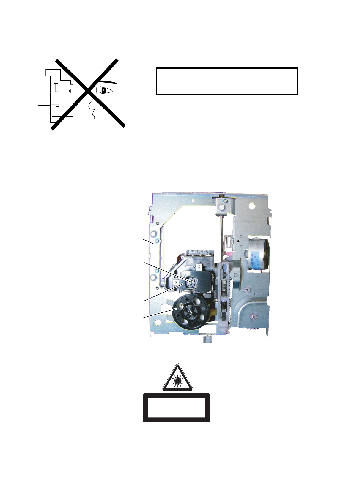
LASER BEAM SAFETY PRECAUTIONS
This DVD player uses a pickup that emits a laser beam.
Do not look directly at the laser beam coming
from the pickup or allow it to strike against your
skin.
The laser beam is emitted from the location shown in the figure. When checking the laser diode, be sure to keep
your eyes at least 30 cm away from the pickup lens when the diode is turned on. Do not look directly at the laser
beam.
CAUTION: Use of controls and adjustments, or doing procedures other than those specified herein, may result in
hazardous radiation exposure.
Drive Mechanism
Assembly
Laser Beam Radiation
Laser Pickup
Turntable
CAUTION- CLASS
-
TION WHEN OPEN. DO NOT VIEW
DIRECTLY WITH OPTICAL INSTRUMENTS
1M
LASER RADIA
-
Location: Top of DVD mechanism.
2-1 E7PLSP
Page 6
IMPORTANT SAFETY PRECAUTIONS
Prior to shipment from the factory, our products are strictly inspected for recognized product safety and electrical
codes of the countries in which they are to be sold. However, in order to maintain such compliance, it is equally
important to implement the following precautions when a set is being serviced.
Safety Precautions for LCD TV
Circuit
1. Before returning an instrument to the
customer, always make a safety check of the
entire instrument, including, but not limited to, the
following items:
a. Be sure that no built-in protective devices are
defective and have been defeated during
servicing. (1) Protective shields are provided
on this chassis to protect both the technician
and the customer. Correctly replace all missing
protective shields, including any removed for
servicing convenience. (2) When reinstalling
the chassis and/or other assembly in the
cabinet, be sure to put back in place all
protective devices, including but not limited to,
nonmetallic control knobs, insulating
fishpapers, adjustment and compartment
covers/shields, and isolation resistor/capacitor
networks. Do not operate this instrument or
permit it to be operated without all
protective devices correctly installed and
functioning. Servicers who defeat safety
features or fail to perform safety checks
may be liable for any resulting damage.
b. Be sure that there are no cabinet openings
through which an adult or child might be able to
insert their fingers and contact a hazardous
voltage. Such openings include, but are not
limited to, (1) spacing between the LCD module
and the cabinet mask, (2) excessively wide
cabinet ventilation slots, and (3) an improperly
fitted and/or incorrectly secured cabinet back
cover.
c. Antenna Cold Check - With the instrument AC
plug removed from any AC source, connect an
electrical jumper across the two AC plug
prongs. Place the instrument AC switch in the
on position. Connect one lead of an ohmmeter
to the AC plug prongs tied together and touch
the other ohmmeter lead in turn to each tuner
antenna input exposed terminal screw and, if
applicable, to the coaxial connector. If the
measured resistance is less than 1.0 megohm
or greater than 5.2 megohm, an abnormality
exists that must be corrected before the
instrument is returned to the customer. Repeat
this test with the instrument AC switch in the off
position.
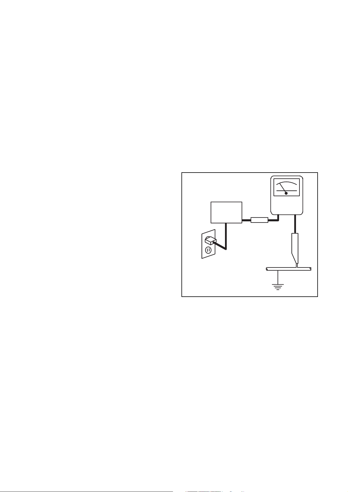
d. Leakage Current Hot Check - With the
instrument completely reassembled, plug the
AC line cord directly into a 230 V AC outlet. (Do
not use an isolation transformer during this
test.) Use a leakage current tester or a
metering system that complies with American
National Standards Institute (ANSI) C101.1
Leakage Current for Appliances and
Underwriters Laboratories (UL) 1410, (50.7).
With the instrument AC switch first in the on
position and then in the off position, measure
from a known earth ground (metal water pipe,
conduit, etc.) to all exposed metal parts of the
instrument (antennas, handle brackets, metal
cabinet, screw heads, metallic overlays, control
shafts, etc.), especially any exposed metal
parts that offer an electrical return path to the
chassis. Any current measured must not
exceed 0.5 milli-ampere. Reverse the
instrument power cord plug in the outlet and
repeat the test.
READING SHOULD
NOT BE ABOVE 0.5 mA
LEAKAGE
DEVICE
BEING
TESTED
TEST ALL EXPOSED
METAL SURFACES
ALSO TEST WITH
PLUG REVERSED
USING AC
ADAPTER PLUG
AS REQUIRED
ANY MEASUREMENTS NOT WITHIN THE
LIMITS SPECIFIED HEREIN INDICATE A
POTENTIAL SHOCK HAZARD THAT MUST
BE ELIMINATED BEFORE RETURNING THE
INSTRUMENT TO THE CUSTOMER OR
BEFORE CONNECTING THE ANTENNA OR
ACCESSORIES.
2. Read and comply with all caution and safety-
related notes on or inside the receiver cabinet, on
the receiver chassis, or on the LCD module.
3. Design Alteration Warning - Do not alter or add
to the mechanical or electrical design of this LCD
TV receiver. Design alterations and additions,
including, but not limited to circuit modifications
and the addition of items such as auxiliary audio
and/or video output connections, might alter the
safety characteristics of this receiver and create a
hazard to the user. Any design alterations or
additions will void the manufacturer's warranty and
may make you, the servicer, responsible for
personal injury or property damage resulting
therefrom.
CURRENT
TESTER
+
EARTH
GROUND
_
3-1 LTVP_ISP
Page 7

4. Hot Chassis Warning -
a. Some TV receiver chassis are electrically
connected directly to one conductor of the AC
power cord and maybe safety-serviced without
an isolation transformer only if the AC power
plug is inserted so that the chassis is
connected to the ground side of the AC power
source. To confirm that the AC power plug is
inserted correctly, with an AC voltmeter,
measure between the chassis and a known
earth ground. If a voltage reading in excess of
1.0V is obtained, remove and reinsert the AC
power plug in the opposite polarity and again
measure the voltage potential between the
chassis and a known earth ground.
b. Some TV receiver chassis normally have 85V
AC(RMS) between chassis and earth ground
regardless of the AC plug polarity. This chassis
can be safety-serviced only with an isolation
transformer inserted in the power line between
the receiver and the AC power source, for both
personnel and test equipment protection.
c. Some TV receiver chassis have a secondary
ground system in addition to the main chassis
ground. This secondary ground system is not
isolated from the AC power line. The two
ground systems are electrically separated by
insulation material that must not be defeated or
altered.
5. Observe original lead dress. Take extra care to
assure correct lead dress in the following areas: a.
near sharp edges, b. near thermally hot parts-be
sure that leads and components do not touch
thermally hot parts, c. the AC supply, d. high
voltage, and, e. antenna wiring. Always inspect in
all areas for pinched, out of place, or frayed wiring.
Check AC power cord for damage.
6. Components, parts, and/or wiring that appear to
have overheated or are otherwise damaged
should be replaced with components, parts, or
wiring that meet original specifications.
Additionally, determine the cause of overheating
and/or damage and, if necessary, take corrective
action to remove any potential safety hazard.
7. Product Safety Notice - Some electrical and
mechanical parts have special safety-related
characteristics which are often not evident from
visual inspection, nor can the protection they give
necessarily be obtained by replacing them with
components rated for higher voltage, wattage, etc..
Parts that have special safety characteristics are
identified by a ! on schematics and in parts lists.
Use of a substitute replacement that does not
have the same safety characteristics as the
recommended replacement part might create
shock, fire, and/or other hazards. The product's
safety is under review continuously and new
instructions are issued whenever appropriate.
Prior to shipment from the factory, our products
are strictly inspected to confirm they comply with
the recognized product safety and electrical codes
of the countries in which they are to be sold.
However, in order to maintain such compliance, it
is equally important to implement the following
precautions when a set is being serviced.
3-2 LTVP_ISP
Page 8

Precautions during Servicing
A. Parts identified by the ! symbol are critical for
safety.
Replace only with part number specified.
B. In addition to safety, other parts and assemblies
are specified for conformance with regulations
applying to spurious radiation. These must also be
replaced only with specified replacements.
Examples: RF converters, RF cables, noise
blocking capacitors, and noise blocking filters, etc.
C. Use specified internal wiring. Note especially:
1) Wires covered with PVC tubing
2) Double insulated wires
3) High voltage leads
D. Use specified insulating materials for hazardous
live parts. Note especially:
1) Insulation Tape
2) PVC tubing
3) Spacers
4) Insulators for transistors.
E. When replacing AC primary side components
(transformers, power cord, etc.), wrap ends of
wires securely about the terminals before
soldering.
F. Observe that the wires do not contact heat
producing parts (heat sinks, oxide metal film
resistors, fusible resistors, etc.)
G. Check that replaced wires do not contact sharp
edged or pointed parts.
H. When a power cord has been replaced, check that
5~6 kg of force in any direction will not loosen it.
I. Also check areas surrounding repaired locations.
J. Use care that foreign objects (screws, solder
droplets, etc.) do not remain inside the set.
K. Crimp type wire connector
The power transformer uses crimp type
connectors which connect the power cord and the
primary side of the transformer. When replacing
the transformer, follow these steps carefully and
precisely to prevent shock hazards.
Replacement procedure
1) Remove the old connector by cutting the wires
at a point close to the connector.
Important: Do not re-use a connector (discard
it).
2) Strip about 15 mm of the insulation from the
ends of the wires. If the wires are stranded,
twist the strands to avoid frayed conductors.
3) Align the lengths of the wires to be connected.
Insert the wires fully into the connector.
4) Use the crimping tool to crimp the metal sleeve
at the center position. Be sure to crimp fully to
the complete closure of the tool.
L. When connecting or disconnecting the internal
connectors, first, disconnect the AC plug from the
AC supply outlet.
M. When installing parts or assembling the cabinet
parts, be sure to use the proper screws and
tighten certainly.
3-3 LTVP_ISP
Page 9
Safety Check after Servicing
Examine the area surrounding the repaired location
for damage or deterioration. Observe that screws,
parts and wires have been returned to original positions. Afterwards, perform the following tests and confirm the specified values in order to verify compliance
with safety standards.
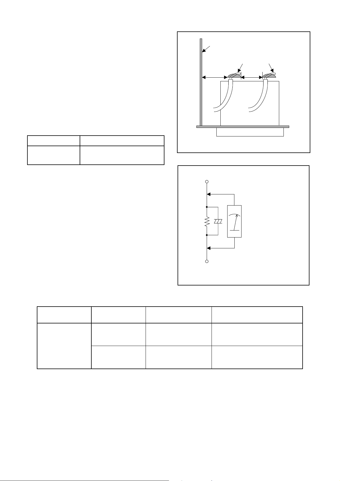
1. Clearance Distance
When replacing primary circuit components, confirm
specified clearance distance (d) and (d') between soldered terminals, and between terminals and surrounding metallic parts. (See Fig. 1)
Table 1 : Ratings for selected area
AC Line Voltage Clearance Distance (d), (d’)
230 V
Note: This table is unofficial and for reference only.
Be sure to confirm the precise values.
≥ 3mm(d)
≥ 6 mm(d’)
2. Leakage Current Test
Confirm the specified (or lower) leakage current between B (earth ground, power cord plug prongs) and
externally exposed accessible parts (RF terminals, antenna terminals, video and audio input and output terminals, microphone jacks, earphone jacks, etc.).
Chassis or Secondary Conductor
Primary Circuit
d' d
Exposed Accessible Part
Z
AC Voltmeter
(High Impedance)
Fig. 1
Measuring Method : (Power ON)
Insert load Z between B (earth ground, power cord
plug prongs) and exposed accessible parts. Use an
AC voltmeter to measure across both terminals of load
Z. See Fig. 2 and following table.
Table 2: Leakage current ratings for selected areas
AC Line Voltage Load Z Leakage Current (i)
2kΩ RES.
Connected in
parallel
230 V
50kΩ RES.
Connected in
parallel
Note: This table is unofficial and for reference only. Be sure to confirm the precise values.
i≤0.7mA AC Peak
i≤2mA DC
i≤0.7mA AC Peak
i≤2mA DC
One side of
B
Power Cord Plug Prongs
One side of power cord plug
prongs (B) to:
Antenna terminals
A/V Input, Output
Fig. 2
RF or
3-4 LTVP_ISP
Page 10
STANDARD NOTES FOR SERVICING
Circuit Board Indications
1. The output pin of the 3 pin Regulator ICs is
indicated as shown.
Top View
Out
2. For other ICs, pin 1 and every fifth pin are
indicated as shown.
Pin 1
3. The 1st pin of every male connector is indicated as
shown.
Input
In
Bottom View
5
10
Pb (Lead) Free Solder
Pb free mark will be found on PCBs which use Pb
free solder. (Refer to figure.) For PCBs with Pb free
mark, be sure to use Pb free solder. For PCBs
without Pb free mark, use standard solder.
Pb free mark
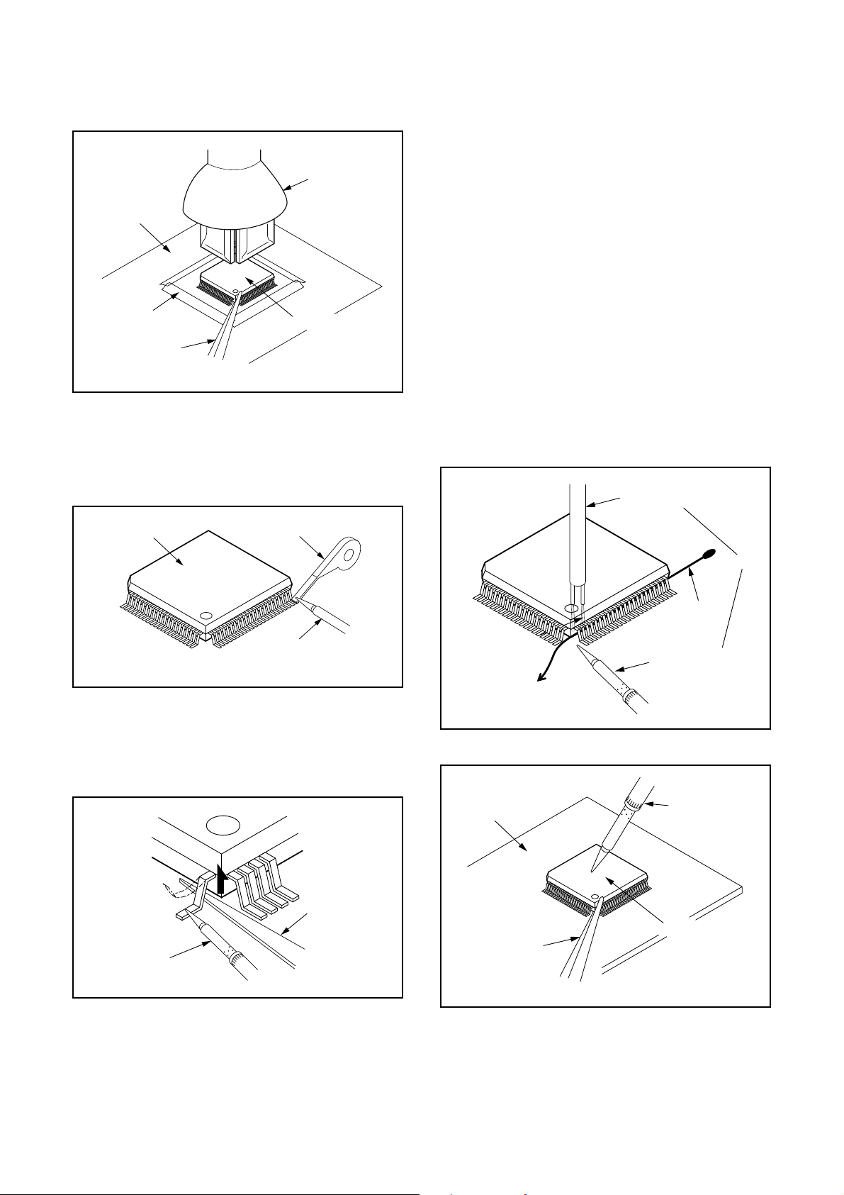
How to Remove / Install Flat Pack-IC
1. Removal
With Hot-Air Flat Pack-IC Desoldering Machine:
1. Prepare the hot-air flat pack-IC desoldering
machine, then apply hot air to the Flat Pack-IC
(about 5 to 6 seconds). (Fig. S-1-1)
Pin 1
Instructions for Connectors
1. When you connect or disconnect the FFC (Flexible
Foil Connector) cable, be sure to first disconnect
the AC cord.
2. FFC (Flexible Foil Connector) cable should be
inserted parallel into the connector, not at an
angle.
FFC Cable
Connector
CBA
* Be careful to avoid a short circuit.
Fig. S-1-1
2. Remove the flat pack-IC with tweezers while
applying the hot air.
3. Bottom of the flat pack-IC is fixed with glue to the
CBA; when removing entire flat pack-IC, first apply
soldering iron to center of the flat pack-IC and heat
up. Then remove (glue will be melted). (Fig. S-1-6)
4. Release the flat pack-IC from the CBA using
tweezers. (Fig. S-1-6)
CAUTION:
1. The Flat Pack-IC shape may differ by models. Use
an appropriate hot-air flat pack-IC desoldering
machine, whose shape matches that of the Flat
Pack-IC.
2. Do not supply hot air to the chip parts around the
flat pack-IC for over 6 seconds because damage
to the chip parts may occur. Put masking tape
around the flat pack-IC to protect other parts from
damage. (Fig. S-1-2)
4-1 TVP_SN
Page 11
3. The flat pack-IC on the CBA is affixed with glue, so
be careful not to break or damage the foil of each
pin or the solder lands under the IC when
removing it.
Hot-air
Flat Pack-IC
Desoldering
CBA
Masking
Tape
Machine
Flat Pack-IC
Tweezers
Fig. S-1-2
With Soldering Iron:
1. Using desoldering braid, remove the solder from
all pins of the flat pack-IC. When you use solder
flux which is applied to all pins of the flat pack-IC,
you can remove it easily. (Fig. S-1-3)
With Iron Wire:
1. Using desoldering braid, remove the solder from
all pins of the flat pack-IC. When you use solder
flux which is applied to all pins of the flat pack-IC,
you can remove it easily. (Fig. S-1-3)
2. Affix the wire to a workbench or solid mounting
point, as shown in Fig. S-1-5.
3. While heating the pins using a fine tip soldering
iron or hot air blower, pull up the wire as the solder
melts so as to lift the IC leads from the CBA
contact pads as shown in Fig. S-1-5.
4. Bottom of the flat pack-IC is fixed with glue to the
CBA; when removing entire flat pack-IC, first apply
soldering iron to center of the flat pack-IC and heat
up. Then remove (glue will be melted). (Fig. S-1-6)
5. Release the flat pack-IC from the CBA using
tweezers. (Fig. S-1-6)
Note: When using a soldering iron, care must be
taken to ensure that the flat pack-IC is not
being held by glue. When the flat pack-IC is
removed from the CBA, handle it gently
because it may be damaged if force is applied.
Hot Air Blower
Flat Pack-IC
Desoldering Braid
Soldering Iron
Fig. S-1-3
2. Lift each lead of the flat pack-IC upward one by
one, using a sharp pin or wire to which solder will
not adhere (iron wire). When heating the pins, use
a fine tip soldering iron or a hot air desoldering
machine. (Fig. S-1-4)
Sharp
Pin
Fine Tip
Soldering Iron
Fig. S-1-4
To Solid
Mounting Point
CBA
Tweezers
or
Iron Wire
Soldering Iron
Fig. S-1-5
Fine Tip
Soldering Iron
Flat Pack-IC
Fig. S-1-6
3. Bottom of the flat pack-IC is fixed with glue to the
CBA; when removing entire flat pack-IC, first apply
soldering iron to center of the flat pack-IC and heat
up. Then remove (glue will be melted). (Fig. S-1-6)
4. Release the flat pack-IC from the CBA using
tweezers. (Fig. S-1-6)
4-2 TVP_SN
Page 12
2. Installation
1. Using desoldering braid, remove the solder from
the foil of each pin of the flat pack-IC on the CBA
so you can install a replacement flat pack-IC more
easily.
2. The “●” mark on the flat pack-IC indicates pin 1.
(See Fig. S-1-7.) Be sure this mark matches the 1
on the PCB when positioning for installation. Then
presolder the four corners of the flat pack-IC. (See
Fig. S-1-8.)
3. Solder all pins of the flat pack-IC. Be sure that
none of the pins have solder bridges.
Example :
Pin 1 of the Flat Pack-IC
is indicated by a " " mark.
Fig. S-1-7
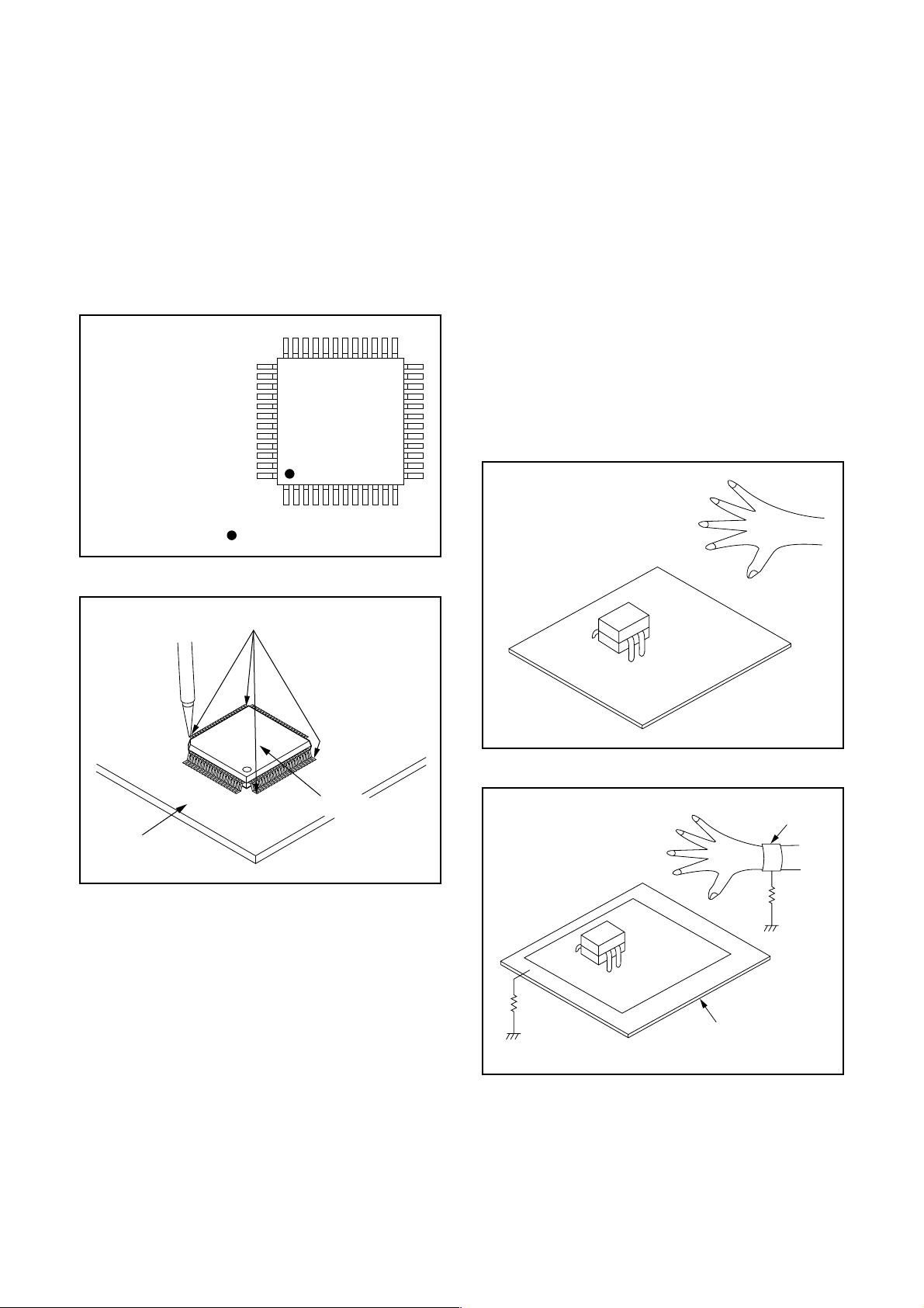
Instructions for Handling Semiconductors
Electrostatic breakdown of the semi-conductors may
occur due to a potential difference caused by
electrostatic charge during unpacking or repair work.
1. Ground for Human Body
Be sure to wear a grounding band (1 MΩ) that is
properly grounded to remove any static electricity that
may be charged on the body.
2. Ground for Workbench
Be sure to place a conductive sheet or copper plate
with proper grounding (1 MΩ) on the workbench or
other surface, where the semi-conductors are to be
placed. Because the static electricity charge on
clothing will not escape through the body grounding
band, be careful to avoid contacting semi-conductors
with your clothing.
<Incorrect>
CBA
Presolder
Flat Pack-IC
Fig. S-1-8
<Correct>
1MΩ
CBA
Grounding Band
1MΩ
CBA
Conductive Sheet or
Copper Plate
4-3 TVP_SN
Page 13
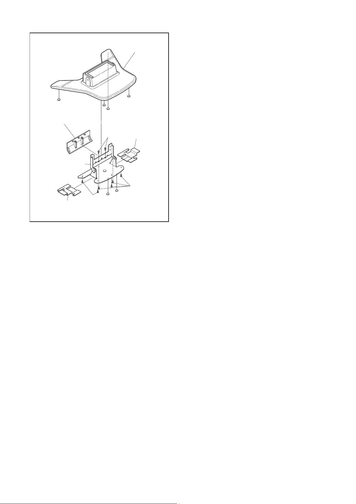
CABINET DISASSEMBLY INSTRUCTIONS
1. Disassembly Flowchart
This flowchart indicates the disassembly steps for the
cabinet parts, and the CBA in order to gain access to
item(s) to be serviced. When reassembling, follow the
steps in reverse order. Bend, route and dress the
cables as they were.
[14] Speaker(s)
[8] Inverter CBA
[3] Jack Holder
[12] Function
CBA
[2] Rear Cabinet
[4] DVD Main
CBA Unit
[5] DVD
Mechanism
[6] DVD
Holder(L)
[7] DVD
Holder(R)
[9] Main CBA
[10] Tilt Stand
Holder
[11] LCD Main
CBA Unit &
Liquid Crystal
Panel Unit
[15] Front
Cabinet
[13] IR Sensor
CBA
[1] Tilt Stand
Assembly
[16] Stand Cover
[17] Arm Holder
[18] Sheet L, R
[19] Arm
Assembly
2. Disassembly Method
Removal
Step/
Loc.
No.
[1]
Part
Tilt Stand
Assembly
Remove/*Unhook/
Fig.
No.
Unlock/Release/
Unplug/Unclamp/
Note
Desolder
D1 4(S-1) ---
Removal
Step/
Loc.
No.
Part
Remove/*Unhook/
Fig.
No.
Unlock/Release/
Unplug/Unclamp/
Note
Desolder
DVD
[7]
[8]
Holder(R)
Inverter
CBA
D2 2(S-9) ---
4(S-10), *CN301,
D3
*CN302, *CN303,
D6
*CN304, *CN310
8(S-11), *CN53,
D3
[9] Main CBA
*CN801, *CN101B,
D6
*CN102B, *CN103B,
*CN1651
Tilt Stand
[10]
Holder
D3 2(S-12) ---
LCD Main
[11]
CBA Unit &
Liquid
Crystal
D4
13(S-13), *CN106 ---
D6
Panel Unit
Function
[12]
CBA
IR Sensor
[13]
CBA
[14] Speaker(s) D4
Front
[15]
Cabinet
Stand
[16]
Cover
D4 5(S-14) ---
D4 (S-15) ---
4(S-16), Speaker
Holder (s)
D4 --------------- ---
D5 6(S-17) ---
[17] Arm Holder D5 2(S-18) ---
[18] Sheet L, R D5 --------------- ---
Arm
[19]
↓
(1)
Assembly
↓
(2)
D5 --------------- ---
↓
(3)
↓
(4)
---
---
---
↓
(5)
Rear
[2]
Cabinet
D1 9(S-2), 2(S-3) ---
[3] Jack Holder D2 (S-4), 3(S-5) ---
DVD Main
[4]
CBA UnitD2D6
(S-6), *CN201,
*CN301, *CN401,
*CN601, *CN801
1
2
DVD
[5]
Mechanism
D2 4(S-7)
3
4
5
DVD
[6]
Holder(L)
D2 2(S-8) ---
5-1 L4670DC
Page 14

Note:
(1) Order of steps in procedure. When reassembling,
follow the steps in reverse order. These numbers
are also used as the Identification (location) No. of
parts in figures.
(2) Parts to be removed or installed.
(3) Fig. No. showing procedure of part location
(4) Identification of parts to be removed, unhooked,
unlocked, released, unplugged, unclamped, or
desoldered.
P = Spring, L = Locking Tab, S = Screw,
CN = Connector
* = Unhook, Unlock, Release, Unplug, or Desolder
e.g. 2(S-2) = two Screws (S-2),
2(L-2) = two Locking Tabs (L-2)
(5) Refer to the following "Reference Notes in the
Table."
Reference Notes
1. CAUTION 1: Electrostatic breakdown of the laser
diode in the optical system block may occur as a
potential difference caused by electrostatic charge
accumulated on cloth, human body etc., during
unpacking or repair work.
To avoid damage of pickup follow next procedures.
1) Short the three short lands of FPC cable with
solder before removing the FFC cable (CN201)
from it. If you disconnect the FFC cable
(CN201), the laser diode of pickup will be
destroyed. (Fig. D2)
2) Disconnect Connectors (CN301), (CN401),
(CN601) and (CN801). Remove three Screws
(S-6) and remove the DVD Main CBA Unit.
(Fig. D2)
2. Reassembly Notes of New DVD Mechanism:
a. To remove the Chassis Cover, remove two
screws A as shown in Fig. D2.
b. To avoid damage of the pickup unit (laser
diode), confirm that the three short lands (either
of two places) are shorted out by soldering
between them as shown in View A in Fig. D2.
c. Connect the FFC cables of the new DVD
Mechanism to the three connectors (CN201,
CN301, CN801) on the DVD Main CBA Unit.
d. After confirming that the FFC cables are
securely connected to the three connectors,
remove the solder from the three short lands. If
the solder is not removed, the laser diode will
not light and it will not be possible to read discs.
e. Insert the pin A on the Chassis Cover into the
hole A on the Main Chassis as shown in Fig.
D2. Then tighten two screws A to install the
Chassis Cover.
3. CAUTION 2: When reassembling, confirm the
FFC cable (CN201) is connected completely. Then
remove the solder from the three short lands of
FPC cable. (Fig. D2)
4. How to eject a disc in emergency
Press and hold [EJECT] on the unit for more than
5 seconds.
5. How to eject manually
1) Remove the Rear Cabinet and DVD Cover.
2) To remove the DVD Main CBA Unit, remove a
screw (S-6) in Fig. D2. Do not disconnect
connectors.
3) To remove the Chassis Cover, remove two
screws A as shown in Fig. D2.
4) Remove a disc
5-2 L4670DC
Page 15
[2] Rear Cabinet
[1] Tilt Stand
Assembly
(S-2)
(S-3)
(S-2)
(S-2)
(S-3)
(S-2)
(S-1)
Fig. D1
5-3 L4670DC
Page 16
(S-5)
[6] DVD Holder (L)
[5] DVD Mechanism
(S-8)
(S-9)
(S-4)
[3] Jack Holder
(S-7)
[7] DVD Holder (R)
(S-7)
(S-5)
A
(S-7)
(S-6)
[4] DVD Main CBA Unit
Remove two screws A, then short the three short lands by soldering as shown in View for A.
Chassis Cover
Pin A
Either of two places
A
Screws A
FPC Cable
View for A
Hole A
Main Chassis
Fig. D2
5-4 L4670DC
Page 17
(S-10)
[10]Tilt Stand Holder
[15] Front Cabinet
(S-12)
(S-11)
[9] Main CBA
(S-11)
(S-11)
[8] Inverter CBA
(S-10)
Fig. D3
(S-14)
[14] Speaker
Speaker Holders
(S-16)
(S-16)
[14] Speaker
[13] IR Sensor CBA
(S-15)
[11] LCD Main CBA Unit &
Liquid Crystal Panel Unit
[12] Function CBA
(S-14)
(S-14)
Speaker Holders
(S-13)
(S-13)
(S-13)
(S-13)
(S-13)
Fig. D4
5-5 L4670DC
Page 18
[17] Arm Holder
[16] Stand Cover
[19] Arm
Assembly
[18] Sheet L
(S-17)
(S-18)
[18] Sheet R
(S-17)
Fig. D5
5-6 L4670DC
Page 19
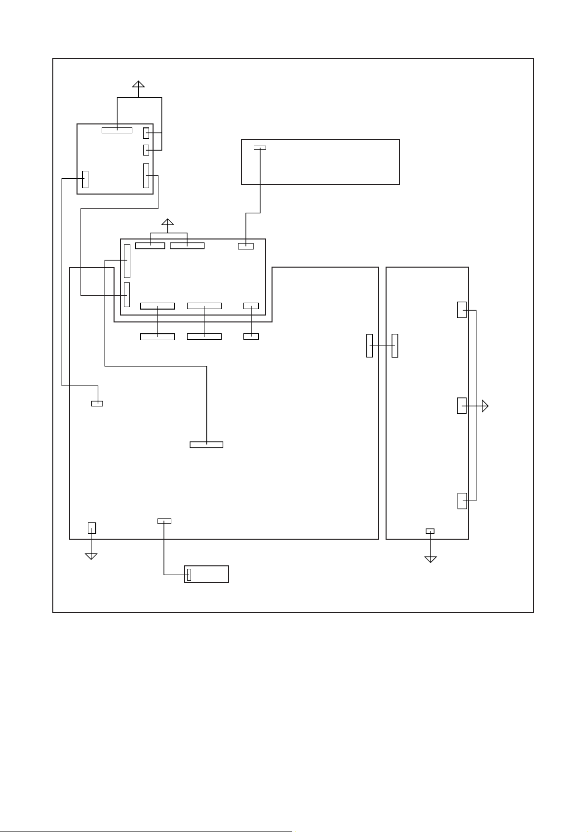
TV Cable Wiring Diagram
To DVD Mechanism
DVD Main
CBA Unit
CN201
CN601
CN301
CN801
CN401
LCD Main
CBA Unit
To Liquid Crystal
Panel Unit
Function CBA
CLN904
CN801
CN1701
CN311 CN312
CN1751
CN1761
CN103B
CN103A
CN53
CN102B
CN102A
CN1651
CN106
CN101B
CN101A
Main CBA
CN404
Inverter CBA
CN301
CN304
CN302
CN303
CN310
To
Liquid
Crystal
Panel
Unit
To Speaker
IR Sensor CBA
CLN53
To Speaker
Fig. D6
5-7 L4670DC
Page 20
ELECTRICAL ADJUSTMENT INSTRUCTIONS
General Note:
“CBA” is abbreviation for “Circuit Board Assem-
bly.”
NOTE:
Electrical adjustments are required after replacing
circuit components and certain mechanical parts. It is
important to perform these adjustments only after all
repairs and replacements have been completed.
Also, do not attempt these adjustments unless the
proper equipment is available.
Test Equipment Required
1. DC Voltmeter
2. Pattern Generator
3. Color Analyzer
How to Set up the Service mode:
1. Turn the power on. (Use main power on the TV
unit.)
2. Press [STANDBY], [2], [7], [1], and [MUTE] buttons
on the remote control unit in that order within 5
seconds.
- To cancel the service mode, press [STANDBY]
button on the remote control.
1. Initial Setting
General
Enter the Service mode.
Set the each initial data as shown on table 1 below.
Table 1: Initial Data
BUTTON
ITEM
BRT(PAL)
CNT(PAL) 140
CLR-R(PAL) 70
CLR-B(PAL) 70
SHR(PAL) 143
S-BRT(PAL)
S-CNT(PAL) 140
S-CLR-R(PAL) 70
S-CLR-B(PAL) 70
S-SHR(PAL) 143
C-BRT(PAL)
C-CNT(PAL) 128
C-CLR-R(PAL) 120
C-CLR-B(PAL) 120
C-SHR(PAL) 143
BRT(SECAM)
CNT(SECAM) 140
CLR-R(SECAM) 70
CLR-B(SECAM) 70
SHR(SECAM) 143
S-BRT(SECAM)
S-CNT(SECAM) 140
S-CLR-R(SECAM) 70
S-CLR-B(SECAM) 70
S-SHR(SECAM) 143
C-BRT(SECAM)
C-CNT(SECAM) 128
C-CLR-R(SECAM) 120
C-CLR-B(SECAM) 120
C-SHR(SECAM) 143
BRT(NTSC)
CNT(NTSC) 138
CLR-R(NTSC) 77
CLR-B(NTSC) 77
TNT(NTSC) 120
SHR(NTSC) 143
S-BRT(NTSC)
S-CNT(NTSC) 138
S-CLR-R(NTSC) 74
S-CLR-B(NTSC) 74
S-TNT(NTSC) 120
S-SHR(NTSC) 143
(on the remote
control)
MENU → 1
MENU → 2
MENU → 3
MENU → 4
MENU → 5
MENU → 6
MENU → 7
MENU → 8
DATA
VALUE
130
133
128
130
133
128
128
128
6-1 L4670EA
Page 21
BUTTON
ITEM
C-BRT(NTSC)
C-CNT(NTSC) 128
C-CLR-R(NTSC) 150
C-CLR-B(NTSC) 150
C-TNT(NTSC) 120
C-SHR(NTSC) 143
BRIGHT 0 0
NORMAL 0 65
DARK 0 98
COR(C/D/S-1) VOL. p → 1 128
COG(C/D/S-1) VOL. p → 2 128
COB(C/D/S-1) VOL. p → 3 128
DR(C/D/S-1) VOL. p → 4 180
DG(C/D/S-1) VOL. p → 5 180
DB(C/D/S-1) VOL. p → 6 180
SBR(C/D/S-1) VOL. p → 70
SBB(C/D/S-1) VOL. p → 90
C-COR(C/D/S-2) VOL. p → 1 128
C-COG(C/D/S-2) VOL. p → 2 128
C-COB(C/D/S-2) VOL. p → 3 128
C-DR(C/D/S-2) VOL. p → 4 140
C-DG(C/D/S-2) VOL. p → 5 140
C-DB(C/D/S-2) VOL. p → 6 140
C-SBR(C/D/S-2) VOL. p → 70
C-SBB(C/D/S-2) VOL. p → 90
7F
LAST POWER OFF
SYSTEM *1
NCM ON
ASPECT OFF
RUSSIAN OFF
(on the remote
control)
MENU → 9
VOL. p
DATA
VALUE
128
FF
2. Flicker Adjustment
1. Enter the Service mode. (See page 6-1.)
2. Press [2] button on the remote control unit.
The following screen appears.
VCOM
128
3. If Flicker Adjustment is not fit, the screen becomes
the following.
VCOM
128
FLASH (Go and Off)
4. Press [CH. o / p] buttons on the remote control
unit so that flash stops.
*1 PAL-BG (LDD-A2006), PAL-I (LDD-B2006),
SECAM-L (LDD-C2006), PAL-BG/DK (LDD-D2006)
6-2 L4670EA
Page 22
The following adjustment normally are not
attempted in the field. Only when replacing the
LCD Panel then adjust as a preparation.
3. White Balance Adjustment
Purpose: To mix red, green and blue beams correctly
for pure white.
Symptom of Misadjustment: White becomes bluish
or reddish.
Test Point Adj. Point Mode Input
[RF/AV2(CVBS)]
Screen
VOL. p
buttons
M. EQ. Spec.
C/D/S-1
[AV1(RGB)]
C/D/S-2
White Purity
(APL 80%)
or
(APL 40%)
6. [AV1(RGB)]----(APL 80%)
Press [6] button to select “C-DB(C/D/S-2)” for Blue
adjustment. Press [4] button to select “C-DR(C/D/
S-2)” for Red adjustment.When “x” value and “y”
value are not within specification, adjust “C-DB(C/
D/S-2)” or “C-DR(C/D/S-2)”. Refer to “1. Initial
Setting.”
[AV1(RGB)]----(APL 40%)
Press [3] button to select “C-COB(C/D/S-2)” for
Blue adjustment. Press [1] button to select “CCOR(C/D/S-2)” for Red adjustment.When “x”
value and “y” value are not within specification,
a d j u s t “ C - C O B ( C / D / S - 2 ) ” o r “ C - C O R ( C / D / S - 2 ) ” .
Refer to “1. Initial Setting.”
7. Turn the power off and on again. (Main power
button on the TV unit.)
Pattern Generator,
Color analyzer
Figure
x: 285 to 295,
y: 295 to 305
It carries out in a darkroom.
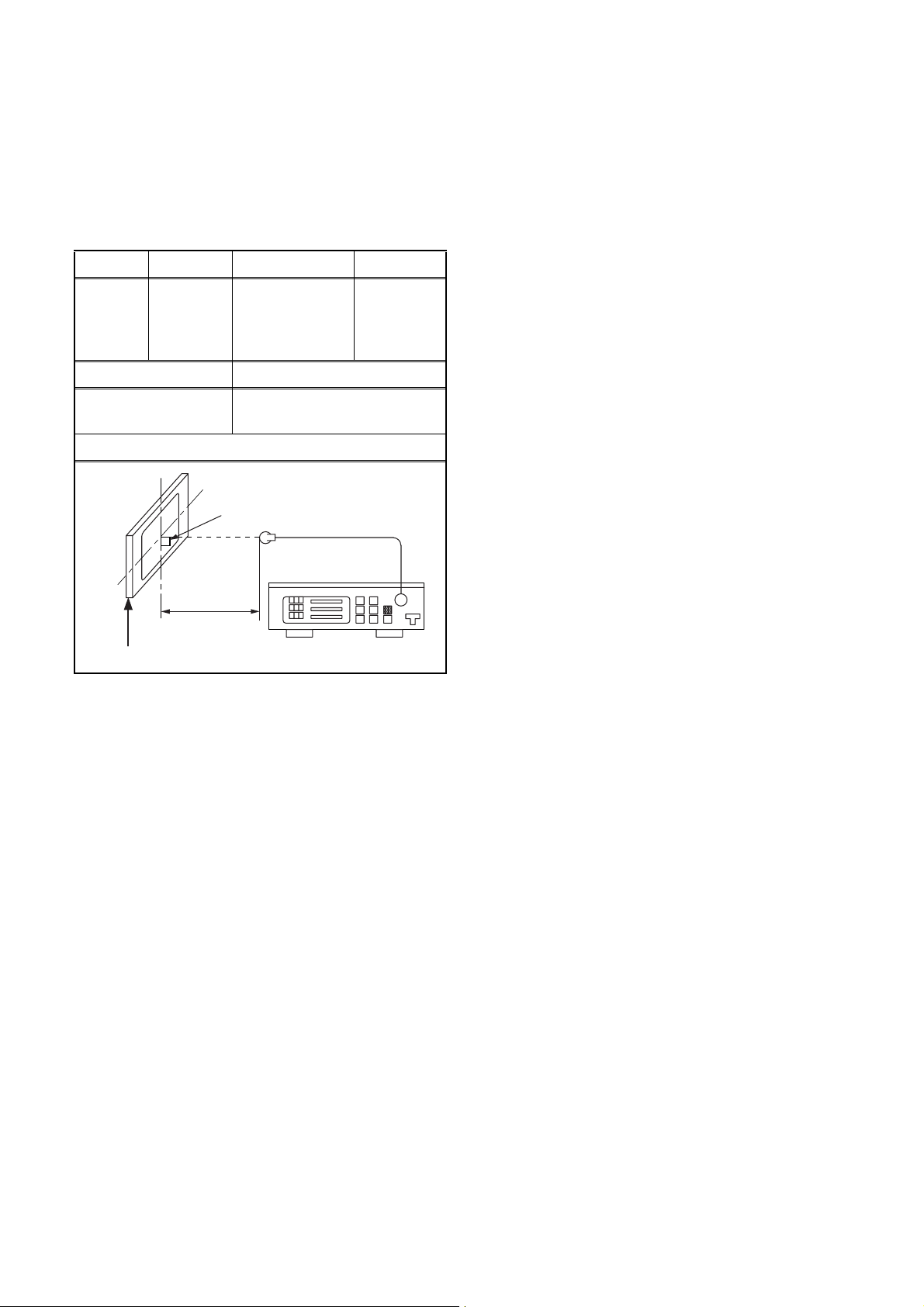
Perpendicularity
L = 3 cm
INPUT: WHITE 80%
1. Operate the unit for more than 20 minutes.
2. Input the White Purity.
3. Set the color analyzer to the CHROMA mode and
bring the optical receptor to the center on the
LCD-Panel surface after zero point calibration as
shown above.
Note: The optical receptor must be set
perpendicularly to the LCD Panel surface.
4. [RF/AV2(CVBS)]
Enter the Service mode. Press [VOL p] button on
the remote control unit and select “C/D/S-1” mode.
[AV1(RGB)]
Enter the Service mode. Press [VOL p] button on
the remote control unit and select “C/D/S-2” mode.
5. [RF/AV2(CVBS)]----(APL 80%)
Press [6] button to select “DB(C/D/S-1)” for Blue
adjustment. Press [4] button to select “DR(C/D/S-
1)” for Red adjustment. When “x” value and “y”
value are not within specification, adjust “DB (C/D/
S-1)” or “DR (C/D/S-1)”. Refer to “1. Initial Setting.”
[RF/AV2(CVBS)]----(APL 40%)
Press [3] button to select “COB(C/D/S-1)” for Blue
adjustment. Press [1] button to select “COR(C/D/
S-1)” for Red adjustment. When “x” value and “y”
value are not within specification, adjust “COB (C/
D/S-1)” or “COR (C/D/S-1)”. Refer to “1. Initial
Setting.”
Color Analyzer
6-3 L4670EA
Page 23

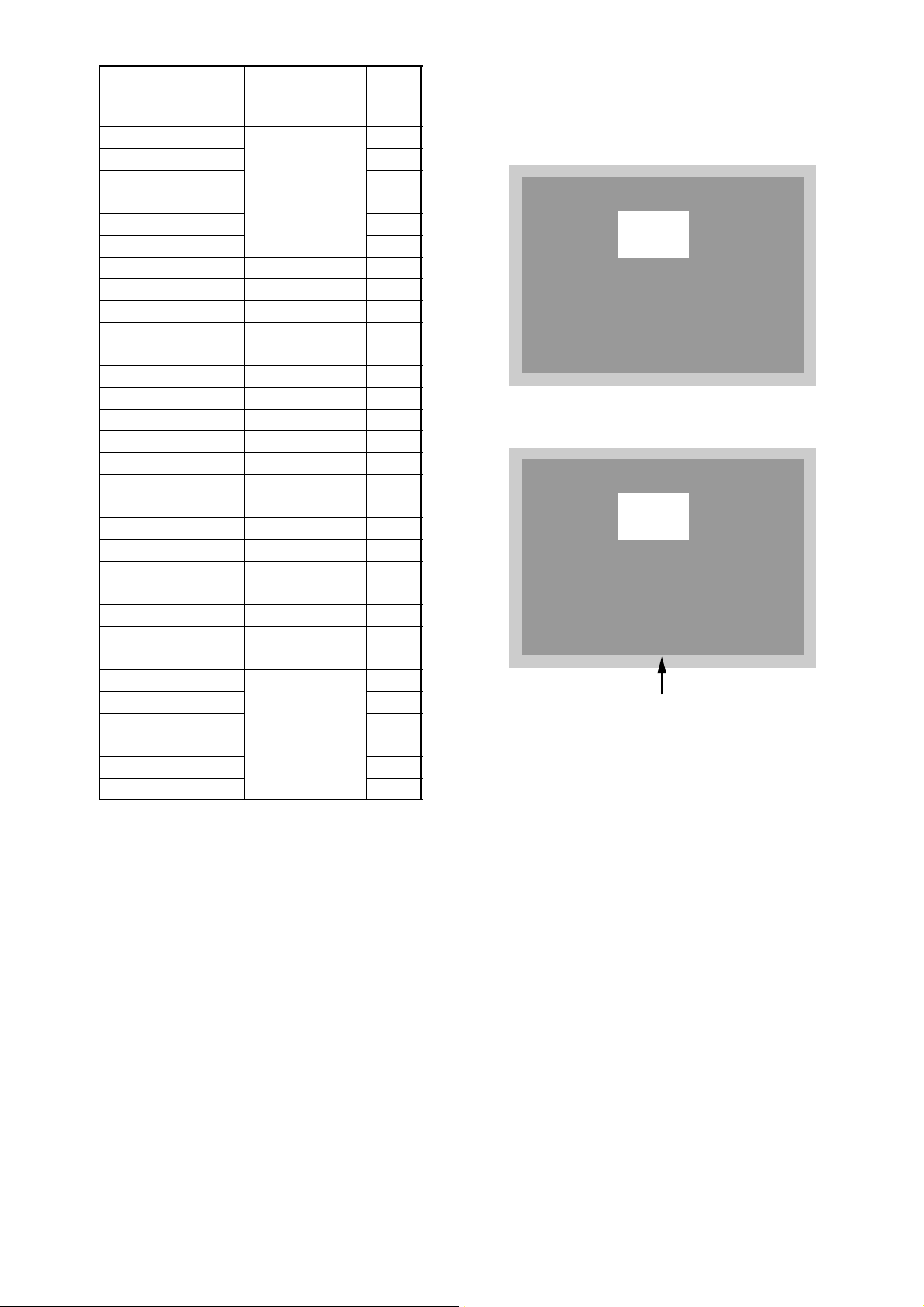
HOW TO INITIALIZE THE LCD TV/DVD
To put the program back at the factory-default, initialize the LCD TV/DVD as the following procedure.
< DVD Section >
1. Press [1], [2], [3], [4], and [DISPLAY] buttons on the
remote control unit in that order.
Fig. g appears on the screen.
"
" differs depending on the models.
*******
MODEL : *******
Version
Region
Version
Region
: *.**
: *
EXIT: SELECTEEPROM CLEAR : CLEAR
Fig. g
"
" differs depending on the models.
*******
: *.**
: *
2. Press [CLEAR] button on the remote control unit.
Fig. h appears on the screen.
MODEL : *******
< LCD TV Section >
1. Turn the power on. (Use main power on the TV
unit.)
2. To enter the service mode, press [STANDBY], [2],
[7], [1], and [MUTE] buttons on the remote control
unit in that order within 5 seconds.
- To cancel the service mode, press [STANDBY]
button on the remote control.
3. To initialize the LCD television, press “DISPLAY”
button on the remote control unit.
4. Confirm "FF" indication on the upper right of the
screen.
EEPROM CLEAR : OK
EXIT: SELECTEEPROM CLEAR : CLEAR
Fig. h
When “OK” appears on the screen, the factory
default will be set.
3. To exit this mode, press [CH. o / p] or [SELECT]
button to go to TV mode, or press [STANDBY] button to turn the power off.
7-1 L4670INT
Page 24

FIRMWARE RENEWAL MODE
1. Turn the power on and press [EJECT] button on the
remote control unit to put the LCD TV/DVD into
DVD mode. Then remove the disc.
2. To put the LCD TV/DVD into F/W version up mode,
press [9], [8], [7], [6], and [MODE] buttons on the
remote control unit in that order.
Fig. a appears on the screen.
"
" differs depending on the models.
*******
F/W Version Up Mode Model No : *******
Please insert a DISC
for F/W Version Up.
VERSION : *.**
EXIT: SELECT
Fig. a Version Up Mode Screen
3. Insert the disc for version up into the disc slot.
4. The LCD TV/DVD enters the F/W version up mode
automatically. Fig. c appears on the screen. If you
enter the F/W for different models, “Disc Error” will
appear on the screen, then the disc will be ejected
automatically.
"
" differ depending on the models.
*******
(*1)
F/W Version Up Mode Model No : *******
VERSION : ************.ab7
Reading...
VERSION : *.**
6. Remove the disc.
7. Press [CH. o / p] button on the unit to go to TV
mode, or press [STANDBY] button on the unit to
turn the power off.
8. Press [EJECT] button on the remote control unit to
put the LCD TV/DVD into DVD mode again.
9. Press [1], [2], [3], [4], and [DISPLAY] buttons on the
remote control unit in that order.
Fig. g appears on the screen.
"
" differs depending on the models.
*******
MODEL : *******
Version
Region
: *.**
: *
EXIT: SELECTEEPROM CLEAR : CLEAR
Fig. g
10.Press [CLEAR] button on the remote control unit.
Fig. h appears on the screen.
"
" differs depending on the models.
*******
MODEL : *******
Version
Region
: *.**
: *
EEPROM CLEAR : OK
Fig. c Programming Mode Screen
The appearance shown in (*1) of Fig. c is
described as follows:
AppearanceNo. State
Reading... Sending files into the memory
1
Erasing... Erasing previous version data
2
Programming...
3 Writing new version data
5. After programming is finished, the disc will be
ejected automatically. Fig. e appears on the screen
and the checksum will be shown in (*2).
"
" differ depending on the models.
*******
(*2)
F/W Version Up Mode
VERSION : ************.ab7
Completed
SUM : 7ABC
Model No : *******
VERSION : *.**
EXIT: SELECTEEPROM CLEAR : CLEAR
Fig. h
When “OK” appears on the screen, the factory
default will be set. Then the firmware renewal
mode is complete.
11.To exit this mode, press [CH. o / p] or [SELECT]
button to go to TV mode, or press [STANDBY]
button to turn the power off.
Fig. e Completed Program Mode Screen
At this time, no button is available.
8-1 L4670INT
Page 25

BLOCK DIAGRAMS < LCD TV SECTION >
System Control Block Diagram
AL+5V
DVD-CS
DVD-SCLK
DVD-SDATA
TO SYSTEM CONTROL
/SERVO BLOCK DIAGRAM
<DVD SECTION>
DISC-OUT
LED-CONT
DVD-REMOTE
FUNCTION CBA
KEY SWITCH
KEY SWITCH
CLN904
KEY-IN-122
KEY-IN-211
CN106
DISC-IN
POWER
IR SENSOR CBA
D51
SENSOR
REMOTE
RCV51
CLN53
RCV-IN33
CN53
TO POWER SUPPLY
TO LCD BACKLIGHT
PROTECT-1
BACKLIGHT-ADJ
CN102A
RCV-IN11
BLOCK DIAGRAM
BLOCK DIAGRAM
P-DOWN
P-25V-ON
PWRCON
PROTECT-1
PROTECT-2
DVD-MAIN-P
BACKLIGHT-ADJ
P-ON-H66
PROTECT-113 13
PROTECT-214 14
DVD-MAIN-P
22
P-DOWN44
22 22
TO IF/VIDEO
SCL
SDA
S-SW
AFT-IN
INPUT-0
S/C-JACK-MUTE
VOLUME77
INPUT-099
S-SW15 15
INPUT-110 10
SCL18 18
SDA19 19
DVD-MUTE33
BLOCK DIAGRAM
INPUT-1
FBIN
SLOW-SW
RAPID-SW
SLOW-SW17 17
RAPID-SW16 16
P-25V-ON21 21
SP-MUTE
INSEL-MUTE
S/C-JACK-MUTE
INSEL-MUTE
S/C-JACK-MUTE
15 15
14 14
TO AUDIO
BLOCK DIAGRAM
SCL
SDA
NICAM-RESET
NICAM-RESET
SP-MUTE18 18
FBIN22 22
DVD-H19 19
20 20
VOLUME
DVD-MUTE
DVD-H
MAIN CBALCD MAIN CBA UNIT
76
75
DVD-CS
DVD-SCLK
XIN
XOUT
IC151
(MICRO COMPUTER)
13
11
X151
10MHz
CN301(NO CONNECTION)
5
DVP-RESET-PC8DVP-CLK-PC
DVP-SOUT-PC6DVP-SIN-PC7DVP-CS-PC4MPSEL-0 3
74
DVD-SDATA
67
65
LED-CONT
DVD-REMOTE
BUS-OPEN 2
63
64
DISC-IN
DISC-OUT
VCOM
VCOM
20
TO LCD
BLOCK DIAGRAM
83
MPSEL-0
LCD DRIVE / LCD
SIGNAL PROCESS
IC301
2DVP-RESET
79
AL+3.3V
3.3V<-->5V
Q152
RESET
2DVP-CLK
5
CONVERTER
Q153
57
MPWEH
92
KEY-IN-2
2DVP-SIN
4
3.3V<-->5V
CONVERTER
Q154
59
MPOE
CN102B
93
16
RCV-IN
KEY-IN-1
2DVP-SOUT
3
3.3V<-->5V
CONVERTER
Q155
585060
MPWEL
895922
26
PROTECT-1
BUS-OPENV
BACKLIGHT-ADJ
2DVP-CS
2
3.3V<-->5V
CONVERTER
Q156
MPCE
RESET
Q157
10
88
RESET
P-ON-H
PROTECT-2
H-SYNC
25
3.3V<-->5V
CONVERTER
7
89
QH
HDIN/FBIN
91 AFT-IN11 11
61
S-SW
AFT-IN
DVD-MAIN-P
46
277845
28
SCL
SDA
INPUT-0
INPUT-1
24
66DVD-MUTE
VOLUME
CN103B CN103A
P-25V-ON
23
87
SLOW-SW-IN
RAPID-SW-IN
AL+5V
IC152
(MEMORY)
1
838519
84INSEL-MUTE
SP-MUTE
S/C-JACK-MUTE
EEP-SCL
EEP-SDA
33
34
7
6
5
WP
SCL
SDA
CN105 IS
USED FOR
ADJUSTMENT
AT FACTORY
36
DVD-H
NICAM-RESET
CN105(NO CONNECTION)
EEP-SDA 2
EEP-SCL 1
BUS-OPEN 4
9-1
L4670BLS
Page 26

IF/Video Block Diagram
VIDEO-R1
TO
VIDEO-G2
VIDEO-B3
LCD BLOCK
DIAGRAM
CN103B
CVBS18
S-VIDEO-C5
S-VIDEO-Y6
CVBS29
AUDIO SIGNAL
VIDEO SIGNAL
MAIN CBADVD MAIN CBA UNIT
TO AUDIO BLOCK
DIAGRAM
SIF-OUT
AUDIO-OUT
14
IC781 (INPUT SELECT)
12
13
WF3
Q781
3
BUFFER
4
CN103A
WF6
TO
AUDIO
BLOCK DIAGRAM
15
INPUT-0(INV)
Q872
INPUT-0
TO
SYSTEM CONTROL
INPUT-1(INV)
Q871
INPUT-1
BLOCK DIAGRAM
11
10
SW
CONTROL
9
5
2
1
WF2
WF4
WF5
WF7
WF8
TP1701 DVD-C
WF16
CN601 CN1701
WF15
3
1
DVD -C10
DVD -Y
8
DVD-CTO DIGITAL SIGNAL
DVD-Y
PROCESS BLOCK
DIAGRAM
<DVD SECTION>
TP1702 DVD-Y
6
7
SIF-OUT
AUDIO-OUT
(TUNER UNIT)
TU1
Q11
BUFFER
17
16
AFT
VIDEO
9
SCL
BUFFER
Q731
8
SLOW-SW
Q744
Q743
Q792
16
RAPID-SW
AMP
BUFFER
15
19
VIDEO-R
VIDEO-OUT
7
11
VIDEO-B
VIDEO-G
L4670BLIF
20
VIDEO-IN
Q730
Q734
Q791
10
SDA
SCL
SDA
AFT-IN
RAPID-SW
TO SYSTEM
FBIN
CONTROL
S/C-JACK-MUTE
BLOCK
DIAGRAM
SLOW-SW
S-SW
JK722
VIDEO
-IN1
CY
JK721
S-VIDEO
-IN
JK751
9-2
Page 27

Audio Block Diagram
SP802
SPEAKER
L-CH
CLN310
GND 2
SP-L 1
CN310
CN304
SP-L22
GND11
CN404
SP801
SPEAKER
R-CH
SP-R 1
CN801
WF1
CLN801
GND 2
TO SYSTEM
SP-MUTE
INSEL-MUTE
DVD -H
CONTROL
BLOCK
S/C-JACK-MUTE
DIAGRAM
VOLUME
DVD-MUTE
TO IF/VIDEO
BLOCK
DIAGRAM
INPUT-0(INV)
INPUT-1(INV)
JK1701
DIGITAL AUDIO OUT
(COAXIAL)
JK801
HEADPHONE
JACK
INVERTER CBA
AUDIO SIGNAL
IC831 (SOUND PROCESSOR)
AUTOMATIC
FM/AM
PRESCALE
dBX/MNR
PANDA1
DEMODULATOR
A/D
CONVERTER
AGC
2
SOUND
SELECT
NICAM
PRESCALE
DEEMPHASIS
STANDERD
AND SOUND
DETECTION
I2C
13
SOUND
SELECT
I2C READ
REGISTER
DECORDER
RESET
12
22
SCART1
CHANNEL
MATRIX
VOLUME
D/A
CONVERTER
SCART1 OUTPUT SELECT
L-CH
R-CH
43
30
31
11
AMP
(L-CH)
IC801 (AUDIO AMP)
618
3
TUNER
AUDIO2
AUDIO1
IC871 (INPUT SELECT)
421
(L-CH)
VOLUME
MUTE
/STANDBY
14
AMP
7
2
CONTROL
12
(R-CH)
(R-CH)
TUNER
AUDIO1
11
15
13
AUDIO2
12
3
SW CTL
INH
9 10
6
Q733
Q732
Q742
CN1701
CN601
BUFFER
WF17 WF18
DVD-MUTE13 6
DVD-AUDIO(L)12 5
Q1701
DVD-AUDIO(R)14 7
BUFFER
WF19
SPDIF
16 9
DVD-MUTE
DVD-AUDIO(R)
DVD-AUDIO(L)
SCL
SDA
SIF-OUT
AUDIO-OUT
NICAM-RESET
MAIN CBA
TO SYSTEM
CONTROL
BLOCK
DIAGRAM
TO IF/VIDEO
BLOCK
DIAGRAM
AUDIO(L)
JK723
-IN1
JK724
AUDIO(R)
-IN1
JK751
6AUDIO(L)
-IN22AUDIO(R)
-IN2
Q741
BUFFER
1
AUDIO(R)
-OUT2
3AUDIO(L)
-OUT2
9-3
SPDIF
TO DIGITAL SIGNAL
PROCESS BLOCK
DIAGRAM
<DVD SECTION>
L4670BLA
DVD MAIN CBA UNIT
Page 28

LCD Block Diagram
LCD MODULE
OR(3)31OR(4)30OR(5)
OR(0)34OR(1)33OR(2)
32
CN311
VIDEO SIGNAL
TP322
TP323
182
181
180
179
175
174
173
169
OG(0)27OG(1)26OG(2)
29
168
167
OG(3)24OG(4)23OG(5)
25
166
165
161
OB(0)20OB(1)19OB(2)
22
TP318
160
159
TP319
155
158
OB(3)17OB(4)16OB(5)
18
154
153
152
15
151
ER(0)6ER(1)5ER(2)
4
TP320
TP321
150
146
145
ER(3)3ER(4)2ER(5)
1
143
142
141
140
139
135
TP316
TP317
134
133
EG(0)50EG(1)49EG(2)
CN312
132
131
130
48
129
EG(3)47EG(4)46EG(5)
45
TP312
128
127
123
EB(0)43EB(1)42EB(2)
41
TP313
121
120
122
EB(3)40EB(4)39EB(5)
38
119
116
115
114
TP314
TP315
113
106
LCD MAIN CBA UNIT
IC301 (LCD DRIVE / LCD SIGNAL PROCESS)
R
CVBSYC
A/D
44
21
G
VIDEO
SIGNAL
A/D
33
OUTPUT
CONTROL
B
PROCESS
A/D
31
B
SECAM PDM
QDRVVA
103
R905
WF14WF13
R907
QDRVHE
98
PANEL
SIGNAL
TV
SIGNAL
XIN XOUT
PROCESS
PROCESS
85
84
TO
IC981
X301
54MHz
SYSTEM
Q971
PANEL+10.8V
CONTROL
BLOCK
VCOM
VCOM
CONTROL
R
DIAGRAM
G
B
WF12
WF11
WF10
WF9
BURST
QDRVHD
97
R904
G
LOCKED
QDRVHB
QDRVHA/QDE
95
91
R901
R902
QDRVHC
96
R997
CHROMA
DECODER
RCO
QDRVVB
QCLKL
104
105
R
NTSC/PAL
SEPARATION
INPUT
CONTROL
A/D
134240
CN103B
VIDEO-R 1
2
VIDEO-B 3
VIDEO-G
TO
IF/VIDEO
6
S-VIDEO-C 5
S-VIDEO-Y
BLOCK
DIAGRAM
CVBS1 8
CVBS2 9
CN103A
CN311
LP 44
POL 43
LCD MODULE
CN312
STH1 42
CLKH 10
HMS1-E 7
HMS1-O 13
STV1 13
CLKV 14
VREF(0) 32
VREF(4) 28
VREF(1) 31
VREF(2) 30
VREF(3) 29
VREF(7) 24
VREF(5) 26
VREF(6) 25
9-4
4
36
VCOM 35
VCOM
VCOM 3
VCOM
VREF(8) 23
VREF(9) 22
L4670BLLCD
Page 29

Power Supply Block Diagram
NOTE:
The voltage for parts in hot circuit is measured using
hot GND as a common terminal.
CAUTION !
For continued protection against fire hazard,
replace only with the same type fuse.
AL+3.3V
AL+3.3V(D)
CN103B
AL+3.3V10 10
CN103A
IC101
AL+5V11 11 AL+5V
AL+5V(D)12 12
+3.3V
AL+4V(D)13 13
REG
AL+1.8V(D)
PANEL+25V
+1.8V
REG
IC102
CN101B
PANEL+25V66
CN101A
LCD MAIN CBA UNIT
PANEL-6V
PANEL+10.8V
PANEL+3.3V
PANEL-6V99
PANEL+10.8V
PANEL+3.3V
11
33
AL+33V
AL+3.3V
AL+7.5V
AL+5V
P-ON+5V
AL+12V
TO LCD BACKLIGHT
BLOCK DIAGRAM
AL+40V
INV+22V
PROTECT-2
P-ON-H
P-DOWN
TO SYSTEM CONTROL
PROTECT-1
BLOCK DIAGRAM
P-25V-ON
DVD-MAIN-P
DVD-ON+5V
DVD-ON+3.3V
EV+9V
EV+3.3V(A)
CN401
DVD-ON+5V
DVD-ON+3.3V
EV+9V11 11
EV+9V12 12
EV+3.3V(A)88
99
10 10
CN1761
8
6
7
CN1751
10
DVD-ON+5V
DVD-ON+3.3V
EV+9V69EV+9V5
7
8
CN1651
EV+3.3V(D)
EV+1.2V
EV+3.3V11
EV+3.3V(D)66
EV+1.2V44
EV+1.2V55
EV+3.3V(A)77
EV+3.3V
4
2
1
EV+3.3V(D)11
EV+1.2V13
EV+1.2V123EV+3.3V(A)105EV+3.3V(A)9
EV+3.3V14
16
T601
4
BRIDGE
RECTIFIER
D605-D608
IC606
+3.3V REG.
IC602
+5V REG.
10
Q506
-6V REG.
9
Q507
Q505
Q504
Q501
SW+25V
Q502
1
4
IC601
Q1653
+5V REG.
Q1654
+3.3V REG.
+3.3V REG.
IC1651
+1.2V REG.
IC1652
MAIN CBA DVD MAIN CBA UNITLCD MAIN CBA UNIT
+5V REG.
Q1657
Q1655
Q632
2
3
HOT COLD
ERROR
VOLTAGE
DET
+10.8V REG.
Q503
+5V REG.
Q633
+5V REG.
IC605
13
12
2
15
14
6
Q603
11
7
LINE
L601
CAUTION !
Fixed voltage (or Auto voltage selectable) power supply circuit is used in this unit.
If Main Fuse (F601) is blown , check to see that all components in the power supply
circuit are not defective before you connect the AC plug to the AC power supply.
Otherwise it may cause some components in the power supply circuit to fail.
HOT CIRCUIT. BE CAREFUL.
F601
T4A L 250V
AC601
AC CORD
FILTER
Q608
9-5
L4670BLP
Page 30

LCD Backlight Block Diagram
BACK
LIGHT
1
2
CN301
OVER VOLTAG E
PROTECTOR
Q322,323
BACK
1
CN302
LIGHT
2
OVER VOLTAG E
PROTECTOR
Q342,343
BACK
1
CN303
LIGHT
2
OVER VOLTAG E
PROTECTOR
Q362,363
LCD MODULEINVERTER CBA
OVER VOLTAGE
PROTECTOR
Q304
Q305
INV+22V44
+10V REG.
Q306
INV+22V77
INV+22V66
INV+22V55
INV+22V88
INV+22V99
9
10
T301
3
614
CURRENT
CONTROL
Q321
PROTECT-133
8
5
SWITCH
7
2
Q324
T302
9
3
10
614
CURRENT
CONTROL
Q341
8
5
SWITCH
Q344
7
2
T303
9
3
10
614
CURRENT
CONTROL
Q361
8
5
SWITCH
Q364
7
2
OVER CURERENT
PROTECTOR
Q325
MAIN CBA
CN404 CN304
Q401
INV+22V
TO
POWER
SUPPLY
BLOCK
Q402
AL+40V
DIAGRAM
Q403
BACKLIGHT
-ADJ
TO
SYSTEM
CONTROL
PROTECT-1
BLOCK
DIAGRAM
9-6
L4670BLLB
Page 31

BLOCK DIAGRAMS < DVD SECTION >
System Control / Servo Block Diagram
TO
SYSTEM
CONTROL
BLOCK
DIAGRAM
< LCD TV SECTION >
IC101
(MICRO CONTROLLER)
DVD-CS
DVD-SCLK
DVD-SDATA
CN1761
22
21
21 DVD-SCLK
CN401
53DVD-SCLK
54
DVD-CS
TRACKING
RESET70
FOCUS DRIVE
FD-OFST
127
124
DRIVE
TD-OFST
126
123
SPDL
66
SLD
67
SP-ROT
121
SL-ADS
122
LOAD-DISC
65
DVD-REMOTE
24 DVD-SDATA2422 DVD-CS
56
DVD-SDATA
DISC-OUT
LED-CONT
2
3
25
DVD-REMOTE
3 DISC-OUT
2 LED-CONT
25
49
DVD-REMOTE
DISC-IN
23
23 DISC-IN
DISC-OUT
61
LCD MAIN CBA UNIT
DISC-IN
63
IC462
+3.3V
IC461
+3.3V
DVD MAIN CBA UNIT
RESET
1 3
RESET
2 1
VREF
(SERVO DRIVE)
IC301
26
27
-
+
-
+
FOCUS
ACTUATOR
15
FS(+)
FS(-)
DRIVE
16
TO DIGITAL SIGNAL
24
25
-
+
-
+
TRACKING
ACTUATOR
14
TS(+)
TS(-)
PROCESS BLOCK
DIAGRAM
DRIVE
13
312
-
+
-
+
SPINDLE
MOTOR
DRIVE
12
11
DRIVE CBA
1
7
645
23
IC202
-
+
SLED
MOTOR
DRIVE
17
18
LOAD-DISC
(OP AMP)
CN301
SPINDLE
MOTOR
3
1SP(+)
M
2
2SP(-)
SLED
5
6
3GND
LOAD-DISC
MOTOR
6
4SL(-)
M
5SL(+)
+3.3V
Q804
CN801CN5001
1
LED-POWER
1
SENSOR CBA
3
2
3 DISC-IN
2 DISC-OUT
DISC-OUT
DISC-IN
9-7
L4670BLSD
Page 32

Digital Signal Process Block Diagram
TO AUDI O
BLOCK
DIAGRAM
< LCD TV
SECTION >
TO IF/VIDEO
BLOCK
DIAGRAM
< LCD TV
SECTION >
FLASH
ROM
AUDIO SIGNAL
VIDEO SIGNAL
DATA
RAM
DSP
INST.
ROM
DECODER
STREAM
I/F
DATA
RAM
I/O
SPDIF
152
INST.
ROM
PROCESSOR
DVD-MUTE
DVD-AUDIO(L)
DVD-AUDIO(R)
151
146
AUDIO D/A
CONVERTER
AUDI O
I/F
UMAC
144
SERIAL
GENERAL
I/O
INTERRUPT
CPU
I/F
READ
MEMORY
CONTROLLER
TIMER
DVD-Y
131
Y
D/A
NTSC/PAL
VIDEO
WATCH DOG
TIMER
DVD-C
139
C
D/A
ENCODER
I/F
REMOTE
CONTROL
32BIT CPU
BCU
DATA
INST
DEBUG
CACHE
CACHE
IC103 (FLASH ROM)
1
34~42 212
21~30
~
9
~
162548
FADR (0-19)
~
293638
FDQ (0-15)
~
45
SDRAM ADDRESS(0-10)
IC101 (MICRO CONTROLLER)
~
194
209
SDRAM ADDRESS(0-10)
~~
222629
IC503 (SDRAM)
EXTERNAL
MEMORY
34
SDRAM
DECODER
ECC
I/F
159
~
2
134253
I/F
SDRAM DATA(0-15)
~
SDRAM DATA(0-15)
178
DVD MAIN CBA UNIT
IC201
(SW)
17~18 215~216
7~14
1~4
FS
TS
FS(+)
CN201
FS(+) 2
TO SYSTEM
CONTROL/SERVO
FS(-)
TS(+)
FS(-) 3
TS(+) 1
BLOCK DIAGRAM
TS(-)
TS(-) 4
PICK-UP
UNIT
CPU
9
GND(LD)
I/F
WATCH DOG
TIMER
TIMER
INTERRUPT
CONTROLLER
CD/DVD
62
6
1 3
4
CD DVD
DMA
DVD/CD
RF
999897
100
115
~
CN201
C16
FORMATTER
SIGNAL
PROCESS
116
D18
CIRCUIT
113
114
A17
B15
DETECTOR
BCU
CD/DVD 19
32BIT
CPU
INST.
ROM
106
104
AMP
Q253,Q254
AMP
CN201
CD-LD 10
DVD-LD 8
DATA
RAM
105
103
Q251,Q252
6
5
PD-MONI 7
GND(CD-PD)
GND(DVD-PD)
9-8
L4670BLD
Page 33

SCHEMATIC DIAGRAMS / CBA'S AND TEST POINTS
Standard Notes
Many electrical and mechanical parts in this chassis have special characteristics. These characteristics often
pass unnoticed and the protection afforded by them cannot necessarily be obtained by using replacement
components rated for higher voltage, wattage, etc. Replacement parts that have these special safety
characteristics are identified in this manual and its supplements; electrical components having such features are
identified by the mark “!” in the schematic diagram and the parts list. Before replacing any of these components,
read the parts list in this manual carefully. The use of substitute replacement parts that do not have the same
safety characteristics as specified in the parts list may create shock, fire, or other hazards.
Notes:
1. Do not use the part number shown on these drawings for ordering. The correct part number is shown in the
parts list, and may be slightly different or amended since these drawings were prepared.
2. All resistance values are indicated in ohms (K = 10
3. Resistor wattages are 1/4W or 1/6W unless otherwise specified.
4. All capacitance values are indicated in µF (P = 10
5. All voltages are DC voltages unless otherwise specified.
Note of Capacitors:
ML --- Mylar Cap. PP --- Metallized Film Cap. SC --- Semiconductor Cap. L --- Low Leakage type
Temperature Characteristics of Capacitors are noted with the following:
B --- ±10% CH --- 0±60 ppm/°C CSL --- +350~-1000 ppm/°C
3
, M = 106).
-6
µF).
Tolerance of Capacitors are noted with the following:
Z --- +80~-20%
Note of Resistors:
CEM --- Cement Res. MTL --- Metal Res. F --- Fuse Res.
Capacitors and transistors are represented by the following symbols.
CBA Symbols
(Top View) (Bottom View)
+
Electrolytic Capacitor
(Bottom View)
Transistor or Digital Transistor
E C B
(Top View)
NPN Transistor
E C B
(Top View)
(Top View)
PNP Transistor
E C B
(Top View)
Schematic Diagram Symbols
Digital Transistor
E C B
NPN Digital Transistor
PNP Digital Transistor
E C B
10-1 L4670SC
Page 34

LIST OF CAUTION, NOTES, AND SYMBOLS USED IN THE SCHEMATIC DIAGRAMS ON
THE FOLLOWING PAGES:
1. CAUTION:
FOR CONTINUED PROTECTION AGAINST FIRE HAZARD, REPLACE ONLY WITH THE SAME TYPE
FUSE.
2. CAUTION:
Fixed Voltage (or Auto voltage selectable) power supply circuit is used in this unit.
If Main Fuse (F601) is blown, first check to see that all components in the power supply circuit are not
defective before you connect the AC plug to the AC power supply. Otherwise it may cause some components
in the power supply circuit to fail.
3. Note:
1. Do not use the part number shown on the drawings for ordering. The correct part number is shown in the
parts list, and may be slightly different or amended since the drawings were prepared.
2. To maintain original function and reliability of repaired units, use only original replacement parts which are
listed with their part numbers in the parts list section of the service manual.
4. Voltage indications on the schematics are as shown below: :
< DVD Section >
Unit: Volts
5.0
The same voltage for
both PLAY & STOP modes
231
5.0
(2.5)
Indicates that the voltage
is not consistent here.
PLAY mode
STOP mode
Unit: Volts
The same voltage for
both TV & DVD modes
< TV Section > Unit: Volts
231
5.0
5.0
< 0 >
Indicates that the voltage
is not consistent here.
TV mode
DVD mode
5. How to read converged lines
1-D3
Distinction Area
Line Number
(1 to 3 digits)
Examples:
1. "1-D3" means that line number "1" goes to the line number
"1" of the area "D3".
2. "1-B1" means that line number "1" goes to the line number
"1" of the area "B1".
6. Test Point Information
: Indicates a test point with a jumper wire across a hole in the PCB.
: Used to indicate a test point with a component lead on foil side.
: Used to indicate a test point with no test pin.
: Used to indicate a test point with a test pin.
3
AREA D3
2
1
AREA B1
1-D3
ABCD
1-B1
10-2 L4670SC
Page 35

Main 1/5 Schematic Diagram < LCD TV Section >
10-3
L4670SCM1
Page 36

Main 2/5 Schematic Diagram < LCD TV Section >
CN103A
10.1
20.4
30.2
40
52.6
62.6
70
81.7
90.2
10 3.4
11 5.0
12 5.0
13 4.0
14 3.1
15 0
16 4.8
17 0
18 5.2
19 0
20 5.2
21 3.3
22 3.1
23 ---
VOLTAGE CHART
Pin No. Voltage
10-4
L4670SCM2
Page 37

Main 3/5 Schematic Diagram < LCD TV Section >
CN101A
1 10.8
20
33.4
40
50
6 25.9
70
80
9-6.3
VOLTAGE CHART
Pin No. Voltage
CAUTION !
Fixed voltage (or Auto voltage selectable) power supply circuit is used in this unit.
If Main Fuse (F601) is blown , check to see that all components in the power supply
circuit are not defective before you connect the AC plug to the AC power supply.
Otherwise it may cause some components in the power supply circuit to fail.
CAUTION !
For continued protection against fire hazard,
replace only with the same type fuse.
NOTE:
The voltage for parts in hot circuit is measured using
hot GND as a common terminal.
10-5 L4670SCM3
Page 38

Main 4/5 & IR Sensor Schematic Diagram < LCD TV Section >
CN102A
13.8
20
30.1
45.2
5 ---
63.3
70.2
80
92.0
10 0
11 4.4
12 0.4
13 3.8
14 1.5
15 3.4
16 --17 0
18 5.2
19 5.2
20 --21 --22 0
23 0
VOLTAGE CHART
Pin No. Voltage
10-6
L4670SCM4
Page 39

Main 5/5 Schematic Diagram < LCD TV Section >
10-7
L4670SCM5
Page 40

Function Schematic Diagram < LCD TV Section >
CLN904
15.2
25.2
35.2
40
VOLTAGE CHART
Pin No. Voltage
10-8
L4670SCF
Page 41

Inverter Schematic Diagram < LCD TV Section >
10-9
L4670SCINV
Page 42

LCD Main 1/2 Schematic Diagram < LCD TV Section >
10-10
L4670SCL1
Page 43

LCD Main 2/2 Schematic Diagram < LCD TV Section >
10-11
L4670SCL2
Page 44

DVD Main 1/3 Schematic Diagram < DVD Section >
1 NOTE:
Either IC461 or IC462 is used for DVD MAIN CBA UNIT.
10-12
L4670SCD1
Page 45

DVD Main 2/3 Schematic Diagram < DVD Section >
10-13
L4670SCD2
Page 46

DVD Main 3/3 Schematic Diagram < DVD Section >
10-14
L4670SCD3
Page 47

Main CBA Top View
Because a hot chassis ground is present in the power
supply circut, an isolation transformer must be used.
Also, in order to have the ability to increase the input
slowly, when troubleshooting this type power supply
circuit, a variable isolation transformer is required.
CAUTION !
For continued protection against fire hazard,
replace only with the same type fuse.
NOTE:
The voltage for parts in hot circuit is measured using
hot GND as a common terminal.
CAUTION !
Fixed voltage (or Auto voltage selectable) power supply circuit is used in this unit.
If Main Fuse (F601) is blown , check to see that all components in the power supply
circuit are not defective before you connect the AC plug to the AC power supply.
Otherwise it may cause some components in the power supply circuit to fail.
10-15
BL4520F01014-1
Page 48

Main CBA Bottom View
Because a hot chassis ground is present in the power
supply circut, an isolation transformer must be used.
Also, in order to have the ability to increase the input
slowly, when troubleshooting this type power supply
circuit, a variable isolation transformer is required.
CAUTION !
For continued protection against fire hazard,
replace only with the same type fuse.
NOTE:
The voltage for parts in hot circuit is measured using
hot GND as a common terminal.
CAUTION !
Fixed voltage (or Auto voltage selectable) power supply circuit is used in this unit.
If Main Fuse (F601) is blown , check to see that all components in the power supply
circuit are not defective before you connect the AC plug to the AC power supply.
Otherwise it may cause some components in the power supply circuit to fail.
WF8
PIN 8 OF
CN103A
WF7
PIN 9 OF
CN103A
WF4
PIN 3 OF
CN103A
WF6
PIN 1 OF
CN103A
WF5
PIN 2 OF
CN103A
WF2
PIN 1 OF
IC781
WF3
PIN 13 OF
IC781
10-16
WF1
PIN 14 OF
IC801
BL4520F01014-1
Page 49

IR Sensor CBA Top & Bottom ViewFunction CBA Top View
BL4520F01014-3
Function CBA Bottom View
BL3151F01031
10-17
Page 50

Inverter CBA Top View
Inverter CBA Bottom View
10-18
BL2500F01022
Page 51

WAVEFORMS < LCD TV SECTION >
WF1 ~ WF8 = Waveforms to be observed at
Waveform check points.
(Shown in Schematic Diagram.)
Input: PAL Color Bar Signal (with 1kHz Audio Signal)
WF1
Pin 14 of IC801
WF4
Pin 3 of CN103A
WF7
Pin 9 of CN103A
AUDIO 0.1V 0.5ms
WF2
Pin 1 of IC781
S-VIDEO-Y 0.2V 10µs
WF3
Pin 13 of IC781
B 0.5V
B 0.5V 5µs
WF5
Pin 2 of CN103A
G 0.5V
G 0.5V 20µs
WF6
Pin 1 of CN103A
20
µ
s
20
µ
s
CVBS2 0.2V 20µs
WF8
Pin 8 of CN103A
CVBS1 0.2V 20µs
S-VIDEO-C 0.2V 20µs
R 0.5V
R 0.5V 10µs
11-1
20
µ
s
L4670WF
Page 52

WF9 ~ WF14 = Waveforms to be observed at
Waveform check points.
(Shown in Schematic Diagram.)
Input: PAL Color Bar Signal (with 1kHz Audio Signal)
WF9
R997
WF12
R904
CTKH 1V 20ns
WF10
R902
STH1 1V 1µs
WF11
R901
LP 1V 10µs
WF13
R907
STV1 1V 5ms
WF14
R905
POL 1V 20µs
11-2
CLKV 1V 10µs
L4670WF
Page 53

WAVEFORMS < DVD SECTION >
WF15 ~ WF19 = Waveforms to be observed at
Waveform check points.
(Shown in Schematic Diagram.)
Input: PAL Color Bar Signal (with 1kHz Audio Signal)
DVD Video (Power on (Stop) MODE)
WF15
WF16
Pin 1 of CN1701
Pin 3 of CN1701
DVD-C 0.2V 20
WF18
20µs0.2VDVD-Y
WF19
µ
s
Pin 7 of CN1701
DVD-AUDIO(R) 0.5V 0.5ms
Pin 9 of CN1701
SPDIF 1V 0.1
µ
s
WF17
Pin 5 of CN1701
DVD-AUDIO(L) 0.5V 0.5ms
11-3
L4670WF
Page 54

WIRING DIAGRAM < LCD TV SECTION >
LCD MAIN CBA UNIT
CN103B
VIDEO-B
VIDEO-G
VIDEO-R
CN103A
CN102A
RCV-IN
DVD-MUTE
BACKLIGHT-ADJ
1325476
CN102B
SP801
SPEAKER
R-CH
CLN801
1
2
GND
SP-R
CN801
6
7
51342
GND
S-VIDEO-Y
GND
S-VIDEO-C
6
7
51342
6
7
51342
P-DOWNNUP-ON-H
VOLUME
CN1701
GND 2
DVD-Y 1
8
9
CVBS1
CVBS2
8
9
8
9
AUDIO-MUTE(NU)
INPUT-0
8
9
TO
TO
DVD-C 3
13
12
11
10
AL+3.3V
AL+5V(D)
AL+5V
AL+4V(D)
13
12
11
10
10
12
13
11
PROTECT-1
AGC-IN
INPUT-1
AFT-IN
10131211141517161918212022
WIRING
DIAGRAM
< DVD
SECTION >
DVD MAIN
CBA UNIT
CN601
6
GND 4
DVD--MUTE
DVD-AUDIO(L) 5
DVD-AUDIO(R) 7
14
S/C-JACK-MUTE
14
14
PROTECT-2
GND 8
SPDIF 9
17
152018
16
SLOW-SW
INSEL-MUTE
RAPID-SW
17
152018
16
15
172220
16
S-SW
PROTECT-3(NU)
GND
19
NICAM-RESET
SP-MUTE
DVD-H
19
19
18
SDA
SCL
NU
23
22
21
NU
FBIN
P-25V-ON
23
22
21
CN101A CN101B
CN1651CN1751
23
21
PWRCON(NU)
GND
DVD-MAIN-P
23
JK751
413
2
PANEL+10.8V
GND
GND
GND
PANEL+3.3V
1
24365
51342
GND
GND
EV+9V
GND
GND
1412131011
123456789
95786
PANEL-6V
PANEL+25V
GND
GND
789
6
8
9
7
10
11
EV+9V
DVD-ON+5V
DVD-ON+3.3V
EV+3.3V(A)
EV+3.3V(A)
153
CN404
SP-GND
153
CN304
EV+3.3V(D)
2
SP-L
2
897652341
1011121314151617181920
AC601
12
13
EV+1.2V
EV+1.2V
4
INV+22V
PROTECT-1
4
AC CORD
14
EV+3.3V
21
6
INV+22V
INV+22V
6
CLN53
AL+5V
1
CN53
AL+5V
INV+22V
INV+22V
7
8
RCV-IN
GND
3
2
GND
RCV-IN
MAIN CBA
978
10
GND
INV+22V
9
10
NU
4
NU
GND
11
GND
51342
5
GND
121113
GND
12
GND
13
IR SENSOR
CBA
AUDIO(R)
AUDIO(L)
VIDEO
S-VIDEO
TU1 TUNER UNIT
14
15
GND
GND
14
15
-IN1
-IN1
-IN1
IN
SP802
SPEAKER
L-CH
CN1761
EV+3.3V 1
EV+1.2V 5
EV+1.2V 4
DISC-OUT 3
LED-CONT 2
ER(4)
ER(5)
CN311
1325476
1
2NU3
GND
CN312
EV+3.3V 6
EV+3.3V 7
ER(1)
ER(2)
ER(3)
5
TEST
VCOM4VCOM
EV+3.3V 8
DVD-ON+3.3V 9
HMS1-E
ER(0)
6
7
TEST
PANEL+25V
TO
WIRING
DIAGRAM
< DVD
SECTION >
CLN904
TO
DVD MAIN
CBA UNIT
CN401
GND 13
GND 14
GND 15
GND 16
GND 17
GND 19
GND
HMS1-O
13
STV1
OFFEV
GND
14
CLKV
GND 18
OB(5)
15NU16
OB(4)
GND
DISC-IN 23
DVD-CS 22
DVD-SCLK 21
PWRCON(NU) 20
OB(3)
OB(2)
OB(1)
OB(0)
17NU18NU19NU20NU21
EV+9V 11
EV+9V 12
DVD-ON+5V 10
GND
CLKH
GND
GND
8
9
101312111415171619182120222324272625282930
8
9
10
11NU12
NU
PANEL-6V
PANEL+3.3V
CN106
DVD-SDATA 24
DVD-REMOTE 25
GND
OG(5)
OG(4)
OG(3)
22
GND
VREF(9)23VREF(8)24VREF(7)25VREF(6)26VREF(5)
FUNCTION
132
KEY-IN-1
KEY-IN-2
132
OG(2)
OG(1)
OG(0)
27
GND
CBA
4
5
AL+5VNUGND
4
5
GND
OR(5)
OR(4)
OR(3)
28
VREF(4)29VREF(3)30VREF(2)31VREF(1)
2
1
CN301
BACK
LIGHT
OR(2)
OR(1)
OR(0)
GND
GND
PANEL+3.3V
PANEL+3.3V
36
37
GND
VCOM
PANEL+3.3V
38
EB(5)39EB(4)40EB(3)
33
323134353736393840
32
333435
VCOM
VREF(0)
PANEL+3.3V
PANEL+10.8V
PANEL+10.8V
INVERTER CBA
CN302
PANEL+3.3V
GND
STH1
4241444345
41
42
EB(2)
EB(1)
2
1
BACK
LIGHT
POLLPGND
434445
GND
EB(0)
EG(5)
PANEL+3.3V
2
1
CN303
BACK
LIGHT
46
EG(4)47EG(3)48EG(2)49EG(1)50EG(0)
1
SP-L
CN310
CLN310
2
GND
LCD MODULE
12-1
L4670WI
Page 55

WIRING DIAGRAM < DVD SECTION >
DVD-Y8
GND9
DVD-C10
GND11
DVD-AUDIO(L)12
DVD-MUTE13
TO MAIN CBA
CN1701
DVD-AUDIO(R)14
AUDIO-GND15
SPDIF16
TO WIRING DIAGRAM
< LCD TV SECTION >
EV+3.3V1
LED-CONT2
DISC-OUT3
EV+1.2V4
EV+1.2V5
EV+3.3V6
EV+3.3V7
EV+3.3V8
DVD-ON+3.3V9
DVD-ON+5V10
EV+9V11
EV+9V12
GND13
GND14
GND15
GND16
TO LCD MAIN CBA UNIT
CN1761
GND17
GND18
GND19
PWRCON(NU)20
DVD-SCLK21
DVD-CS22
23
DISC-IN
DVD-SDATA24
DVD-REMOTE25
CN601
CN401
DVD-ON+5V
CD/DVD
CN201CN301
GND(LD)
PD-MONI
GND(DVD-PD)
GND(CD-PD)
DVD MAIN CBA UNIT
LOAD-DISC
NU
VREF
NU
GND
CD-LD
DVD-LD
TS(-)
FS(-)
FS(+)
TS(+)
SP(+)
SP(-)
GND
SL(-)
SL(+)
CN801
20
19
D
18
A
17
C
16
B
15
14
13
12
11
10
9
8
7
6
5
4
3
2
1
1
2
3
4
5
6
LED-POWER 11
DISC-OUT 22
DISC-IN 33
GND 44
FS
M
SPINDLE
MOTORMSLED
CN5001 is soldered
directly to the PCB.
CN5001
TS
MOTOR
4
7 9 11 2 3 6 5
DETECTOR
LOAD-DISC
DISC-OUT
PICK UP UNIT
DVD MECHANISM
DRIVE CBA
SENSOR CBA
12-2
DISC-IN
L4670WID
Page 56

SYSTEM CONTROL TIMING CHARTS
Disc In ~ Play/Play ~ Disc Out
Disc IN
(TL221)
Sled Drive
(TP303)
Disc Drive
(TP301)
Focus Drive
(TP304)
Tracking Drive
(TP302)
3.3V
0V
1.65V
0V
1.65V
0V
1.65V
0V
1.65V
0V
Disc
In
Disc
Rotation
Play
Disc
Stop
Disc
Out
13-1 L4670TI
Page 57

LEAD IDENTIFICATIONS
2SK3798(Q)
G D S
2SA1576A T106R
2SA1602A-T111-1F
2SC4081 T106 Q
2SC4116-Y(TE85L F)
2SC4154-T111-1(E,F,G)
SPA02N80C3
C
BE
G D S
2SC2785(F,H,J)
BA1F4M-T
KRA103M-AT/P
KRC103M-AT/P
KTA1267-GR-AT/P
KTA1281(Y)
KTA1281Y-AT/P
KTC3199-GR-AT/P
BN1F4M-T
ECB
KIA1117S00-RTK/P
LD1117SC-R
LM1117S-ADJ
1: GND
2: Vout
3: Vin
123
ECB
KIA7805API/P
KA7805A
UA7805CKCE3
UTC7805
1: IN
2: GND
3: OUT
123
2SA1020(Y)
2SA1020-Y(TE6 F M)
2SA1175(F)
2SA950-(O,Y)(TE2 F T)
2SA1318(T,U)-AANP
2SC2120-(O,Y)(TE2 F T)
KTA-1266-GR-AT/P
KTC3198-GR-AT/P
KTA1271-Y-AT/P
2SC4881F
B C E
AN17812A
16
1
34
44
9
8
MSP3417G-QG-B8-V3
33
1
PS2561L1-1-A-V(L)
1
2
1: A
4
2: K
3
3: E
4: C
23
22
12
11
HAT2215R01-EL-E
8
1
5
4
TC4053BF(EL N F)
TC4052BF(ELNF)
CD4052BCSJX NL
CD4052BNSR
16
1
Note:
A: Anode
K: Cathode
9
E: Emitter
C: Collector
B: Base
R: Reference
S: Source
G: Gate
D: Drain
8
14-1 L4670LE
Page 58

Cabinet
EXPLODED VIEWS
A16
B34
SP801
B34
B5
A1
B14
A18
L4
B5
B34
B34
CLN310
B34
IR Sensor CBA
L25
CLN801
L22
A7
SP802
B5
B5
B14
L4
B14
B30
L4
A3
Function CBA
L4
L22
B17
L4
L22
L22
L21
A15
B27
L29
Inverter CBA
B28
L21
B32
B18
B34
B31
L9
L9
B18
L9
L17
L27
L9
A4
A6
L9
L9
L17
A9
S5
B9
LCD Main CBA Unit & Liquid Crystal Panel Unit
See Electrical Parts List
for parts with this mark.
Comparison Chart of
Models and Marks
Model Mark
LDD-A2006
LDD-B2006
LDD-C2006
LDD-D2006
A
B
C
D
Main CBA
L22
B17
L9
B12
B4
AC601
L7
L21
L21
[ B ]
B24
L21
L21
B22
AC601
L16
B25
L21
B10
L21
L21
CLN601
1B1
L3
CLN602
L3
L3
L3-10
DVD Main CBA Unit
A9-2
A9-7
A9-4
A9-3
A9-1
A9-5
A9-4
A9-5
A9-6
A9-5
A9-4
[ A, C, D ]
15-1 L4670CEX
Page 59

Packing
X5
X3
[ A ]
X2-1, X2-2,
X2-3, X2-4,
X2-5, X2-6,
X2-7, X2-12
[ B ]
X2-1
Tape
[ C ]
X2-2, X2-3,
X2-4
X1
[ D ]
X2-1, X2-3,
X2-8, X2-9,
X2-10, X2-11,
X2-16, X2-17
S4
Packing Tape
[ B ]
X25
Comparison Chart of
Models and Marks
Model Mark
LDD-A2006
LDD-B2006
LDD-C2006
LDD-D2006
S2
A
B
C
D
Packing Tape
FRONT
S1
Some Ref. Numbers are
not in sequence.
S3
Packing Tape
S5
Packing Tape
15-2 L4670PEX
Page 60

MECHANICAL PARTS LIST
PRODUCT SAFETY NOTE: Products marked with a
! have special characteristics important to safety.
Before replacing any of these components, read
carefully the product safety notice in this service
manual. Don't degrade the safety of the product
through improper servicing.
NOTE: Parts that are not assigned part numbers
(---------) are not available.
Comparison Chart of Models and Marks
Model Mark
LDD-A2006 A
LDD-B2006 B
LDD-C2006 C
LDD-D2006 D
Ref. No. Mark Description Part No.
A1 FRONT CABINET L4670EA 1EM021514
A3 CONTROL PLATE L4670EA 1EM322338
A4 REAR CABINET L4670EA 1EM021491
A7 FUNCTION KNOB L4670EA 1EM322331
A9 TILT STAND ASSEMBLY L4670EZ 1ESA13753
A9-1 STAND COVER L3216UG 1EM221328
A9-2 ARM HOLDER L3219UK 1EM221304
A9-3 ARM ASSEMBLY L3219UK 1EM221283
A9-4 STAND RUBBER FOOT L4300UA 1EM422534
A9-5 SCREW P-TIGHT M3X8 BIND HEAD+
A9-6 SHEET R L3219UK 1EM322093
A9-7 SHEET L L3219UK 1EM322098
A15 DVD DOOR L3253UD 1EM221041
A16 CAUTION LABEL L3150UA ----------
A18 FRONT PLATE L4620EA 1EM221414
1B1 DVD MECHA SLOT E7 N7XT0KVM N7XT0KVM
B4 JACK HOLDER L4670EA 1EM322230
B5 CLOTH(10X30XT0.5) B5900UA 0EM404486
B9 INSULATION SHEET L4520EA 1EM423590
B12 TILT STAND HOLDER L3253UD 1EM321693
B14 SPEAKER HOLDER L4620EA 1EM423593
B17 WASHER 10X5XT0.5 L4620EA 1EM423834
B18 CLOTH(10X190XT0.3) L0200UA 1EM420019
B24 DVD HOLDER(L) L4670EA 1EM322322
B25 DVD HOLDER(R) L4670EA 1EM322323
B27 DVD DOOR SPRING L3152UC 1EM423200
B28 FELT L2550UA 1EM423716
B30 LASER CAUTION LABEL L3150UA ----------
B31 DOOR HOLDER L L4670EA 1EM322329
B32 DOOR HOLDER R L4670EA 1EM322330
B34 CLOTH 10X150XT1.0 1EM421092
CLN310 WIRE ASSEMBLY 2PIN SPEAKER 2PIN
CLN601 WIRE ASSEMBLY FFC 25PIN 25PIN
CLN602 WIRE ASSEMBLY FFC 9PIN 9PIN
CLN603 WIRE ASSEMBLY WX1L3150-015 WX1L3150-015
CLN801 WIRE ASSEMBLY 2PIN 2PIN 360MM
L3 SCREW S-TIGHT M3X10 BIND HEAD+ GBJS3100
L3-10 SCREW P-TIGHT M3X8 BIND HEAD+ GBJP3080
L4 SCREW P-TIGHT M3*10
L9 SCREW P-TIGHT 3X10 BIND HEAD+ GBHP3100
L21 SCREW S-TIGHT M3X8 BIND HEAD+ GBJS3080
BLK
310MM WHITE RED
170MM
150MM
AWG2 6
WASHERHEAD+
GBHP3080
WX1L4620-004
WX1L4670-001
WX1L4670-002
WX1L4620-003
GCJP3100
Ref. No. Mark Description Part No.
L25 ASSEMBLED SCREW M3X10 1EM420633A
L29 SCREW P-TIGHT M3X6 BIND HEAD+ GCJP3060
SP801 SPEAKER S0407F10 DSD0807XQ002
SP802 SPEAKER S0407F10 DSD0807XQ002
ACCESSORIES
X3 REMOTE CONTROL NF011RD
Ref. No. Mark Description Part No.
A6! A RATING LABEL L4670EA ----------
A6! B RATING LABEL L4671BB ----------
A6! C RATING LABEL L4672FC ----------
A6! D RATING LABEL L4673RD ----------
L3 SCREW S-TIGHT M3X10 BIND HEAD+ GBJS3100
L4 SCREW P-TIGHT M3*10
L7 DOUBLE SEMS SCREW M4X12 + BLAK FPH34120
L9 SCREW P-TIGHT 3X10 BIND HEAD+ GBHP3100
L17 SCREW S-TIGHT M3X8 BIND HEAD+ GBHS3080
L21 SCREW S-TIGHT M3X8 BIND HEAD+ GBJS3080
L22 SCREW P-TIGHT 3X14 WASHER
L27 SCREW P-TIGHT M4X18 BIND HEAD+ GBHP4180
NF011RD
WASHERHEAD+
HEAD+
NF011RD
GCJP3100
GCJP3140
PACKING
S1 A CARTON L4670EA 1EM423865
S1 B CARTON L4671BB 1EM423979
S1 C CARTON L4672FC 1EM423980
S1 D CARTON L4673RD 1EM423981
S2 STYROFOAM TOP L4670EA 1EM121753
S3 STYROFOAM BOTTOM L4670EA 1EM121752
S4 SET BAG L0301UB 1EM320014A
S5 A SERIAL NO. LABEL L4670EA ----------
S5 B SERIAL NO. LABEL L4671BB ----------
S5 C SERIAL NO. LABEL L4672FC ----------
S5 D SERIAL NO. LABEL L4673RD ----------
ACCESSORIES
X1 BAG POLYETHYLENE 235X365XT0.03 0EM408420A
X2-1! A,B,D OWNERS MANUAL(EN) L4670EA 1EMN22027
X2-2! A,C OWNERS MANUAL(FR) L4670EA 1EMN22028
X2-3! A,C,D OWNERS MANUAL(DE) L4670EA 1EMN22029
X2-4! A,C OWNERS MANUAL(IT) L4670EA 1EMN22030
X2-5! A OWNERS MANUAL(ES) L4670EA 1EMN22031
X2-6! A OWNERS MANUAL(NL) L4670EA 1EMN22033
X2-7! A OWNERS MANUAL(SV) L4670EA 1EMN22032
X2-8! D OWNERS MANUAL(RU) L4673RD 1EMN22041
X2-9! D OWNERS MANUAL(PL) L4673RD 1EMN22042
X2-10! D OWNERS MANUAL(HU) L4673RD 1EMN22043
X2-11! D OWNERS MANUAL(CS) L4673RD 1EMN22044
X2-12! A OWNERS MANUAL(EL) L4670EA 1EMN22034
X2-16! D OWNERS MANUAL(SK) L4673RD 1EMN22045
X2-17! D OWNERS MANUAL(AR) L4673RD 1EMN22046
X5 BATTERY R6RC/2P XB0M601MS001
X25 B QUICK SETUP GUIDE L4671BB 1EMN22063
20061205 16-1 L4670CA
Page 61

Service Manual Supplement
A
k
A
A
A
A
A
A
A
A
A
A
A
A
A
A
A
A
A
A
A
A
A
A
A
A
A
A
A
A
A
A
A
A
A
20060719
LDD-A2006/LDD-B2006/LDD-D2006(L4680EA/81BB/83RD) Factory Changed Model
LDD-A2006(L4680EA)
B LDD-B2006(L4681BB)
C LDD-D2006(L4683RD)
This service manual is for the LDD-A2006(L4680EA)/LDD-B2006(L4681BB)/LDD-D2006(L4683RD)
Factory Changed Model, which is different from the LDD-A2006(L4670EA)/LDD-B2006(L4671BB)/LDDD2006(L4673RD) model. For the LDD-A2006(L4680EA)/LDD-B2006(L4681BB)/LDD-D2006(L4683RD)
Factory Changed Model, the letter (L4680EA/L4681BB/L4683RD) is printed on the Serial No. Label.
Refer to the Serial No. Label illustration below. The different parts are shown below, and the rest of the
parts are the same as the previous model. Refer to the original Service Manual for the other information.
LDD-A2006
Serial No. Label
"L4680EA"
LDD-B2006
Serial No. Label
"L4681BB"
LDD-D2006
Serial No. Label
Ref. No.
Mar
"L4683RD"
Description Parts No.
MECHANICAL PARTS
S1
CARTON L4670E
1EM423865
S1 B CARTON L4671BB 1EM423979
S1 C CARTON L4673RD 1EM423981
S5 SERIAL NO. LABEL L9750U
X2-1 !
X2-2 !
OWNERS MANUAL(EN) L4670E
OWNERS MANUAL(FR) L4670E
X2-3 ! A,C OWNERS MANUAL(DE) L4670E
X2-4 !
X2-5 !
X2-6 !
X2-7 !
OWNERS MANUAL(IT) L4670EA 1EMN22030
OWNERS MANUAL(ES) L4670E
OWNERS MANUAL(NL) L4670E
OWNERS MANUAL(SV) L4670E
---------1EMN22027
1EMN22028
1EMN22029
1EMN22031
1EMN22033
1EMN22032
X2-8 ! C OWNERS MANUAL(RU) L4673RD 1EMN22041
X2-9 ! C OWNERS MANUAL(PL) L4673RD 1EMN22042
X2-10 ! C OWNERS MANUAL(HU) L4673RD 1EMN22043
X2-11 ! C OWNERS MANUAL(CS) L4673RD 1EMN22044
X2-12 !
OWNERS MANUAL(EL) L4670E
1EMN22034
X2-16 ! C OWNERS MANUAL(SK) L4673RD 1EMN22045
X2-17 ! C OWNERS MANUAL(AR) L4673RD 1EMN22046
1 / 1 page
Page 62

ELECTRICAL PARTS LIST
PRODUCT SAFETY NOTE: Products marked with a
! have special characteristics important to safety.
Before replacing any of these components, read
carefully the product safety notice in this service
manual. Don't degrade the safety of the product
through improper servicing.
NOTES:
1. Parts that are not assigned part numbers (---------)
are not available.
2. Tolerance of Capacitors and Resistors are noted
with the following symbols.
C.....±0.25% D.....±0.5% F.....±1%
G.....±2% J......±5% K.....±10%
M.....±20% N.....±30% Z.....+80/-20%
Comparison Chart of Models and Marks
Model Mark
LDD-A2006 A
LDD-B2006 B
LDD-C2006 C
LDD-D2006 D
Ref. No. Description Part No.
ELECTROLYTIC CAP 1µF/150V M CE1JMASTM1R0
C18 CHIP CERAMIC CAP.(1608) B K 0.01µF/150V CHD1JK30B103
C20 ELECTROLYTIC CAP. 10µF/116V M or CE1CMASDL100
ELECTROLYTIC CAP. 10µF/116V M or CA1C100SP085
ELECTROLYTIC CAP. 10µF/116V M CE1CMASTM100
C21 ELECTROLYTIC CAP. 47µF/116V M or CE1CMASDL470
ELECTROLYTIC CAP. 47µF/116V M or CA1C470SP085
ALUMINUM ELECTROLYTIC CAP 47µF/116V MCE1CMASTM470
C501 ELECTROLYTIC CAP. 22µF/150V M H7 or CE1JMAVSL220
ALUMINUM ELECTROLYTIC CAP 22µF/150V H7CE1JMAVSM220
C502 CHIP CERAMIC CAP.(1608) B K 0.01µF/150V CHD1JK30B103
C503 ELECTROLYTIC CAP. 220µF/116V M H7 or CE1CMASSL221
ELECTROLYTIC CAP. 220µF/116V M H7 CE1CMASSM221
C504 CHIP CERAMIC CAP.(1608) B K 0.01µF/150V CHD1JK30B103
C505 CHIP CERAMIC CAP.(1608) B K 0.01µF/150V CHD1JK30B103
C506 ELECTROLYTIC CAP. 100µF/110V M H7 or CE1AMAVSL101
ALUMINUM ELECTROLYTIC CAP 100µF/110V H7CE1AMAVSM101
C507 CHIP CERAMIC CAP.(1608) B K 0.01µF/150V CHD1JK30B103
C512 CHIP CERAMIC CAP.(1608) B K 0.01µF/150V CHD1JK30B103
C513 ELECTROLYTIC CAP. 220µF/16.3V M H7 or CE0KMAVSL221
ALUMINUM ELECTROLYTIC CAP 220µF/16.3V H7CE0KMAVSM221
C527 ELECTROLYTIC CAP. 10µF/150V M H7 or CE1JMAVSL100
ALUMINUM ELECTROLYTIC CAP 10µF/150V H7CE1JMAVSM100
DVD MAIN CBA UNIT
Ref. No. Description Part No.
DVD MAIN CBA UNIT N7ET4KEP
LCD MAIN CBA UNIT & LIQUID
CRYSTAL PANEL UNIT
Ref. No. Description Part No.
LCD MAIN CBA UNIT & LIQUID CRYSTAL PANEL
UNIT
UE200EB
MMA CBA
Ref. No. Description Part No.
MMA CBA
Consists of the following:
MAIN CBA
IR SENSOR CBA
MAIN CBA
Ref. No. Description Part No.
MAIN CBA
Consists of the following:
CAPACITORS
C11 CHIP CERAMIC CAP.(1608) B K 0.01µF/150V CHD1JK30B103
C12 ELECTROLYTIC CAP. 100µF/16.3V M or CE0KMASDL101
ELECTROLYTIC CAP. 100µF/16.3V M or CA0K101SP085
ELECTROLYTIC CAP. 100µF/16.3V M CE0KMASTM101
C14 CHIP CERAMIC CAP.(1608) B K 0.01µF/150V CHD1JK30B103
C15 ELECTROLYTIC CAP. 100µF/110V M or CE1AMASDL101
ELECTROLYTIC CAP. 100µF/110V M or CA1A101SP085
ELECTROLYTIC CAP. 100µF/110V M CE1AMASTM101
C16 CHIP CERAMIC CAP.(1608) B K 0.01µF/150V CHD1JK30B103
C17 ELECTROLYTIC CAP. 1µF/150V M or CE1JMASDL1R0
ELECTROLYTIC CAP 1µF/150V M or CA1J1R0SP085
1ESA13675
----------
----------
----------
C536 ELECTROLYTIC CAP. 330µF/16.3V M H7 or CE0KMAVSL331
ALUMINUM ELECTROLYTIC CAP 330µF/16.3V H7CE0KMAVSM331
C601! METALIZED FILM CAP. 0.1µF/1250V or CT2E104MS037
! ACROSS THE LINE CAP. 0.1µF/1250V K or CT2E104DC011
! ACROSS THE LINE CAP. 0.1U/250V CT2E104DC015
C602! METALIZED FILM CAP. 0.1µF/1250V or CT2E104MS037
! ACROSS THE LINE CAP. 0.1µF/1250V K or CT2E104DC011
! ACROSS THE LINE CAP. 0.1U/250V CT2E104DC015
C608 CERAMIC CAP. BN 470pF/2KV or CCD3DKA0B471
CERAMIC CAP. 470pF/2KV or CA3D471PAN04
CERAMIC CAP. RB 470pF/2KV or CA3D471TE006
CERAMIC CAP. BL 470pF/2KV CA3D471XF003
C610! CAP ELE LQ SERIES 150µF/1400V/M/85 CA2H151NC234
C612 FILM CAP.(P) 0.01µF/150V J or CMA1JJS00103
FILM CAP.(P) 0.01µF/150V J or CA1J103MS029
POLYESTER FILM CAP. (PB FREE) 0.01µF/
1100V J or
CAP POLYESTER FILM 0.01µF/150V J CA1J103SER04
C613 FILM CAP.(P) 0.068µF/150V J or CMA1JJS00683
FILM CAP.(P) 0.068µF/150V J or CA1J683MS029
POLYESTER FILM CAP. (PB FREE) 0.068µF/
1100V J or
CAP POLYESTER FILM 0.068µF/150V J CA1J683SER04
C614 FILM CAP.(P) 0.001µF/150V J or CMA1JJS00102
FILM CAP.(P) 0.001µF/150V J or CA1J102MS029
POLYESTER FILM CAP. (PB FREE) 0.001µF/
1100V J or
CAP POLYESTER FILM 0.001µF/150V J CA1J102SER04
C631! ELECTROLYTIC CAP. 2200µF/125V M or CE1EMZPDL222
! ALUMINUM ELECTROLYTIC CAP 2200µF/
! ELECTROLYTIC CAP. 2200µF/125V M CE1EMZNDL222
C632! ELECTROLYTIC CAP. 2.2µF/150V M or CE1JMASDL2R2
! ELECTROLYTIC CAP. 2.2µF/150V M or CA1J2R2SP085
! ALUMINUM ELECTROLYTIC CAP 2.2µF/150V MCE1JMASTM2R2
C633! ELECTROLYTIC CAP. 220µF/116V M or CE1CMASDL221
! ELECTROLYTIC CAP. 220µF/116V M or CA1C221SP085
! ELECTROLYTIC CAP. 220µF/116V M CE1CMASTM221
125V M or
CA2A103DT018
CA2A683DT018
CA2A102DT018
CE1EMZNTM222
20061205 17-1 L4670EL
Page 63

Ref. No. Description Part No.
C635! ELECTROLYTIC CAP. 470µF/116V M or CE1CMASDL471
! ELECTROLYTIC CAP. 470µF/116V M or CA1C471SP085
! ELECTROLYTIC CAP. 470µF/116V M CE1CMASTM471
C636! ELECTROLYTIC CAP. 220µF/150V M or CE1JMASDL221
! ELECTROLYTIC CAP. 220µF/150V M or CA1J221SP085
! ELECTROLYTIC CAP 220µF/150V M CE1JMASTM221
C637! ELECTROLYTIC CAP. 470µF/116V M or CE1CMASDL471
! ELECTROLYTIC CAP. 470µF/116V M or CA1C471SP085
! ELECTROLYTIC CAP. 470µF/116V M CE1CMASTM471
C641! SAFETY CAP. 2200pF/250V KX CA2E222MR050
C643 CHIP CERAMIC CAP.(1608) B K 0.22µF/125V or CHD1EK30B224
CHIP CERAMIC CAP.(1608) B K 0.22µF/116V CHD1CK30B224
C645 ELECTROLYTIC CAP. 330µF/16.3V M H7 or CE0KMAVSL331
ALUMINUM ELECTROLYTIC CAP 330µF/16.3V H7CE0KMAVSM331
C646 FILM CAP.(P) 0.082µF/150V J or CMA1JJS00823
FILM CAP.(P) 0.082µF/150V J or CA1J823MS029
POLYESTER FILM CAP. (PB FREE) 0.082µF/
1100V J or
CAP POLYESTER FILM 0.082µF/150V J CA1J823SER04
C647 ELECTROLYTIC CAP. 330µF/16.3V M H7 or CE0KMAVSL331
ALUMINUM ELECTROLYTIC CAP 330µF/16.3V H7CE0KMAVSM331
C648 CHIP CERAMIC CAP.(1608) B K 0.22µF/125V or CHD1EK30B224
CHIP CERAMIC CAP.(1608) B K 0.22µF/116V CHD1CK30B224
C649 ELECTROLYTIC CAP. 470µF/110V M or CE1AMASDL471
ELECTROLYTIC CAP. 470µF/110V M or CA1A471SP085
ELECTROLYTIC CAP. 470µF/110V M CE1AMASTM471
C650 ELECTROLYTIC CAP. 330µF/125V M or CE1EMASDL331
ELECTROLYTIC CAP. 330µF/125V M or CA1E331SP085
ALUMINUM ELECTROLYTIC CAP 330µF/125V MCE1EMASTM331
C651 ELECTROLYTIC CAP. 47µF/16.3V M H7 or CE0KMAVSL470
ALUMINUM ELECTROLYTIC CAP 47µF/16.3V H7CE0KMAVSM470
C652 ELECTROLYTIC CAP. 10µF/150V M H7 or CE1JMAVSL100
ALUMINUM ELECTROLYTIC CAP 10µF/150V H7CE1JMAVSM100
C653 ELECTROLYTIC CAP. 470µF/110V M or CE1AMASDL471
ELECTROLYTIC CAP. 470µF/110V M or CA1A471SP085
ELECTROLYTIC CAP. 470µF/110V M CE1AMASTM471
C654 CHIP CERAMIC CAP.(1608) B K 0.01µF/150V CHD1JK30B103
C655 ELECTROLYTIC CAP. 470µF/16.3V M or CE0KMASDL471
ELECTROLYTIC CAP. 470µF/16.3V M or CA0K471SP085
ELECTROLYTIC CAP. 470µF/16.3V M CE0KMASTM471
C656 ELECTROLYTIC CAP. 1µF/150V M or CE1JMASDL1R0
ELECTROLYTIC CAP 1µF/150V M or CA1J1R0SP085
ELECTROLYTIC CAP 1µF/150V M CE1JMASTM1R0
C657 CHIP CERAMIC CAP.(1608) B K 0.01µF/150V CHD1JK30B103
C659 FILM CAP.(P) 0.022µF/150V J or CMA1JJS00223
FILM CAP.(P) 0.022µF/150V J or CA1J223MS029
POLYESTER FILM CAP. (PB FREE) 0.022µF/
1100V J or
CAP POLYESTER FILM 0.022µF/150V J CA1J223SER04
C660 FILM CAP.(P) 0.0068µF/150V J or CMA1JJS00682
FILM CAP.(P) 0.0068µF/150V J or CA1J682MS029
POLYESTER FILM CAP. (PB FREE) 0.0068µF/
1100V J or
CAP POLYESTER FILM 0.0068µF/150V J CA1J682SER04
C663 CHIP CERAMIC CAP.(1608) B K 0.22µF/125V or CHD1EK30B224
CHIP CERAMIC CAP.(1608) B K 0.22µF/116V CHD1CK30B224
C664 ELECTROLYTIC CAP. 330µF/16.3V M H7 or CE0KMAVSL331
ALUMINUM ELECTROLYTIC CAP 330µF/16.3V H7CE0KMAVSM331
C702 CHIP CERAMIC CAP.(1608) CH J 100pF/50V CHD1JJ3CH101
C703 ELECTROLYTIC CAP. 47µF/116V M or CE1CMASDL470
ELECTROLYTIC CAP. 47µF/116V M or CA1C470SP085
ALUMINUM ELECTROLYTIC CAP 47µF/116V MCE1CMASTM470
C707 CHIP CERAMIC CAP.(1608) CH J 1000pF/50V CHD1JJ3CH102
C710 CHIP CERAMIC CAP.(1608) CH J 100pF/50V CHD1JJ3CH101
CA2A823DT018
CA2A223DT018
CA2A682DT018
Ref. No. Description Part No.
C711 ELECTROLYTIC CAP. 47µF/116V M or CE1CMASDL470
ELECTROLYTIC CAP. 47µF/116V M or CA1C470SP085
ALUMINUM ELECTROLYTIC CAP 47µF/116V MCE1CMASTM470
C712 CHIP CERAMIC CAP.(1608) B K 5600pF/50V CHD1JK30B562
C713 CHIP CERAMIC CAP. F Z 2.2µF/110V CHD1AZ30F225
C714 CHIP CERAMIC CAP.(1608) B K 5600pF/50V CHD1JK30B562
C715 CHIP CERAMIC CAP. F Z 2.2µF/110V CHD1AZ30F225
C716 CERAMIC CAP.(AX) CH J 560pF/50V CCK1JJTCH561
C717 CHIP CERAMIC CAP. F Z 2.2µF/110V CHD1AZ30F225
C718 CERAMIC CAP.(AX) CH J 560pF/50V CCK1JJTCH561
C719 CHIP CERAMIC CAP. F Z 2.2µF/110V CHD1AZ30F225
C720 CHIP CERAMIC CAP. F Z 2.2µF/110V CHD1AZ30F225
C721 CHIP CERAMIC CAP. F Z 2.2µF/110V CHD1AZ30F225
C722 CHIP CERAMIC CAP. F Z 2.2µF/110V CHD1AZ30F225
C723 CHIP CERAMIC CAP. F Z 2.2µF/110V CHD1AZ30F225
C730 CHIP CERAMIC CAP.(1608) B K 0.047µF/150V CHD1JK30B473
C742 ELECTROLYTIC CAP. 47µF/116V M or CE1CMASDL470
ELECTROLYTIC CAP. 47µF/116V M or CA1C470SP085
ALUMINUM ELECTROLYTIC CAP 47µF/116V MCE1CMASTM470
C743 CHIP CERAMIC CAP. F Z 2.2µF/110V CHD1AZ30F225
C745 ELECTROLYTIC CAP. 47µF/116V M or CE1CMASDL470
ELECTROLYTIC CAP. 47µF/116V M or CA1C470SP085
ALUMINUM ELECTROLYTIC CAP 47µF/116V MCE1CMASTM470
C746 CHIP CERAMIC CAP. F Z 2.2µF/110V CHD1AZ30F225
C747 ELECTROLYTIC CAP. 33µF/116V M H7 or CE1CMAVSL330
ALUMINUM ELECTROLYTIC CAP 33µF/116V H7CE1CMAVSM330
C751 ELECTROLYTIC CAP. 47µF/116V M or CE1CMASDL470
ELECTROLYTIC CAP. 47µF/116V M or CA1C470SP085
ALUMINUM ELECTROLYTIC CAP 47µF/116V MCE1CMASTM470
C753 ELECTROLYTIC CAP. 47µF/116V M H7 or CE1CMAVSL470
ALUMINUM ELECTROLYTIC CAP 47µF/116V H7CE1CMAVSM470
C756 ELECTROLYTIC CAP. 47µF/116V M or CE1CMASDL470
ELECTROLYTIC CAP. 47µF/116V M or CA1C470SP085
ALUMINUM ELECTROLYTIC CAP 47µF/116V MCE1CMASTM470
C758 ELECTROLYTIC CAP. 47µF/116V M H7 or CE1CMAVSL470
ALUMINUM ELECTROLYTIC CAP 47µF/116V H7CE1CMAVSM470
C761 ELECTROLYTIC CAP. 100µF/16.3V H7 or CE0KMAVSL101
ALUMINUM ELECTROLYTIC CAP 100µF/16.3V H7CE0KMAVSM101
C762 CHIP CERAMIC CAP.(1608) B K 0.01µF/150V CHD1JK30B103
C766 ELECTROLYTIC CAP. 100µF/116V M H7 or CE1CMAVSL101
ALUMINUM ELECTROLYTIC CAP 100µF/116V H7CE1CMAVSM101
C767 CHIP CERAMIC CAP.(1608) B K 0.1µF/150V CHD1JK30B104
C768 ELECTROLYTIC CAP. 330µF/16.3V M H7 or CE0KMAVSL331
ALUMINUM ELECTROLYTIC CAP 330µF/16.3V H7CE0KMAVSM331
C781 CHIP CERAMIC CAP.(1608) B K 0.01µF/150V CHD1JK30B103
C782 ELECTROLYTIC CAP. 47µF/116V M H7 or CE1CMAVSL470
ALUMINUM ELECTROLYTIC CAP 47µF/116V H7CE1CMAVSM470
C783 ELECTROLYTIC CAP. 10µF/150V M H7 or CE1JMAVSL100
ALUMINUM ELECTROLYTIC CAP 10µF/150V H7CE1JMAVSM100
C784 CHIP CERAMIC CAP.(1608) B K 0.1µF/150V CHD1JK30B104
C785 ELECTROLYTIC CAP. 47µF/116V M H7 or CE1CMAVSL470
ALUMINUM ELECTROLYTIC CAP 47µF/116V H7CE1CMAVSM470
C787 ELECTROLYTIC CAP. 47µF/116V M H7 or CE1CMAVSL470
ALUMINUM ELECTROLYTIC CAP 47µF/116V H7CE1CMAVSM470
C791 CHIP CERAMIC CAP.(1608) B K 0.01µF/150V CHD1JK30B103
C792 ELECTROLYTIC CAP. 100µF/16.3V H7 or CE0KMAVSL101
ALUMINUM ELECTROLYTIC CAP 100µF/16.3V H7CE0KMAVSM101
20061205 17-2 L4670EL
Page 64

Ref. No. Description Part No.
C801 ELECTROLYTIC CAP. 220µF/116V M or CE1CMASDL221
ELECTROLYTIC CAP. 220µF/116V M or CA1C221SP085
ELECTROLYTIC CAP. 220µF/116V M CE1CMASTM221
C802 ELECTROLYTIC CAP. 220µF/116V M or CE1CMASDL221
ELECTROLYTIC CAP. 220µF/116V M or CA1C221SP085
ELECTROLYTIC CAP. 220µF/116V M CE1CMASTM221
C810 CHIP CERAMIC CAP. F Z 1µF/110V CHD1AZ30F105
C811 ELECTROLYTIC CAP. 100µF/116V M or CE1CMASDL101
ELECTROLYTIC CAP. 100µF/116V M or CA1C101SP085
ELECTROLYTIC CAP. 100µF/116V M CE1CMASTM101
C812 CHIP CERAMIC CAP. F Z 1µF/110V CHD1AZ30F105
C813 PCB JUMPER D0.6-P5.0 JW5.0T
C814 PCB JUMPER D0.6-P5.0 JW5.0T
C815 ELECTROLYTIC CAP. 1µF/150V M or CE1JMASDL1R0
ELECTROLYTIC CAP 1µF/150V M or CA1J1R0SP085
ELECTROLYTIC CAP 1µF/150V M CE1JMASTM1R0
C818 ELECTROLYTIC CAP. 470µF/116V M or CE1CMASDL471
ELECTROLYTIC CAP. 470µF/116V M or CA1C471SP085
ELECTROLYTIC CAP. 470µF/116V M CE1CMASTM471
C819 CHIP CERAMIC CAP.(1608) B K 1000pF/50V CHD1JK30B102
C820 CHIP CERAMIC CAP.(1608) B K 1000pF/50V CHD1JK30B102
C831 CHIP CERAMIC CAP. F Z 0.01µF/150V CHD1JZ30F103
C832 CHIP CERAMIC CAP.(1608) F Z 0.1µF/150V CHD1JZ30F104
C833 CHIP CERAMIC CAP.(1608) CH J 22pF/50V CHD1JJ3CH220
C834 CHIP CERAMIC CAP.(1608) CH J 68pF/50V CHD1JJ3CH680
C835 CHIP CERAMIC CAP.(1608) CH J 68pF/50V CHD1JJ3CH680
C836 CHIP CERAMIC CAP. CH D 3pF/50V or CHD1JD3CH3R0
CHIP CERAMIC CAP. CH C 3pF/50V or CHD1JC3CH3R0
CHIP CERAMIC CAP. CJ C 3pF/50V CHD1JC3CJ3R0
C837 CHIP CERAMIC CAP. CH D 3pF/50V or CHD1JD3CH3R0
CHIP CERAMIC CAP. CH C 3pF/50V or CHD1JC3CH3R0
CHIP CERAMIC CAP. CJ C 3pF/50V CHD1JC3CJ3R0
C838 CHIP CERAMIC CAP.(1608) CH J 100pF/50V CHD1JJ3CH101
C839 CHIP CERAMIC CAP.(1608) CH J 100pF/50V CHD1JJ3CH101
C840 ELECTROLYTIC CAP. 10µF/116V M or CE1CMASDL100
ELECTROLYTIC CAP. 10µF/116V M or CA1C100SP085
ELECTROLYTIC CAP. 10µF/116V M CE1CMASTM100
C841 CHIP CERAMIC CAP. F Z 0.01µF/150V CHD1JZ30F103
C843 ELECTROLYTIC CAP. 100µF/16.3V M or CE0KMASDL101
ELECTROLYTIC CAP. 100µF/16.3V M or CA0K101SP085
ELECTROLYTIC CAP. 100µF/16.3V M CE0KMASTM101
C844 CHIP CERAMIC CAP.(1608) B K 0.01µF/150V CHD1JK30B103
C845 CHIP CERAMIC CAP.(1608) B K 0.01µF/150V CHD1JK30B103
C846 CHIP CERAMIC CAP.(1608) B K 0.01µF/150V CHD1JK30B103
C847 ELECTROLYTIC CAP. 10µF/116V M or CE1CMASDL100
ELECTROLYTIC CAP. 10µF/116V M or CA1C100SP085
ELECTROLYTIC CAP. 10µF/116V M CE1CMASTM100
C848 CHIP CERAMIC CAP.(1608) F Z 0.1µF/150V CHD1JZ30F104
C850 ELECTROLYTIC CAP. 10µF/116V M or CE1CMASDL100
ELECTROLYTIC CAP. 10µF/116V M or CA1C100SP085
ELECTROLYTIC CAP. 10µF/116V M CE1CMASTM100
C851 ELECTROLYTIC CAP. 3.3µF/150V M or CE1JMASDL3R3
ELECTROLYTIC CAP. 3.3µF/150V M or CA1J3R3SP085
ALUMINUM ELECTROLYTIC CAP 3.3µF/150V MCE1JMASTM3R3
C852 CHIP CERAMIC CAP.(1608) F Z 0.1µF/150V CHD1JZ30F104
C853 CHIP CERAMIC CAP.(1608) F Z 0.1µF/150V CHD1JZ30F104
C854 ELECTROLYTIC CAP. 10µF/116V M or CE1CMASDL100
ELECTROLYTIC CAP. 10µF/116V M or CA1C100SP085
ELECTROLYTIC CAP. 10µF/116V M CE1CMASTM100
C855 CHIP CERAMIC CAP. F Z 0.47µF/116V CHD1CZ30F474
C860 ELECTROLYTIC CAP. 2.2µF/150V M H7 or CE1JMAVSL2R2
ALUMINUM ELECTROLYTIC CAP 2.2µF/150V H7CE1JMAVSM2R2
C861 CHIP CERAMIC CAP.(1608) B K 1000pF/50V CHD1JK30B102
C871 ELECTROLYTIC CAP. 10µF/150V M or CE1JMASDL100
ELECTROLYTIC CAP. 10µF/150V M or CA1J100SP085
Ref. No. Description Part No.
ALUMINUM ELECTROLYTIC CAP 10µF/150V MCE1JMASTM100
C872 CHIP CERAMIC CAP.(1608) B K 0.1µF/150V CHD1JK30B104
C873 CHIP CERAMIC CAP. F Z 1µF/110V CHD1AZ30F105
C874 CHIP CERAMIC CAP. F Z 1µF/110V CHD1AZ30F105
C875 CHIP CERAMIC CAP.(1608) F Z 0.1µF/150V CHD1JZ30F104
C876 CHIP CERAMIC CAP.(1608) B K 1000pF/50V CHD1JK30B102
C877 CHIP CERAMIC CAP.(1608) B K 1000pF/50V CHD1JK30B102
C1601 ELECTROLYTIC CAP. 1000µF/110V M or CE1AMZPDL102
ALUMINUM ELECTROLYTIC CAP 1000µF/
110V M or
ELECTROLYTIC CAP. 1000µF/110V M CE1AMZNDL102
C1602 ELECTROLYTIC CAP. 470µF/116V M or CE1CMASDL471
ELECTROLYTIC CAP. 470µF/116V M or CA1C471SP085
ELECTROLYTIC CAP. 470µF/116V M CE1CMASTM471
C1651 ELECTROLYTIC CAP. 47µF/116V M or CE1CMASDL470
ELECTROLYTIC CAP. 47µF/116V M or CA1C470SP085
ALUMINUM ELECTROLYTIC CAP 47µF/116V MCE1CMASTM470
C1653 ELECTROLYTIC CAP. 100µF/110V M or CE1AMASDL101
ELECTROLYTIC CAP. 100µF/110V M or CA1A101SP085
ELECTROLYTIC CAP. 100µF/110V M CE1AMASTM101
C1656 ELECTROLYTIC CAP. 100µF/110V M or CE1AMASDL101
ELECTROLYTIC CAP. 100µF/110V M or CA1A101SP085
ELECTROLYTIC CAP. 100µF/110V M CE1AMASTM101
C1657 ELECTROLYTIC CAP. 2200µF/16.3V M or CE0KMASDL222
ELECTROLYTIC CAP. 2200µF/16.3V M or CA0K222SP085
ALUMINUM ELECTROLYTIC CAP 2200µF/
16.3V M
C1658 ELECTROLYTIC CAP. 1000µF/16.3V M or CE0KMASDL102
ELECTROLYTIC CAP. 1000µF/16.3V M or CA0K102SP085
ELECTROLYTIC CAP. 1000µF/16.3V M CE0KMASTM102
C1662 ELECTROLYTIC CAP. 220µF/16.3V M or CE0KMASDL221
ELECTROLYTIC CAP. 220µF/16.3V M or CA0K221SP085
ELECTROLYTIC CAP. 220µF/16.3V M CE0KMASTM221
C1705 ELECTROLYTIC CAP. 47µF/116V M or CE1CMASDL470
ELECTROLYTIC CAP. 47µF/116V M or CA1C470SP085
ALUMINUM ELECTROLYTIC CAP 47µF/116V MCE1CMASTM470
C1803 PCB JUMPER D0.6-P5.0 JW5.0T
C1804 PCB JUMPER D0.6-P5.0 JW5.0T
C1805 CHIP CERAMIC CAP.(1608) B K 1000pF/50V CHD1JK30B102
C1806 CHIP CERAMIC CAP.(1608) B K 1000pF/50V CHD1JK30B102
C1810 ELECTROLYTIC CAP. 10µF/150V M or CE1JMASDL100
ELECTROLYTIC CAP. 10µF/150V M or CA1J100SP085
ALUMINUM ELECTROLYTIC CAP 10µF/150V MCE1JMASTM100
C1811 ELECTROLYTIC CAP. 10µF/150V M or CE1JMASDL100
ELECTROLYTIC CAP. 10µF/150V M or CA1J100SP085
ALUMINUM ELECTROLYTIC CAP 10µF/150V MCE1JMASTM100
C1812 CHIP CERAMIC CAP.(1608) B K 5600pF/50V CHD1JK30B562
C1813 CHIP CERAMIC CAP.(1608) B K 5600pF/50V CHD1JK30B562
CE1AMZNTM102
CE0KMASTM222
CONNECTORS
CN53 CONNECTOR PRINT OSU B5B-PH-K-S
CN101A TWG CONNECTOR 09P TWG-P09P-A1 J3TWA09TG001
CN102A TWG CONNECTOR 23P TWG-P23P-A1 J3TWA23TG001
CN103A TWG CONNECTOR 23P TWG-P23P-A1 J3TWA23TG001
CN404 TWG CONNECTOR 15P TWG-P15P-A1 J3TWA15TG001
CN801 CONNECTOR BASE 008283021100000S+ J383C02UG003
CN1651 PHD CONNECTOR B14B-PHDSS-B(LF)(SN) J3F5D14JG003
CN1701 CONNECTOR PRINT MES G/09/S/09FMN-
(LF)(SN)
BTRK-A(
J3PHC05JG029
JCFNG09JG020
DIODES
D11 ZENER DIODE MTZJT-776.8B or QDTB0MTZJ6R8
ZENER DIODE DZ-6.8BSBT265 NDTB0DZ6R8BS
D12 ZENER DIODE MTZJT-776.8B or QDTB0MTZJ6R8
ZENER DIODE DZ-6.8BSBT265 NDTB0DZ6R8BS
D55 SWITCHING DIODE 1SS400 TE61 or QD1Z001SS400
20061205 17-3 L4670EL
Page 65

Ref. No. Description Part No.
SWITCHING DIODE KDS160E-RTK/P ND1ZKDS160EP
D56 SWITCHING DIODE 1SS400 TE61 or QD1Z001SS400
SWITCHING DIODE KDS160E-RTK/P ND1ZKDS160EP
D401 SWITCHING DIODE 1SS400 TE61 or QD1Z001SS400
SWITCHING DIODE KDS160E-RTK/P ND1ZKDS160EP
D402 SWITCHING DIODE 1SS400 TE61 or QD1Z001SS400
SWITCHING DIODE KDS160E-RTK/P ND1ZKDS160EP
D403 ZENER DIODE MTZJT-7718B or QDTB00MTZJ18
ZENER DIODE DZ-18BSBT265 NDTB00DZ18BS
D404 SWITCHING DIODE 1SS400 TE61 or QD1Z001SS400
SWITCHING DIODE KDS160E-RTK/P ND1ZKDS160EP
D405 SWITCHING DIODE 1SS400 TE61 or QD1Z001SS400
SWITCHING DIODE KDS160E-RTK/P ND1ZKDS160EP
D501 SWITCHING DIODE 1SS400 TE61 or QD1Z001SS400
SWITCHING DIODE KDS160E-RTK/P ND1ZKDS160EP
D502 ZENER DIODE MTZJT-7724B or QDTB00MTZJ24
ZENER DIODE DZ-24BSBT265 NDTB00DZ24BS
D503 SWITCHING DIODE 1SS133(T-77) or QDTZ001SS133
SWITCHING DIODE 1N4148 NDTZ001N4148
D504 SWITCHING DIODE 1SS400 TE61 or QD1Z001SS400
SWITCHING DIODE KDS160E-RTK/P ND1ZKDS160EP
D505 IC SHUNT REGULATOR KIA431-AT/P NSZBA0TJY036
D506 ZENER DIODE MTZJT-776.2B or QDTB0MTZJ6R2
ZENER DIODE DZ-6.2BSBT265 NDTB0DZ6R2BS
D507 SWITCHING DIODE 1SS133(T-77) or QDTZ001SS133
SWITCHING DIODE 1N4148 NDTZ001N4148
D516 ZENER DIODE MTZJT-778.2B or QDTB0MTZJ8R2
ZENER DIODE DZ-8.2BSBT265 NDTB0DZ8R2BS
D524! ZENER DIODE MTZJT-778.2B or QDTB0MTZJ8R2
! ZENER DIODE DZ-8.2BSBT265 NDTB0DZ8R2BS
D605! DIODE 1N5399-B/P or NDLZ001N5399
! RECTIFIER DIODE ERB12-06 or QDQZ0ERB1206
! DIODE 1N5399BE NDL1001N5399
D606! DIODE 1N5399-B/P or NDLZ001N5399
! RECTIFIER DIODE ERB12-06 or QDQZ0ERB1206
! DIODE 1N5399BE NDL1001N5399
D607! DIODE 1N5399-B/P or NDLZ001N5399
! RECTIFIER DIODE ERB12-06 or QDQZ0ERB1206
! DIODE 1N5399BE NDL1001N5399
D608! DIODE 1N5399-B/P or NDLZ001N5399
! RECTIFIER DIODE ERB12-06 or QDQZ0ERB1206
! DIODE 1N5399BE NDL1001N5399
D609 ZENER DIODE MTZJT-775.6B or QDTB0MTZJ5R6
ZENER DIODE DZ-5.6BSBT265 NDTB0DZ5R6BS
D611! ZENER DIODE MTZJT-7722B or QDTB00MTZJ22
! ZENER DIODE DZ-22BSBT265 NDTB00DZ22BS
D612 SWITCHING DIODE 1SS133(T-77) QDTZ001SS133
D613 SWITCHING DIODE 1SS133(T-77) QDTZ001SS133
D615 SWITCHING DIODE 1SS133(T-77) QDTZ001SS133
D616! ZENER DIODE MTZJT-7733B or QDTB00MTZJ33
! ZENER DIODE DZ-33BSBT265 NDTB00DZ33BS
D620 SWITCHING DIODE 1SS133(T-77) QDTZ001SS133
D624 DIODE ZENER 1ZC18(Q) QDLZ001ZC18Q
D631! DIODE SCHOTTKY 30PHA20 QDLZ030PHA20
D632! DIODE FR104-B or NDLZ000FR104
! DIODE FR104BB NDL1000FR104
D633! DIODE FR154 or NDLZ000FR154
! DIODE FR154BD NDL1000FR154
D635! FAST RECOVERY DIODE FR202 or NDWZ000FR202
! RECTIFIER DIODE FR202-B/P NDQZ000FR202
D636! DIODE FR154 or NDLZ000FR154
! DIODE FR154BD NDL1000FR154
D637 DIODE 1ZC43(Q) QDLZ001ZC43Q
D638! SCHOTTKY BARRIER DIODE ERB84-009 QD7Z000ERB84
D639 SWITCHING DIODE 1SS400 TE61 or QD1Z001SS400
SWITCHING DIODE KDS160E-RTK/P ND1ZKDS160EP
D640 DIODE 1N5397-B NDLZ001N5397
Ref. No. Description Part No.
D641 SWITCHING DIODE 1SS400 TE61 or QD1Z001SS400
SWITCHING DIODE KDS160E-RTK/P ND1ZKDS160EP
D642 SWITCHING DIODE 1SS400 TE61 or QD1Z001SS400
SWITCHING DIODE KDS160E-RTK/P ND1ZKDS160EP
D643 ZENER DIODE MTZJT-7715B or QDTB00MTZJ15
ZENER DIODE DZ-15BSBT265 NDTB00DZ15BS
D644 SWITCHING DIODE 1SS400 TE61 or QD1Z001SS400
SWITCHING DIODE KDS160E-RTK/P ND1ZKDS160EP
D645 SWITCHING DIODE 1SS400 TE61 or QD1Z001SS400
SWITCHING DIODE KDS160E-RTK/P ND1ZKDS160EP
D646 SWITCHING DIODE 1SS133(T-77) or QDTZ001SS133
SWITCHING DIODE 1N4148 NDTZ001N4148
D647! IC SHUNT REGULATOR KIA431-AT/P NSZBA0TJY036
D648 SWITCHING DIODE 1SS400 TE61 or QD1Z001SS400
SWITCHING DIODE KDS160E-RTK/P ND1ZKDS160EP
D649! ZENER DIODE MTZJT-7739B or QDTB00MTZJ39
! ZENER DIODE DZ-39BSBT265 NDTB00DZ39BS
D651 SWITCHING DIODE 1SS400 TE61 or QD1Z001SS400
SWITCHING DIODE KDS160E-RTK/P ND1ZKDS160EP
D653 SWITCHING DIODE 1SS400 TE61 or QD1Z001SS400
SWITCHING DIODE KDS160E-RTK/P ND1ZKDS160EP
D654 ZENER DIODE MTZJT-7736B or QDTB00MTZJ36
ZENER DIODE DZ-36BSBT265 NDTB00DZ36BS
D655 SWITCHING DIODE 1SS400 TE61 or QD1Z001SS400
SWITCHING DIODE KDS160E-RTK/P ND1ZKDS160EP
D656 SCHOTTKY BARRIER DIODE ERA81-004Q QDLZRA81004Q
D657 DIODE 1N5397-B NDLZ001N5397
D660 SWITCHING DIODE 1SS133(T-77) or QDTZ001SS133
SWITCHING DIODE 1N4148 NDTZ001N4148
D663 SWITCHING DIODE 1SS133(T-77) or QDTZ001SS133
SWITCHING DIODE 1N4148 NDTZ001N4148
D664 SWITCHING DIODE 1SS133(T-77) or QDTZ001SS133
SWITCHING DIODE 1N4148 NDTZ001N4148
D665 DIODE 1N5397-B NDLZ001N5397
D666 ZENER DIODE MTZJT-775.1B or QDTB0MTZJ5R1
ZENER DIODE DZ-5.1BSBT265 NDTB0DZ5R1BS
D667 SWITCHING DIODE 1SS133(T-77) or QDTZ001SS133
SWITCHING DIODE 1N4148 NDTZ001N4148
D668 SWITCHING DIODE 1SS400 TE61 or QD1Z001SS400
SWITCHING DIODE KDS160E-RTK/P ND1ZKDS160EP
D669 ZENER DIODE MTZJT-7718B or QDTB00MTZJ18
ZENER DIODE DZ-18BSBT265 NDTB00DZ18BS
D712 PCB JUMPER D0.6-P5.0 JW5.0T
D713 SWITCHING DIODE 1SS133(T-77) or QDTZ001SS133
SWITCHING DIODE 1N4148 NDTZ001N4148
D714 SWITCHING DIODE 1SS133(T-77) or QDTZ001SS133
SWITCHING DIODE 1N4148 NDTZ001N4148
D730 SWITCHING DIODE 1SS400 TE61 or QD1Z001SS400
SWITCHING DIODE KDS160E-RTK/P ND1ZKDS160EP
D751 ZENER DIODE MTZJT-776.2B or QDTB0MTZJ6R2
ZENER DIODE DZ-6.2BSBT265 NDTB0DZ6R2BS
D752 ZENER DIODE MTZJT-776.2B or QDTB0MTZJ6R2
ZENER DIODE DZ-6.2BSBT265 NDTB0DZ6R2BS
D753 ZENER DIODE MTZJT-776.2B or QDTB0MTZJ6R2
ZENER DIODE DZ-6.2BSBT265 NDTB0DZ6R2BS
D754 ZENER DIODE MTZJT-776.2B or QDTB0MTZJ6R2
ZENER DIODE DZ-6.2BSBT265 NDTB0DZ6R2BS
D755 ZENER DIODE MTZJT-775.1B or QDTB0MTZJ5R1
ZENER DIODE DZ-5.1BSBT265 NDTB0DZ5R1BS
D756 ZENER DIODE MTZJT-775.1B or QDTB0MTZJ5R1
ZENER DIODE DZ-5.1BSBT265 NDTB0DZ5R1BS
D802! SWITCHING DIODE 1SS400 TE61 or QD1Z001SS400
! SWITCHING DIODE KDS160E-RTK/P ND1ZKDS160EP
D803! ZENER DIODE MTZJT-776.2B or QDTB0MTZJ6R2
! ZENER DIODE DZ-6.2BSBT265 NDTB0DZ6R2BS
D804 PCB JUMPER D0.6-P5.0 JW5.0T
D808 CHIP RES.(1608) 1/10W 0 Ω or RRXAZR5Z0000
20061205 17-4 L4670EL
Page 66

Ref. No. Description Part No.
RES CHIP 1608 1/10W J 0 Ω RRXA000YF002
D1601! SCHOTTKY BARRIER DIODE ERB84-009 or QD7Z000ERB84
! DIODE SHOTTKY ERB83-006 QDLZERB83006
D1602 FAST RECOVERY DIODE FR202 or NDWZ000FR202
RECTIFIER DIODE FR202-B/P NDQZ000FR202
D1612 SWITCHING DIODE 1SS400 TE61 or QD1Z001SS400
SWITCHING DIODE KDS160E-RTK/P ND1ZKDS160EP
D1651 ZENER DIODE MTZJT-775.6C or QDTC0MTZJ5R6
ZENER DIODE DZ-5.6BSCT265 NDTC0DZ5R6BS
D1652 IC SHUNT REGULATOR KIA431-AT/P NSZBA0TJY036
D1659 SWITCHING DIODE 1SS400 TE61 or QD1Z001SS400
SWITCHING DIODE KDS160E-RTK/P ND1ZKDS160EP
D1660 SWITCHING DIODE 1SS400 TE61 or QD1Z001SS400
SWITCHING DIODE KDS160E-RTK/P ND1ZKDS160EP
ICS
IC601! PHOTO COUPLER PS2561L1-1-A-V(L) QPEL561L11AV
IC602 VOLTAGE REGULATOR LD1117SC-R or NSZBA0TSS229
VOLTAGE REGULATOR LM1117S-ADJ or NSZBA0T2T001
IC REGULATOR KIA1117S00-RTK/P NSZBA0TJY058
IC605 IC VOLTAGE REGULATOR 5V KIA7805API/P or NSZBA0SJY041
VOLTAGE REGULATOR KA7805A or NSZBA0SF3052
IC REGULATOR UTC7805/TO-220/3PIN or NSZBA0S2H006
3-TERMINAL REGULATORS UA7805CKCE3 NSZBB0STY177
IC606! IC VOLTAGE REGULATOR 5V KIA7805API/P or NSZBA0SJY041
! VOLTAGE REGULATOR KA7805A or NSZBA0SF3052
! IC REGULATOR UTC7805/TO-220/3PIN or NSZBA0S2H006
! 3-TERMINAL REGULATORS UA7805CKCE3 NSZBB0STY177
IC781 IC SWITCH TC4053BF(EL N F) QSZBA0TTS163
IC801 IC AN17812A QSZBA0SMS017
IC831 IC AUDIO PROCESSOR MSP3417G-QG-B8-V3 NSZBA0SP3005
IC871 IC SWITCHING TC4052BF(ELNF) or QSZBA0TTS162
IC SWITCHING CD4052BCSJX_NL or NSZBA0TF3137
IC SWITCHING CD4052BNSR NSZBA0TTY091
IC1651 VOLTAGE REGULATOR LD1117SC-R or NSZBA0TSS229
VOLTAGE REGULATOR LM1117S-ADJ or NSZBA0T2T001
IC REGULATOR KIA1117S00-RTK/P NSZBA0TJY058
IC1652 VOLTAGE REGULATOR LD1117SC-R or NSZBA0TSS229
VOLTAGE REGULATOR LM1117S-ADJ or NSZBA0T2T001
IC REGULATOR KIA1117S00-RTK/P NSZBA0TJY058
COILS
L11 PCB JUMPER D0.6-P5.0 JW5.0T
L12 INDUCTOR 22µH-K-5FT LLARKBSTU220
L14 INDUCTOR 22µH-J-26T LLAXJATTU220
L601! LINE FILTER ELF17N008A LLBG00ZMS048
L631 INDUCTOR 47µH-K-5FT LLARKBSTU470
L632 INDUCTOR 22µH-J-26T LLAXJATTU220
L633 INDUCTOR 47µH-K-5FT LLARKBSTU470
L741 INDUCTOR 12µH-J-26T LLAXJATTU120
L760 INDUCTOR 100µH-K-5FT LLARKBSTU101
L761 PCB JUMPER D0.6-P5.0 JW5.0T
L781 INDUCTOR 22µH-J-26T LLAXJATTU220
L831 INDUCTOR 18µH-J-26T LLAXJATTU180
L832 INDUCTOR 10µH-J-26T LLAXJATTU100
L833 INDUCTOR 47µH-K-5FT LLARKBSTU470
L834 PCB JUMPER D0.6-P5.0 JW5.0T
L835 INDUCTOR 10µH-J-26T LLAXJATTU100
L836 PCB JUMPER D0.6-P5.0 JW5.0T
L838 INDUCTOR 2.2µH-K-5FT LLARKBSTU2R2
L839 INDUCTOR 2.2µH-K-5FT LLARKBSTU2R2
L840 INDUCTOR 2.2µH-K-5FT LLARKBSTU2R2
L841 PCB JUMPER D0.6-P5.0 JW5.0T
L1701 PCB JUMPER D0.6-P5.0 JW5.0T
TRANSISTORS
Q11 TRANSISTOR 2SA1576A T106R or QQ1R2SA1576A
PNP TRANSISTORS 2SA1602A-T111-1E or QQ1E2SA1602A
PNP TRANSISTORS 2SA1602A-T111-1F QQ1F2SA1602A
Ref. No. Description Part No.
Q401 NPN TRANSISTOR POWER 2SC4881F HFE
Q402 TRANSISTOR 2SA950-O (TE2 F T) or QQS002SA950F
Q403 TRANSISTOR 2SC4081 T106 Q or QQ1Q02SC4081
Q501 TRANSISTOR 2SA1175(F) or QQSF02SA1175
Q502 RES. BUILT-IN TRANSISTOR BA1F4M-T or QQSZ00BA1F4M
Q503 TRANSISTOR 2SC2120-O(TE2 F T) or QQS02SC2120F
Q504 TRANSISTOR 2SA1175(F) or QQSF02SA1175
Q505 RES. BUILT-IN TRANSISTOR BA1F4M-T or QQSZ00BA1F4M
Q506 TRANSISTOR 2SC2785(F) or QQSF02SC2785
Q507 TRANSISTOR 2SC4081 T106 Q or QQ1Q02SC4081
Q603! TRANSISTOR 2SC2120-O(TE2 F T) or QQS02SC2120F
! TRANSISTOR 2SC2120-Y(TE2 F T) QQSY2SC2120F
Q608! MOS FET 2SK3798(Q) or QFWZ2SK3798Q
! FET MOS SPA02N80C3 NFWZSPA02N80
Q632 TRANSISTOR 2SC2785(F) or QQSF02SC2785
Q633 TRANSISTOR 2SC2120-O(TE2 F T) or QQS02SC2120F
Q730 TRANSISTOR 2SC4081 T106 Q or QQ1Q02SC4081
Q731 TRANSISTOR 2SC4081 T106 Q or QQ1Q02SC4081
Q732 TRANSISTOR 2SC4081 T106 Q or QQ1Q02SC4081
Q733 TRANSISTOR 2SC4081 T106 Q or QQ1Q02SC4081
MAX320
TRANSISTOR 2SA950-Y(TE2 F T) or QQSY02SA950F
TRANSISTOR (PB FREE) KTA1271-Y-AT/P NQSYKTA1271P
NPN TRANSISTORS 2SC4154-T111-1E or QQ1E02SC4154
NPN TRANSISTORS 2SC4154-T111-1F or QQ1F02SC4154
NPN TRANSISTORS 2SC4154-T111-1G or QQ1G02SC4154
TRANSSISTOR 2SC4116-Y(TE85L F) QQ1Y2SC4116F
TRANSISTOR KTA1267-GR-AT/P or NQS1KTA1267P
TRANSISTOR KTA-1266-GR-AT/P or NQS4KTA1266P
TRANSISTOR 2SA1318(T)-AANP or 2SA1318TZ
TRANSISTOR 2SA1318(U)-AANP 2SA1318UZ
NPN TRANSISTOR KRC103M-AT/P NQSZKRC103MP
TRANSISTOR 2SC2120-Y(TE2 F T) QQSY2SC2120F
TRANSISTOR KTA1267-GR-AT/P or NQS1KTA1267P
TRANSISTOR KTA-1266-GR-AT/P or NQS4KTA1266P
TRANSISTOR 2SA1318(T)-AANP or 2SA1318TZ
TRANSISTOR 2SA1318(U)-AANP 2SA1318UZ
NPN TRANSISTOR KRC103M-AT/P NQSZKRC103MP
TRANSISTOR 2SC2785(H) or QQSH02SC2785
TRANSISTOR 2SC2785(J) or QQSJ02SC2785
TRANSISTOR KTC3199-GR-AT/P or NQS4KTC3199P
TRANSISTOR KTC3198-GR-AT/P NQS4KTC3198P
NPN TRANSISTORS 2SC4154-T111-1E or QQ1E02SC4154
NPN TRANSISTORS 2SC4154-T111-1F or QQ1F02SC4154
NPN TRANSISTORS 2SC4154-T111-1G or QQ1G02SC4154
TRANSSISTOR 2SC4116-Y(TE85L F) QQ1Y2SC4116F
TRANSISTOR 2SC2785(H) or QQSH02SC2785
TRANSISTOR 2SC2785(J) or QQSJ02SC2785
TRANSISTOR KTC3199-GR-AT/P or NQS4KTC3199P
TRANSISTOR KTC3198-GR-AT/P NQS4KTC3198P
TRANSISTOR 2SC2120-Y(TE2 F T) QQSY2SC2120F
NPN TRANSISTORS 2SC4154-T111-1E or QQ1E02SC4154
NPN TRANSISTORS 2SC4154-T111-1F or QQ1F02SC4154
NPN TRANSISTORS 2SC4154-T111-1G or QQ1G02SC4154
TRANSSISTOR 2SC4116-Y(TE85L F) QQ1Y2SC4116F
NPN TRANSISTORS 2SC4154-T111-1E or QQ1E02SC4154
NPN TRANSISTORS 2SC4154-T111-1F or QQ1F02SC4154
NPN TRANSISTORS 2SC4154-T111-1G or QQ1G02SC4154
TRANSSISTOR 2SC4116-Y(TE85L F) QQ1Y2SC4116F
NPN TRANSISTORS 2SC4154-T111-1E or QQ1E02SC4154
NPN TRANSISTORS 2SC4154-T111-1F or QQ1F02SC4154
NPN TRANSISTORS 2SC4154-T111-1G or QQ1G02SC4154
TRANSSISTOR 2SC4116-Y(TE85L F) QQ1Y2SC4116F
NPN TRANSISTORS 2SC4154-T111-1E or QQ1E02SC4154
NPN TRANSISTORS 2SC4154-T111-1F or QQ1F02SC4154
NPN TRANSISTORS 2SC4154-T111-1G or QQ1G02SC4154
TRANSSISTOR 2SC4116-Y(TE85L F) QQ1Y2SC4116F
QQWZ2SC4881F
20061205 17-5 L4670EL
Page 67

Ref. No. Description Part No.
Q734 RES. BUILT-IN TRANSISTOR KRA103M-AT/P or NQSZ0KRA103M
RES. BUILT-IN TRANSISTOR BN1F4M-T QQSZ00BN1F4M
Q741 TRANSISTOR 2SC4081 T106 Q or QQ1Q02SC4081
NPN TRANSISTORS 2SC4154-T111-1E or QQ1E02SC4154
NPN TRANSISTORS 2SC4154-T111-1F or QQ1F02SC4154
NPN TRANSISTORS 2SC4154-T111-1G or QQ1G02SC4154
TRANSSISTOR 2SC4116-Y(TE85L F) QQ1Y2SC4116F
Q742 TRANSISTOR 2SC4081 T106 Q or QQ1Q02SC4081
NPN TRANSISTORS 2SC4154-T111-1E or QQ1E02SC4154
NPN TRANSISTORS 2SC4154-T111-1F or QQ1F02SC4154
NPN TRANSISTORS 2SC4154-T111-1G or QQ1G02SC4154
TRANSSISTOR 2SC4116-Y(TE85L F) QQ1Y2SC4116F
Q743 TRANSISTOR 2SA1576A T106R or QQ1R2SA1576A
PNP TRANSISTORS 2SA1602A-T111-1E or QQ1E2SA1602A
PNP TRANSISTORS 2SA1602A-T111-1F QQ1F2SA1602A
Q744 TRANSISTOR 2SC4081 T106 Q or QQ1Q02SC4081
NPN TRANSISTORS 2SC4154-T111-1E or QQ1E02SC4154
NPN TRANSISTORS 2SC4154-T111-1F or QQ1F02SC4154
NPN TRANSISTORS 2SC4154-T111-1G or QQ1G02SC4154
TRANSSISTOR 2SC4116-Y(TE85L F) QQ1Y2SC4116F
Q781 TRANSISTOR 2SC4081 T106 Q or QQ1Q02SC4081
NPN TRANSISTORS 2SC4154-T111-1E or QQ1E02SC4154
NPN TRANSISTORS 2SC4154-T111-1F or QQ1F02SC4154
NPN TRANSISTORS 2SC4154-T111-1G or QQ1G02SC4154
TRANSSISTOR 2SC4116-Y(TE85L F) QQ1Y2SC4116F
Q791 TRANSISTOR 2SC4081 T106 Q or QQ1Q02SC4081
NPN TRANSISTORS 2SC4154-T111-1E or QQ1E02SC4154
NPN TRANSISTORS 2SC4154-T111-1F or QQ1F02SC4154
NPN TRANSISTORS 2SC4154-T111-1G or QQ1G02SC4154
TRANSSISTOR 2SC4116-Y(TE85L F) QQ1Y2SC4116F
Q792 TRANSISTOR 2SA1576A T106R or QQ1R2SA1576A
PNP TRANSISTORS 2SA1602A-T111-1E or QQ1E2SA1602A
PNP TRANSISTORS 2SA1602A-T111-1F QQ1F2SA1602A
Q871 TRANSISTOR 2SC4081 T106 Q or QQ1Q02SC4081
NPN TRANSISTORS 2SC4154-T111-1E or QQ1E02SC4154
NPN TRANSISTORS 2SC4154-T111-1F or QQ1F02SC4154
NPN TRANSISTORS 2SC4154-T111-1G or QQ1G02SC4154
TRANSSISTOR 2SC4116-Y(TE85L F) QQ1Y2SC4116F
Q872 TRANSISTOR 2SC4081 T106 Q or QQ1Q02SC4081
NPN TRANSISTORS 2SC4154-T111-1E or QQ1E02SC4154
NPN TRANSISTORS 2SC4154-T111-1F or QQ1F02SC4154
NPN TRANSISTORS 2SC4154-T111-1G or QQ1G02SC4154
TRANSSISTOR 2SC4116-Y(TE85L F) QQ1Y2SC4116F
Q1653 TRANSISTOR 2SC2120-O(TE2 F T) or QQS02SC2120F
TRANSISTOR 2SC2120-Y(TE2 F T) QQSY2SC2120F
Q1654 TRANSISTOR 2SC2120-O(TE2 F T) or QQS02SC2120F
TRANSISTOR 2SC2120-Y(TE2 F T) QQSY2SC2120F
Q1655 TRANSISTOR 2SC2785(F) or QQSF02SC2785
TRANSISTOR 2SC2785(H) or QQSH02SC2785
TRANSISTOR 2SC2785(J) or QQSJ02SC2785
TRANSISTOR KTC3199-GR-AT/P or NQS4KTC3199P
TRANSISTOR KTC3198-GR-AT/P NQS4KTC3198P
Q1657 TRANSISTOR KTA1281Y-AT/P or NQVYKTA1281P
TRANSISTOR 2SA1020-Y(TE6 F M) or QQSY2SA1020F
TRANSISTOR KTA1281(Y) or NQSY0KTA1281
TRANSISTOR 2SA1020(Y) QQSY02SA1020
Q1701 TRANSISTOR 2SC4081 T106 Q or QQ1Q02SC4081
NPN TRANSISTORS 2SC4154-T111-1E or QQ1E02SC4154
NPN TRANSISTORS 2SC4154-T111-1F or QQ1F02SC4154
NPN TRANSISTORS 2SC4154-T111-1G or QQ1G02SC4154
TRANSSISTOR 2SC4116-Y(TE85L F) QQ1Y2SC4116F
RESISTORS
R11 CHIP RES. 1/10W J 100 Ω or RRXAJR5Z0101
RES CHIP 1608 1/10W J 100 Ω RRXA101YF002
R12 CHIP RES. 1/10W J 100 Ω or RRXAJR5Z0101
RES CHIP 1608 1/10W J 100 Ω RRXA101YF002
R13 CARBON RES. 1/4W J 4.7k Ω RCX4JATZ0472
Ref. No. Description Part No.
R14 CARBON RES. 1/4W J 4.7k Ω RCX4JATZ0472
R15 CHIP RES. 1/10W J 470 Ω or RRXAJR5Z0471
RES CHIP 1608 1/10W J 470 Ω RRXA471YF002
R17 CHIP RES. 1/10W J 100 Ω or RRXAJR5Z0101
RES CHIP 1608 1/10W J 100 Ω RRXA101YF002
R18 CHIP RES. 1/10W J 10k Ω or RRXAJR5Z0103
RES CHIP 1608 1/10W J 10k Ω RRXA103YF002
R401 CHIP RES. 1/10W J 1.5k Ω or RRXAJR5Z0152
RES CHIP 1608 1/10W J 1.5k Ω RRXA152YF002
R402 CARBON RES. 1/4W J 27k Ω RCX4JATZ0273
R403 CARBON RES. 1/4W J 27 Ω RCX4JATZ0270
R404 CARBON RES. 1/4W J 5.6k Ω RCX4JATZ0562
R406 CHIP RES. 1/10W J 3.3k Ω or RRXAJR5Z0332
RES CHIP 1608 1/10W J 3.3k Ω RRXA332YF002
R407 CHIP RES. 1/10W J 10k Ω or RRXAJR5Z0103
RES CHIP 1608 1/10W J 10k Ω RRXA103YF002
R408 CARBON RES. 1/4W J 820 Ω RCX4JATZ0821
R414 CARBON RES. 1/4W J 680 Ω RCX4JATZ0681
R415 CARBON RES. 1/4W J 27 Ω RCX4JATZ0270
R416 CARBON RES. 1/4W J 27 Ω RCX4JATZ0270
R417 CARBON RES. 1/4W J 27 Ω RCX4JATZ0270
R419 CARBON RES. 1/4W J 27 Ω RCX4JATZ0270
R420 CARBON RES. 1/4W J 27 Ω RCX4JATZ0270
R502 CHIP RES. 1/10W J 3.3k Ω or RRXAJR5Z0332
RES CHIP 1608 1/10W J 3.3k Ω RRXA332YF002
R503 CARBON RES. 1/4W J 27k Ω RCX4JATZ0273
R504 CARBON RES. 1/4W J 1.5k Ω RCX4JATZ0152
R505 CHIP RES. 1/10W J 22k Ω or RRXAJR5Z0223
RES CHIP 1608 1/10W J 22k Ω RRXA223YF002
R507 PCB JUMPER D0.6-P5.0 JW5.0T
R509 CARBON RES. 1/4W J 100 Ω RCX4JATZ0101
R510 CARBON RES. 1/4W J 4.7k Ω RCX4JATZ0472
R511 CHIP RES. 1/10W J 1.5k Ω or RRXAJR5Z0152
RES CHIP 1608 1/10W J 1.5k Ω RRXA152YF002
R512 CHIP RES. 1/10W J 3.3k Ω or RRXAJR5Z0332
RES CHIP 1608 1/10W J 3.3k Ω RRXA332YF002
R513 CHIP RES. 1/10W J 27k Ω or RRXAJR5Z0273
RES CHIP 1608 1/10W J 27k Ω RRXA273YF002
R514 CHIP RES. 1/10W F 10k Ω or RRXAFR5H1002
CHIP RES. 1/10W F 10k Ω or RRXAFR5Z1002
RES CHIP 1608 1/10W F 10.0k Ω RTW1002YF002
R515 CHIP RES.(1608) 1/10W 0 Ω or RRXAZR5Z0000
RES CHIP 1608 1/10W J 0 Ω RRXA000YF002
R516 CHIP RES. 1/10W F 3k Ω or RRXAFR5H3001
CHIP RES. 1/10W F 3.0k Ω or RRXAFR5Z3001
RES CHIP 1608 1/10W F 3.00k Ω RTW3001YF002
R517 CARBON RES. 1/4W J 10k Ω RCX4JATZ0103
R518 CHIP RES. 1/10W J 10k Ω or RRXAJR5Z0103
RES CHIP 1608 1/10W J 10k Ω RRXA103YF002
R519 CARBON RES. 1/4W J 150 Ω RCX4JATZ0151
R520 CHIP RES. 1/10W J 56k Ω or RRXAJR5Z0563
RES CHIP 1608 1/10W J 56k Ω RRXA563YF002
R521 CHIP RES. 1/10W J 47k Ω or RRXAJR5Z0473
RES CHIP 1608 1/10W J 47k Ω RRXA473YF002
R526 CHIP RES.(1608) 1/10W 0 Ω or RRXAZR5Z0000
RES CHIP 1608 1/10W J 0 Ω RRXA000YF002
R601! CARBON RES. 1/2W J 3.3M Ω or RCX2335DP001
! GLASS GLAZE RES. 1/2W J 3.3M Ω RXX2JZLZ0335
R602! CEMENT RESISTOR 5W K 1.2 Ω or RW051R2PG001
! CEMENT RESISTOR 5W J 1.2 Ω H 10MM RW051R2PAK10
R603 CARBON RES. 1/4W J 820k Ω RCX4JATZ0824
R604 CARBON RES. 1/4W J 680k Ω RCX4JATZ0684
R605 CARBON RES. 1/4W J 680k Ω RCX4JATZ0684
R606 CARBON RES. 1/4W J 820k Ω RCX4JATZ0824
R607 CARBON RES. 1/4W J 180 Ω RCX4JATZ0181
R608 CARBON RES. 1/4W J 180 Ω RCX4JATZ0181
R609 CARBON RES. 1/4W J 680k Ω RCX4JATZ0684
20061205 17-6 L4670EL
Page 68

Ref. No. Description Part No.
R610 CARBON RES. 1/4W J 150 Ω RCX4JATZ0151
R611 PCB JUMPER D0.6-P5.0 JW5.0T
R613! METAL OXIDE FILM RES. 2W J 0.68 Ω or RN02R68ZU001
! METAL OXIDE FILM RES. 2W J 0.68 Ω RN02R68DP004
R620 CARBON RES. 1/4W J 150 Ω RCX4JATZ0151
R621 CARBON RES. 1/4W J 1.2k Ω RCX4JATZ0122
R623 CARBON RES. 1/4W J 1.8k Ω RCX4JATZ0182
R625 CARBON RES. 1/4W J 2.2 Ω RCX4JATZ02R2
R626 CARBON RES. 1/4W J 2.2 Ω RCX4JATZ02R2
R627 CARBON RES. 1/4W J 2.2 Ω RCX4JATZ02R2
R632 CHIP RES. 1/10W J 27k Ω or RRXAJR5Z0273
RES CHIP 1608 1/10W J 27k Ω RRXA273YF002
R633 CARBON RES. 1/4W J 12k Ω RCX4JATZ0123
R635 CARBON RES. 1/4W J 6.8k Ω RCX4JATZ0682
R636 CARBON RES. 1/4W J 22k Ω RCX4JATZ0223
R638 CARBON RES. 1/4W J 2.2 Ω RCX4JATZ02R2
R639 TERMINAL PRINTBORD PIN MS-PIN155155 JTEA001CHY01
R640 CHIP RES. 1/10W F 1.8k Ω or RRXAFR5H1801
CHIP RES. 1/10W F 1.8k Ω or RRXAFR5Z1801
RES CHIP 1608 1/10W F 1.80k Ω RTW1801YF002
R641 CHIP RES. 1/10W F 1.1k Ω or RRXAFR5H1101
CHIP RES. 1/10W F 1.1k Ω or RRXAFR5Z1101
RES CHIP 1608 1/10W F 1.10k Ω RTW1101YF002
R645 CHIP RES. 1/10W F 2.2k Ω or RRXAFR5H2201
CHIP RES.(1608) 1/10W F 2.2k Ω or RRXAFR5Z2201
RES CHIP 1608 1/10W F 2.20k Ω RTW2201YF002
R646 CARBON RES. 1/4W J 1.2k Ω RCX4JATZ0122
R647! CHIP RES. 1/10W F 3.9k Ω or RRXAFR5H3901
! CHIP RES.(1608) 1/10W F 3.9k Ω or RRXAFR5Z3901
! RES CHIP 1608 1/10W F 3.90k Ω RTW3901YF002
R648! CHIP RES. 1/10W F 3.9k Ω or RRXAFR5H3901
! CHIP RES.(1608) 1/10W F 3.9k Ω or RRXAFR5Z3901
! RES CHIP 1608 1/10W F 3.90k Ω RTW3901YF002
R649! CHIP RES. 1/10W F 4.7k Ω or RRXAFR5H4701
! CHIP RES.(1608) 1/10W F 4.7k Ω or RRXAFR5Z4701
! RES CHIP 1608 1/10W F 4.70k Ω RTW4701YF002
R650! CHIP RES. 1/10W F 4.7k Ω or RRXAFR5H4701
! CHIP RES.(1608) 1/10W F 4.7k Ω or RRXAFR5Z4701
! RES CHIP 1608 1/10W F 4.70k Ω RTW4701YF002
R651! CHIP RES. 1/10W F 1.5k Ω or RRXAFR5H1501
! CHIP RES. 1/10W F 1.5k Ω or RRXAFR5Z1501
! RES CHIP 1608 1/10W F 1.50k Ω RTW1501YF002
R652! CHIP RES. 1/10W F 1.5k Ω or RRXAFR5H1501
! CHIP RES. 1/10W F 1.5k Ω or RRXAFR5Z1501
! RES CHIP 1608 1/10W F 1.50k Ω RTW1501YF002
R653! CHIP RES. 1/10W F 1.5k Ω or RRXAFR5H1501
! CHIP RES. 1/10W F 1.5k Ω or RRXAFR5Z1501
! RES CHIP 1608 1/10W F 1.50k Ω RTW1501YF002
R654! CHIP RES. 1/10W F 1.5k Ω or RRXAFR5H1501
! CHIP RES. 1/10W F 1.5k Ω or RRXAFR5Z1501
! RES CHIP 1608 1/10W F 1.50k Ω RTW1501YF002
R655 CARBON RES. 1/4W J 10k Ω RCX4JATZ0103
R656 CHIP RES. 1/10W J 100k Ω or RRXAJR5Z0104
RES CHIP 1608 1/10W J 100k Ω RRXA104YF002
R657 CARBON RES. 1/4W J 390 Ω RCX4JATZ0391
R659! CHIP RES. 1/10W J 10k Ω or RRXAJR5Z0103
! RES CHIP 1608 1/10W J 10k Ω RRXA103YF002
R661 CARBON RES. 1/4W J 1.2k Ω RCX4JATZ0122
R663 CARBON RES. 1/4W J 2.2 Ω RCX4JATZ02R2
R664 CARBON RES. 1/4W J 2.2 Ω RCX4JATZ02R2
R665 PCB JUMPER D0.6-P5.0 JW5.0T
R667 CARBON RES. 1/4W J 2.2k Ω RCX4JATZ0222
R669 CARBON RES. 1/4W J 330 Ω RCX4JATZ0331
R670 CARBON RES. 1/4W J 330 Ω RCX4JATZ0331
R671 CARBON RES. 1/4W J 330 Ω RCX4JATZ0331
R672 METAL RESISTER. 2W J 2.7 Ω or RN022R7ZU001
METAL OXIDE FILM RES. 2W J 2.7 Ω RN022R7DP004
Ref. No. Description Part No.
R673 METAL RESISTER. 2W J 2.7 Ω or RN022R7ZU001
METAL OXIDE FILM RES. 2W J 2.7 Ω RN022R7DP004
R701 CHIP RES. 1/10W J 75 Ω or RRXAJR5Z0750
RES CHIP 1608 1/10W J 75 Ω RRXA750YF002
R702 CHIP RES. 1/10W J 100 Ω or RRXAJR5Z0101
RES CHIP 1608 1/10W J 100 Ω RRXA101YF002
R707 CHIP RES. 1/10W J 75 Ω or RRXAJR5Z0750
RES CHIP 1608 1/10W J 75 Ω RRXA750YF002
R708 CHIP RES. 1/10W J 100 Ω or RRXAJR5Z0101
RES CHIP 1608 1/10W J 100 Ω RRXA101YF002
R713 CARBON RES. 1/4W J 75 Ω RCX4JATZ0750
R714 CHIP RES. 1/10W J 100 Ω or RRXAJR5Z0101
RES CHIP 1608 1/10W J 100 Ω RRXA101YF002
R716 CHIP RES. 1/10W J 47k Ω or RRXAJR5Z0473
RES CHIP 1608 1/10W J 47k Ω RRXA473YF002
R717 CHIP RES. 1/10W J 1k Ω or RRXAJR5Z0102
RES CHIP 1608 1/10W J 1.0k Ω RRXA102YF002
R718 CHIP RES. 1/10W J 18k Ω or RRXAJR5Z0183
RES CHIP 1608 1/10W J 18k Ω RRXA183YF002
R719 CHIP RES. 1/10W J 47k Ω or RRXAJR5Z0473
RES CHIP 1608 1/10W J 47k Ω RRXA473YF002
R720 CHIP RES. 1/10W J 1k Ω or RRXAJR5Z0102
RES CHIP 1608 1/10W J 1.0k Ω RRXA102YF002
R721 CHIP RES. 1/10W J 18k Ω or RRXAJR5Z0183
RES CHIP 1608 1/10W J 18k Ω RRXA183YF002
R722 CARBON RES. 1/4W J 1.5k Ω RCX4JATZ0152
R723 CARBON RES. 1/4W J 1.5k Ω RCX4JATZ0152
R724 CHIP RES.(1608) 1/10W 0 Ω or RRXAZR5Z0000
RES CHIP 1608 1/10W J 0 Ω RRXA000YF002
R725 CHIP RES. 1/10W J 4.7k Ω or RRXAJR5Z0472
RES CHIP 1608 1/10W J 4.7k Ω RRXA472YF002
R726 CHIP RES.(1608) 1/10W 0 Ω or RRXAZR5Z0000
RES CHIP 1608 1/10W J 0 Ω RRXA000YF002
R727 CHIP RES. 1/10W J 4.7k Ω or RRXAJR5Z0472
RES CHIP 1608 1/10W J 4.7k Ω RRXA472YF002
R729 CHIP RES. 1/10W J 68k Ω or RRXAJR5Z0683
RES CHIP 1608 1/10W J 68k Ω RRXA683YF002
R730 CHIP RES. 1/10W J 1k Ω or RRXAJR5Z0102
RES CHIP 1608 1/10W J 1.0k Ω RRXA102YF002
R731 CHIP RES. 1/10W J 10k Ω or RRXAJR5Z0103
RES CHIP 1608 1/10W J 10k Ω RRXA103YF002
R732 CHIP RES. 1/10W J 22k Ω or RRXAJR5Z0223
RES CHIP 1608 1/10W J 22k Ω RRXA223YF002
R733 CHIP RES. 1/10W J 47k Ω or RRXAJR5Z0473
RES CHIP 1608 1/10W J 47k Ω RRXA473YF002
R735 CHIP RES. 1/10W J 22k Ω or RRXAJR5Z0223
RES CHIP 1608 1/10W J 22k Ω RRXA223YF002
R736 CHIP RES.(1608) 1/10W 0 Ω or RRXAZR5Z0000
RES CHIP 1608 1/10W J 0 Ω RRXA000YF002
R737 CHIP RES. 1/10W J 1k Ω or RRXAJR5Z0102
RES CHIP 1608 1/10W J 1.0k Ω RRXA102YF002
R738 CHIP RES. 1/10W J 1k Ω or RRXAJR5Z0102
RES CHIP 1608 1/10W J 1.0k Ω RRXA102YF002
R740 CHIP RES. 1/10W J 47k Ω or RRXAJR5Z0473
RES CHIP 1608 1/10W J 47k Ω RRXA473YF002
R741 CARBON RES. 1/4W J 560 Ω RCX4JATZ0561
R743 CHIP RES. 1/10W J 390 Ω or RRXAJR5Z0391
RES CHIP 1608 1/10W J 390 Ω RRXA391YF002
R744 CHIP RES. 1/10W J 33k Ω or RRXAJR5Z0333
RES CHIP 1608 1/10W J 33k Ω RRXA333YF002
R745 CHIP RES. 1/10W J 39k Ω or RRXAJR5Z0393
RES CHIP 1608 1/10W J 39k Ω RRXA393YF002
R746 CARBON RES. 1/4W J 560 Ω RCX4JATZ0561
R748 CHIP RES. 1/10W J 390 Ω or RRXAJR5Z0391
RES CHIP 1608 1/10W J 390 Ω RRXA391YF002
R749 CHIP RES. 1/10W J 33k Ω or RRXAJR5Z0333
RES CHIP 1608 1/10W J 33k Ω RRXA333YF002
20061205 17-7 L4670EL
Page 69

Ref. No. Description Part No.
R750 CHIP RES. 1/10W J 39k Ω or RRXAJR5Z0393
RES CHIP 1608 1/10W J 39k Ω RRXA393YF002
R751 CHIP RES. 1/10W J 75 Ω or RRXAJR5Z0750
RES CHIP 1608 1/10W J 75 Ω RRXA750YF002
R752 CHIP RES. 1/10W J 100 Ω or RRXAJR5Z0101
RES CHIP 1608 1/10W J 100 Ω RRXA101YF002
R756 CARBON RES. 1/4W J 4.7k Ω RCX4JATZ0472
R757 CHIP RES. 1/10W J 47k Ω or RRXAJR5Z0473
RES CHIP 1608 1/10W J 47k Ω RRXA473YF002
R758 CHIP RES. 1/10W J 75 Ω or RRXAJR5Z0750
RES CHIP 1608 1/10W J 75 Ω RRXA750YF002
R759 CHIP RES. 1/10W J 100 Ω or RRXAJR5Z0101
RES CHIP 1608 1/10W J 100 Ω RRXA101YF002
R763 CHIP RES. 1/10W J 75 Ω or RRXAJR5Z0750
RES CHIP 1608 1/10W J 75 Ω RRXA750YF002
R764 CARBON RES. 1/4W J 75 Ω RCX4JATZ0750
R765 CHIP RES. 1/10W J 75 Ω or RRXAJR5Z0750
RES CHIP 1608 1/10W J 75 Ω RRXA750YF002
R766 CHIP RES. 1/10W J 100 Ω or RRXAJR5Z0101
RES CHIP 1608 1/10W J 100 Ω RRXA101YF002
R770 CHIP RES. 1/10W J 75 Ω or RRXAJR5Z0750
RES CHIP 1608 1/10W J 75 Ω RRXA750YF002
R771 CHIP RES. 1/10W J 100 Ω or RRXAJR5Z0101
RES CHIP 1608 1/10W J 100 Ω RRXA101YF002
R775 CHIP RES. 1/10W J 10k Ω or RRXAJR5Z0103
RES CHIP 1608 1/10W J 10k Ω RRXA103YF002
R776 CHIP RES. 1/10W J 10k Ω or RRXAJR5Z0103
RES CHIP 1608 1/10W J 10k Ω RRXA103YF002
R777 CHIP RES. 1/10W J 18k Ω or RRXAJR5Z0183
RES CHIP 1608 1/10W J 18k Ω RRXA183YF002
R778 CHIP RES. 1/10W J 18k Ω or RRXAJR5Z0183
RES CHIP 1608 1/10W J 18k Ω RRXA183YF002
R780 CHIP RES.(1608) 1/10W 0 Ω or RRXAZR5Z0000
RES CHIP 1608 1/10W J 0 Ω RRXA000YF002
R781 CHIP RES. 1/10W J 390 Ω or RRXAJR5Z0391
RES CHIP 1608 1/10W J 390 Ω RRXA391YF002
R783 CHIP RES. 1/10W J 33k Ω or RRXAJR5Z0333
RES CHIP 1608 1/10W J 33k Ω RRXA333YF002
R784 CHIP RES. 1/10W J 39k Ω or RRXAJR5Z0393
RES CHIP 1608 1/10W J 39k Ω RRXA393YF002
R785 CHIP RES. 1/10W J 18k Ω or RRXAJR5Z0183
RES CHIP 1608 1/10W J 18k Ω RRXA183YF002
R786 CHIP RES. 1/10W J 1k Ω or RRXAJR5Z0102
RES CHIP 1608 1/10W J 1.0k Ω RRXA102YF002
R791 CHIP RES. 1/10W J 4.7k Ω or RRXAJR5Z0472
RES CHIP 1608 1/10W J 4.7k Ω RRXA472YF002
R792 CHIP RES.(1608) 1/10W 0 Ω or RRXAZR5Z0000
RES CHIP 1608 1/10W J 0 Ω RRXA000YF002
R793 CHIP RES. 1/10W J 12k Ω or RRXAJR5Z0123
RES CHIP 1608 1/10W J 12k Ω RRXA123YF002
R794 CHIP RES. 1/10W J 820 Ω or RRXAJR5Z0821
RES CHIP 1608 1/10W J 820 Ω RRXA821YF002
R795 CARBON RES. 1/4W J 10k Ω RCX4JATZ0103
R796 CARBON RES. 1/4W J 10k Ω RCX4JATZ0103
R797 CARBON RES. 1/4W J 470 Ω RCX4JATZ0471
R798 CARBON RES. 1/4W J 470 Ω RCX4JATZ0471
R799 CHIP RES. 1/10W J 100 Ω or RRXAJR5Z0101
RES CHIP 1608 1/10W J 100 Ω RRXA101YF002
R801 CARBON RES. 1/4W J 180 Ω RCX4JATZ0181
R802 CARBON RES. 1/4W J 180 Ω RCX4JATZ0181
R805! METAL OXIDE FILM RES. 2W J 3.9 Ω or RN023R9ZU001
! METAL OXIDE FILM RES. 2W J 3.9 Ω RN023R9DP004
R807! METAL OXIDE FILM RES. 2W J 3.9 Ω or RN023R9ZU001
! METAL OXIDE FILM RES. 2W J 3.9 Ω RN023R9DP004
R812! CHIP RES. 1/10W J 2.2k Ω or RRXAJR5Z0222
! RES CHIP 1608 1/10W J 2.2k Ω RRXA222YF002
R813 CHIP RES. 1/10W J 2.7k Ω or RRXAJR5Z0272
Ref. No. Description Part No.
RES CHIP 1608 1/10W J 2.7k Ω RRXA272YF002
R814 CHIP RES. 1/10W J 47k Ω or RRXAJR5Z0473
RES CHIP 1608 1/10W J 47k Ω RRXA473YF002
R815 CHIP RES. 1/10W J 1.5k Ω or RRXAJR5Z0152
RES CHIP 1608 1/10W J 1.5k Ω RRXA152YF002
R816 CHIP RES. 1/10W J 2.7k Ω or RRXAJR5Z0272
RES CHIP 1608 1/10W J 2.7k Ω RRXA272YF002
R817 CHIP RES. 1/10W J 47k Ω or RRXAJR5Z0473
RES CHIP 1608 1/10W J 47k Ω RRXA473YF002
R831 CHIP RES. 1/10W J 1.2k Ω or RRXAJR5Z0122
RES CHIP 1608 1/10W J 1.2k Ω RRXA122YF002
R832 CHIP RES. 1/10W J 100 Ω or RRXAJR5Z0101
RES CHIP 1608 1/10W J 100 Ω RRXA101YF002
R833 CHIP RES. 1/10W J 100 Ω or RRXAJR5Z0101
RES CHIP 1608 1/10W J 100 Ω RRXA101YF002
R834 CHIP RES. 1/10W J 1k Ω or RRXAJR5Z0102
RES CHIP 1608 1/10W J 1.0k Ω RRXA102YF002
R835 CHIP RES. 1/10W J 6.8k Ω or RRXAJR5Z0682
RES CHIP 1608 1/10W J 6.8k Ω RRXA682YF002
R838 CHIP RES. 1/10W J 100 Ω or RRXAJR5Z0101
RES CHIP 1608 1/10W J 100 Ω RRXA101YF002
R851 CHIP RES. 1/10W J 10k Ω or RRXAJR5Z0103
RES CHIP 1608 1/10W J 10k Ω RRXA103YF002
R853 CHIP RES.(1608) 1/10W 0 Ω or RRXAZR5Z0000
RES CHIP 1608 1/10W J 0 Ω RRXA000YF002
R862 CHIP RES. 1/10W J 10k Ω or RRXAJR5Z0103
RES CHIP 1608 1/10W J 10k Ω RRXA103YF002
R863 CHIP RES. 1/10W J 10k Ω or RRXAJR5Z0103
RES CHIP 1608 1/10W J 10k Ω RRXA103YF002
R871 CHIP RES. 1/10W J 1k Ω or RRXAJR5Z0102
RES CHIP 1608 1/10W J 1.0k Ω RRXA102YF002
R872 CHIP RES. 1/10W J 1k Ω or RRXAJR5Z0102
RES CHIP 1608 1/10W J 1.0k Ω RRXA102YF002
R873 CARBON RES. 1/4W J 15k Ω RCX4JATZ0153
R874 CARBON RES. 1/4W J 15k Ω RCX4JATZ0153
R875 CARBON RES. 1/4W J 22k Ω RCX4JATZ0223
R876 CARBON RES. 1/4W J 22k Ω RCX4JATZ0223
R877 CHIP RES. 1/10W J 22k Ω or RRXAJR5Z0223
RES CHIP 1608 1/10W J 22k Ω RRXA223YF002
R878 CARBON RES. 1/4W J 22k Ω RCX4JATZ0223
R879 CHIP RES. 1/10W J 22k Ω or RRXAJR5Z0223
RES CHIP 1608 1/10W J 22k Ω RRXA223YF002
R880 CARBON RES. 1/4W J 22k Ω RCX4JATZ0223
R881 CHIP RES. 1/10W J 22k Ω or RRXAJR5Z0223
RES CHIP 1608 1/10W J 22k Ω RRXA223YF002
R882 CHIP RES. 1/10W J 22k Ω or RRXAJR5Z0223
RES CHIP 1608 1/10W J 22k Ω RRXA223YF002
R883 CHIP RES. 1/10W J 22k Ω or RRXAJR5Z0223
RES CHIP 1608 1/10W J 22k Ω RRXA223YF002
R884 CHIP RES. 1/10W J 22k Ω or RRXAJR5Z0223
RES CHIP 1608 1/10W J 22k Ω RRXA223YF002
R885 CHIP RES. 1/10W J 22k Ω or RRXAJR5Z0223
RES CHIP 1608 1/10W J 22k Ω RRXA223YF002
R886 CHIP RES. 1/10W J 22k Ω or RRXAJR5Z0223
RES CHIP 1608 1/10W J 22k Ω RRXA223YF002
R887 CARBON RES. 1/4W J 22k Ω RCX4JATZ0223
R888 CARBON RES. 1/4W J 22k Ω RCX4JATZ0223
R901 CHIP RES. 1/10W J 10k Ω or RRXAJR5Z0103
RES CHIP 1608 1/10W J 10k Ω RRXA103YF002
R903 CHIP RES. 1/10W J 10k Ω or RRXAJR5Z0103
RES CHIP 1608 1/10W J 10k Ω RRXA103YF002
R904 CHIP RES. 1/10W J 10k Ω or RRXAJR5Z0103
RES CHIP 1608 1/10W J 10k Ω RRXA103YF002
R905 CHIP RES. 1/10W J 10k Ω or RRXAJR5Z0103
RES CHIP 1608 1/10W J 10k Ω RRXA103YF002
R907 CHIP RES. 1/10W J 10k Ω or RRXAJR5Z0103
RES CHIP 1608 1/10W J 10k Ω RRXA103YF002
20061205 17-8 L4670EL
Page 70

Ref. No. Description Part No.
R908 CHIP RES. 1/10W J 10k Ω or RRXAJR5Z0103
RES CHIP 1608 1/10W J 10k Ω RRXA103YF002
R910 CARBON RES. 1/4W J 10k Ω RCX4JATZ0103
R911 CHIP RES. 1/10W J 10k Ω or RRXAJR5Z0103
RES CHIP 1608 1/10W J 10k Ω RRXA103YF002
R1653 CHIP RES. 1/10W J 390 Ω or RRXAJR5Z0391
RES CHIP 1608 1/10W J 390 Ω RRXA391YF002
R1656 CARBON RES. 1/4W J 22 Ω RCX4JATZ0220
R1657 CARBON RES. 1/4W J 390 Ω RCX4JATZ0391
R1658 CHIP RES. 1/10W J 47k Ω or RRXAJR5Z0473
RES CHIP 1608 1/10W J 47k Ω RRXA473YF002
R1659 CARBON RES. 1/4W J 1.2 Ω RCX4JATZ01R2
R1660 CARBON RES. 1/4W J 560 Ω RCX4JATZ0561
R1663 METAL OXIDE FILM RES. 2W J 6.8 Ω or RN026R8ZU001
METAL OXIDE FILM RES. 2W J 6.8 Ω RN026R8DP004
R1664 CHIP RES. 1/10W F 5.6k Ω or RRXAFR5H5601
CHIP RES. 1/10W F 5.6k Ω or RRXAFR5Z5601
RES CHIP 1608 1/10W F 5.60k Ω RTW5601YF002
R1665 CHIP RES. 1/10W F 15k Ω or RRXAFR5H1502
CHIP RES. 1/10W F 15k Ω or RRXAFR5Z1502
RES CHIP 1608 1/10W F 15.0k Ω RTW1502YF002
R1666 CHIP RES. 1/10W J 470 Ω or RRXAJR5Z0471
RES CHIP 1608 1/10W J 470 Ω RRXA471YF002
R1668 CHIP RES. 1/10W J 390 Ω or RRXAJR5Z0391
RES CHIP 1608 1/10W J 390 Ω RRXA391YF002
R1670 RES CHIP.(1608) 1/10W J 0.30 Ω RRXAR30HH007
R1671 RES CHIP.(1608) 1/10W J 0.30 Ω RRXAR30HH007
R1674 CHIP RES. 1/10W F 1.1k Ω or RRXAFR5H1101
CHIP RES. 1/10W F 1.1k Ω or RRXAFR5Z1101
RES CHIP 1608 1/10W F 1.10k Ω RTW1101YF002
R1675 CHIP RES. 1/10W F 1.8k Ω or RRXAFR5H1801
CHIP RES. 1/10W F 1.8k Ω or RRXAFR5Z1801
RES CHIP 1608 1/10W F 1.80k Ω RTW1801YF002
R1677 CARBON RES. 1/4W J 1 Ω RCX4JATZ0010
R1680 CARBON RES. 1/4W J 330 Ω RCX4JATZ0331
R1681 CHIP RES. 1/10W J 47k Ω or RRXAJR5Z0473
RES CHIP 1608 1/10W J 47k Ω RRXA473YF002
R1683 CHIP RES. 1/10W J 6.8k Ω or RRXAJR5Z0682
RES CHIP 1608 1/10W J 6.8k Ω RRXA682YF002
R1701 CHIP RES. 1/10W J 120 Ω or RRXAJR5Z0121
RES CHIP 1608 1/10W J 120 Ω RRXA121YF002
R1702 CHIP RES. 1/10W J 91 Ω or RRXAJR5Z0910
RES CHIP 1608 1/10W J 91 Ω RRXA910YF002
R1705 CHIP RES. 1/10W J 2k Ω or RRXAJR5Z0202
RES CHIP 1608 1/10W J 2.0k Ω RRXA202YF002
R1706 CHIP RES. 1/10W J 2.2k Ω or RRXAJR5Z0222
RES CHIP 1608 1/10W J 2.2k Ω RRXA222YF002
R1707 CHIP RES. 1/10W J 2.2k Ω or RRXAJR5Z0222
RES CHIP 1608 1/10W J 2.2k Ω RRXA222YF002
R1708 CHIP RES. 1/10W J 220 Ω or RRXAJR5Z0221
RES CHIP 1608 1/10W J 220 Ω RRXA221YF002
R1709 CHIP RES. 1/10W J 75 Ω or RRXAJR5Z0750
RES CHIP 1608 1/10W J 75 Ω RRXA750YF002
R1802 CHIP RES. 1/10W J 1.8k Ω or RRXAJR5Z0182
RES CHIP 1608 1/10W J 1.8k Ω RRXA182YF002
R1803 CHIP RES. 1/10W J 1.8k Ω or RRXAJR5Z0182
RES CHIP 1608 1/10W J 1.8k Ω RRXA182YF002
R1805 CHIP RES. 1/10W J 4.7k Ω or RRXAJR5Z0472
RES CHIP 1608 1/10W J 4.7k Ω RRXA472YF002
R1806 CHIP RES. 1/10W J 4.7k Ω or RRXAJR5Z0472
RES CHIP 1608 1/10W J 4.7k Ω RRXA472YF002
R1807 CHIP RES. 1/10W J 1.5k Ω or RRXAJR5Z0152
RES CHIP 1608 1/10W J 1.5k Ω RRXA152YF002
R1808 CHIP RES. 1/10W J 1.5k Ω or RRXAJR5Z0152
RES CHIP 1608 1/10W J 1.5k Ω RRXA152YF002
MISCELLANEOUS
B10 POW HEAT SINK PKG ASSEMBLY L3201UB 1EM420650
Ref. No. Description Part No.
B22 HEAT SINK PLW ASSEMBLY L4520EA 1EM423670
BC602 BEAD INDUCTOR FBR07HA121TB-00 LLBF00ZTU021
BC1601 PCB JUMPER D0.6-P5.0 JW5.0T
F601! FUSE 4A/250V(PB FREE) 0215004.MXP PBGZ20BAG021
FH601 FUSE HOLDER MSF-015 LF (B110) XH01Z00LY002
FH602 FUSE HOLDER MSF-015 LF (B110) XH01Z00LY002
JK721 JACK SW DIN PCB L DIN-435C or JYEL040YUQ02
Y/C JACK 1P(SW) DMDC1-01-021 JYEL040RP001
JK722 JACK RCA PCB L RCA-112(2)-04(YL) JXRL010YUQ10
JK723 JACK RCA PCB L RCA-112(2)-04(WH) JXRL010YUQ11
JK724 JACK SW RCA PCB L RCA-112-03(RD) JYRL010YUQ02
JK751 JACK RGB PCB L MRC-021V-26 ABS (B11 JXGL210LY010
JK801 MINIATURE JACK(PB FREE) CKX-035-318AZ4 orJYSL010SNJ01
JACK SW HPEP SML PCB L PJ-350 JYSL010YUQ03
JK1701 RCA JACK(ORANGE) MTJ-032-08B-40 FE JXRL010LY128
JS381 PCB JUMPER D0.6-P7.0 JW7.0T
JS601 PCB JUMPER D0.6-P10.0 JW10.0T
JS602 PCB JUMPER D0.6-P10.0 JW10.0T
JS603 PCB JUMPER D0.6-P10.0 JW10.0T
JS604 PCB JUMPER D0.6-P10.0 JW10.0T
JS703 CHIP RES.(1608) 1/10W 0 Ω or RRXAZR5Z0000
RES CHIP 1608 1/10W J 0 Ω RRXA000YF002
JS706 CHIP RES.(1608) 1/10W 0 Ω or RRXAZR5Z0000
RES CHIP 1608 1/10W J 0 Ω RRXA000YF002
JS707 CHIP RES.(1608) 1/10W 0 Ω or RRXAZR5Z0000
RES CHIP 1608 1/10W J 0 Ω RRXA000YF002
JS708 CHIP RES.(1608) 1/10W 0 Ω or RRXAZR5Z0000
RES CHIP 1608 1/10W J 0 Ω RRXA000YF002
JS709 CHIP RES.(1608) 1/10W 0 Ω or RRXAZR5Z0000
RES CHIP 1608 1/10W J 0 Ω RRXA000YF002
JS710 CHIP RES.(1608) 1/10W 0 Ω or RRXAZR5Z0000
RES CHIP 1608 1/10W J 0 Ω RRXA000YF002
JS711 CHIP RES.(1608) 1/10W 0 Ω or RRXAZR5Z0000
RES CHIP 1608 1/10W J 0 Ω RRXA000YF002
JS813 PCB JUMPER D0.6-P15.0 JW15.0T
JS1654 PCB JUMPER D0.6-P17.5 JW17.5T
L16 SCREW B-TIGHT D3X8 BIND HEAD+ GBJB3080
SA601! SURGE ABSORBER 470V+-10PER or NVQZ10D471KB
! VARISTOR 10D 471K SVR NVQZVR10D471
T601! TRANS POWER 6740 LTT3PE0KT012
TM601 EYELET TYPE D-1 0VM406868
TM602 EYELET TYPE D-1 0VM406868
TP1701 PCB JUMPER D0.6-P5.0 JW5.0T
TP1702 PCB JUMPER D0.6-P5.0 JW5.0T
TP1801 PCB JUMPER D0.6-P5.0 JW5.0T
TP1802 PCB JUMPER D0.6-P5.0 JW5.0T
TP1803 PCB JUMPER D0.6-P5.0 JW5.0T
TP1804 PCB JUMPER D0.6-P5.0 JW5.0T
X831 XTAL 18.432MHz FXD186LLN001
IR SENSOR CBA
Ref. No. Description Part No.
IR SENSOR CBA
Consists of the following:
CAPACITORS
C53 ELECTROLYTIC CAP. 47µF/110V M or CE1AMASDL470
ELECTROLYTIC CAP. 47µF/110V M or CA1A470SP085
ALUMINUM ELECTROLYTIC CAP 47µF/110V MCE1AMASTM470
DIODE
D51 LED L-53HT NP4Z000L53HT
RESISTORS
R63 CHIP RES. 1/10W J 68 Ω or RRXAJR5Z0680
RES CHIP 1608 1/10W J 68 Ω RRXA680YF002
R64 CHIP RES. 1/10W J 68 Ω or RRXAJR5Z0680
RES CHIP 1608 1/10W J 68 Ω RRXA680YF002
----------
20061205 17-9 L4670EL
Page 71

Ref. No. Description Part No.
R65 CHIP RES. 1/10W J 150 Ω or RRXAJR5Z0151
RES CHIP 1608 1/10W J 150 Ω RRXA151YF002
R66 CHIP RES. 1/10W J 150 Ω or RRXAJR5Z0151
RES CHIP 1608 1/10W J 150 Ω RRXA151YF002
MISCELLANEOUS
CLN53 WIRE ASSEMBLY 5PIN 5PIN 230MM AWG26 WX1L4620-002
JS51 PCB JUMPER D0.6-P5.0 JW5.0T
JS52 CHIP RES.(1608) 1/10W 0 Ω or RRXAZR5Z0000
RES CHIP 1608 1/10W J 0 Ω RRXA000YF002
RCV51 REMOCON RECEIVE UNIT KSM-602SR2E-2 or USESJRSKK045
REMOCON RESEVER MIM-0BM8DKL-C USESJRSUNT07
Ref. No. Description Part No.
MISCELLANEOUS
CLN904 WIRE ASSEMBLY 4PIN 4PIN 110MM WX1L4670-003
INVERTER CBA
Ref. No. Description Part No.
INVERTER CBA
Consists of the following:
CAPACITORS
C301 ELECTROLYTIC CAP. 47µF/116V M or CE1CMASDL470
ELECTROLYTIC CAP. 47µF/116V M or CA1C470SP085
ALUMINUM ELECTROLYTIC CAP 47µF/116V MCE1CMASTM470
1ESA13728
FUNCTION CBA
Ref. No. Description Part No.
FUNCTION CBA
Consists of the following:
CAPACITORS
C903 CERAMIC CAP.(AX) B 0.01µF/150V CCK1JKT0B103
C905 CERAMIC CAP.(AX) B 0.01µF/150V CCK1JKT0B103
RESISTORS
R901 CARBON RES. 1/4W J 10k Ω RCX4JATZ0103
R902 CARBON RES. 1/4W J 47 Ω RCX4JATZ0470
R903 CARBON RES. 1/4W J 1.5k Ω RCX4JATZ0152
R904 CARBON RES. 1/4W J 1.5k Ω RCX4JATZ0152
R905 CARBON RES. 1/4W J 2.2k Ω RCX4JATZ0222
R906 CARBON RES. 1/4W J 2.7k Ω RCX4JATZ0272
R907 CARBON RES. 1/4W J 4.7k Ω RCX4JATZ0472
R908 CARBON RES. 1/4W J 6.8k Ω RCX4JATZ0682
R909 CARBON RES. 1/4W J 10k Ω RCX4JATZ0103
R910 CARBON RES. 1/4W J 47 Ω RCX4JATZ0470
R911 CARBON RES. 1/4W J 1.5k Ω RCX4JATZ0152
R912 CARBON RES. 1/4W J 1.5k Ω RCX4JATZ0152
R913 CARBON RES. 1/4W J 2.2k Ω RCX4JATZ0222
R914 CARBON RES. 1/4W J 2.7k Ω RCX4JATZ0272
R915 CARBON RES. 1/4W J 4.7k Ω RCX4JATZ0472
SWITCHES
SW901 TACT SWITCH SKQSAB or SST0101AL038
TACT SWITCH TC-1104(H=5.0) or SST0101DNG02
TACT SWITCH KSM0612B SST0101HH003
SW902 TACT SWITCH SKQSAB or SST0101AL038
TACT SWITCH TC-1104(H=5.0) or SST0101DNG02
TACT SWITCH KSM0612B SST0101HH003
SW903 TACT SWITCH SKQSAB or SST0101AL038
TACT SWITCH TC-1104(H=5.0) or SST0101DNG02
TACT SWITCH KSM0612B SST0101HH003
SW904 TACT SWITCH SKQSAB or SST0101AL038
TACT SWITCH TC-1104(H=5.0) or SST0101DNG02
TACT SWITCH KSM0612B SST0101HH003
SW905 TACT SWITCH SKQSAB or SST0101AL038
TACT SWITCH TC-1104(H=5.0) or SST0101DNG02
TACT SWITCH KSM0612B SST0101HH003
SW907 TACT SWITCH SKQSAB or SST0101AL038
TACT SWITCH TC-1104(H=5.0) or SST0101DNG02
TACT SWITCH KSM0612B SST0101HH003
SW911 TACT SWITCH SKQSAB or SST0101AL038
TACT SWITCH TC-1104(H=5.0) or SST0101DNG02
TACT SWITCH KSM0612B SST0101HH003
SW914 TACT SWITCH SKQSAB or SST0101AL038
TACT SWITCH TC-1104(H=5.0) or SST0101DNG02
TACT SWITCH KSM0612B SST0101HH003
SW915 TACT SWITCH SKQSAB or SST0101AL038
TACT SWITCH TC-1104(H=5.0) or SST0101DNG02
TACT SWITCH KSM0612B SST0101HH003
SW916 TACT SWITCH SKQSAB or SST0101AL038
TACT SWITCH TC-1104(H=5.0) or SST0101DNG02
TACT SWITCH KSM0612B SST0101HH003
1ESA13678
C302 CHIP CERAMIC CAP.(1608) B K 5600pF/50V CHD1JK30B562
C303 ELECTROLYTIC CAP. 220µF/116V M or CE1CMASDL221
ELECTROLYTIC CAP. 220µF/116V M or CA1C221SP085
ELECTROLYTIC CAP. 220µF/116V M CE1CMASTM221
C321 CAP CHIP 5PF 3KV C XC or CA3F5R05M016
CAP CHIP CERAMIC 5pF/3.15KV/DJ CA3F5R0MR060
C322 CHIP CERAMIC CAP.(1608) B K 0.01µF/150V CHD1JK30B103
C323 CAP CHIP 5PF 3KV C XC or CA3F5R05M016
CAP CHIP CERAMIC 5pF/3.15KV/DJ CA3F5R0MR060
C325 CHIP CERAMIC CAP.(1608) B K 0.01µF/150V CHD1JK30B103
C326 ELECTROLYTIC CAP. 10µF/150V M or CE1JMASDL100
ELECTROLYTIC CAP. 10µF/150V M or CA1J100SP085
ALUMINUM ELECTROLYTIC CAP 10µF/150V MCE1JMASTM100
C327 CHIP CERAMIC CAP.(1608) B K 0.01µF/150V CHD1JK30B103
C328 ELECTROLYTIC CAP. 10µF/150V M or CE1JMASDL100
ELECTROLYTIC CAP. 10µF/150V M or CA1J100SP085
ALUMINUM ELECTROLYTIC CAP 10µF/150V MCE1JMASTM100
C329 CHIP CERAMIC CAP.(1608) B K 0.01µF/150V CHD1JK30B103
C330 CAP METALIZED FILM 0.068µF/1250V/J or CT2E683MS041
CAP METALIZED FILM 0.068/250VDC/J/MPEF CT2E683DT051
C331 ELECTROLYTIC CAP. 22µF/150V M or CE1JMASDL220
ELECTROLYTIC CAP. 22µF/150V M or CA1J220SP085
ELECTROLYTIC CAP 22µF/150V M CE1JMASTM220
C332 CHIP CERAMIC CAP.(1608) B K 0.01µF/150V CHD1JK30B103
C341 CAP CHIP 5PF 3KV C XC or CA3F5R05M016
CAP CHIP CERAMIC 5pF/3.15KV/DJ CA3F5R0MR060
C342 CHIP CERAMIC CAP.(1608) B K 0.01µF/150V CHD1JK30B103
C343 CAP CHIP 5PF 3KV C XC or CA3F5R05M016
CAP CHIP CERAMIC 5pF/3.15KV/DJ CA3F5R0MR060
C345 CHIP CERAMIC CAP.(1608) B K 0.01µF/150V CHD1JK30B103
C346 ELECTROLYTIC CAP. 10µF/150V M or CE1JMASDL100
ELECTROLYTIC CAP. 10µF/150V M or CA1J100SP085
ALUMINUM ELECTROLYTIC CAP 10µF/150V MCE1JMASTM100
C347 CHIP CERAMIC CAP.(1608) B K 0.01µF/150V CHD1JK30B103
C348 ELECTROLYTIC CAP. 10µF/150V M or CE1JMASDL100
ELECTROLYTIC CAP. 10µF/150V M or CA1J100SP085
ALUMINUM ELECTROLYTIC CAP 10µF/150V MCE1JMASTM100
C349 CHIP CERAMIC CAP.(1608) B K 0.01µF/150V CHD1JK30B103
C350 CAP METALIZED FILM 0.068µF/1250V/J or CT2E683MS041
CAP METALIZED FILM 0.068/250VDC/J/MPEF CT2E683DT051
C351 ELECTROLYTIC CAP. 22µF/150V M or CE1JMASDL220
ELECTROLYTIC CAP. 22µF/150V M or CA1J220SP085
ELECTROLYTIC CAP 22µF/150V M CE1JMASTM220
C361 CAP CHIP 5PF 3KV C XC or CA3F5R05M016
CAP CHIP CERAMIC 5pF/3.15KV/DJ CA3F5R0MR060
C362 CHIP CERAMIC CAP.(1608) B K 0.01µF/150V CHD1JK30B103
C363 CAP CHIP 5PF 3KV C XC or CA3F5R05M016
CAP CHIP CERAMIC 5pF/3.15KV/DJ CA3F5R0MR060
C365 CHIP CERAMIC CAP.(1608) B K 0.01µF/150V CHD1JK30B103
C366 ELECTROLYTIC CAP. 10µF/150V M or CE1JMASDL100
ELECTROLYTIC CAP. 10µF/150V M or CA1J100SP085
ALUMINUM ELECTROLYTIC CAP 10µF/150V MCE1JMASTM100
20061205 17-10 L4670EL
Page 72

Ref. No. Description Part No.
C367 CHIP CERAMIC CAP.(1608) B K 0.01µF/150V CHD1JK30B103
C368 ELECTROLYTIC CAP. 10µF/150V M or CE1JMASDL100
ELECTROLYTIC CAP. 10µF/150V M or CA1J100SP085
ALUMINUM ELECTROLYTIC CAP 10µF/150V MCE1JMASTM100
C369 CHIP CERAMIC CAP.(1608) B K 0.01µF/150V CHD1JK30B103
C370 CAP METALIZED FILM 0.068µF/1250V/J or CT2E683MS041
CAP METALIZED FILM 0.068/250VDC/J/MPEF CT2E683DT051
C371 ELECTROLYTIC CAP. 22µF/150V M or CE1JMASDL220
ELECTROLYTIC CAP. 22µF/150V M or CA1J220SP085
ELECTROLYTIC CAP 22µF/150V M CE1JMASTM220
CONNECTORS
CN301 BACK LIGHT CONNECTOR 1717369-1 JB17D02AP001
CN302 BACK LIGHT CONNECTOR 1717369-1 JB17D02AP001
CN303 BACK LIGHT CONNECTOR 1717369-1 JB17D02AP001
CN304 CONNECTOR PRINT MES C/15/S/
CN310 CONNECTOR PRINT OSU
127301115K2
008283021200000S+ or
CONNECTOR PRINT OSU 2P 292161-2 J31FC02AP001
JCTWA15TG004
J383C02UG004
DIODES
D306 SWITCHING DIODE 1SS133(T-77) QDTZ001SS133
D307 SWITCHING DIODE 1SS133(T-77) QDTZ001SS133
D308 ZENER DIODE MTZJT-776.2B or QDTB0MTZJ6R2
ZENER DIODE DZ-6.2BSBT265 NDTB0DZ6R2BS
D309 ZENER DIODE MTZJT-7710B or QDTB00MTZJ10
ZENER DIODE DZ-10BSBT265 NDTB00DZ10BS
D321 SWITCHING DIODE 1SS133(T-77) QDTZ001SS133
D322 SWITCHING DIODE 1SS133(T-77) QDTZ001SS133
D323 SWITCHING DIODE 1SS133(T-77) QDTZ001SS133
D324 SWITCHING DIODE 1SS133(T-77) QDTZ001SS133
D325 SWITCHING DIODE 1SS133(T-77) QDTZ001SS133
D326 SWITCHING DIODE 1SS133(T-77) QDTZ001SS133
D327 SWITCHING DIODE 1SS133(T-77) QDTZ001SS133
D328 SWITCHING DIODE 1SS133(T-77) QDTZ001SS133
D329 SWITCHING DIODE 1SS133(T-77) QDTZ001SS133
D330 SWITCHING DIODE 1SS133(T-77) QDTZ001SS133
D331 SWITCHING DIODE 1SS133(T-77) QDTZ001SS133
D332 SWITCHING DIODE 1SS133(T-77) QDTZ001SS133
D333 SWITCHING DIODE 1SS133(T-77) QDTZ001SS133
D334 SWITCHING DIODE 1SS133(T-77) QDTZ001SS133
D341 SWITCHING DIODE 1SS133(T-77) QDTZ001SS133
D342 SWITCHING DIODE 1SS133(T-77) QDTZ001SS133
D343 SWITCHING DIODE 1SS133(T-77) QDTZ001SS133
D344 SWITCHING DIODE 1SS133(T-77) QDTZ001SS133
D345 SWITCHING DIODE 1SS133(T-77) QDTZ001SS133
D346 SWITCHING DIODE 1SS133(T-77) QDTZ001SS133
D347 SWITCHING DIODE 1SS133(T-77) QDTZ001SS133
D348 SWITCHING DIODE 1SS133(T-77) QDTZ001SS133
D349 SWITCHING DIODE 1SS133(T-77) QDTZ001SS133
D350 SWITCHING DIODE 1SS133(T-77) QDTZ001SS133
D351 SWITCHING DIODE 1SS133(T-77) QDTZ001SS133
D352 SWITCHING DIODE 1SS133(T-77) QDTZ001SS133
D353 SWITCHING DIODE 1SS133(T-77) QDTZ001SS133
D354 SWITCHING DIODE 1SS133(T-77) QDTZ001SS133
D361 SWITCHING DIODE 1SS133(T-77) QDTZ001SS133
D362 SWITCHING DIODE 1SS133(T-77) QDTZ001SS133
D363 SWITCHING DIODE 1SS133(T-77) QDTZ001SS133
D364 SWITCHING DIODE 1SS133(T-77) QDTZ001SS133
D365 SWITCHING DIODE 1SS133(T-77) QDTZ001SS133
D366 SWITCHING DIODE 1SS133(T-77) QDTZ001SS133
D367 SWITCHING DIODE 1SS133(T-77) QDTZ001SS133
D368 SWITCHING DIODE 1SS133(T-77) QDTZ001SS133
D369 SWITCHING DIODE 1SS133(T-77) QDTZ001SS133
D370 SWITCHING DIODE 1SS133(T-77) QDTZ001SS133
D371 SWITCHING DIODE 1SS133(T-77) QDTZ001SS133
D372 SWITCHING DIODE 1SS133(T-77) QDTZ001SS133
D373 SWITCHING DIODE 1SS133(T-77) QDTZ001SS133
Ref. No. Description Part No.
D374 SWITCHING DIODE 1SS133(T-77) QDTZ001SS133
COILS
L301 COIL CHOKE ELC10D101EL LLC101KMS003
L302 COIL CHOKE ELC10D101EL LLC101KMS003
L303 COIL CHOKE ELC10D101EL LLC101KMS003
TRANSISTORS
Q304 TRANSISTOR 2SC2785(F) or QQSF02SC2785
TRANSISTOR 2SC2785(H) or QQSH02SC2785
TRANSISTOR 2SC2785(J) or QQSJ02SC2785
TRANSISTOR KTC3199-GR-AT/P or NQS4KTC3199P
TRANSISTOR KTC3198-GR-AT/P NQS4KTC3198P
Q305 TRANSISTOR 2SA1175(F) or QQSF02SA1175
TRANSISTOR KTA1267-GR-AT/P or NQS1KTA1267P
TRANSISTOR KTA-1266-GR-AT/P or NQS4KTA1266P
TRANSISTOR 2SA1318(T)-AANP or 2SA1318TZ
TRANSISTOR 2SA1318(U)-AANP 2SA1318UZ
Q306 TRANSISTOR 2SC2120-O(TE2 F T) or QQS02SC2120F
TRANSISTOR 2SC2120-Y(TE2 F T) QQSY2SC2120F
Q321! FET MOS SMD HAT2215R01-EL-E QF2ZHAT2215R
Q322 TRANSISTOR 2SC2785(F) or QQSF02SC2785
TRANSISTOR 2SC2785(H) or QQSH02SC2785
TRANSISTOR 2SC2785(J) or QQSJ02SC2785
TRANSISTOR KTC3199-GR-AT/P or NQS4KTC3199P
TRANSISTOR KTC3198-GR-AT/P NQS4KTC3198P
Q323 TRANSISTOR 2SC2785(F) or QQSF02SC2785
TRANSISTOR 2SC2785(H) or QQSH02SC2785
TRANSISTOR 2SC2785(J) or QQSJ02SC2785
TRANSISTOR KTC3199-GR-AT/P or NQS4KTC3199P
TRANSISTOR KTC3198-GR-AT/P NQS4KTC3198P
Q324 TRANSISTOR 2SC2785(F) or QQSF02SC2785
TRANSISTOR 2SC2785(H) or QQSH02SC2785
TRANSISTOR 2SC2785(J) or QQSJ02SC2785
TRANSISTOR KTC3199-GR-AT/P or NQS4KTC3199P
TRANSISTOR KTC3198-GR-AT/P NQS4KTC3198P
Q325 TRANSISTOR 2SC2785(F) or QQSF02SC2785
TRANSISTOR 2SC2785(H) or QQSH02SC2785
TRANSISTOR 2SC2785(J) or QQSJ02SC2785
TRANSISTOR KTC3199-GR-AT/P or NQS4KTC3199P
TRANSISTOR KTC3198-GR-AT/P NQS4KTC3198P
Q341! FET MOS SMD HAT2215R01-EL-E QF2ZHAT2215R
Q342 TRANSISTOR 2SC2785(F) or QQSF02SC2785
TRANSISTOR 2SC2785(H) or QQSH02SC2785
TRANSISTOR 2SC2785(J) or QQSJ02SC2785
TRANSISTOR KTC3199-GR-AT/P or NQS4KTC3199P
TRANSISTOR KTC3198-GR-AT/P NQS4KTC3198P
Q343 TRANSISTOR 2SC2785(F) or QQSF02SC2785
TRANSISTOR 2SC2785(H) or QQSH02SC2785
TRANSISTOR 2SC2785(J) or QQSJ02SC2785
TRANSISTOR KTC3199-GR-AT/P or NQS4KTC3199P
TRANSISTOR KTC3198-GR-AT/P NQS4KTC3198P
Q344 TRANSISTOR 2SC2785(F) or QQSF02SC2785
TRANSISTOR 2SC2785(H) or QQSH02SC2785
TRANSISTOR 2SC2785(J) or QQSJ02SC2785
TRANSISTOR KTC3199-GR-AT/P or NQS4KTC3199P
TRANSISTOR KTC3198-GR-AT/P NQS4KTC3198P
Q361! FET MOS SMD HAT2215R01-EL-E QF2ZHAT2215R
Q362 TRANSISTOR 2SC2785(F) or QQSF02SC2785
TRANSISTOR 2SC2785(H) or QQSH02SC2785
TRANSISTOR 2SC2785(J) or QQSJ02SC2785
TRANSISTOR KTC3199-GR-AT/P or NQS4KTC3199P
TRANSISTOR KTC3198-GR-AT/P NQS4KTC3198P
Q363 TRANSISTOR 2SC2785(F) or QQSF02SC2785
TRANSISTOR 2SC2785(H) or QQSH02SC2785
TRANSISTOR 2SC2785(J) or QQSJ02SC2785
TRANSISTOR KTC3199-GR-AT/P or NQS4KTC3199P
TRANSISTOR KTC3198-GR-AT/P NQS4KTC3198P
Q364 TRANSISTOR 2SC2785(F) or QQSF02SC2785
20061205 17-11 L4670EL
Page 73

Ref. No. Description Part No.
TRANSISTOR 2SC2785(H) or QQSH02SC2785
TRANSISTOR 2SC2785(J) or QQSJ02SC2785
TRANSISTOR KTC3199-GR-AT/P or NQS4KTC3199P
TRANSISTOR KTC3198-GR-AT/P NQS4KTC3198P
RESISTORS
R309 CARBON RES. 1/4W J 10k Ω RCX4JATZ0103
R310 CARBON RES. 1/4W J 1.2k Ω RCX4JATZ0122
R311 CHIP RES. 1/10W J 47 Ω or RRXAJR5Z0470
RES CHIP 1608 1/10W J 47 Ω RRXA470YF002
R312 CHIP RES. 1/10W J 10k Ω or RRXAJR5Z0103
RES CHIP 1608 1/10W J 10k Ω RRXA103YF002
R313 CHIP RES. 1/10W J 33k Ω or RRXAJR5Z0333
RES CHIP 1608 1/10W J 33k Ω RRXA333YF002
R318 CARBON RES. 1/4W J 1.2k Ω RCX4JATZ0122
R321 CHIP RES. 1/10W J 390 Ω or RRXAJR5Z0391
RES CHIP 1608 1/10W J 390 Ω RRXA391YF002
R322 CHIP RES. 1/10W J 390 Ω or RRXAJR5Z0391
RES CHIP 1608 1/10W J 390 Ω RRXA391YF002
R323 CHIP RES. 1/10W J 1k Ω or RRXAJR5Z0102
RES CHIP 1608 1/10W J 1.0k Ω RRXA102YF002
R324 CHIP RES. 1/10W J 10k Ω or RRXAJR5Z0103
RES CHIP 1608 1/10W J 10k Ω RRXA103YF002
R325 CHIP RES. 1/10W J 10k Ω or RRXAJR5Z0103
RES CHIP 1608 1/10W J 10k Ω RRXA103YF002
R326 CHIP RES. 1/10W J 1k Ω or RRXAJR5Z0102
RES CHIP 1608 1/10W J 1.0k Ω RRXA102YF002
R327 CHIP RES. 1/10W J 10k Ω or RRXAJR5Z0103
RES CHIP 1608 1/10W J 10k Ω RRXA103YF002
R328 CHIP RES. 1/10W J 22 Ω or RRXAJR5Z0220
RES CHIP 1608 1/10W J 22 Ω RRXA220YF002
R329 CHIP RES. 1/10W J 22 Ω or RRXAJR5Z0220
RES CHIP 1608 1/10W J 22 Ω RRXA220YF002
R330 CHIP RES. 1/10W J 4.7k Ω or RRXAJR5Z0472
RES CHIP 1608 1/10W J 4.7k Ω RRXA472YF002
R331 CHIP RES. 1/10W J 4.7k Ω or RRXAJR5Z0472
RES CHIP 1608 1/10W J 4.7k Ω RRXA472YF002
R332 CHIP RES. 1/10W J 10k Ω or RRXAJR5Z0103
RES CHIP 1608 1/10W J 10k Ω RRXA103YF002
R333 CHIP RES. 1/10W J 10k Ω or RRXAJR5Z0103
RES CHIP 1608 1/10W J 10k Ω RRXA103YF002
R334 CHIP RES. 1/10W J 15k Ω or RRXAJR5Z0153
RES CHIP 1608 1/10W J 15k Ω RRXA153YF002
R335 CHIP RES. 1/10W J 2.2k Ω or RRXAJR5Z0222
RES CHIP 1608 1/10W J 2.2k Ω RRXA222YF002
R336 CHIP RES. 1/10W J 10k Ω or RRXAJR5Z0103
RES CHIP 1608 1/10W J 10k Ω RRXA103YF002
R337 CHIP RES. 1/10W J 10k Ω or RRXAJR5Z0103
RES CHIP 1608 1/10W J 10k Ω RRXA103YF002
R341 CHIP RES. 1/10W J 390 Ω or RRXAJR5Z0391
RES CHIP 1608 1/10W J 390 Ω RRXA391YF002
R342 CHIP RES. 1/10W J 390 Ω or RRXAJR5Z0391
RES CHIP 1608 1/10W J 390 Ω RRXA391YF002
R343 CHIP RES. 1/10W J 1k Ω or RRXAJR5Z0102
RES CHIP 1608 1/10W J 1.0k Ω RRXA102YF002
R344 CHIP RES. 1/10W J 10k Ω or RRXAJR5Z0103
RES CHIP 1608 1/10W J 10k Ω RRXA103YF002
R345 CHIP RES. 1/10W J 1k Ω or RRXAJR5Z0102
RES CHIP 1608 1/10W J 1.0k Ω RRXA102YF002
R346 CHIP RES. 1/10W J 10k Ω or RRXAJR5Z0103
RES CHIP 1608 1/10W J 10k Ω RRXA103YF002
R347 CHIP RES. 1/10W J 22 Ω or RRXAJR5Z0220
RES CHIP 1608 1/10W J 22 Ω RRXA220YF002
R348 CHIP RES. 1/10W J 22 Ω or RRXAJR5Z0220
RES CHIP 1608 1/10W J 22 Ω RRXA220YF002
R349 CHIP RES. 1/10W J 4.7k Ω or RRXAJR5Z0472
RES CHIP 1608 1/10W J 4.7k Ω RRXA472YF002
R350 CHIP RES. 1/10W J 4.7k Ω or RRXAJR5Z0472
Ref. No. Description Part No.
RES CHIP 1608 1/10W J 4.7k Ω RRXA472YF002
R351 CHIP RES. 1/10W J 10k Ω or RRXAJR5Z0103
RES CHIP 1608 1/10W J 10k Ω RRXA103YF002
R352 CHIP RES. 1/10W J 10k Ω or RRXAJR5Z0103
RES CHIP 1608 1/10W J 10k Ω RRXA103YF002
R353 CHIP RES. 1/10W J 10k Ω or RRXAJR5Z0103
RES CHIP 1608 1/10W J 10k Ω RRXA103YF002
R356 CHIP RES. 1/10W J 10k Ω or RRXAJR5Z0103
RES CHIP 1608 1/10W J 10k Ω RRXA103YF002
R357 CHIP RES. 1/10W J 10k Ω or RRXAJR5Z0103
RES CHIP 1608 1/10W J 10k Ω RRXA103YF002
R361 CHIP RES. 1/10W J 390 Ω or RRXAJR5Z0391
RES CHIP 1608 1/10W J 390 Ω RRXA391YF002
R362 CHIP RES. 1/10W J 390 Ω or RRXAJR5Z0391
RES CHIP 1608 1/10W J 390 Ω RRXA391YF002
R363 CHIP RES. 1/10W J 1k Ω or RRXAJR5Z0102
RES CHIP 1608 1/10W J 1.0k Ω RRXA102YF002
R364 CHIP RES. 1/10W J 10k Ω or RRXAJR5Z0103
RES CHIP 1608 1/10W J 10k Ω RRXA103YF002
R365 CHIP RES. 1/10W J 1k Ω or RRXAJR5Z0102
RES CHIP 1608 1/10W J 1.0k Ω RRXA102YF002
R366 CHIP RES. 1/10W J 10k Ω or RRXAJR5Z0103
RES CHIP 1608 1/10W J 10k Ω RRXA103YF002
R367 CHIP RES. 1/10W J 22 Ω or RRXAJR5Z0220
RES CHIP 1608 1/10W J 22 Ω RRXA220YF002
R368 CHIP RES. 1/10W J 22 Ω or RRXAJR5Z0220
RES CHIP 1608 1/10W J 22 Ω RRXA220YF002
R369 CHIP RES. 1/10W J 4.7k Ω or RRXAJR5Z0472
RES CHIP 1608 1/10W J 4.7k Ω RRXA472YF002
R370 CHIP RES. 1/10W J 4.7k Ω or RRXAJR5Z0472
RES CHIP 1608 1/10W J 4.7k Ω RRXA472YF002
R371 CHIP RES. 1/10W J 10k Ω or RRXAJR5Z0103
RES CHIP 1608 1/10W J 10k Ω RRXA103YF002
R372 CHIP RES. 1/10W J 10k Ω or RRXAJR5Z0103
RES CHIP 1608 1/10W J 10k Ω RRXA103YF002
R373 CHIP RES. 1/10W J 10k Ω or RRXAJR5Z0103
RES CHIP 1608 1/10W J 10k Ω RRXA103YF002
R376 CHIP RES. 1/10W J 10k Ω or RRXAJR5Z0103
RES CHIP 1608 1/10W J 10k Ω RRXA103YF002
R377 CHIP RES. 1/10W J 10k Ω or RRXAJR5Z0103
RES CHIP 1608 1/10W J 10k Ω RRXA103YF002
MISCELLANEOUS
JS326 PCB JUMPER D0.6-P5.0 JW5.0T
JS346 PCB JUMPER D0.6-P5.0 JW5.0T
JS366 PCB JUMPER D0.6-P5.0 JW5.0T
T301! TRANS INVERTER ETJV27ZJ24AC LTZ2PC0MS003
T302! TRANS INVERTER ETJV27ZJ24AC LTZ2PC0MS003
T303! TRANS INVERTER ETJV27ZJ24AC LTZ2PC0MS003
Ref. No. Mark Description Part No.
MISCELLANEOUS
AC601! A,C,D AC CORD CEE 1800MM BLACK WAE0182LW003
AC601! B AC CORD BS 1800MM BLACK WAB0182LW018
TU1 A,B,D TUNER UNIT BS TMFE6-301A UTUNPLGAL018
TU1 C TUNER UNIT BS TMFE6-401A UTUNPSGAL011
20061205 17-12 L4670EL
Page 74

LDD-A2006/LDD-B2006/LDD-C2006/LDD-D2006
L4670EA/71BB/72FC/73RD
2007-01-13
 Loading...