Fairchild Semiconductor MM88C30M, MM88C30MX, MM88C30N Datasheet

October 1987
Revised January 1999
MM88C29 • MM88C30 Quad Single-Ended Line Driver • Dual Differential Line Driver
© 1999 Fairchild Semiconductor Corporation DS005908.prf www.fairchildsemi.com
MM88C29 • MM88C30
Quad Single-Ended Line Driver •
Dual Differential Line Driver
General Description
The MM88C30 is a dual differential line driver that also performs the dual four-input NAND or dual four-input AND
function. The absence of a cl am p d iode to V
CC
in the input
protection circuitry of the MM88C30 allows a CMOS user to
interface systems operating at different voltage levels.
Thus, a CMOS digital signal sou rce can operate at a V
CC
voltage greater than the VCC voltage of the MM88C30 line
driver. The differential output of the MM88C30 eliminates
ground-loop errors.
The MM88C29 is a non -inverting single-wire t ransmission
line driver. Since the output ON resistance is a low 20Ω
typ., the device can be used to drive lamps, relays, solenoids, and clock lines, besides driving data lines.
Features
■ Wide supply voltage range: 3V to 15V
■ High noise immunity: 0.45 V
CC
(typ.)
■ Low output ON resistance: 20Ω (typ.)
Ordering Code:
Devices also available in Tape and Reel. Specify by appending suffix letter “X” to the or dering code.
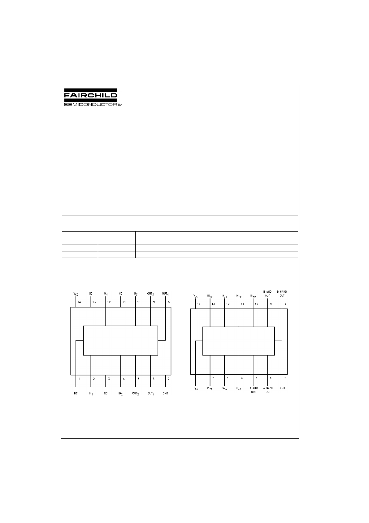
Connection Diagrams
Pin Assignments for DIP
MM88C29
Top View
Pin Assignments for DIP and SOIC
MM88C30
Top V iew
Order Number Package Number Package Description
MM88C29N N14A 14-Lead Plastic Dual-In-Line Package (PDIP), JEDEC MS-001, 0.300” Wide
MM88C30M M14A 14-Lead Small Outline Integrated Circuit (SOIC), JEDEC MS-120, 0.150” Narrow
MM88C30N N14A 14-Lead Plastic Dual-In-Line Package (PDIP), JEDEC MS-001, 0.300” Wide

www.fairchildsemi.com 2
MM88C29 • MM88C30
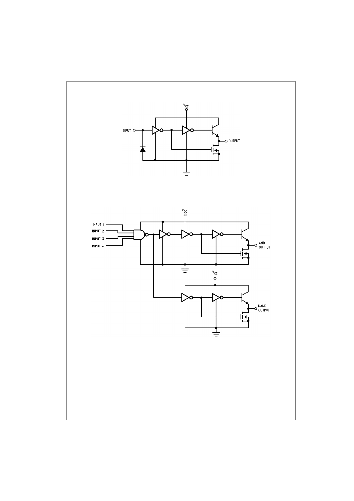
Logic Diagrams
1/4 MM88C29
1/2 MM88C30

3 www.fairchildsemi.com
MM88C29 • MM88C30
Absolute Maximum Ratings(Note 1)
Note 1: “Absolute Maximum Rat ings” are tho se values beyond which the
safety of the device cannot be guaranteed. Ex c ept for “ Operating Temperature Range” they are not mea nt to imply that the devices sh ould be operated at these limits. The Electrical Charact eristics tables provide c onditions
for actual device operation.
Note 2: AC Parameters are guaranteed by DC correlat ed testing.
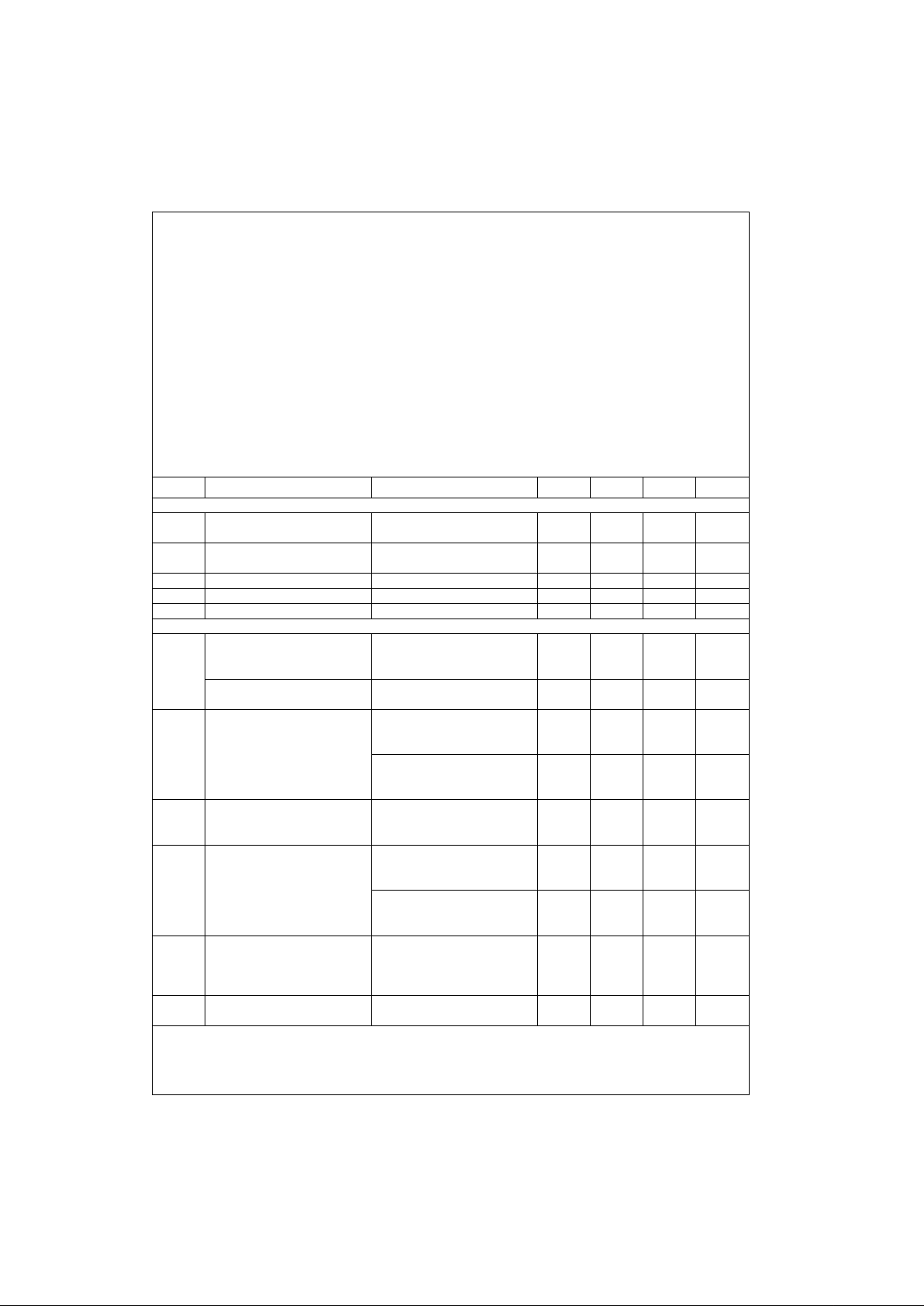
DC Electrical Characteristics
Min/Max limits apply across temperature range unless otherwise noted
Voltage at Any Pin (Note 2) −0.3V to VCC +16V
Operating Temperature Range −40°C to +85°C
Storage Temperature −65°C to +150°C
Power Dissipation (P
D
)
Dual-In-Line 700 mW
Small Outline 500 mW
Operating V
CC
Range 3V to 15V
Absolute Maximum V
CC
18V
Average Current at Output
MM88C30 50 mA
MM88C29 25 mA
Maximum Junction Temperature, T
j
150°C
Lead Temperature
(Soldering, 10 seconds) 260°C
Symbol Parameter Conditions Min Typ Max Units
CMOS TO CMOS
V
IN(1)
Logical “1” Input Voltage VCC = 5V 3.5 V
VCC = 10V 8 V
V
IN(0)
Logical “0” Input Voltage VCC = 5V 1.5 V
VCC = 10V 2 V
I
IN(1)
Logical “1” Input Current VCC = 15V, VIN = 15V 0.005 1 µA
I
IN(0)
Logical “0” Input Current VCC = 15V, VIN = 0V −1 −0.005 µA
I
CC
Supply Current VCC = 5V 0.05 100 mA
OUTPUT DRIVE
I
SOURCE
Output Source Current V
OUT
= VCC − 1.6V,
VCC ≥ 4.75V, Tj = 25°C −47 −80 mA
Tj = 85°C −32 −60 mA
MM88C29 V
OUT
= VCC − 0.8V −2 −20 mA
MM88C30 VCC ≥ 4.5V
I
SINK
Output Sink Current V
OUT
= 0.4V, VCC = 4.75V,
Tj = 25°C9.522mA
Tj = 85°C818mA
V
OUT
= 0.4V, VCC = 10V,
Tj = 25°C1940mA
Tj = 125°C 15.5 33 mA
I
SOURCE
Output Source Resistance V
OUT
= VCC − 1.6V,
VCC ≥ 4.75V, Tj = 25°C2034Ω
Tj = 85°C2750Ω
I
SINK
Output Sink Resistance V
OUT
= 0.4V, VCC = 4.75V,
Tj = 25°C1841Ω
Tj = 85°C2250Ω
V
OUT
= 0.4V, VCC = 10V,
Tj = 25°C1021Ω
Tj = 85°C1226Ω
Output Resistance
Temperature Coefficient
Source 0.55 %/°C
Sink 0.40 %/°C
θ
JA
Thermal Resistance 150 °C/W
(N-Package)
 Loading...