Fairchild Semiconductor KA555ID, KA555I, KA555D, KA555 Datasheet

©2002 Fairchild Semiconductor Corporation
www.fairchildsemi.com
Rev. 1.0.2
Features
• High Current Drive Capability (200mA)
• Adjustable Duty Cycle
• Temperature Stability of 0.005%/°C
• Timing From Msec to Hours
• Turn Off Time Less Than 2Msec
Applications
• Precision Timing
• Pulse Generation
• Time Delay Generation
• Sequential Timing
Description
The KA555 is a highly stable controller capable of
producing accurate timing pulses. With monos table
operation, the time delay is controlled by one external
resistor and one capacitor. With astable operation, the
frequency and duty cycle are accurately controlled with two
external resistors and one capacitor.
8-DIP
8-SOP
1
1
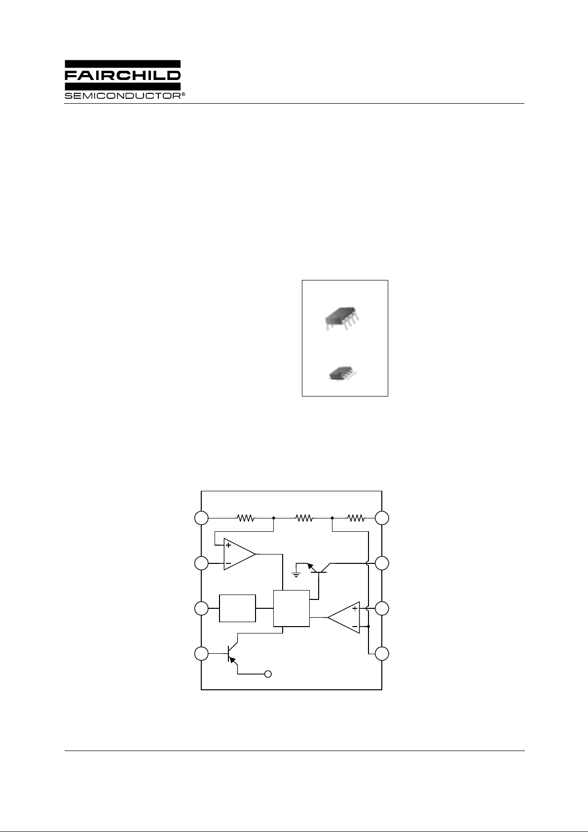
Internal Block Diagram
F/F
OutPut
Stage
1
7
5
2
3
4
6
8
RRR
Comp.
Comp.
Discharging Tr.
Vref
Vcc
Discharge
Threshold
Control
Voltage
GND
Trigger
Output
Reset
KA555
Single Timer

KA555
2
Absolute Maximum Ratings (T
A
= 25°°°°C)
Parameter Symbol Value Unit
Supply Voltage V
CC
16 V
Lead Temperature (Soldering 10sec) T
LEAD
300 °C
Power Dissipation P
D
600 mW
Operating Temperature Range
KA555/KA555I
T
OPR
0 ~ +70 / -40 ~ +85 °C
Storage Temperature Range T
STG
- 65 ~ +150 °C

KA555
3
Electrical Characteristics
(TA = 25°C, V
CC
= 5 ~ 15V, unless otherwise specified)
Notes:
1. Supply current when output is high is typically 1mA less at V
CC
= 5V
2. Tested at V
CC
= 5.0V and V
CC
= 15V
3. This will determin e maximum v alue of R
A
+ RB for 15V operation , the max . total R = 20MΩ, and for 5V op eratio n the ma x. total
R = 6.7MΩ
Parameter Symbol Conditions Min. Typ. Max. Unit
Supply Voltage V
CC
-4.5-16V
Supply Current *
1
(Low Stable) I
CC
VCC = 5V, RL = ∞ -36 mA
V
CC
= 15V, RL = ∞ -7.515 mA
Timing Error *
2
(Monos Table)
Initial Accuracy
Drift with Temperature
Drift with Supply Voltage
ACCUR
∆t/∆T
∆t/∆V
CC
RA = 1KΩ to100KΩ
C = 0.1µF
-1.0
50
0.1
3.0
0.5
%
ppm/°C
%/V
Timing Error *
2
(Astable)
Initial Accuracy
Drift with Temperature
Drift with Supply Voltage
ACCUR
∆t/∆T
∆t/∆V
CC
RA = 1KΩ to 100KΩ
C = 0.1µF
-
2.25
150
0.3
-%
ppm/°C
%/V
Control Voltage V
CC
VCC = 15V 9.0 10.0 11.0 V
V
CC
= 5V 2.6 3.33 4.0 V
Threshold Voltage V
TH
VCC = 15 V - 10.0 - V
V
CC
= 5V - 3.33 - V
Threshold Current *
3
I
TH
- - 0.1 0.25 µA
Trigger Voltage
V
TR
V
CC
= 5V 1.1 1.67 2.2 V
V
CC
= 15V 4.5 5 5.6 V
Trigger Current I
TR
V
TR
= 0V 0.01 2.0 µA
Reset Voltage V
RST
- 0.4 0.7 1.0 V
Reset Current I
RST
- 0.1 0.4 mA
Low Output Voltage V
OL
VCC = 15V
I
SINK
= 10mA
I
SINK
= 50mA
-0.06
0.3
0.25
0.75
V
V
V
CC
= 5V
I
SINK
= 5mA
-
0.05 0.35 V
High Output Voltage V
OH
VCC = 15V
I
SOURCE
= 200mA
I
SOURCE
= 100mA 12.75
12.5
13.3
-V
V
V
CC
= 5V
I
SOURCE
= 100mA 2.75 3.3
-
V
Rise Time of Output t
R
- - 100 - ns
Fall Time of Output t
F
- - 100 - ns
Discharge Leakage Current I
LKG
- - 20 100 nA

KA555
4
Application Information
Table1 below is the basic operating table of 555 timer:
When the low signal input is applied to the reset terminal, the timer output remains low regardless of the threshold voltage or
the trigger voltage. Only when the high signal is applied to the reset terminal, timer's output changes according to threshold
voltage and trigger voltage.
When the threshold voltage exceeds 2/3 of the supply voltage while the timer output is high, the timer's internal discharge Tr.
turns on, lowering the threshold voltage to below 1/3 of the supply voltage. During this time, the timer output is maintained
low. Later, if a low signal is applied to the trigger voltage so that it becomes 1/3 of the supply voltage, the timer's internal
discharge Tr. turns off, increasing the threshold voltage and driving the timer output again at high.
1. Monos Table Operation
Table 1. Basic Operating Table
Threshold Voltage
(V
th
)(Pin6)
Trigger Voltage
(Vtr)(Pin2)
Reset(Pin4) Output(Pin3)
Discharging Tr.
(Pin7)
Don't care Don't care Low Low ON
V
th
> 2Vcc / 3 Vth > 2Vcc / 3 High Low ON
Vcc / 3 < V
th
< 2 Vcc / 3 Vcc / 3 < Vth < 2 Vcc / 3 High - -
V
th
< Vcc / 3 Vth < Vcc / 3 High High OFF
10-510-410-310-210-110010110
2
10
-3
10
-2
10
-1
10
0
10
1
10
2
10M
Ω
ΩΩ
Ω
1M
Ω
ΩΩ
Ω
10k
Ω
ΩΩ
Ω
100k
Ω
ΩΩ
Ω
R
A
=1k
Ω
ΩΩ
Ω
Capacitance(uF)
Time Delay(s)
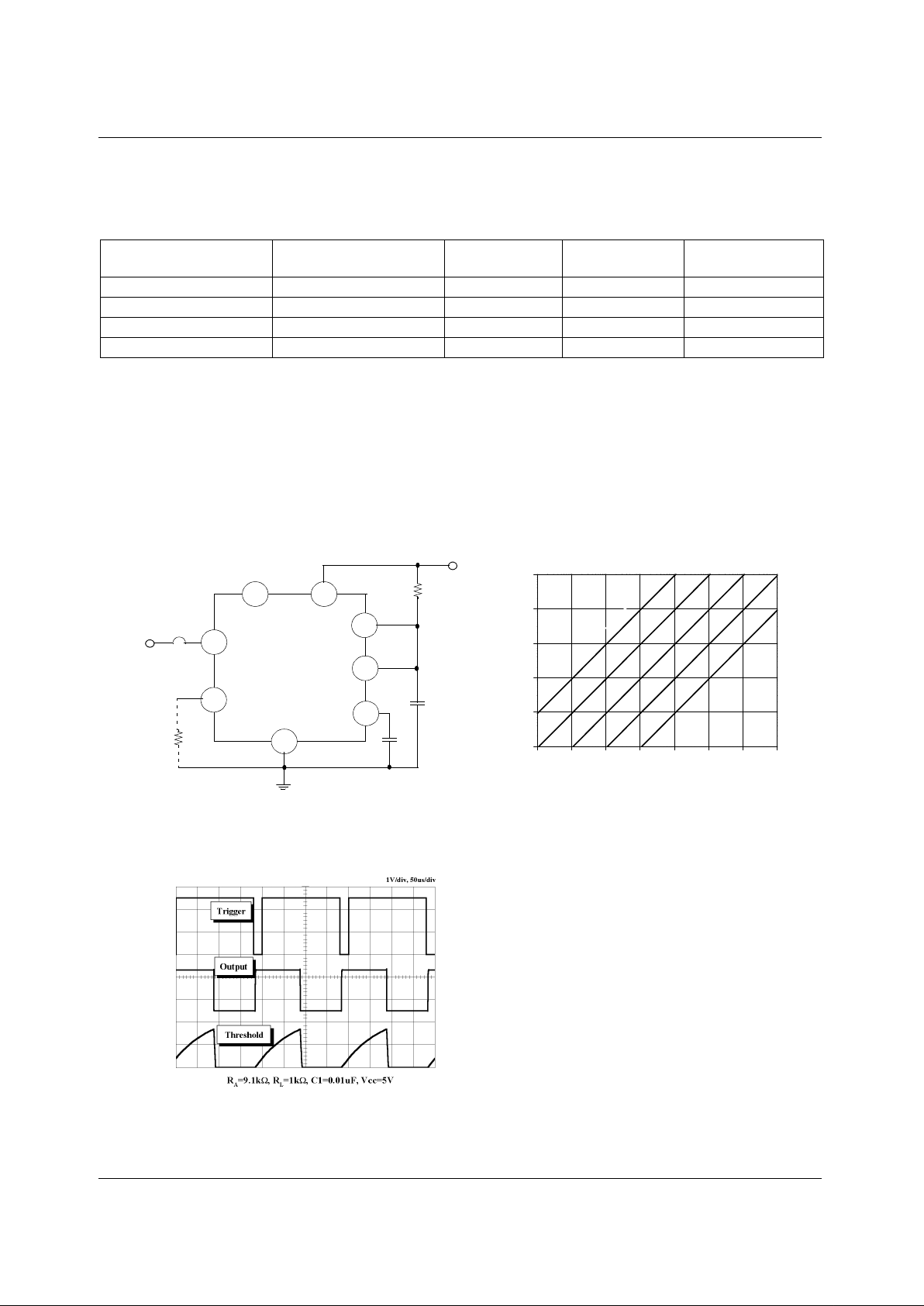
Figure 1. Monoatable Circuit
Figure 2. Resistance and Capacitance vs.
Time delay(td)
Figure 3. Waveform s of Monostable Operation
1
5
6
7
8
4
2
3
RESET
Vcc
DISCH
THRES
CONT
GND
OUT
TRIG
+Vcc
R
A
C1
C2R
L
Trigger

KA555
5
Figure 1 illustrates a monos table circuit. In this mode, the timer generates a fixed pulse whenever the trigger voltage falls
below Vcc/3. When the trigger pulse voltage applied to the #2 pin falls below Vcc/3 while the timer output is low, the timer's
internal flip-flop turns the discharging Tr. off and causes the timer output to become high by charging the external capacitor
C1and setting the flip-flop output at the same time.
The voltage across the external capacitor C1, V
C1
increases exponentially with the time constant t=RA*C and reaches 2Vcc/3
at td=1.1R
A
*C. Hence, capacitor C1 is charged through resistor RA. The greater the time constant RAC, the longer it takes
for the V
C1
to reach 2Vcc/3. In other words, the time constant RAC controls the output pulse width.
When the applied voltage to the capacitor C1 reaches 2Vcc/3, the comparator on the trigger terminal resets the flip-flop,
turning the discharging Tr. on. At this time, C1 begins to discharge and the timer output converts to low.
In this way, the timer operating in monos table repeats the above process. Figure 2 shows the time constant relationship based
on R
A
and C. Figure 3 shows the general waveforms during monos table operation.
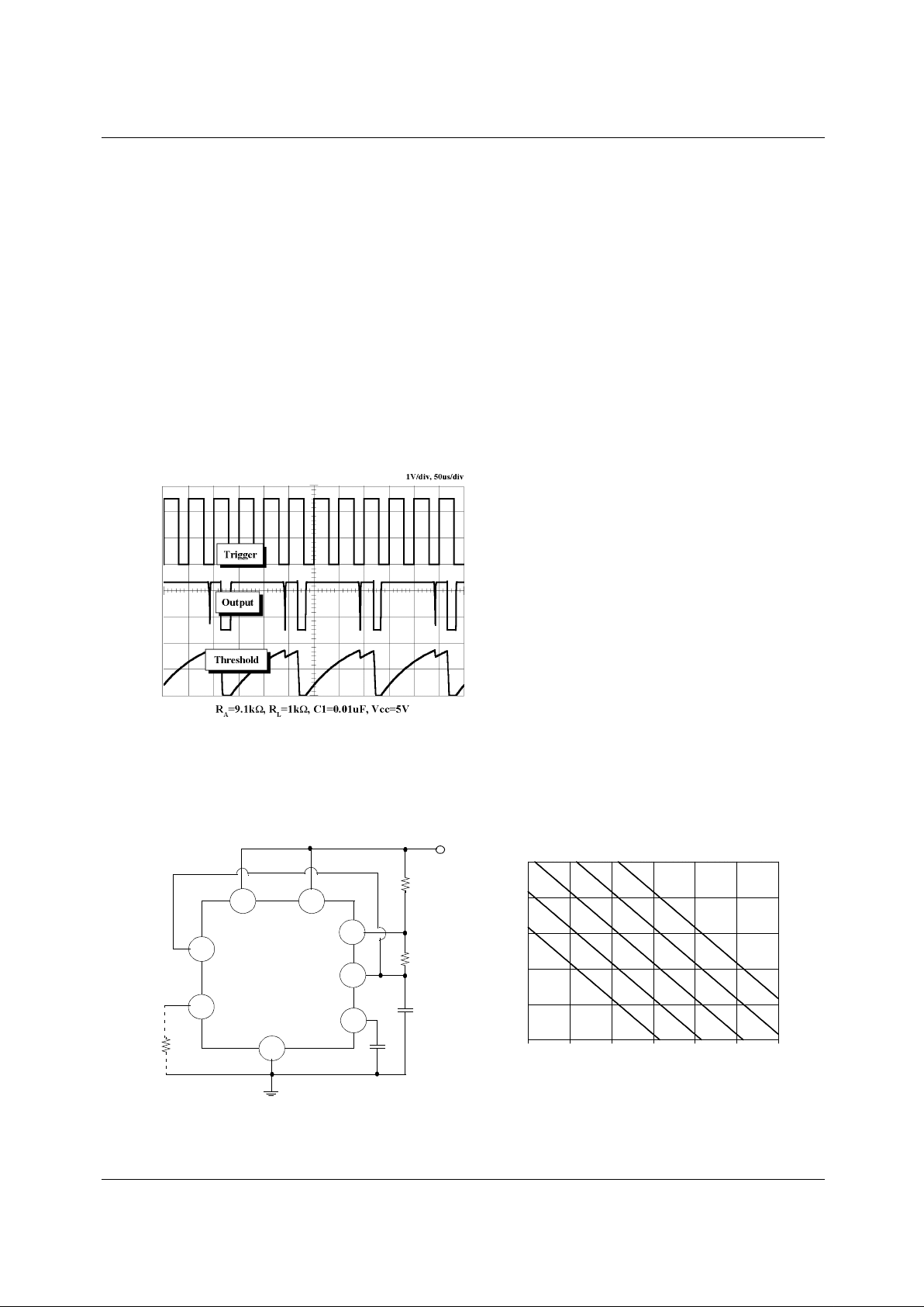
It must be noted that, for normal operation, the trigger pulse voltage needs to maintain a minimum of Vcc/3 before the timer
output turns low. That is, alth ough the output remains unaffected even if a different trigger pulse is applied while the output is
high, it may be affected and the waveform not operate properly if the trigger pulse voltage at the end of the output pulse
remains at below Vcc/3. Figure 4 shows such timer output abnormality.
2. Astable Operation
Figure 4. Waveforms of Monos table Operat ion (abnormal)
100m 1 10 100 1k 10k 100k
1E-3
0.01
0.1
1
10
100
10M
Ω
ΩΩ
Ω
1M
Ω
ΩΩ
Ω
100k
Ω
ΩΩ
Ω
10k
Ω
ΩΩ
Ω
1k
Ω
ΩΩ
Ω
(RA+2RB)
Capacitance(uF)
Frequency(Hz)
Figure 5. Astable Ci rcu it
Figure 6. Capac itance and Resist ance vs. Frequency
1
5
6
7
8
4
2
3
RESET
Vcc
DISCH
THRES
CONT
GND
OUT
TRIG
+Vcc
R
A
C1
C2R
L
R
B
 Loading...