

Fairchild Semiconductor H21A6, H21A5, H21A4 Datasheet
+
E+
D
2
0.129 (3.3)
0.119 (3.0)
0.433 (11.0)
0.422 (10.7)
0.315 (8.0)
0.110 (2.8)
0.091 (2.3)
1
3
4
0.020 (0.51) (SQ)
0.472 (12.0)
0.457 (11.6)
0.249 (6.35)
0.243 (6.15)
0.39 (1.00)
0.34 (0.85)
0.103 (2.60) NOM
0.125 (3.2)
0.119 (3.0)
Ø 0.133 (3.4)
Ø 0.126 (3.2)
(2X)
0.755 (19.2)
0.745 (18.9)
L
C
C
L
L
C
Optical
C
L
0.972 (24.7)
0.957 (24.3)
.295 (7.5)
.272 (6.9)
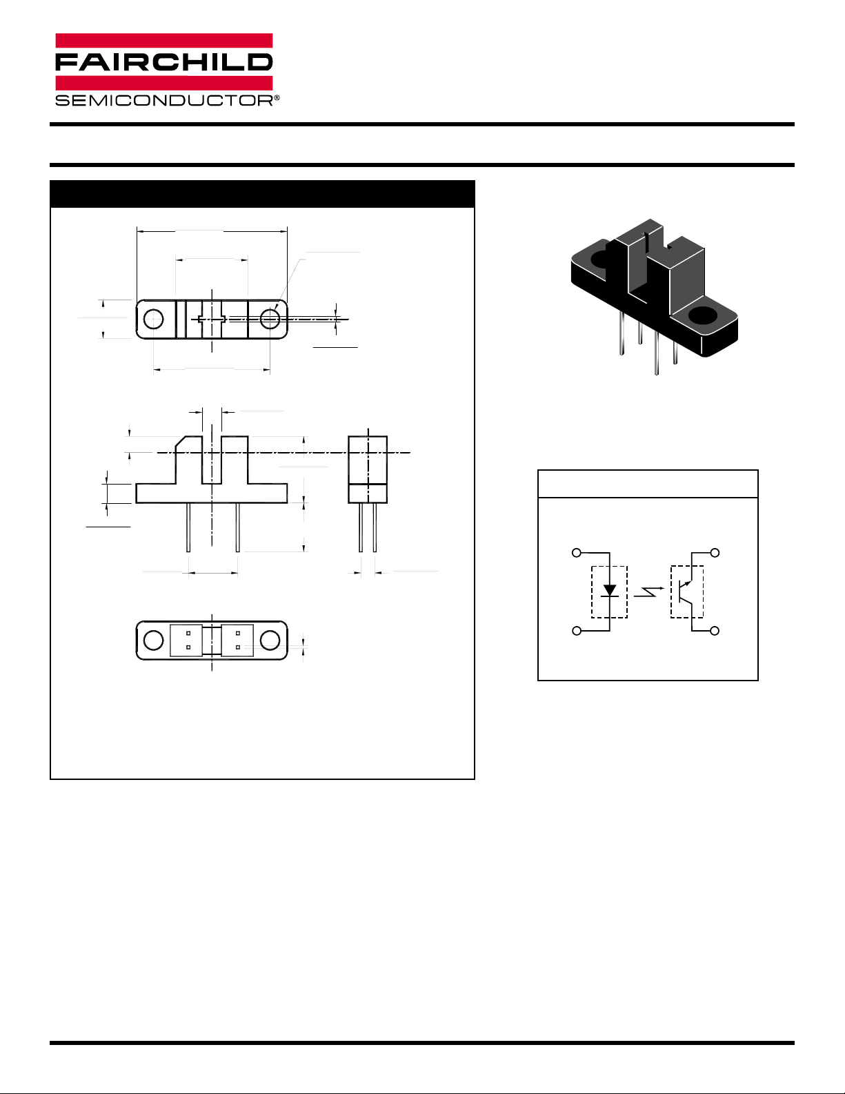
PIN 1 ANODE
PIN 2 CATHODE
PIN 3 COLLECTOR
PIN 4 EMITTER
PACKAGE DIMENSIONS
FEATURES
• Opaque housing
• Low cost
• .035” apertures
• High I
C(ON)
NOTES:
1. Dimensions for all drawings are in inches (mm).
2. Tolerance of ± .010 (.25) on all non-nominal dimensions
unless otherwise specified.
PHOTOTRANSISTOR
OPTICAL INTERRUPTER SWITCH
DESCRIPTION
The H21A series are gallium arsenide infrared emitting diode coupled with a silicon photodarlington in a plastic housing. The
packaging system is designed to optimize the mechanical resolution, coupling efficiency, ambient light rejection, cost and
reliability. The gap in the housing provides a means of interrupting the signal with an opaque material, switching the output
from an “ON” to an “OFF” state.
SCHEMATIC
2001 Fairchild Semiconductor Corporation
DS300291 6/05/01 1 OF 4 www.fairchildsemi.com
H21A4 H21A5 H21A6
1
2
4
3
www.fairchildsemi.com 2 OF 4 6/05/01 DS300291
PARAMETER TEST CONDITIONS SYMBOL DEVICES MIN TYP MAX UNITS
INPUT (EMITTER)
Forward Voltage
I
F
= 60 mA V
F
All — — 1.7 V
Reverse Breakdown Voltage IR= 10 µAV
R
All
6.0 — — µA
Reverse Leakage Current VR= 3 V I
R
All
— — 1.0 µA
OUTPUT (SENSOR)
Emitter to Collector Breakdown
I
F
= 100 µA, Ee = 0 BV
ECO
All 6.0 — — V
Collector to Emitter Breakdown IC= 1 mA, Ee = 0 BV
CEO
All
55 — — V
Collector to Emitter Leakage VCE= 45 V, Ee = 0 I
CEO
All
— — 100 nA
COUPLED
H21A4
0.15 — —
I
F
= 5 mA, VCE= 5 V
H21A5 0.30
——
H21A6 0.60
——
H21A4
1.0 — —
On-State Collector Current I
F
= 20 mA, VCE= 5 V I
C(ON)
H21A5
2.0 — — mA
H21A6
4.0 — —
H21A4
1.9 — —
I
F
= 30 mA, VCE= 5 V
H21A5
3.0 — —
H21A6
5.5 — —
Saturation Voltage
I
F
= 20 mA, IC= 1.8 mA
V
CE(SAT)
H21A5/6 — — 0.40 V
I
F
= 30 mA, IC= 1.8 mA H21A4 — — 0.40 V
Turn-On Time
IF= 30 mA, VCC= 5 V, RL= 2.5 KΩ
t
on
All
—8 —µs
Turn-Off Time
IF= 30 mA, VCC= 5 V, RL= 2.5 KΩ
t
off
All
—50 —µs
ELECTRICAL / OPTICAL CHARACTERISTICS
(TA =25°C) (All measurements made under pulse conditions)
Parameter Symbol Rating Unit
Operating Temperature T
OPR
-55 to +100 °C
Storage Temperature T
STG
-55 to +100 °C
Soldering Temperature (Iron)
(2,3 and 4)
T
SOL-I
240 for 5 sec °C
Soldering Temperature (Flow)
(2 and 3)
T
SOL-F
260 for 10 sec °C
INPUT (EMITTER)
Continuous Forward Current
I
F
50 mA
Reverse Voltage V
R
6V
Power Dissipation
(1)
P
D
100 mW
OUTPUT (SENSOR)
Collector to Emitter Voltage
V
CEO
55 V
Emitter to Collector Voltage V
ECO
4.5 V
Collector Current I
C
20 mA
Power Dissipation(TC= 25°C)
(1)
P
D
150 mW
ABSOLUTE MAXIMUM RATINGS
(TA= 25°C unless otherwise specified)
NOTE:
1. Derate power dissipation linearly 1.67 mW/°C above 25°C.
2. RMA flux is recommended.
3. Methanol or isopropyl alcohols are recommended as cleaning agents.
4. Soldering iron tip
1/16” (1.6mm) minimum from housing.
PHOTOTRANSISTOR
OPTICAL INTERRUPTER SWITCH
H21A4 H21A5 H21A6
 Loading...