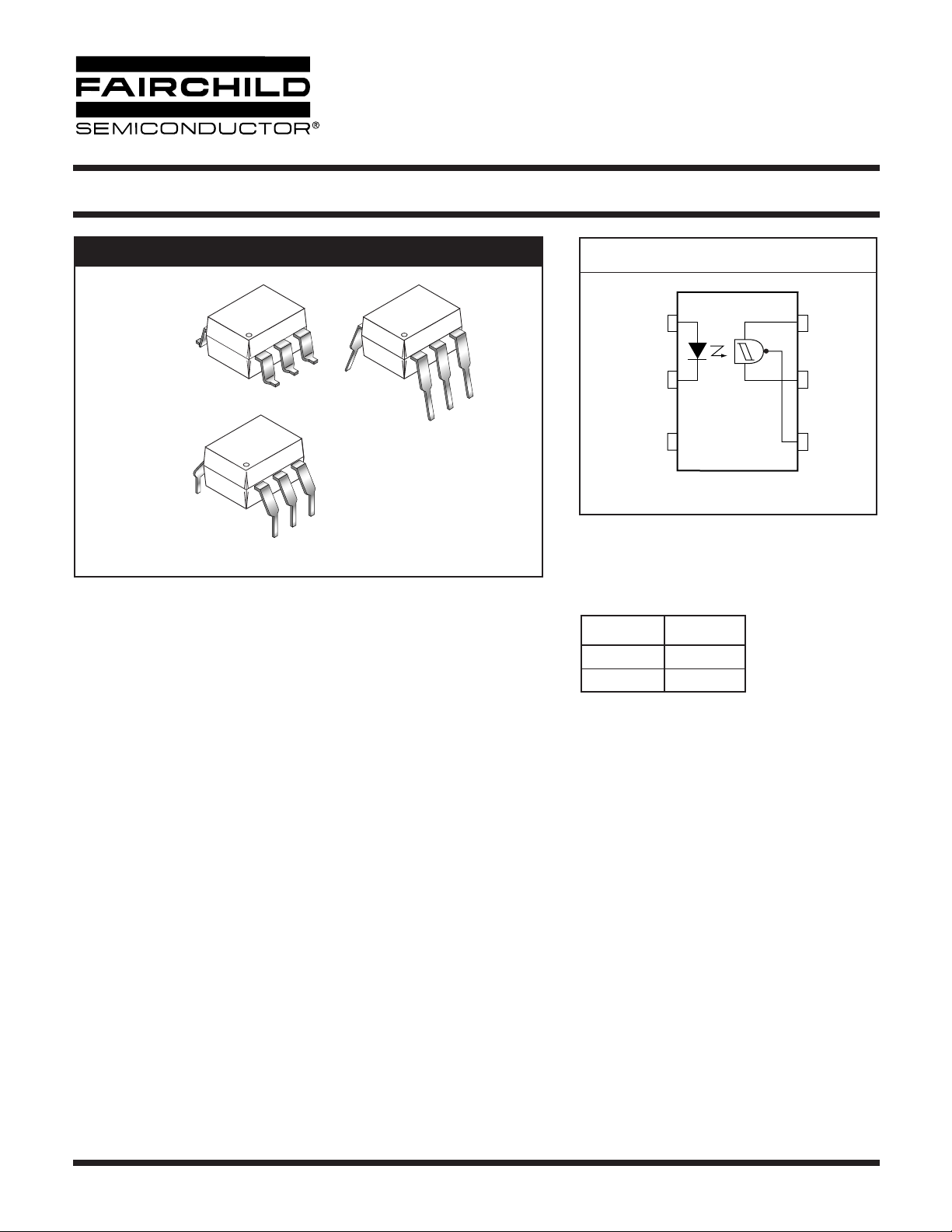
6-PIN DIP
HIGH SPEED LOGIC OPTOCOUPLERS
H11N1-M H11N2-M H11N3-M
PACKAGE
6
6
1
1
6
1
DESCRIPTION
The H11NX-M series has a high speed integrated circuit detector optically
coupled to an AlGaAs infrared emitting diode. The output incorporates a
Schmitt trigger, which provides hysteresis for noise immunity and pulse s
haping. The detector circuit is optimized for simplicity of operation and utilizes
an open collector output for maximum application flexibility.
SCHEMATIC
1
ANODE
CATHODE
2
3
Truth Table
Input Output
HL
LH
V
6
CC
5GND
V
4
O
FEATURES
• High data rate, 5 MHz typical (NRZ)
•Free from latch up and oscilliation throughout voltage and temperature ranges.
• Microprocessor compatible drive
• Logic compatible output sinks 16 mA at 0.5 V maximum
• Guaranteed on/off threshold hysteresis
• Wide supply voltage capability, compatible with all popular logic systems
• High common mode transient immunity, 2000 V/µs minimum
•Fast switching t
• Underwriter Laboratory (UL) recognized—file #E90700
• VDE recognized – File#102497 – Add option V (e.g., H11N1VM)
= 7.5ns typical, t
r
= 12ns typical
f
APPLICATIONS
• Logic to logic isolator
• Programmable current level sensor
• Line receiver—eliminate noise and transient problems
• A.C. to TTL conversion—square wave shaping
• Interfaces computers with peripherals
• Isolated power MOS driver for power supplies
© 2003 Fairchild Semiconductor Corporation
Page 1 of 9
4/14/03

6-PIN DIP
HIGH SPEED LOGIC OPTOCOUPLERS
H11N1-M H11N2-M H11N3-M
ABSOLUTE MAXIMUM RATINGS
Parameters Symbol Device Value Units
TOTAL DEVICE
Storage Temperature
Operating Temperature
Lead Solder Temperature
Total Device Power Dissipation @ 25°C
Derate Above 25°C 2.94 mW/°C
EMITTER
Continuous Forward Current
Reverse Voltage
Forward Current - Peak (1 µs pulse, 300 pps)
LED Power Dissipation 25°C Ambient
Derate Linearly From 25°C 1.41 mW/°C
DETECTOR
Detector Power Dissipation @ 25°C
Derate Linearly from 25°C 1.76 mW/°C
Allowed Range V
V
45
V
Allowed Range V
65
I
Output Current I
4
T
T
T
I
P
V
F
P
P
STG
OPR
SOL
D
I
F
R
(pk)
D
D
O
CC
O
All -55 to +150 °C
All -40 to +85 °C
All 260 for 10 sec °C
All
250 mW
All 30 mA
All 6 V
All 1.0 A
All
All
120 mW
150 mW
All 0 to 16 V
All 0 to 16 V
All 50 mA
ELECTRICAL CHARACTERISTICS
(T
= 0-70°C Unless otherwise specified.)
A
INDIVIDUAL COMPONENT CHARACTERISTICS
Parameters Test Conditions Symbol Device Min Typ* Max Units
EMITTER
= 10 mA
I
Input Forward Voltage
Reverse Current
F
I
= 0.3 mA
F
V
= 5 V I
R
Capacitance V = 0, f = 1.0 MHz
DETECTOR
Operating Voltage Range
I
Supply Current
Output Current, High
*Typical values at T
© 2003 Fairchild Semiconductor Corporation
= 25°C
A
= 0, V
F
I
= 0.3mA, V
F
= 5V I
CC
CC
= V
O
= 15V I
Page 2 of 9
V
F
R
C
J
V
CC
CC(off)
OH
All
0.75 1.25
All 10 µA
All 100 pF
All 4 15 V
All 6 10 mA
All 100 µA
1.4 2
4/14/03
V

6-PIN DIP
HIGH SPEED LOGIC OPTOCOUPLERS
H11N1-M H11N2-M H11N3-M
TRANSFER CHARACTERISTICS
DC Characteristics Test Conditions Symbol Device Min Typ* Max Units
I
Supply Current
Output Voltage, low
Tu r n-On Threshold Current
Tu r n-Off Threshold Current
Hysteresis Ratio
= 10mA, V
F
R
=270 Ω ,V
L
R
=270 Ω , V
L
note 1
R
=270 Ω , V
L
R
=270 Ω , V
L
AC Characteristics Test Conditions Symbol Device Min Typ Max Units
= 5V I
CC
=5V, I
=I
CC
CC
CC
CC
F
= 5V
= 5V I
= 5V I
max. V
F(on)
CC(on)
I
F(off)
OL
F(on)
F(off)
/I
All 6.5 10 mA
All 0.5 V
H11N1-M 0.8 3.2
H11N3-M 4.1 10
All 0.3 mA
F(on)
All 0.65 0.95
mAH11N2-M 2.3 5
SWITCHING SPEED
Propagation delay time
High to Low
Rise Time
Propagation delay time
Low to High
Fall time
C=120pF, t
Fig. 1
C=120pF, t
Fig. 1
C=120pF, t
Fig. 1
C=120pF, t
Fig. 1
=1µs, R
P
=1µs, R
P
=1µs, R
P
=1µs, R
P
: Note 2
E
: Note 2
E
: Note 2
E
: Note 2
E
t
PHL
t
PLH
All 100 330 ns
t
r
All 7.5 ns
All 150 330 ns
t
f
All 12 ns
Data Rate All 5 MHz
ISOLATION CHARACTERISTICS
Parameters Test Conditions Symbol Min Typ* Max Units
Input-Output Isolation Voltage f = 60 Hz, t =1 sec.
V
Isolation Capacitance
Isolation Resistance
*Typical values at T
= 25°C
A
= 0V, f = 1 MHz C
I-O
V
= ±500 VDC R
I-O
V
ISO
ISO
ISO
7500
11
10
0.4 0.6 pF
NOTES:
1. Maximum I
is the maximum current required to trigger the output. For example, a 3.2mA maximum trigger current would
F(ON)
require the LED to be driven at a current greater than 3.2mA to guarantee the device will turn on. A 10% guard band is
recommended to account for degradation of the LED over its lifetime. The maximum allowable LED drive current is 30mA.
2. H11N1: R
H11N2: R
H11N3: R
= 910 Ω
E
= 560 Ω
E
= 240 Ω
E
V
PEAK
Ω
© 2003 Fairchild Semiconductor Corporation
Page 3 of 9
4/14/03
 Loading...