

Fairchild Semiconductor GTLP6C817MTCX, GTLP6C817MTC Datasheet
© 1999 Fairchild Semiconductor Corporation DS500246 www.fairchildsemi.com
June 1999
Revised August 1999
GTLP6C817 Low Drive GTLP-to-LVTTL 1:6 Clock Driver
GTLP6C817
Low Drive GTLP-to-LVTTL 1:6 Clock Driver
General Description
The GTLP6C817 is a l ow drive clock driver tha t provides
TTL to GTLP signal lev el trans lation (and vice ver sa). The
device provides a high speed interface between cards
operating at TTL l ogic le vels and a backp lane o perat ing at
GTLP logic levels. H igh speed backplane operation is a
direct result of GTLP’s reduced output swing (<1V),
reduced input threshold leve ls and output edge rate control. The edge rate control minimizes bus settling time.
GTLP is a Fairchild Semiconduct or derivative of the Gunning Transceiver logic (GTL) JEDEC standard JESD8-3.
Fairchild’s GTLP has intern al edge -rate cont rol and is process, voltage, and temperature (PVT) compensated. Its
function is similar to BTL and GT L but with different outp ut
levels and receiver threshold. GTLP output LOW level is
typically less than 0. 5V, the output level HIGH is 1.5V and
the receiver threshold is 1.0V.
Features
■ Interface between TTL and GTLP logic levels
■ Edge Rate Control to minimize noise on the GTLP port
■ Power up/down high impedance for live insertion
■ 1:6 fanout clock driver for LVTTL port
■ 1:2 fanout clock driver for GTLP port
■ LVTTL compatible driver and control inputs
■ 5V over voltage tolerance on LVTTL ports
■ Flow through pinout optimizes PCB layout
■ Open drain on GTLP to support wired-or connection
■ Recommended Operating Temperature −40°C to +85°C
Ordering Code:
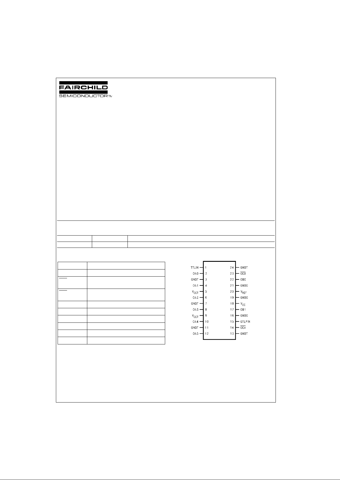
Pin Descriptions Connection Diagram
Order Number Package Number Package Description
GTLP6C817M TC MTC24 24-Lead Thin Shrink S m all Ou t li n e Pac ka ge ( TSSOP), JEDE C MO - 15 3 , 4. 4 mm W id e
Pin Names Description
TTLIN, GTLPIN Clock Inputs (TTL and GTLP respectively)
OEB
Output Enable (Active LOW)
GTLP Port (TTL Levels)
OEA
Output Enable (Active LOW)
TTL Port (TTL Levels)
V
CCT
.GNDT LVTTL Output Supplies (3V)
V
CC
Internal Circuitry VCC (5V)
GNDG OBn GTLP Output Grounds
V
REF
Voltage Reference Input
OA0–OA5 TTL Buffered Clock Outputs
OB0–OB1 GTLP Buffered Clock Outputs
www.fairchildsemi.com 2
GTLP6C817
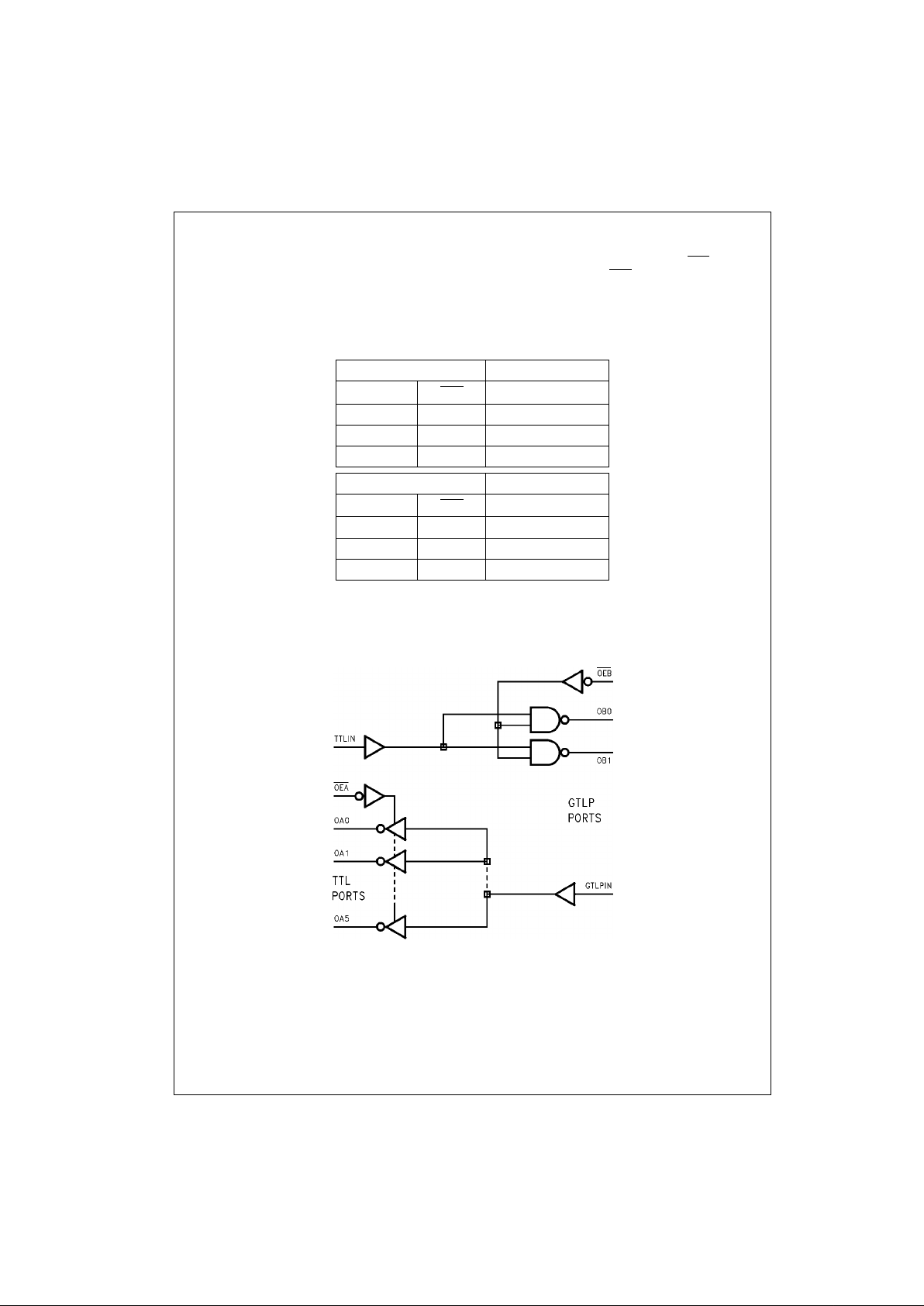
Functional Description
The GTLP6C817 is a low drive clock driver providing LVTTL-to-GTLP clock translation, and GTLP-to-LVTTL clock translation in the same packa ge. T he LVTTL-to-GTLP dire ction i s a 1:2 c lock dri ver pa th wit h a single Enab le pin (O EB
). For the
GTLP-to-LVTTL direction the clock receiver path is a 1:6 buffer with a single Enable control (OEA
). Data polarity is inverting
for both directions.
Truth Tables
Logic Diagram
Inputs Outputs
TTLIN OEB
OBn
HL L
LL H
X H High Z
Inputs Outputs
GTLPIN OEA
OAn
HL L
LL H
X H High Z

3 www.fairchildsemi.com
GTLP6C817
Absolute Maximum Ratings(Note 1) Recommended Operating
Conditions
(Note 3)
Note 1: Absolute Maximum continuous ratings are those values beyond
which damage t o the device ma y occur. Exposure to t hese condition s or
conditions beyon d those indicated m ay adversely affect dev ice reliability.
Functional operation under absolute maximum rated conditions is not
implied.
Note 2: I
o
Absolute Maximum Rating must be observed.
Note 3: Unused input must be held HIGH or LOW.
Supply Voltage (VCC) −0.5V to +7.0V
DC Input Voltage (V
I
) −0.5V to +7.0V
DC Output Voltage (V
O
)
Outputs 3-STATE −0.5V to +7.0V
Outputs Active (Note 2) −0.5V to +7.0V
DC Output Sink Current into
OA-Port I
OL
24 mA
DC Output Source Current
from OA-Port I
OH
−24 mA
DC Output Sink Current into
OB-Port in the LOW State I
OL
80 mA
DC Input Diode Current (I
IK
)
V
I
< 0V −50 mA
DC Output Diode Current (I
OK
)
V
O
< 0V −50 mA
V
O
> V
CC
+50 mA
ESD Rating > 2000V
Storage Temperature (T
STG
) −65°C to +150°C
Supply Voltage
V
CC
4.75V to 5.25V
V
CCT
3.15V to 3.45V
Bus Termination Voltage (V
TT
)
GTLP 1.47V to 1.53V
V
REF
0.98V to 1.02V
Input Voltage (V
I
) on INA-Port
and Control Pins 0.0V to 5.5V
HIGH Level Output Current (I
OH
)
OA-Port −12 mA
LOW Level Output Current (I
OL
)
OA-Port +12 mA
OB-Port +40 mA
Operating Temperature (T
A
) −40°C to +85°C
 Loading...