

Fairchild Semiconductor DM74LS253M, DM74LS253N, DM74LS253MX Datasheet
© 2000 Fairchild Semiconductor Corporation DS006416 www.fairchildsemi.com
August 1986
Revised March 2000
DM74LS253 3-STATE Data Selector/Multiplexer
DM74LS253
3-STATE Data Selector/Multiplexer
General Description
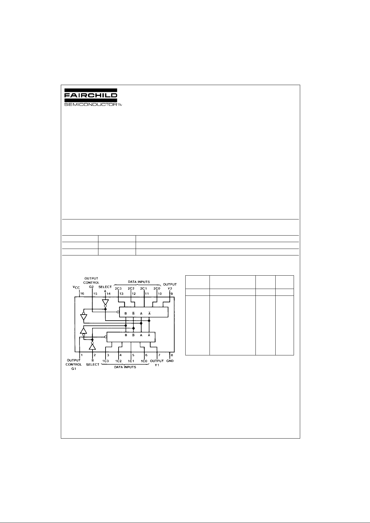
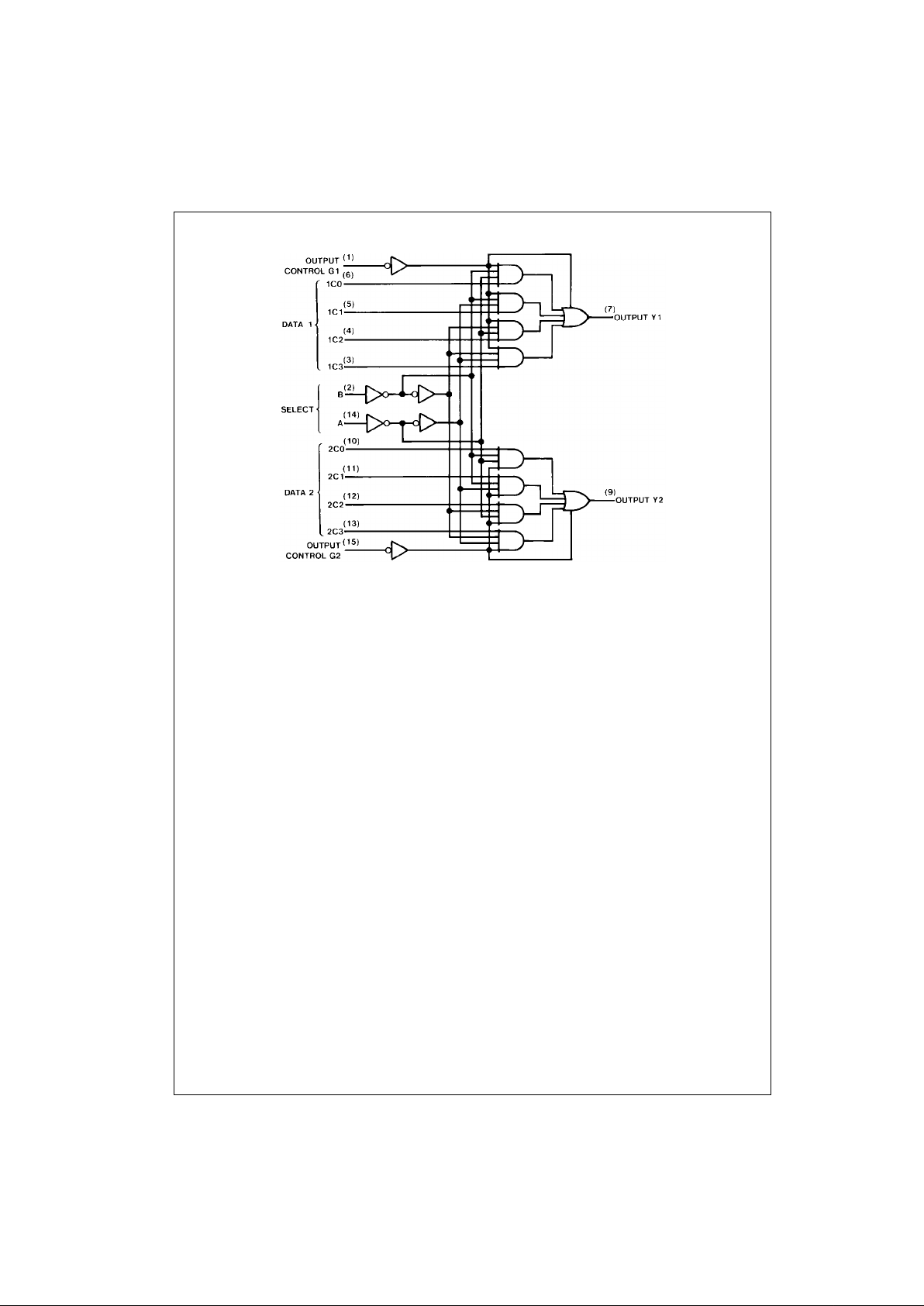
Each of these Schottky-clamped data selector s/multiplexers contains inverter s and drivers to supply ful ly complementary, on-chip, binary decoding data selection to the
AND-OR gates. Separate output control inputs are provided for each of the two four-line sections.
The 3-STATE outputs can interface di rectly with data l ines
of bus-organized syste ms. Wit h all but one of the co mmon
outputs disabled (at a high impedance state), the low
impedance of the single enabled output will drive the bus
line to a HIGH or LOW logic level.
Features
■ 3-STATE version of DM74LS153 with same pinout
■ Schottky-diode-clamp ed tra nsisto rs
■ Permit multiplexing from N-lines to one line
■ Performs parallel-to-serial con version
■ Strobe/output control
■ High fanout totem-pole outputs
■ Typical propagation delay
Data to output 12 ns
Select to output 21 ns
■ Typical power di ssipation 35 mW
Ordering Code:
Devices also availab le in Tape and Reel. Specify by appending th e s uffix let t er “X” to the ordering code.
Connection Diagram Function Table
Address Inputs A and B are common to both sections.
H = HIGH Level
L = LOW Level
X = Don't Care
Z = High Impedance (OF F )
Order Number Package Number Package Description
DM74LS253M M16A 16-Lead Small Outline Integrated Circuit (SOIC), JEDEC MS-0 12, 0.150 Narrow
DM74LS253N N16E 16-Lead Plastic Dual-In-Line Package (PDIP), JEDEC MS-001, 0.300 Wide
Select Data Inputs Output Output
Inputs Control
B A C0 C1 C2 C3 G Y
XXXXXX H Z
LLLXXX L L
LLHXXX L H
LHXLXX L L
LHXHXX L H
HLXXLX L L
HLXXHX L H
HHXXXL L L
HHXXXH L H
www.fairchildsemi.com 2
DM74LS253
Logic Diagram
 Loading...