Fairchild Semiconductor DM74LS245WMX, DM74LS245WM, DM74LS245SJX, DM74LS245SJ, DM74LS245N Datasheet
...
© 2000 Fairchild Semiconductor Corporation DS006413 www.fairchildsemi.com
August 1986
Revised March 2000
DM74LS245 3-STATE Octal Bus Transceiver
DM74LS245
3-STATE Octal Bus Transceiver
General Description
These octal bus transceivers ar e designed for asynchronous two-way communication between data buses. The
control function im plementation minimizes exte rnal timing
requirements.
The device allows data t ransmiss ion fr om the A Bus to t he
B Bus or from the B Bus to th e A Bus depe ndin g upo n the
logic level at the direction control (DIR) input. The enable
input (G
) can be used to disa ble the device so that the
buses are effectively isolated.
Features
■ Bi-Directional bus tr ansceiver in a high-density 20-pin
package
■ 3-STATE outputs drive bus lines directly
■ PNP inputs reduce DC loading on bus lines
■ Hysteresis at bus inputs improve noise margins
■ Typical propagation delay times, port-to-port 8 ns
■ Typical enable/disable times 17 ns
■ I
OL
(sink current)
24 mA
■ I
OH
(source current)
−15 mA
Ordering Code:
Devices also availab le in Tape and Reel. Specify by appending th e s uffix let t er “X” to the ordering code.
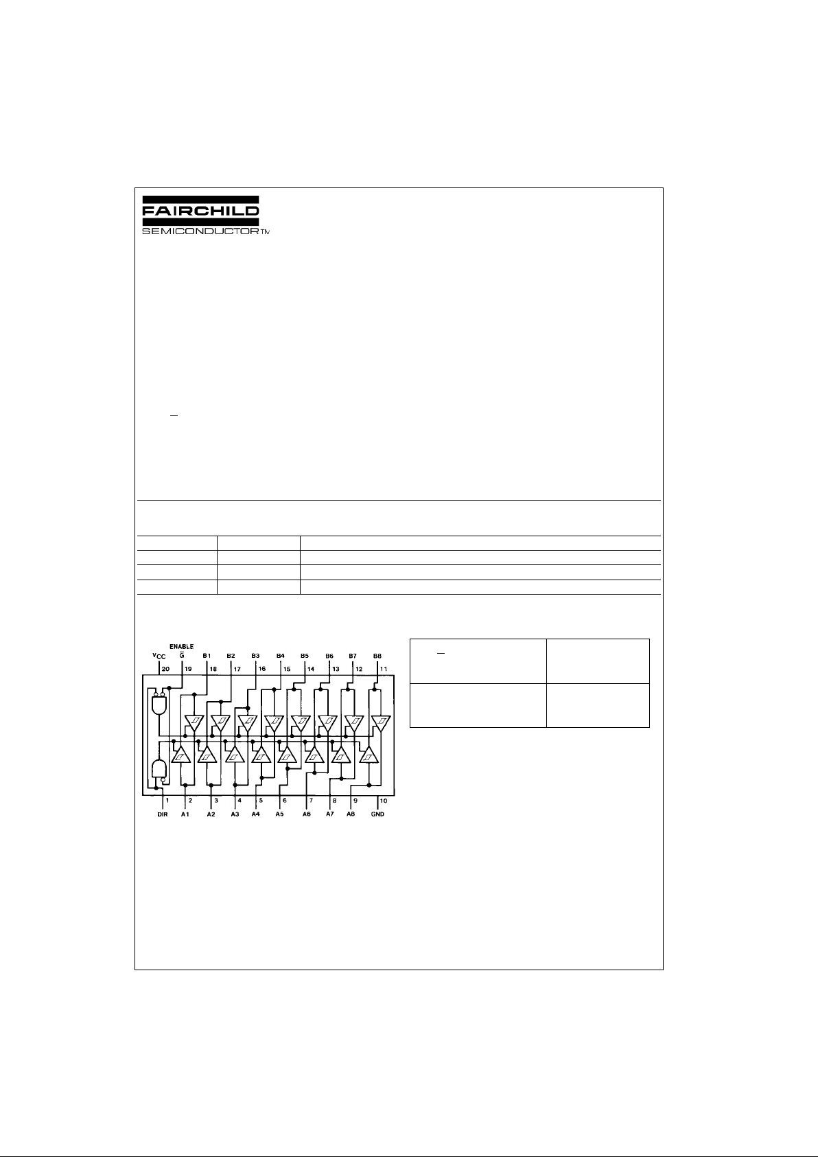
Connection Diagram Function Table
H = HIGH Level
L = LOW Level
X = Irrelevant
Order Number Package Number Package Description
DM74LS245WM M20B 20-Lead Small Outline Integrated Circuit (SOIC), JED EC MS-013, 0.300 Wide
DM74LS245SJ M20D 20-Lead Small Outline Package (SOP), EIAJ TYPE II, 5.3mm Wide
DM74LS245N N20A 20-Lead Plastic Dual-In-Line Package (PDIP), JEDEC MS-001, 0.300 Wide
Enable Direction Operation
G
Control
DIR
L L B Data to A Bus
L H A Data to B Bus
HX Isolation

www.fairchildsemi.com 2
DM74LS245
Absolute Maximum Ratings(Note 1)
Note 1: The “Absolute Maximum Ratings” are those values beyond which
the safety of the dev ice cannot be guaranteed. T he device sh ould not be
operated at these limits. The parametric values defined in the Electrical
Characteristics tables are not guaranteed at the absolute maximum ratings.
The “Recommend ed O peratin g Cond itions” t able w ill defin e the co ndition s
for actual device operation.
Recommended Operating Conditions
Electrical Characteristics
over recommended operating free air temperature range (unless otherwise noted)
Note 2: All typicals are at VCC = 5V, TA = 25°C.
Note 3: Not more than one output should be shorted at a time, not to exceed one second duration
Supply Voltage 7V
Input Voltage
DIR or G
7V
A or B 5.5V
Operating Free Air Temperature Range 0°C to +70°C
Storage Temperature Range −65°C to +150°C
Symbol Parameter Min Nom Max Units
V
CC
Supply Voltage 4.75 5 5.25 V
V
IH
HIGH Level Input Voltage 2 V
V
IL
LOW Level Input Volt age 0.8 V
I
OH
HIGH Level Output Current −15 mA
I
OL
LOW Level Output Current 24 mA
T
A
Free Air Operating Temperature 0 70 °C
Symbol Parameter Conditions Min
Typ
Max Units
(Note 2)
V
I
Input Clamp Voltage VCC = Min, II = −18 mA −1.5 V
HYS Hysteresis (VT+ − VT−)V
CC
= Min 0.2 0.4 V
V
OH
HIGH Level VCC = Min, VIH = Min
2.7
Output Voltage VIL = Max, IOH = −1 mA
VCC = Min, VIL = Min
2.4 3.4 V
VIL = Max, IOH = −3 mA
VCC = Min, VIH = Min
2
VIL = 0.5V, IOH = Max
V
OL
LOW Level VCC = Min IOL = 12 mA 0.4
Output Voltage VIL = Max
IOL = Max 0.5
V
VIH = Min
I
OZH
Off-State Output Current, VCC = Max
VO = 2.7V 20 µA
HIGH Level Voltage Applied VIL = Max
I
OZL
Off-State Output Current, VIH = Min
VO = 0.4V −200 µA
LOW Level Voltage Applied
I
I
Input Current at Maximum VCC = Max A or B VI = 5.5V 0.1
mA
Input Voltage DIR or G VI = 7V 0.1
I
IH
HIGH Level Input Current VCC = Max, VI = 2.7V 20 µA
I
IL
LOW Level Input Current VCC = Max, VI = 0.4V −0.2 mA
I
OS
Short Circuit Output Current VCC = Max (Note 3) −40 −225 mA
I
CC
Supply Current Outputs HIGH
VCC = Max
48 70
Outputs LOW 62 90 mA
Outputs at Hi-Z 64 95
 Loading...