© 2000 Fairchild Semiconductor Corporation DS005994 www.fairchildsemi.com
October 1987
Revised August 2000
CD4514BC• CD4515BC 4-Bit Latched/4-to-16 Line Decoders
CD4514BC• CD4515BC
4-Bit Latched/4-to-16 Line Decoders
General Description
The CD4514BC and CD45 15BC are 4 -to-16 lin e decoders
with latched inputs implemented with complementary MOS
(CMOS) circuits constructed with N- and P-channel
enhancement mode transistor s. These circuits are primarily used in decoding applications where low power dissipation and/or high noise immunity is required.
The CD4514BC (output a cti ve h igh op ti on ) pr ese nts a lo gi cal “1” at the selected output, whereas the CD4515BC presents a logical “0” at the selected output. Th e in put latches
are R–S type flip-flops, which hold the last input data presented prior to the strobe transition from “1” to “0”. This
input data is decoded and the corresponding output is ac tivated. An output inhibit line is also available.
Features
■ Wide supply voltage range: 3.0V to 15V
■ High noise immunity: 0.45 V
DD
(typ.)
■ Low power TTL: fan out of 2
compatibility: driving 74L
■ Low quiesc ent power dissipation:
0.025
µW/package @ 5.0 V
DC
■ Single supply operation
■ Input impedance
= 1012Ω typically
■ Plug-in replacement for MC14514, MC14515
Ordering Code:
Devices also available in Tape and Reel. Specify by appending suffix letter “X” to the ordering co de.
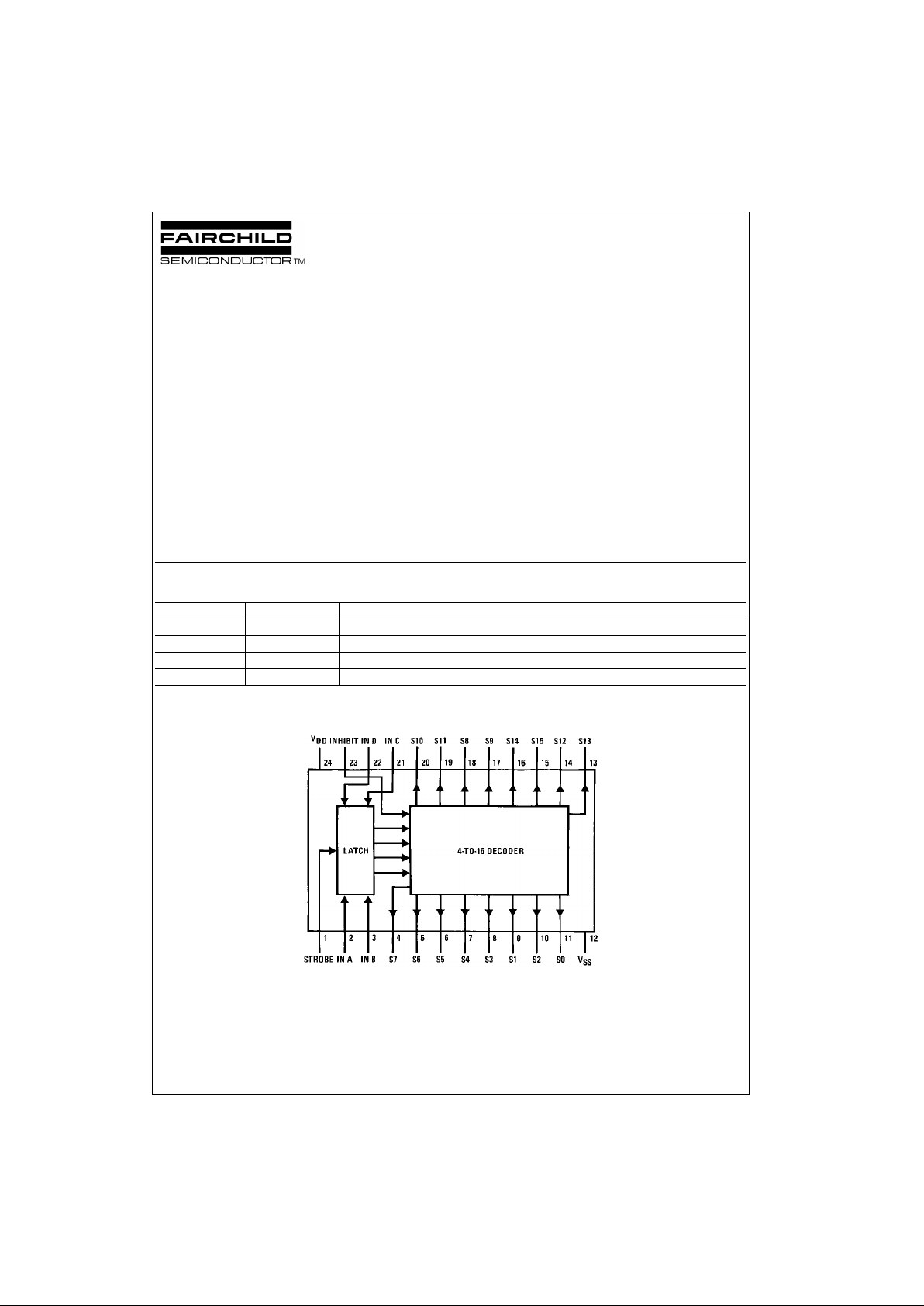
Connection Diagram
Top View
Order Number Package Number Package Diagram
CD4514BCWM M24B 24-Lead Small Outline Integrated Circuit (SOIC), JEDEC MS-013, 0.300 Wide
CD4514BCN N24A 24-Lead Pla sti c Dual-In-Line Package (PDIP), JEDEC MS-0 11, 0.600 Wide
CD4515BCWM M24B 24-Lead Small Outline Integrated Circuit (SOIC), JEDEC MS-013, 0.300 Wide
CD4515BCN N24A 24-Lead Pla sti c Dual-In-Line Package (PDIP), JEDEC MS-0 11, 0.600 Wide

www.fairchildsemi.com 2
CD4514BC• CD4515BC
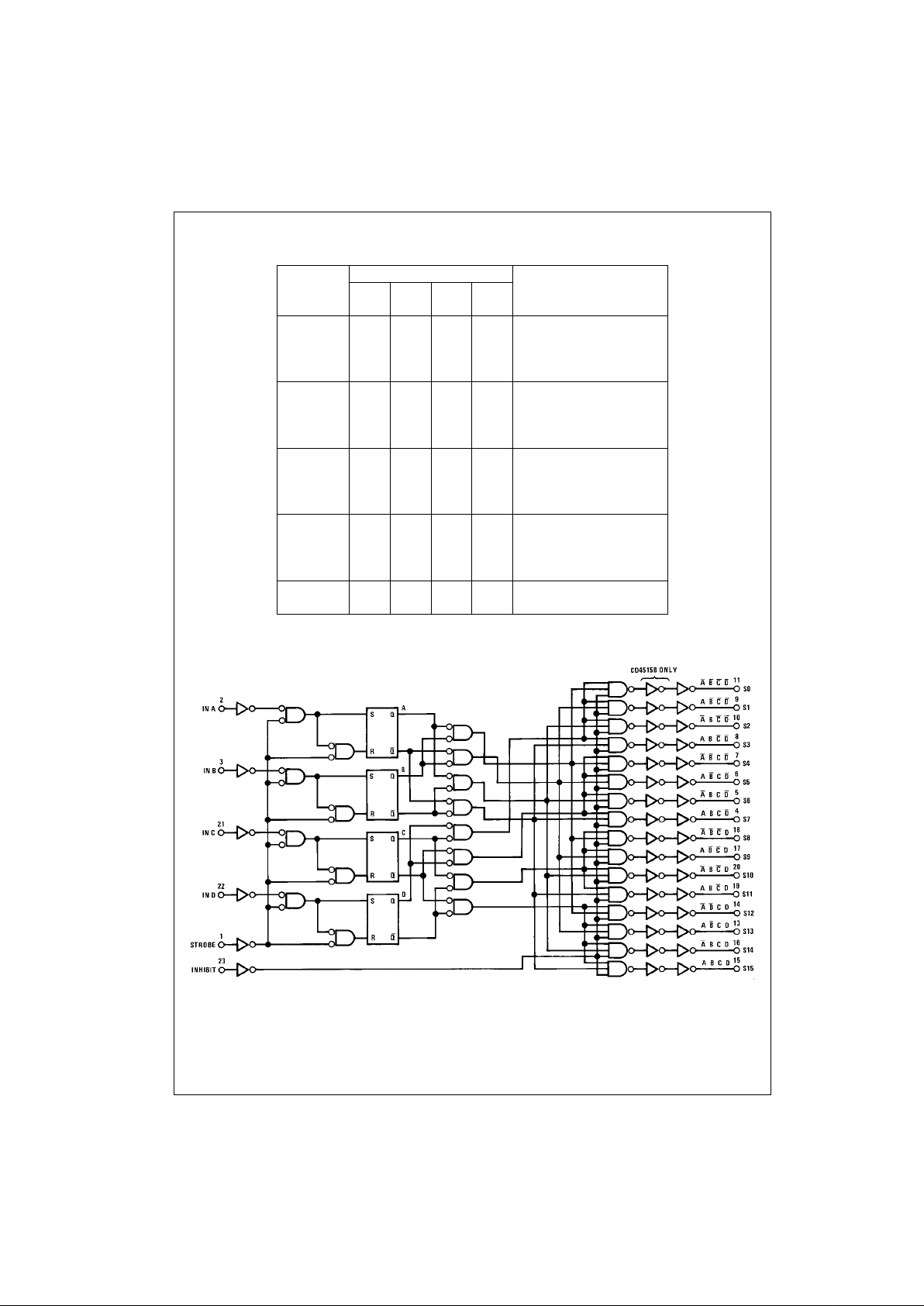
Truth Table
Decode Truth Table (Strobe = 1)
X = Don’t Care
Logic Diagram
Data Inputs Selected Output
Inhibit D C B A CD4514
= Logic “1”
CD4515
= Logic “0”
0 0 0 0 0 S0
0 0 0 0 1 S1
0 0 0 1 0 S2
0 0 0 1 1 S3
0 0 1 0 0 S4
0 0 1 0 1 S5
0 0 1 1 0 S6
0 0 1 1 1 S7
0 1 0 0 0 S8
0 1 0 0 1 S9
0 1 0 1 0 S10
0 1 0 1 1 S11
0 1 1 0 0 S12
0 1 1 0 1 S13
0 1 1 1 0 S14
0 1 1 1 1 S15
1 X X X X All Outputs
= 0, CD4514
All Outputs
= 1, CD4515

3 www.fairchildsemi.com
CD4514BC• CD4515BC
Absolute Maximum Ratings(Note 1)
(Note 2)
Recommended Operating
Conditions
(Note 2)
Note 1: “Absolute Maximum Ratings” are those values bey ond which the
safety of the device cannot be guaranteed. Except for “Operating Temperature Range” they are not meant to imply that the devic es should be operated at these limit s. The tables of “Recommended O perating Condit ions”
and “Electrical Characteristics” provide conditions for actual device opera-
tion.
Note 2: V
SS
= 0V unless otherw is e s pecified.
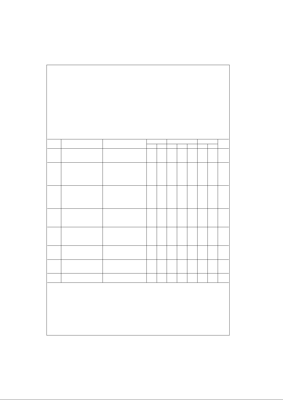
DC Electrical Characteristics (Note 2)
CD4514BC, CD4515BC
Note 3: IOH and IOL are tested one output at a ti m e.
DC Supply Voltage (VDD) −0.5V to +18V
Input Voltage (V
IN
) −0.5V to VDD + 0.5V
Storage Temperature Range (T
S
) −65°C to +150°C
Power Dissipation (P
D
)
Dual-In-Line 700 mW
Small Outline 500 mW
Lead Temperature (T
L
)
(Soldering, 10 seconds) 260
°C
DC Supply Voltage (V
DD
) 3V to 15V
Input Voltage (V
IN
) 0V to V
DD
Operating Temperature Range (TA)
CD4514BC, CD4515BC
−40°C to +85°C
Symbol Parameter Conditions
−40°C +25°C +85°C
Units
Min Max Min Typ Max Min Max
I
DD
Quiescent Device VDD = 5V, VIN = VDD or V
SS
20 0.005 20 150 µA
Current VDD = 10V, VIN = VDD or V
SS
40 0.010 40 300 µA
V
DD
= 15V, VIN = VDD or V
SS
80 0.015 80 600 µA
V
OL
LOW Level VIL = 0V, VIH = VDD,
Output Voltage |IO| < 1 µA
V
DD
= 5V 0.05 0 0.05 0.05 V
V
DD
= 10V 0.05 0 0.05 0.05 V
VDD = 15V 0.05 0 0.05 0.05 V
V
OH
HIGH Level VIL = 0V, VIH = VDD,
Output Voltage |I
O
| < 1 µA
VDD = 5V 4.95 4.95 5.0 4.95 V
V
DD
= 10V 9.95 9.95 10.0 9.95 V
V
DD
= 15V 14.95 14.95 15.0 14.95 V
V
IL
LOW Level |IO| < 1 µA
Input Voltage V
DD
= 5V, VO = 0.5V or 4.5V 1.5 2.25 1.5 1.5 V
V
DD
= 10V, VO = 1.0V or 9.0V 3.0 4.50 3.0 3.0 V
VDD = 15V, VO = 1.5V or 13.5V 4.0 6.75 4.0 4.0 V
V
IH
HIGH Level |IO| < 1 µA
Input Voltage V
DD
= 5V, VO = 0.5V or 4.5V 3.5 3.5 2.75 3.5 V
VDD = 10V, VO = 1.0V or 9.0V 7.0 7.0 5.50 7.0 V
V
DD
= 15V, VO = 1.5V or 13.5V 11.0 11.0 8.25 11.0 V
I
OL
LOW Level Output VDD = 5V, VO = 0.4V 0.52 0.44 0.88 0.36 mA
Current (Note 3) VDD = 10V, VO = 0.5V 1.3 1.1 2.25 0.90 mA
VDD = 15V, VO = 1.5V 3.6 3.0 8.8 2.4 mA
I
OH
HIGH Level Output VDD = 5V, VO = 4.6V −0.52 −0.44 −0.88 −0.36 mA
Current (Note 3) VDD = 10V, VO = 9.5V −1.3 −1.1 −2.25 −0.90 mA
VDD = 15V, VO = 13.5V −3.6 −3.0 −8.8 −2.4 mA
I
IN
Input Current VDD = 15V, VIN = 0V −0.3 −10−5 −0.3 −1.0 µA
VDD = 15V, VIN = 15V 0.3 10−5 0.3 1.0 µA
 Loading...