Fairchild Semiconductor CD4512BCN, CD4512BCMX, CD4512BCM, CD4512BCCW Datasheet

October 1987
Revised January 1999
CD4512BC 8-Channel Buffered Data Selector
© 1999 Fairchild Semiconductor Corporation DS005993.prf www.fairchildsemi.com
CD4512BC
8-Channel Buffered Data Selector
General Description
The CD4512BC buffered 8-channel da ta se lecto r is a com plementary MOS (CMOS) circuit constructed with N- and
P-channel enhancement mode transistors. This data selec tor is primarily used as a digital signal multiplexer selecting
1 of 8 inputs and routing the signal to a 3-STATE output. A
high level at the Inhibit input forces a low level at the output. A high level at the Output Enable
(OE) input forces the
output into the 3-STATE condition. Low levels at both the
Inhibit and (OE
) inputs allow normal operation.
Features
■ Wide supply voltage range: 3.0V to 15V
■ High noise immunity: 0.45 V
DD
(typ.)
■ 3-STATE output
■ Low quiescent power dissipation:
0.25 µW/package (typ.) @ V
CC
= 5.0V
■ Plug-in replacement for Motorola MC14512
Ordering Code:
Devices also available in Tape and Reel. Specify by appending suffix “X” to the order ing code.
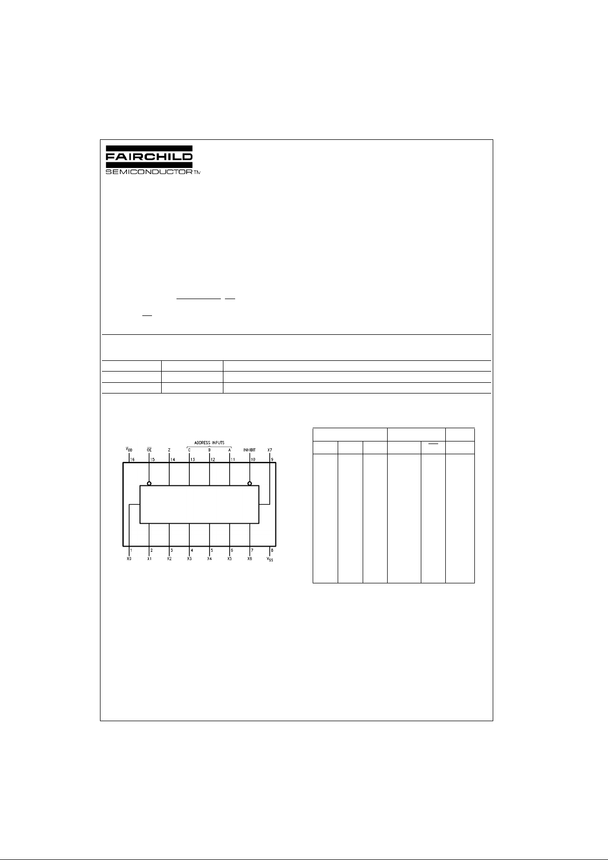
Connection Diagram
Pin Assignments for SOIC an d DIP
Top View
Truth Table
2 = Don't care
Hi-Z = 3-STATE condition
Xn = Data at input n
Order Number Package Number Package Description
CD4512BCM M16A 16-Lead Small Outline Integrated Circuit (SOIC), JEDEC MS-012, 0.150” Narrow Body
CD4512BCN N16E 16-Lead Plastic Dual-In-Line Package (PDIP), JEDEC MS-001, 0.300” Wide
Address Inputs Control Inputs Output
C B A Inhibit OE
Z
000 0 0 X0
001 0 0X1
0 10 0 0X2
011 0 0X3
100 0 0 X4
101 0 0X5
1 10 0 0X6
111 0 0X7
211 1 0 0
2 2 2 2 1 Hi-Z

www.fairchildsemi.com 2
CD4512BC
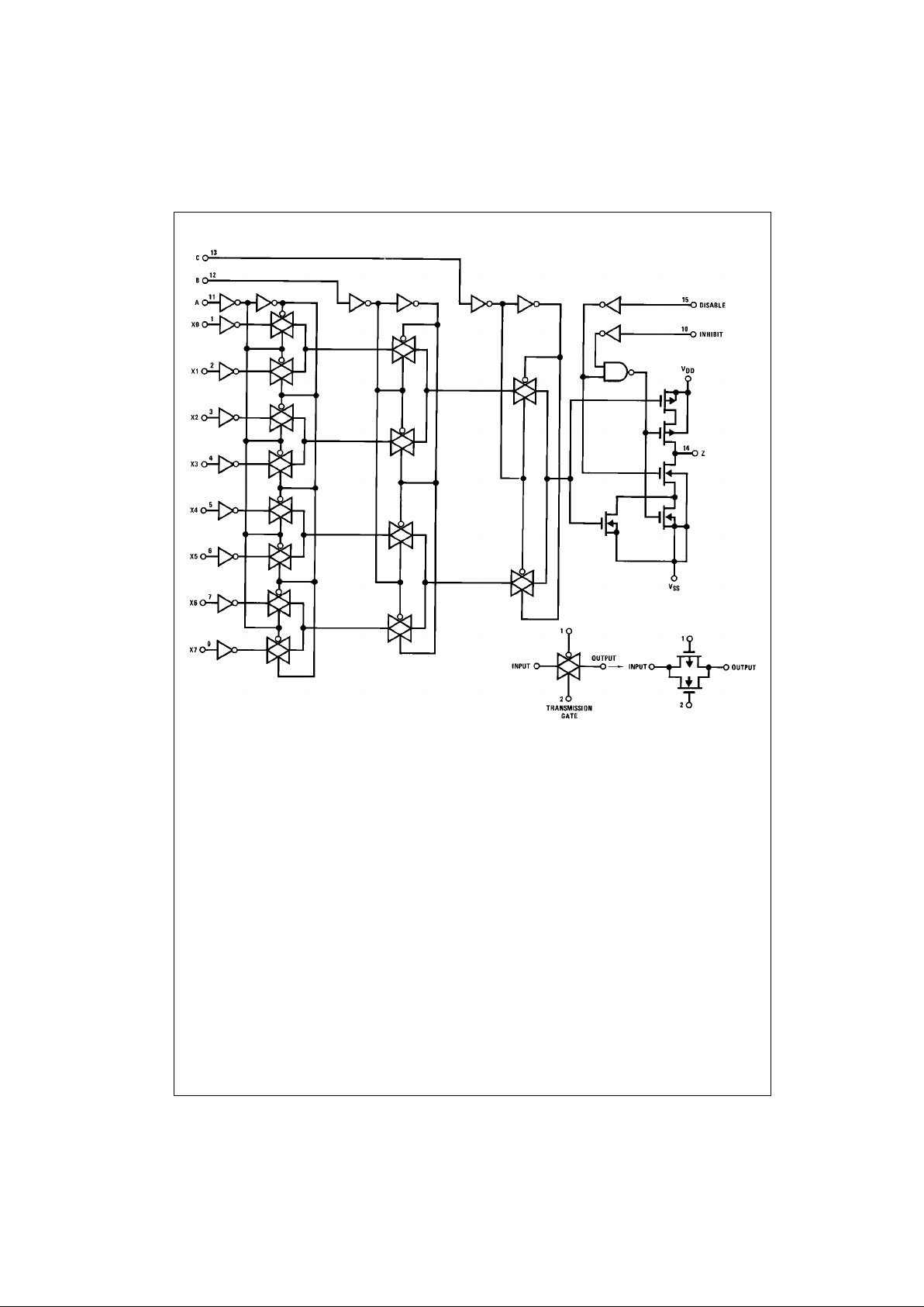
Logic Diagram

3 www.fairchildsemi.com
CD4512BC
Absolute Maximum Ratings(Note 1)
(Note 2)
Recommended Operating
Conditions
(Note 2)
Note 1: “Absolute Maximum Rat ings” are tho se values beyond which the
safety of the device cannot be guaranteed. They are not meant to imply
that the devices shoul d be operated at these limits. The Recommend ed
Operating Conditio ns and Electrical Characteris tics table provide conditions for actual device operatio n.
Note 2: V
SS
= 0V unless otherw is e s pecified.
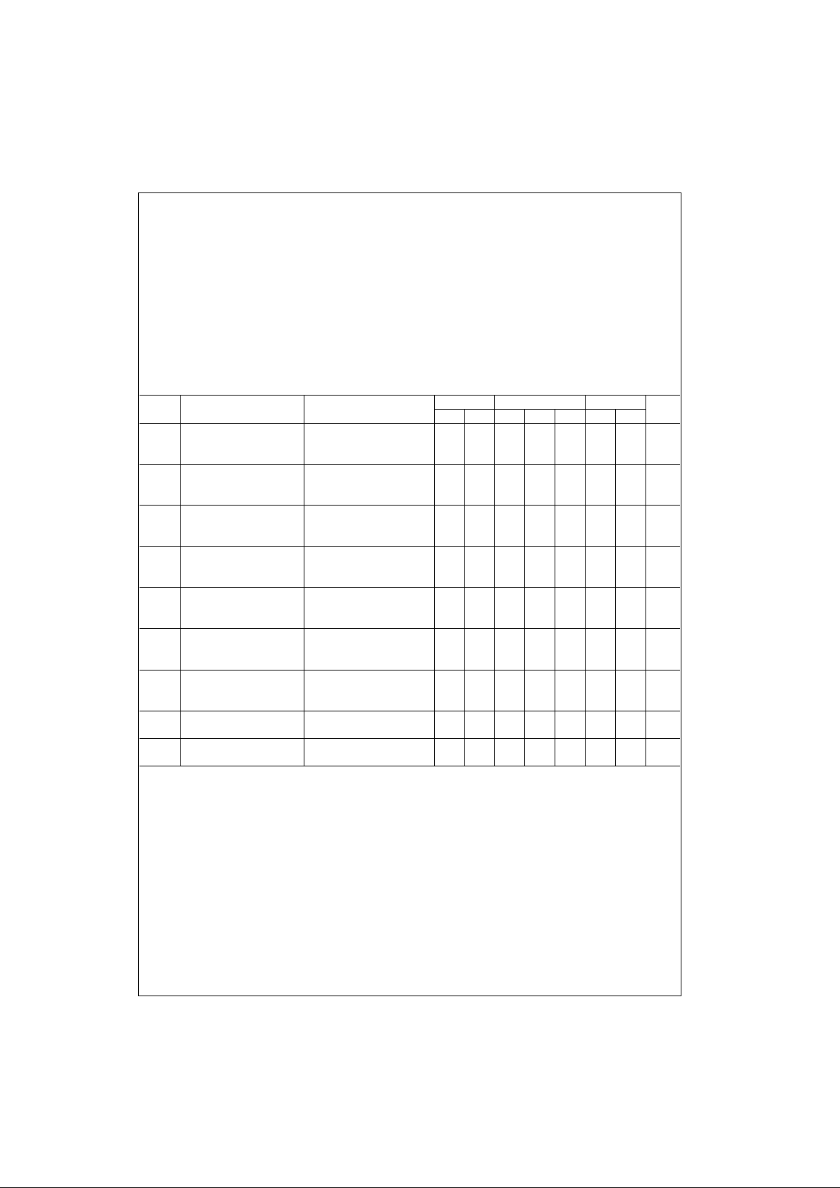
DC Electrical Characteristics (Note 2)
Note 3: IOH and IOL are tested one output at a ti m e.
Supply Voltage (VDD) −0.5 to +18 V
DC
Input Voltage (VIN) −0.5 to VDD + 0.5 V
DC
Storage Temperatur e Range (TS) −65°C to +150°C
Power Dissipa tion (P
D
)
Dual-In-Line 700 mW
Small Outline 500 mW
Lead Temperature, (T
L
)
(Soldering, 10 seconds) 260°C
DC Supply Voltage (V
DD
) 3.0 to 15 V
DC
Input Voltage (VIN) 0 to VDD V
DC
Operating Temperature Range (TA) −40°C to +85°C
Symbol Parameter Conditions
−40°C +25°C +85°C
Units
Min Max Min Typ Max Min Max
I
DD
Quiescent Device VDD = 5V, VIN = VDD or V
SS
20 0.005 20 150 µA
Current VDD = 10V, VIN = VDD or V
SS
40 0.010 40 300 µA
VDD = 15V, VIN = VDD or V
SS
80 0.015 80 600 µA
V
OL
LOW Level VDD = 5V 0.05 0 0.05 0.05 V
Output Voltage VDD = 10V |IOL| < 1 µA 0.05 0 0.05 0.05 V
VDD = 15V 0.05 0 0.05 0.05 V
V
OH
HIGH Level VDD = 5V 4.95 4.95 5.0 4.95 V
Output Voltage VDD = 10V |I
OH
| < 1 µA 9.95 9.95 10.0 9.95 V
VDD = 15V 14.95 14.95 15.0 14.95 V
V
IL
LOW Level VDD = 5V, VO = 0.5V 1.5 2.25 1.5 1.5 V
Input Voltage VDD = 10V, VO = 1.0V 3.0 4.50 3.0 3.0 V
VDD = 15V, VO = 1.5V 4.0 6.75 4.0 4.0 V
V
IH
HIGH Level VDD = 5V, VO = 4.5V 3.5 3.5 2.75 3.5 V
Input Voltage VDD = 10V, VO = 9.0V 7.0 7.0 5.50 7.0 V
VDD = 15V, VO = 13.5V 11.0 11.0 8.25 11.0 V
I
OL
LOW Level Output VDD = 5V, VO = 0.4V 0.52 0.44 0.78 0.36 mA
Current VDD = 10V, VO = 0.5V 1.3 1.1 2.0 0.9 mA
(Note 3) VDD = 15V, VO = 1.5V 3.6 3.4 7.8 2.4 mA
I
OH
HIGH Level Output VDD = 5V, VO = 4.6V −0.2 −0.16 −0.12 mA
Current VDD = 10V, VO = 9.5 −0.5 −0.4 −0.3 mA
(Note 3) VDD = 15V, V O = 13.5V −1.4 −1.2 −1.0 mA
I
IN
Input Current VDD = 15V, VIN = 0V −0.3 −10−5−0.3 −1.0 µA
VDD = 15V, VIN = 15V 0.3 10−50.3 1.0 µA
I
OZ
3-STATE VDD = 15V, VO = 0V ±1.0 ±10
−5
±1.0 ±7.5 µA
Output Current VDD = 15V, VO = 15V
 Loading...