Fairchild Semiconductor CD4511BCWMX, CD4511BCWM, CD4511BCN Datasheet

October 1987
Revised January 1999
CD4511BC BCD-to-7 Segment Latch/Decoder/Driver
© 1999 Fairchild Semiconductor Corporation DS005991.prf www.fairchildsemi.com
CD4511BC
BCD-to-7 Segment Latch/Decoder/Driver
General Description
The CD4511BC BCD-to-seven segment latch/decoder/
driver is constructed with complementary MOS (CMOS)
enhancement mode devices and NPN bipolar output drivers in a single monolithic structure. The circuit provides the
functions of a 4-bit storage la tch, an 8421 BCD-to-seven
segment decoder, and an output drive capability. Lamp test
(LT), blanking (BI), and latch enable (LE) inputs are used to
test the display, to turn-off or pulse modulate the brightness
of the display, and to store a BCD code, respectively. It can
be used with seven-segment ligh t emitting diodes (LED),
incandescent, fluorescent , gas discharge, or liquid cr ystal
readouts either dire ctly or indirectly.
Applications include instr ument (e.g., counter, DVM, etc.)
display driver, computer/calculator display driver, cockpit
display driver, and various clock, watch, and timer uses.
Features
■ Low logic circuit power dissipation
■ High current sourcing outputs (up to 25 mA)
■ Latch storage of code
■ Blanking input
■ Lamp test provision
■ Readout blanking on all illegal input combinations
■ Lamp intensity modulation capability
■ Time share (multiplexing) facility
■ Equivalent to Motorola MC14511
Ordering Code:
Devices also available in Tape and Reel. Specify by appending suffix letter “X” to the ordering code.
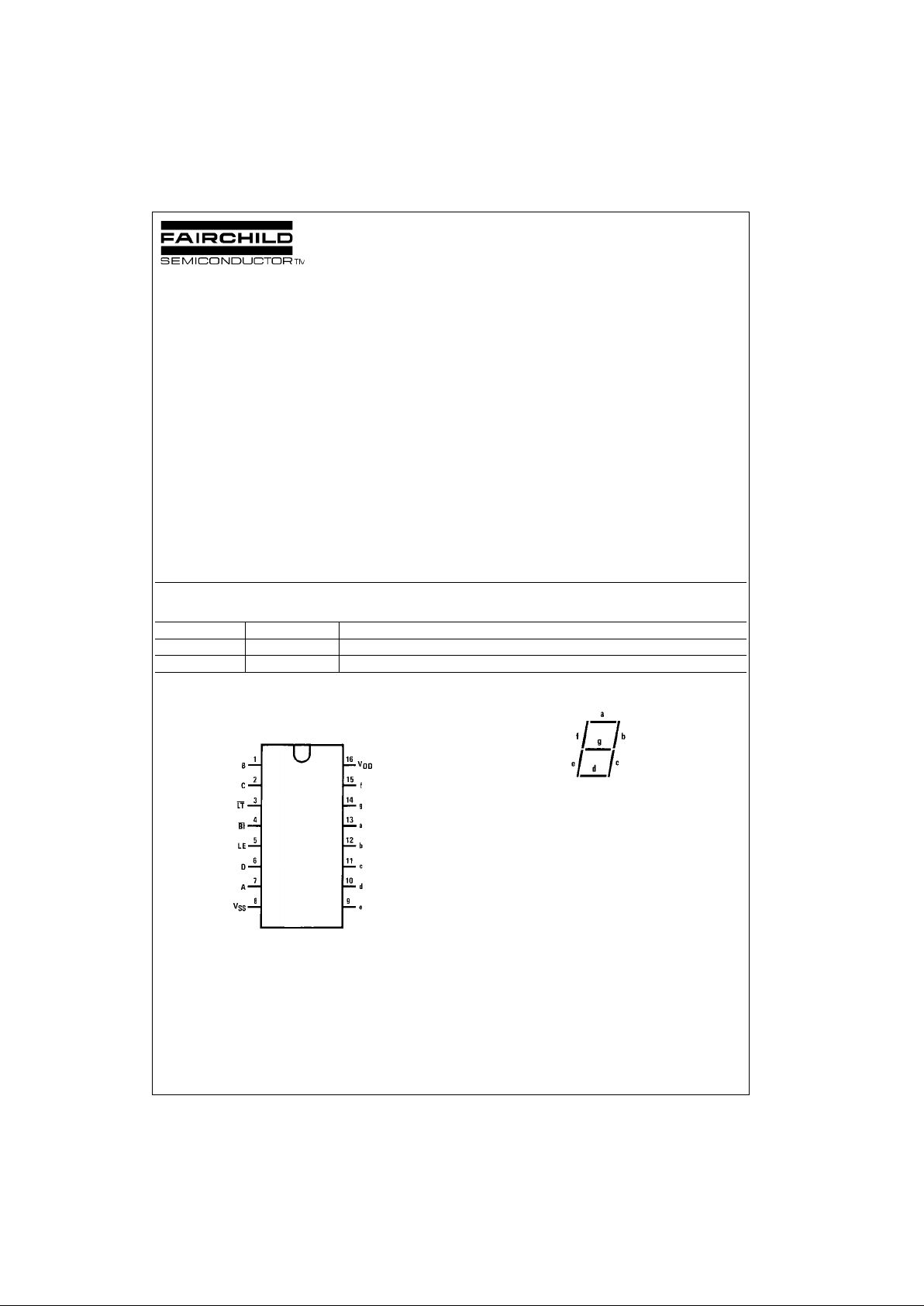
Connection Diagrams
Pin Assignments for SOIC and DIP
Top View
Segment Identification
Order Number Package Number Package Description
CD4511BCWM M16B 16-Lead Small Outline Integrated Circuit (SOIC), JEDEC MS-013, 0.300” Wide
CD4511BCN N16E 16-Lead Plastic Dual-In-Line Package (PDIP), JEDEC MS-001, 0.300” Wide

www.fairchildsemi.com 2
CD4511BC
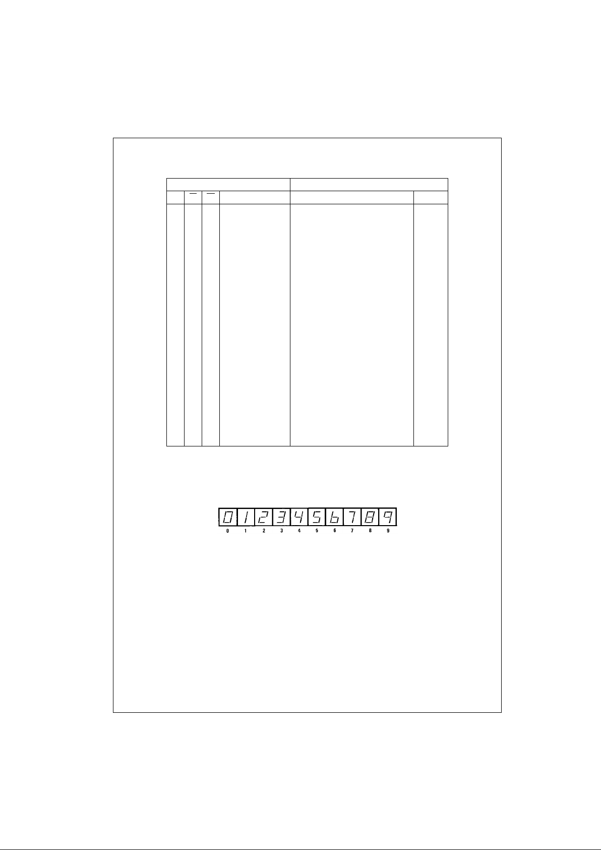
Truth Table
X = Don’t Care
*Depends upon th e BCD code applied du ring the 0 to 1 transition of LE.
Display
Inputs Outputs
LE BI
LT DCBAa bcd e f gDisplay
XX0 XXXX11 11111 B
X01XX XX0000 000
011000 011111 10 0
0 110001 011000 0 1
01 100101 101101 2
011 001111 11001 3
01101 000110 011 4
011010 110110 11 5
0 110110 001111 1 6
01 101111 110000 7
011 100011 11111 8
01110 011110 011 9
011101 000000 00
0 111011 000000 0
01 111000 000000
0111 101000 0000
011111 000000 00
0 111111 000000 0
1 1 1XXXX * *

3 www.fairchildsemi.com
CD4511BC
Absolute Maximum Ratings(Note 1) Recommended Operating
Conditions
Note 1: Devices should not be connected with power on.
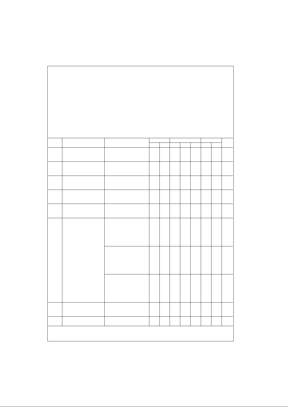
DC Electrical Characteristics
DC Supply Voltage (VDD) −0.5V to +18V
Input Voltage (V
IN
) −0.5V to VDD +0.5V
Storage Temperature Range (T
S
) −65°C to +150°C
Power Dissipation (P
D
)
Dual-In-Line 700 mW
Small Outline 500 mW
Lead Temperature (T
L
)
(Soldering, 10 seconds ) 260°C
DC Supply Voltage (V
DD
) 3V to 15V
Input Voltage (V
IN
)0V to V
DD
Operating Temperature Range (TA) −40°C t o +85°C
Symbol Parameter Conditions
−40°C +25°C +85°C
Units
Min Max Min Typ Max Min Max
I
DD
Quiescent VDD = 5V 20 20 150 µA
Supply Current VDD = 10V 40 40 300 µA
VDD = 15V 80 80 600 µA
V
OL
Output Voltage VDD = 5V 0.01 0 0.01 0.05 V
Logical “0” VDD = 10V 0.01 0 0.01 0.05 V
Level VDD = 15V 0.01 0 0.01 0.05 V
V
OH
Output Voltage VDD = 5V 4.1 4.1 4.57 4.1 V
Logical “1” VDD = 10V 9.1 9.1 9.58 9.1 V
Level VDD = 15V 14.1 14.1 14.59 14.1 V
V
IL
LOW Level VDD = 5V, V
OUT
= 3.8V or 0.5V 1.5 2 1.5 1.5 V
Input Voltage VDD = 10V, V
OUT
= 8.8V or 1.0V 3.0 4 3.0 3.0 V
VDD = 15V, V
OUT
= 13.8V or 1.5V 4.0 6 4.0 4.0 V
V
IH
HIGH Level VDD = 5V, V
OUT
= 0.5V or 3.8V 3.5 3.5 3 3.5 V
Input Voltage VDD = 10V, V
OUT
= 1.0V or 8.8V 7.0 7.0 6 7.0 V
VDD = 15V, V
OUT
= 1.5V or 13.8V 11.0 11.0 9 11.0 V
V
OH
Output VDD = 5V, IOH = 0 mA 4.1 4.1 4.57 4.1 V
(Source) Drive VDD = 5V, IOH = 5 mA 4.24 V
Voltage VDD = 5V, IOH = 10 mA 3.6 3.6 4.12 3.3 V
VDD = 5V, IOH = 15 mA 3.94 V
VDD = 5V, IOH = 20 mA 2.8 2.8 3.75 2.5 V
VDD = 5V, I
OH
= 25 mA 3.54 V
VDD = 10V, IOH = 0 mA 9.1 9.1 9.58 9.1 V
VDD = 10V, IOH = 5 mA 9.26 V
VDD = 10V, IOH = 10 mA 8.75 8.75 9.17 8.45 V
VDD = 10V, I
OH
= 15 mA 9.04 V
VDD = 10V, IOH = 20 mA 8.1 8.1 8.9 7.8 V
VDD = 10V, IOH = 25 mA 8.75 V
VDD = 15V, IOH = 0 mA 14.1 14.1 14.59 14.1 V
VDD = 15V, I
OH
= 5 mA 14.27 V
VDD = 15V, IOH = 10 mA 13.75 13.75 14.18 13.45 V
VDD = 15V, IOH = 15 mA 14.07 V
VDD = 15V, IOH = 20 mA 13.1 13.1 13.95 12.8 V
VDD = 15V, I
OH
= 25 mA 13.8 V
I
OL
LOW Level VDD = 5V, VOL = 0.4V 0.52 0.44 0.88 0.36 mA
Output Current VDD = 10V, VOL = 0.5V 1.3 1.1 2.25 0.9 mA
VDD = 15V, VOL = 1.5V 3.6 3.0 8.8 2.4 mA
I
IN
Input Current VDD = 15V, VIN = 0V −0.30 −10−5−0.30 −1.0 µA
VDD = 15V, VIN = 15V 0.30 10−50.30 1.0 µA
 Loading...