Fairchild Semiconductor CD4030CSJX, CD4030CSJ, CD4030CN Datasheet

October 1987
Revised January 1999
CD4030C Quad EXCLUSIVE-OR Gate
© 1999 Fairchild Semiconductor Corporation DS005961.prf www.fairchildsemi.com
CD4030C
Quad EXCLUSIVE-OR Gate
General Description
The CD4030C EXCLU SIVE-O R gat es are monol ithi c complementary MOS (CMOS) integrated circuits c onstructed
with N- and P-channel enha ncement mode transist ors. All
inputs are protected against static discharge with diodes to
V
DD
and VSS.
Features
■ Wide supply voltage range: 3.0V to 15V
■ Low power: 100 nW (typ.)
■ Medium speed operation:
t
PHL
= t
PLH
= 40 ns (typ.) at CL = 15 pF, 10V supply
■ High noise immunity 0.45 V
CC
(typ.)
Applications
• Automotive
• Data terminals
• Instrumentation
• Medical electronics
• Industrial controls
• Remote metering
• Computers
Ordering Code:
Device also available in Tape and Reel. Specify by appendin g s uf f ix let t er “X” to the ordering co de.
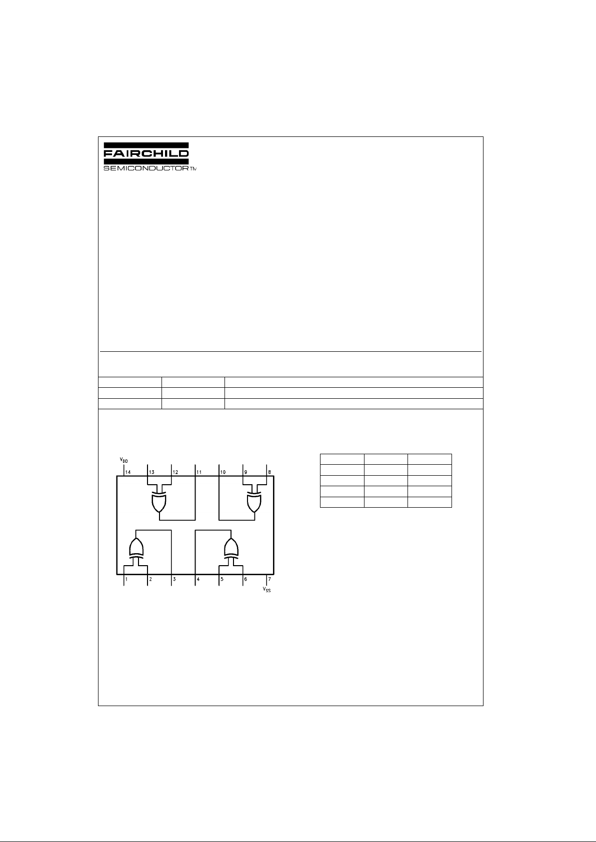
Connection Diagram
Pin Assignments for DIP and SOP
Truth Table
1 = HIGH Level
0 = LOW Level
Order Number Package Number Package Description
CD4030CSJ M14D 14-Lead Small Outline Package (SOP), EIAJ TYPE II, 5.3mm Wide
CD4030CN N14A 14-Lead Plastic Dual-In-Line Package (PDIP), JEDEC MS-001, 0.300” Wide
A B J
0 0 0
1 0 1
0 1 1
1 1 0

www.fairchildsemi.com 2
CD4030C
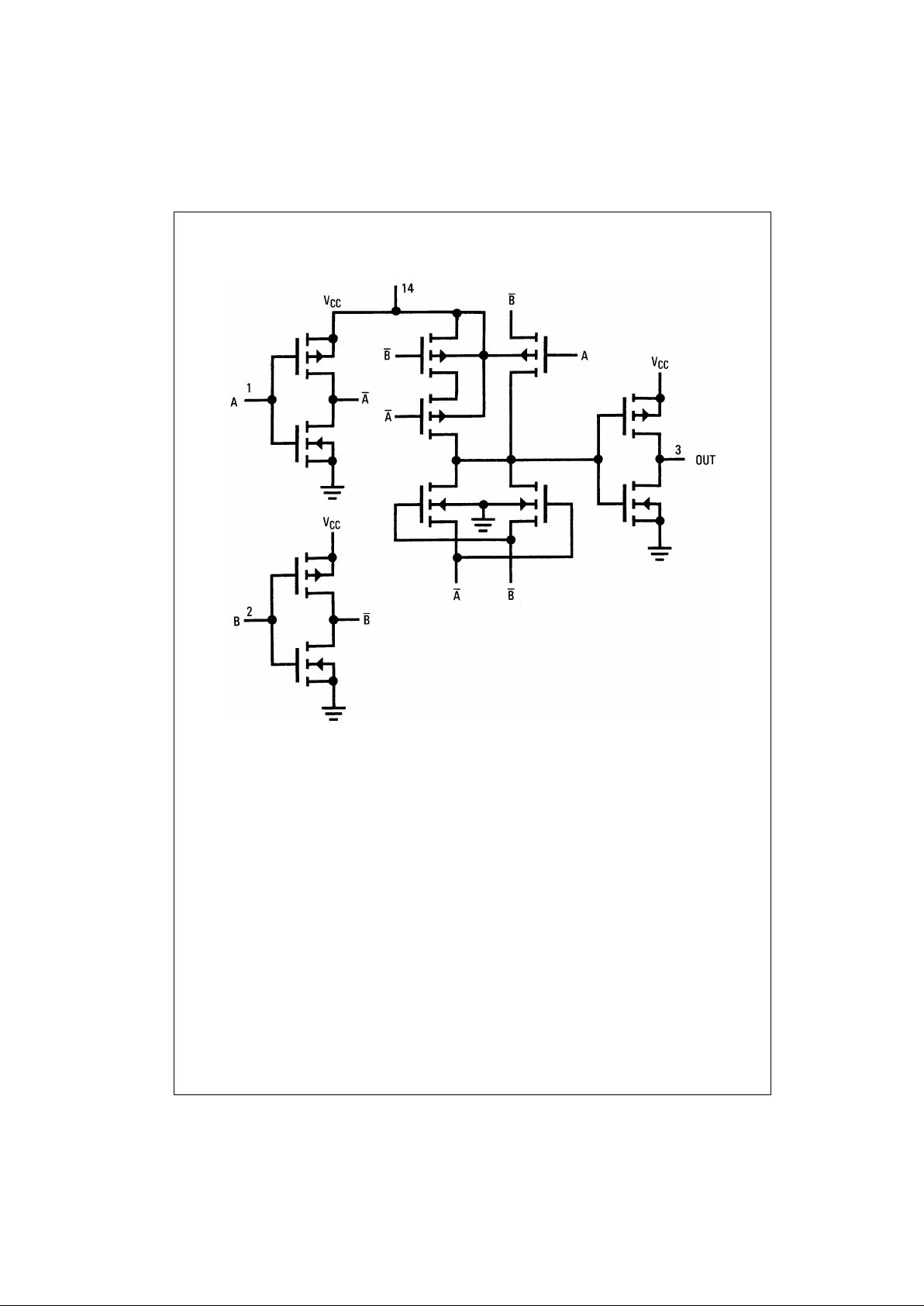
Logic Diagram
 Loading...