

Fairchild Semiconductor BSR56 Datasheet
BSR56
N-Channel Low-Frequency Low-Noise
Amplifier
• This device is designed for low-power chopper or switching application
sourced from process 51
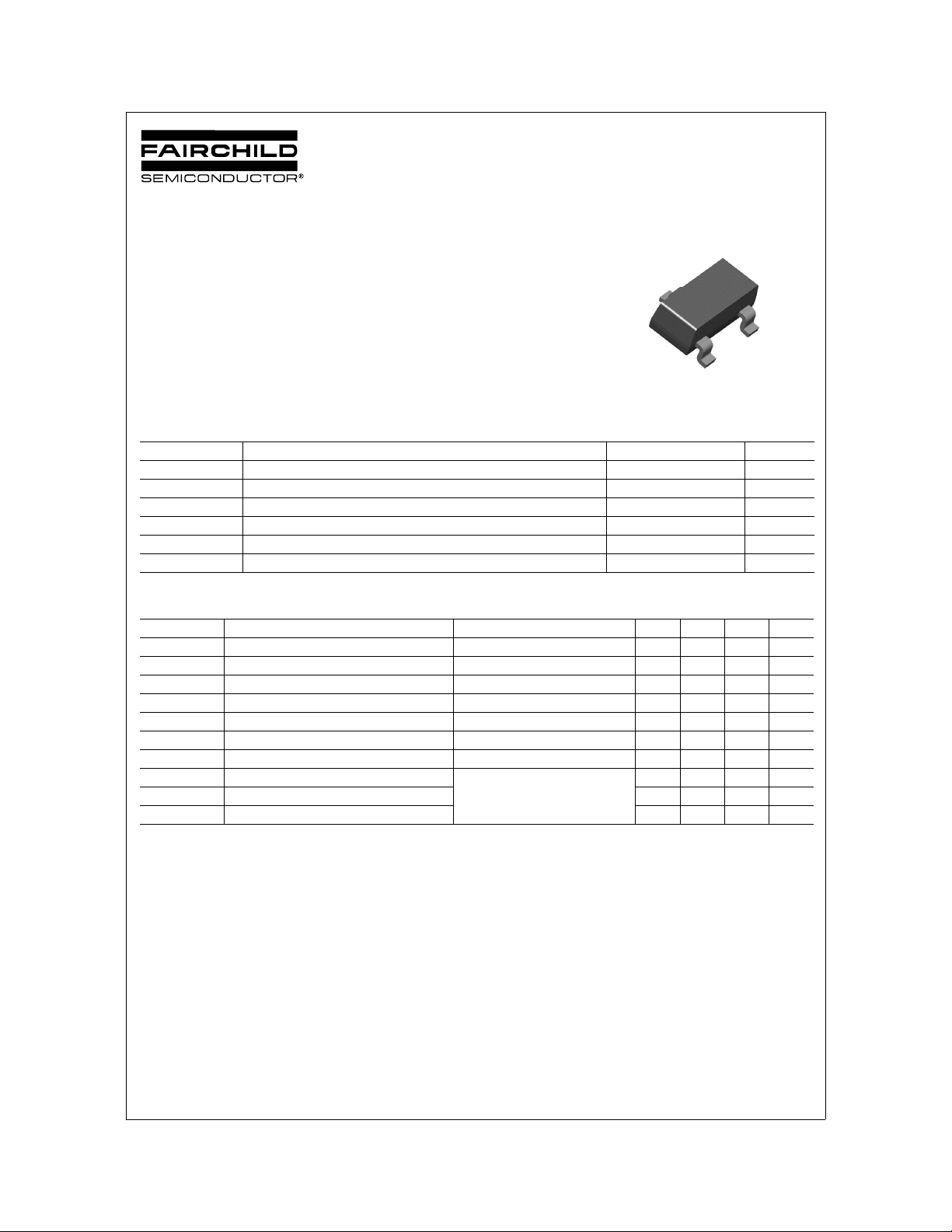
3
2
SOT-23
1
Mark: M4
1. Drain 2. Source 3. Gate
BSR56
Absolute Maximum Ratings T
=25°C unless otherwise noted
C
Symbol Parameter Value Units
V
DGO
V
GSO
I
GF
P
tot
T
STG
T
J
Electrical Characteristics
Drain-Gate Voltage 40 V
Gate-Source Voltage - 40 V
Forward Gate Current 50 mA
Total Power Dissipation up to T
=40°C 250 mW
amb
Storage Temperature Range - 55 ~ 150 °C
Junction Temperature 150 °C
TC=25°C unless otherwise noted
Symbol Parameter Test Condition Min. Typ. Max. Units
BV
GSS
I
GSS
I
DSS
(off) Gate-Sou r c e Cut-off Voltage VDS = 15V, ID = 0.5nA 4 10 V
V
GS
(on) Drain-Source On Voltage VGS = 0V, ID = 20mA 750 mV
V
DS
(on) Drain-Source On Reverse VGS = 0V, ID = 0 25 Ω
r
ds
C
rss
t
d
t
r
t
off
Gate-Source Voltage VDS = 0V, IC = 1µA40 V
Gate Reverse Current VGS = 20V 1 nA
Zero-Gate Voltage Drain Current VDS = 15V, VGS = 0V 50 mA
Reverse Transfer Capacitance VDS = 10V, VGS = 0V 5 pF
Delay Time VDD = 10V, VGS(on) = 0V
= 20mA, VGS(off) = 10V
I
Rise Time 3nS
D
6nS
Turn-off Time 25 nS
©2002 Fairchild Semiconductor Corporation Rev. A1, November 2002
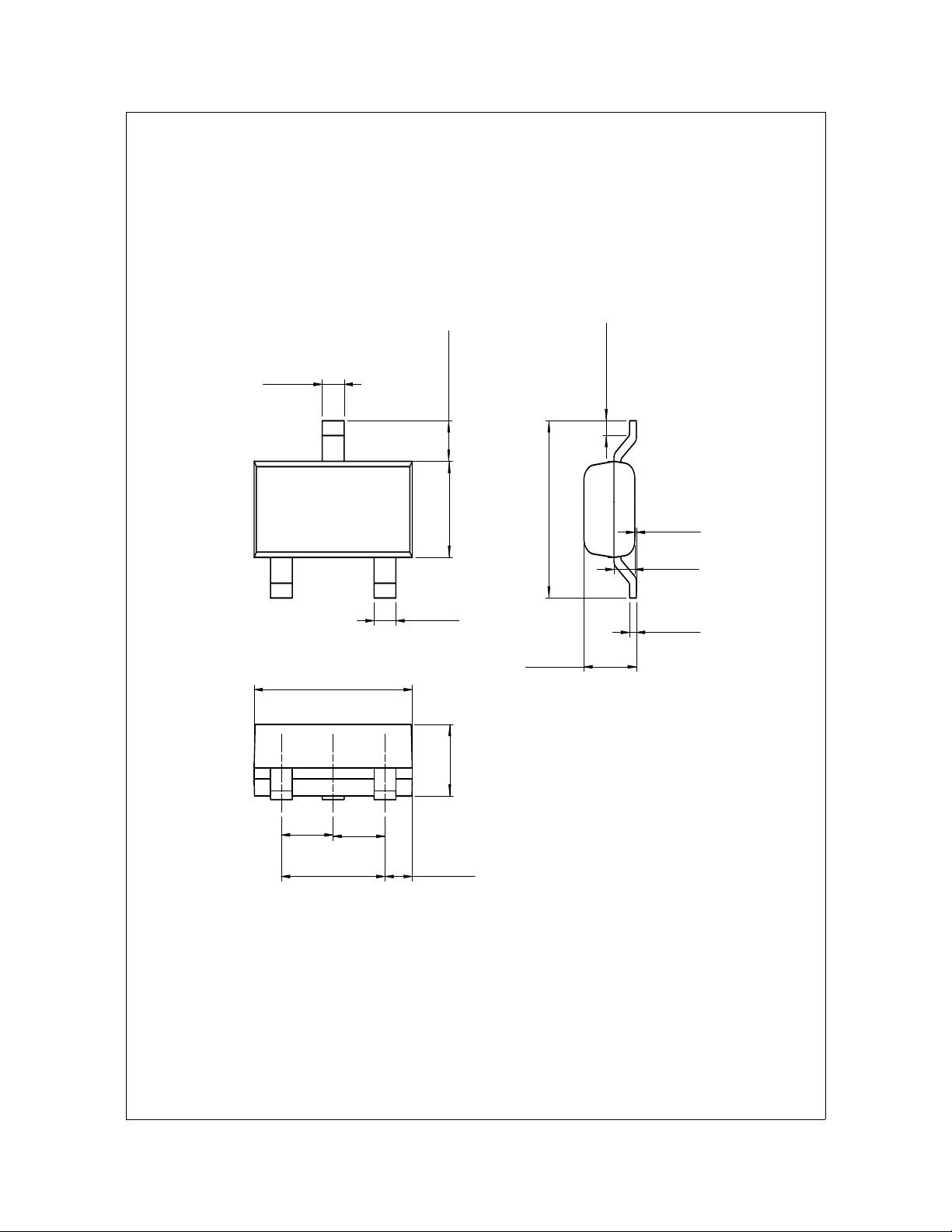
Package Dimensions
0.40
±0.03
BSR56
SOT-23
0.20 MIN
0.45~0.60
0.95
2.90
±0.03
1.90
±0.10
0.95
±0.03
±0.03
±0.10
0.40
±0.03
0.97REF 1.30
0.508REF
±0.10
2.40
0.96~1.14
0.03~0.10
0.38 REF
+0.05
0.12
–0.023
Dimensions in Millimeters
©2002 Fairchild Semiconductor Corporation Rev. A1, November 2002
 Loading...