

Fairchild Semiconductor 100352QIX, 100352QI, 100352QCX, 100352QC, 100352PC Datasheet
© 2000 Fairchild Semiconductor Corporation DS010248 www.fairchildsemi.com
October 1989
Revised August 2000
100352 Low Power 8-Bit Buffer with Cut-Off Drivers
100352
Low Power 8-Bit Buffer with Cut-Off Drivers
General Description
The 100352 contains an 8-b it bu ffer, individual inputs ( Dn),
outputs (Q
n
), and a data output enable pin (OEN). A Q out-
put follows its D input when the OEN
pin is LOW. A HIGH
on OEN
holds the outputs in a cut-off state. The cut-off
state is designed to be m ore negative than a n ormal ECL
LOW level. This allows the output emitter-followers to turn
off when the termin atio n s upp l y is
−2.0V, presenting a high
impedance to the data bus . This high impedan ce reduces
termination power and prevents loss of low state noise
margin when several loads share the bus.
The 100352 outpu ts are designe d to drive a doubly term inated 50
Ω transmission line (25Ω load impedance). All
inputs have 50 k
Ω pull-down resistors.
Features
■ Cut-off drivers
■ Drives 25
Ω load
■ Low power operation
■ 2000V ESD protection
■ Voltage compensated operating range
= −4.2V to −5.7V
■ Available to industrial grade temperature range
Ordering Code:
Devices also availab le in Tape and Reel. Specify by appending th e s uffix let t er “X” to the ordering code.
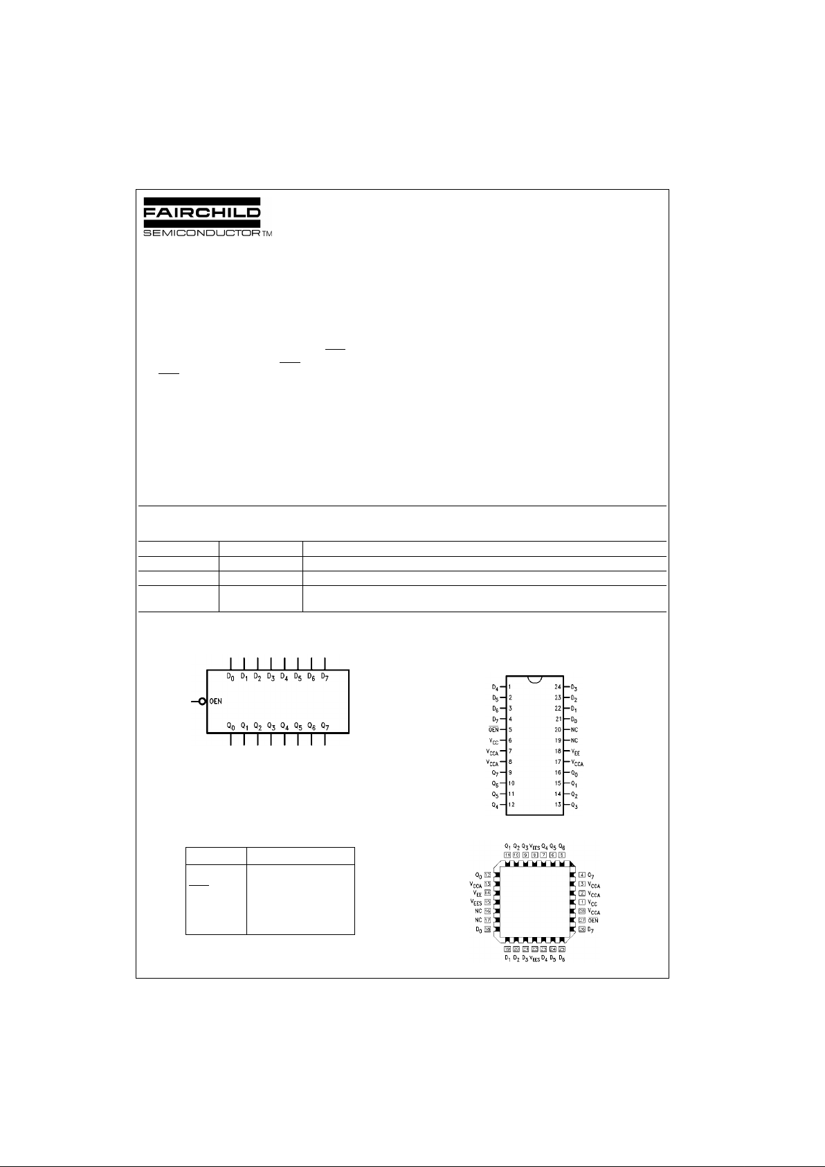
Logic Symbol
Pin Descriptions
Connection Diagrams
24-Pin DIP
28-Pin PLCC
Order Number Package Number Package Description
100352PC N24E 24-Lead Plastic Dual-In-Line Package (PDIP), JEDEC MS-010, 0.400 Wide
100352QC V28A 28-Lead Plastic Lead Chip Carrier (PLCC), JEDEC MO-047, 0.450 Square
100352QI V28A 28-Lead Plastic Lead Chip Carrier (PLCC), JEDEC MO-047, 0.450 Square
Industrial Temperature Range (
−40°C to +85°C)
Pin Names Description
D
0–D7
Data Inputs
OEN
Output Enable Input
Q
0–Q7
Data Outputs
NC No Connect
www.fairchildsemi.com 2
100352
Truth Table
H = HIGH Voltage Level
L = LOW Voltage Level
Cutoff = Lower-than-LOW State
X = Don’t Care
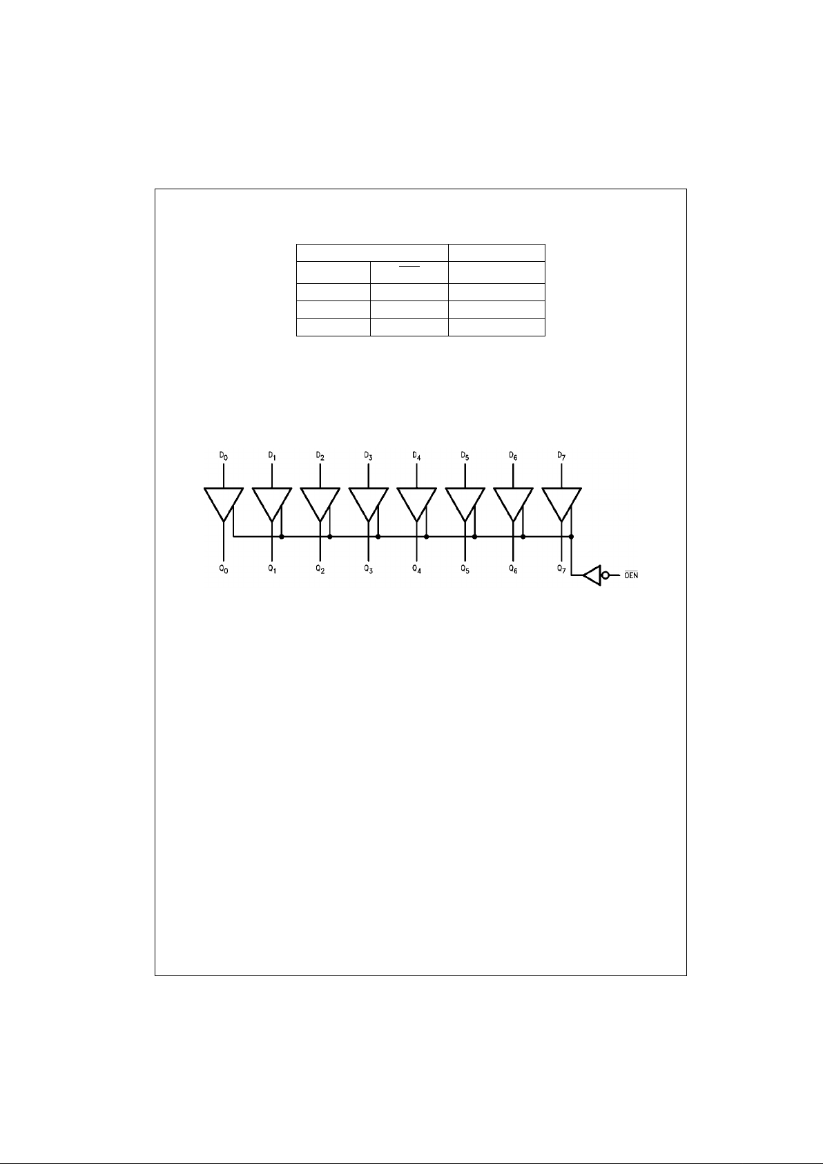
Logic Diagram
Inputs Outputs
D
n
OEN Q
n
LL L
HL H
XHCutoff
3 www.fairchildsemi.com
100352
Absolute Maximum Ratings(Note 1) Recommended Operating
Conditions
Note 1: The “Absolute Maximum Ratings” are those value s beyond which
the safety of the dev ice cannot b e guaranteed . The device sh ould not be
operated at these limit s. The parametric values defi ned in the Electrical
Characteristics tables are not guaranteed at the absolute maximum rating.
The “Recomm ended O peratin g Cond itions ” table will defin e the condition s
for actual device operation.
Note 2: ESD testing conforms to MIL-STD-883, Method 3015.
Commercial Version
DC Electrical Characteristics
(Note 3)
V
EE
= −4.2V to −5.7V, VCC = V
CCA
= GND, T
C
= 0°C to +85°C
Note 3: The specified limits represent the “worst case” value for the parameter. Since these values normally occur at the temperature extremes, additional
noise immunity and guardbanding can be achieved by decreasin g the al l owable syste m opera ti ng ran ge s. Cond it i ons fo r t estin g sho w n in the tabl es are chosen to guarantee operation under “worst case” conditions.
DIP AC Electrical Characteristics
V
EE
= −4.2V to −5.7V, VCC = V
CCA
= GND
Note 4: The propagation delay s pec ified is for single output swit c hing. Delays may vary up to 300 ps with multiple outpu ts s witching.
Storage Temperature (T
STG
) −65°C to +150°C
Maximum Junction Temperature (T
J
) +150°C
V
EE
Pin Potential to Ground Pin −7.0V to +0.5V
Input Voltage (DC) V
EE
to +0.5V
Output Current (DC Output HIGH)
−100 mA
ESD (Note 2)
≥2000V
Case Temperature (T
C
)
Commercial 0
°C to +85°C
Industrial
−40°C to +85°C
Supply Voltage (V
EE
) −5.7V to −4.2V
Symbol Parameter Min Typ Max Units Conditions
V
OH
Output HIGH Voltage −1025 −955 −870
mV
VIN =V
IH (Max)
Loading with
V
OL
Output LOW Voltage −1830 −1705 −1620 or V
IL (Min)
25Ω to −2.0V
V
OHC
Output HIGH Voltage −1035
mV
VIN = V
IH (Min)
Loading with
V
OLC
Output LOW Voltage −1610 or V
IL (Max)
25Ω to −2.0V
V
OLZ
Cut-Off LOW Voltage −1950 mV VIN = V
IH (Min)
OEN = HIGH
or V
IL (Max)
V
IH
Input HIGH Voltage −1165 −870 mV Guaranteed HIGH Signal
for All Inputs
V
IL
Input LOW Voltage −1830 −1475 mV Guaranteed LOW Signal
for All Inputs
I
IL
Input LOW Current 0.50 µAVIN = V
IL (Min)
I
IH
Input HIGH Current 240 µAVIN = V
IH (Max)
I
EE
Power Supply Current Inputs Open
−138 −70 mA VEE = −4.2V to −4.8V
−143 −70 V
EE
= −4.2V to −5.7V
Symbol Parameter
T
C
= 0°CT
C
= +25°CT
C
= +85°C
Units Conditions
Min Max Min Max Min Max
t
PLH
Propagation Delay
0.70 2.00 0.70 2.00 0.70 2.20 ns
Figures 1, 2
t
PHL
Dn to Output (Note 4)
t
PZH
Propagation Delay 1.60 4.20 1.60 4.20 1.60 4.20
ns
Figures 1, 2
t
PHZ
OEN to Output 1.00 2.70 1.00 2.70 1.00 2.70 (Note 4)
t
TLH
Transition Time
0.45 2.00 0.45 2.00 0.45 2.00 ns Figures 1, 2
t
THL
20% to 80%, 80% to 20%
 Loading...