© 2000 Fairchild Semiconductor Corporation DS010584 www.fairchildsemi.com
August 1989
Revised August 2000
100336 Low Power 4-Stage Counter/Shift Register
100336
Low Power 4-Stage Counter/Shift Register
General Description
The 100336 operates as either a modulo-16 up/down
counter or as a 4-bit bidirectional shift register. Three
Select (S
n
) inputs determine the mode of operation, as
shown in the Function Select table. Two Count Enable
(CEP
, CET) inputs are provided for ease of cascading in
multistage counters. One Co unt Enable (CET
) input also
doubles as a Serial Data ( D
0
) input for shift-up operatio n.
For shift-down operation, D
3
is the Serial Data input. In
counting operations t he Terminal Count (TC
) output goes
LOW when the counter reaches 15 in the count/up mode or
0 (zero) in the count/down mode. In the shift modes, the TC
output repeats the Q3 output. The dual nature of this TC/Q
3
output and the D0/CET input means that one interconnection from one stage to th e next highe r stage serves as the
link for multistage counting or shift-up operation. The indi-
vidual Preset (P
n
) inputs are used to en ter data in para llel
or to preset the coun ter in program mable counter applications. A HIGH signal on the Mas ter Reset (M R) inp ut overrides all other inputs and async hronously clears the flipflops. In addition, a synchronou s clear is provided, as well
as a complement fu nction wh ich s ynchron ously inverts the
contents of the flip-flo ps. All inputs have 50 k
Ω pull-down
resistors.
Features
■ 40% power reduction of the 100136
■ 2000V ESD protection
■ Pin/function compatible with 100136
■ Voltage compensated operating range
= −4.2V to −5.7V
■ Available to industrial grade temperature range
Ordering Code:
Devices also availab le in Tape and Reel. Specify by appending th e s uffix let t er “X” to the ordering code.
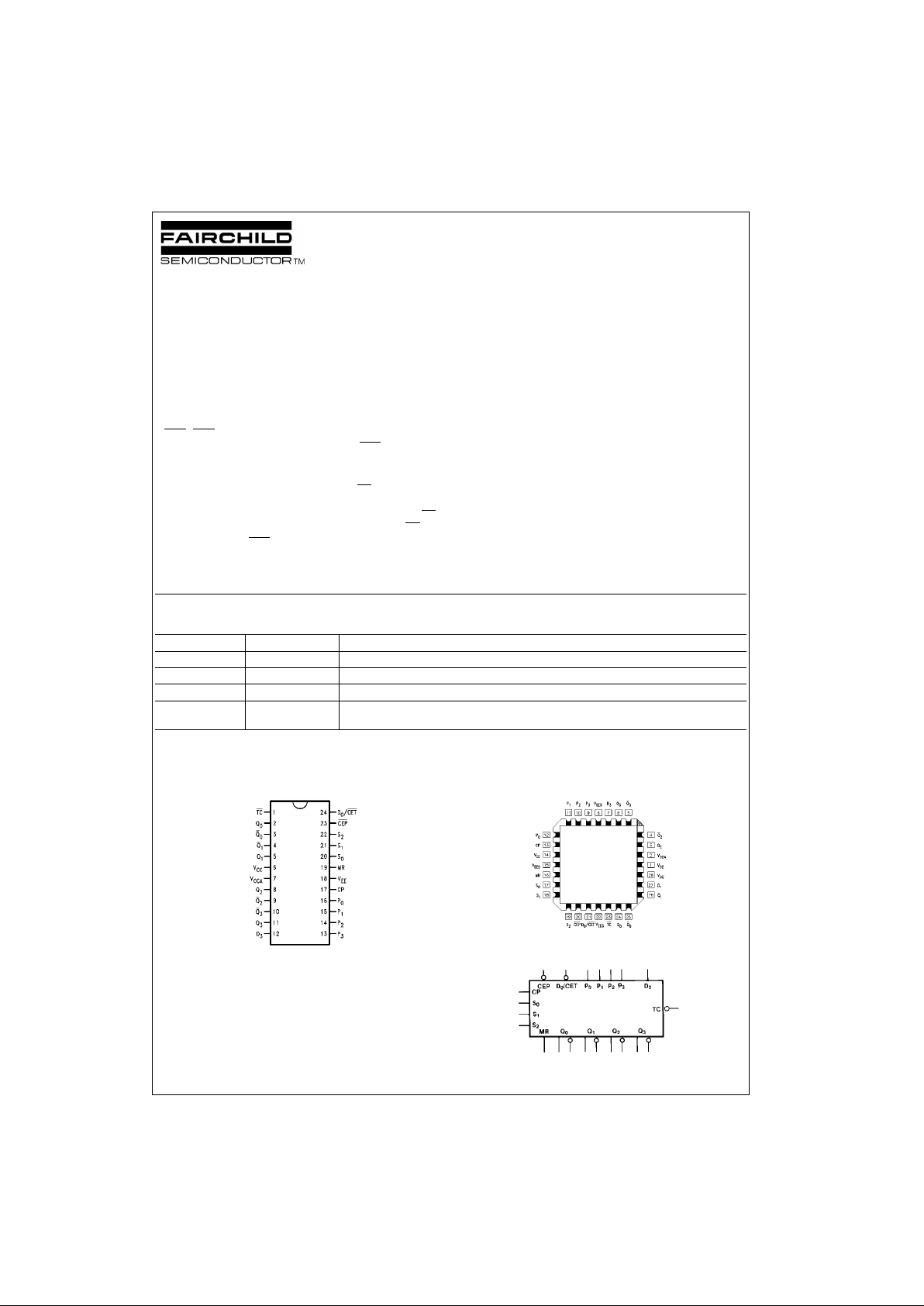
Connection Diagrams
24-Pin DIP/SOIC 28-Pin PLCC
Logic Symbol
Order Number Package Number Package Description
100336SC M24B 24-Lead Small Outline Integrated Circuit (SOIC), JEDEC MS-013, 0.300 Wide
100336PC N24E 24-Lead Plastic Dual-In-Line Package (PDIP), JEDEC MS-010, 0.400 Wide
100336QC V28A 28-Lead Plastic Lead Chip Carrier (PLCC), JEDEC MO-047, 0.450 Square
100336QI V28A 28-Lead Plastic Lead Chip Carrier (PLCC), JEDEC MO-047, 0.450 Square
Industrial Temperature Range (
−40°C to +85°C)

www.fairchildsemi.com 2
100336
Function Select Table Pin Descriptions
Truth Table
Q0 = LSB
1 = L if Q0–Q3 = LLLL
H if Q
0–Q3
≠ LLLL
2 = L if Q
0–Q3
= HHHH
H if Q
0–Q3
≠ HHHH
H = HIGH Voltage Level
L = LOW Voltage Level
X = Don't Care
= LOW-to-HIGH Transition
Note 1: Before the clock, TC
is Q
3
After the clock, TC is Q
2
S
2
S
1
S
0
Function
L L L Parallel Load
L L H Complement
L H L Shift Left
L H H Shift Right
H L L Count Down
HLHClear
H H L Count Up
HHHHold
Pin Names Description
CP Clock Pulse Input
CEP
Count Enable Parallel Input (Active LOW)
D
0
/CET Serial Data Input/Count Enable
Trickle Input (Active LOW)
S
0–S2
Select Inputs
MR Master Reset Input
P
0–P3
Preset Inputs
D
3
Serial Data Input
TC
Terminal Count Output
Q
0–Q3
Data Outputs
Q
0–Q3
Complementary Data Outputs
Inputs Outputs
MR S
2S1S0
CEP D0/CET D3CP Q3Q2Q1Q
0
TC Mode
LLLL X X X
P3P2P1P
0
L Preset (Parallel Load)
LLLHX X X
Q3Q2Q1Q
0
LInvert
LLHL X X X
D3Q3Q2Q
1
D
3
Shift to LSB
LLHH X X X
Q2Q1Q0D0Q3 (Note 1) Shift to MSB
LHLL L L X
(Q
0–3
) minus 1 1 Count Down
LHLL H L XXQ
3Q2Q1Q0
1 Count Down with CEP not active
LHLL X H XXQ
3Q2Q1Q0
H Count Down with CET not active
LHLHX X X
LLLL H Clear
LHHL L L X
(Q
0–3
) plus 1 2 Cou nt Up
LHHL H L XXQ
3Q2Q1Q0
2 Count Up with CEP not active
LHHL X H XXQ
3Q2Q1Q0
H Count Up with CET not active
L HHH X X X XQ
3Q2Q1Q0
HHold
HLLL X X XX LLL L L
HLLH X X XXLLLL L
HLHL X X XXLLLL L
H L H H X X X X L L L L L Asynchronous
H H L L X L X X L L L L L Master Reset
HHLL X H XXLLLL H
HHLH X X XXLLLL H
HHHL X X XXLLLL H
H HHH X X X X L L L L H

3 www.fairchildsemi.com
100336
Logic Diagram

www.fairchildsemi.com 4
100336
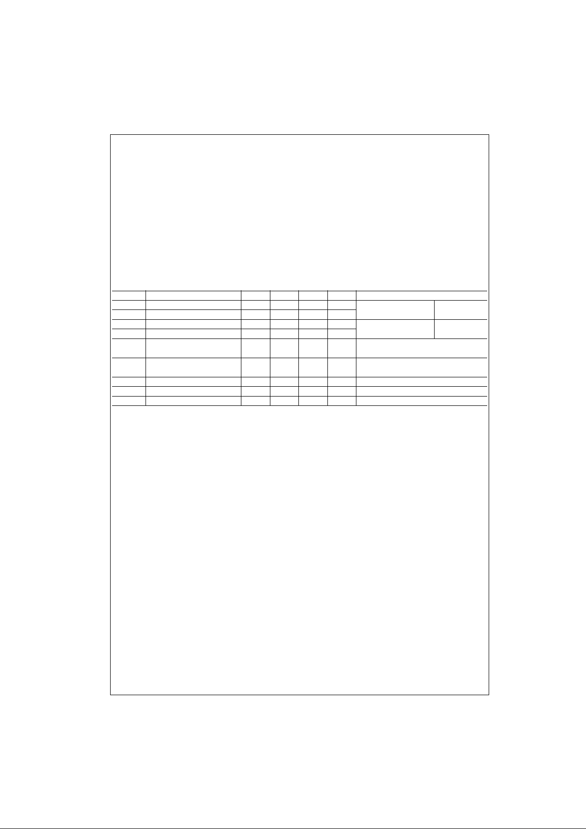
Absolute Maximum Ratings(Note 2) Recommended Operating
Conditions
Note 2: Absolute maximum ratings are those values beyond which the
device may be damaged or have its useful life impaired. Functional operation under these conditions is not implied.
Note 3: ESD testing conf orm s t o M I L-STD-883, Method 3015.
Commercial Version
DC Electrical Characteristics
(Note 4)
V
EE
= −4.2V to −5.7V, VCC = V
CCA
= GND, T
C
= 0°C to +85°C
Note 4: The specified limits represent the “worst case” value for the parameter. Since these values normally occur at the temperature extremes, additional
noise immunity and guardbanding can be achieved by decreasing the all owable syste m opera ti ng r ange s. Co ndi ti ons fo r t est ing shown in the ta ble s are chosen to guarantee operation under “worst case” conditions.
Storage Temperature (T
STG
) −65°C to +150°C
Maximum Junction Temperature (T
J
) +150°C
V
EE
Pin Potential to Ground Pin −7.0V to +0.5V
Input Voltage (DC) V
EE
to +0.5V
Output Current (DC Output HIGH)
−50 mA
ESD (Note 3)
≥ 2000V
Case Temperature (T
C
)
Commercial 0
°C to +85°C
Industrial
−40°C to +85°C
Supply Voltage (V
EE
) −5.7V to −4.2V
Symbol Parameter Min Typ Max Units Conditions
V
OH
Output HIGH Voltage −1025 −955 −870 mV VIN =V
IH (Max)
Loading with
V
OL
Output LOW Voltage −1830 −1705 −1620 mV or V
IL (Min)
50Ω to −2.0V
V
OHC
Output HIGH Voltage −1035 mV VIN = V
IH(Min)
Loading with
V
OLC
Output LOW Voltage −1610 mV or V
IL (Max)
50Ω to −2.0V
V
IH
Input HIGH Voltage −1165 −870 mV Guaranteed HIGH Signal
for All Inputs
V
IL
Input LOW Voltage −1830 −1475 mV Guaranteed LOW Signal
for All Inputs
I
IL
Input LOW Current 0.50 µAVIN = VIL (Min)
I
IH
Input HIGH Current 240 µAVIN = VIH (Max)
I
EE
Power Supply Current −165 −80 Inputs Open

5 www.fairchildsemi.com
100336
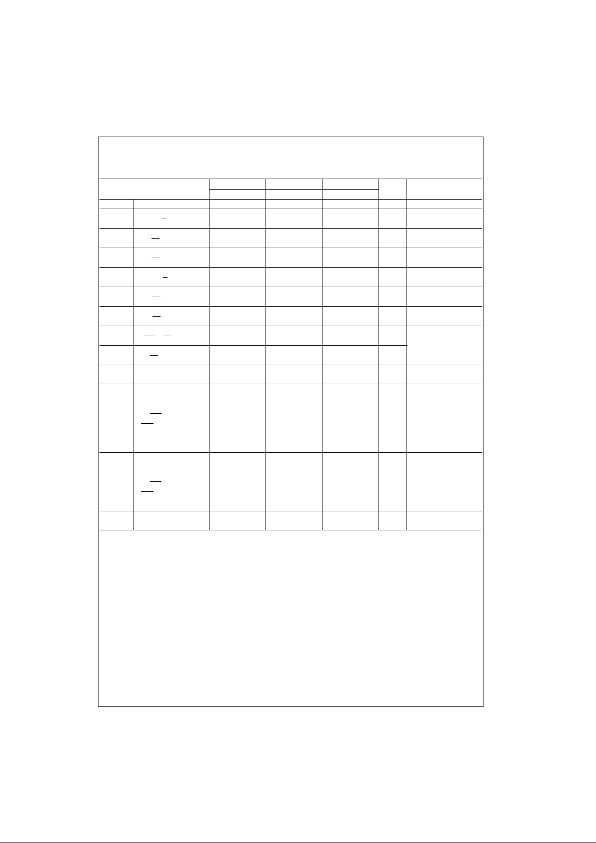
Commercial Version (Con tinu ed)
DIP AC Characteristics
V
EE
= −4.2V to −5.7V, VCC = V
CCA
= GND
Note 5: The propagation delay s pec ified is for single output swit c hing. Delays may vary up to 250 ps with multiple outpu ts s witching.
Symbol Parameter
TC = 0°CT
C
= +25°CT
C
= +85°C
Units Conditions
MinMaxMinMaxMinMax
f
SHIFT
Shift Frequency 300 300 300 MHz Figures 2, 3
t
PLH
Propagation Delay
1.00 2.00 1.00 2.00 1.00 2.00 ns
Figures 1, 3
t
PHL
CP to Qn, Q
n
(Note 5)
t
PLH
Propagation Delay
2.10 3.50 2.10 3.50 2.10 3.70 ns
Figures 1, 7, 8
t
PHL
CP to TC (Shift) (Note 5)
t
PLH
Propagation Delay
2.40 4.40 2.40 4.40 2.60 4.70 ns
Figures 1, 9
t
PHL
CP to TC (Count) (Note 5)
t
PLH
Propagation Delay
1.40 2.50 1.40 2.50 1.50 2.60 ns
Figures 1, 4
t
PHL
MR to Qn, Q
n
(Note 5)
t
PLH
Propagation Delay
2.80 5.10 2.90 5.20 3.10 5.50 ns
Figures 1, 12
t
PHL
MR to TC (Count) (Note 5)
t
PHL
Propagation Delay
2.40 4.00 2.40 4.00 2.50 4.10 ns
Figures 1, 10, 11
MR to TC (Shift) (Note 5)
t
PLH
Propagation Delay
1.80 3.10 1.80 3.10 1.90 3.30 ns
t
PHL
D0/CET to TC Figures 1, 5
t
PLH
Propagation Delay
1.90 4.10 1.90 4.10 2.10 4.40 ns
(Note 5)
t
PHL
Sn to TC
t
TLH
Transition Time
0.35 1.20 0.35 1.20 0.35 1.20 ns Figures 1, 3
t
THL
20% to 80%, 80% to 20%
t
S
Setup Time
D
3
1.00 1.00 1.00
P
n
1.50 1.50 1.50
D0/CET 1.30 1.30 1.30
ns Figures 6, 4
CEP 1.40 1.40 1.40
S
n
3.40 3.40 3.40
MR (Release Time) 2.60 2.60 2.60
t
H
Hold Time
D
3
0.40 0.40 0.40
P
n
0.30 0.30 0.30
ns Figure 6
D0/CET 0.30 0.30 0.30
CEP 0.20 0.20 0.20
S
n
0.10 0.10 0.10
tPW(H) Pulse Width HIGH
2.00 2.00 2.00 ns Figures 3, 4
CP, MR
 Loading...