

Page 1

LQ-510/AP-4000
TECHNICAL MANUAL
EPSON
Page 2

FCC COMPLIANCE STATEMENT
FOR AMERICAN USERS
This equipment uses and generates radio frequency energy and if not installed and used properly, that is,
in strict accordance with the manufacturer’s instructions, may cause interference to radio and television reception. It has been type tested and found to comply with limits for a Class B computing device in accordance
with Sub-part J of Part 15 of FCC Rules, which are designed to provide reasonable protection against such
interference in a residential installation. However, there is no guarantee that interference will not occur in
a particular installation. If this equipment does cause interference to radio or television reception, which can
be determined by turning the equipment on and off, the user is encouraged to try to correct the interference
by one or more of the following measures:
l reorient the receiving antenna
l relocate the computer with respect to the receiver
l move the computer away from the receiver
l plug the computer into a different outlet so that the computer and receiver are on different branch circuits.
If necessary, the user should consult the dealer or an experienced radio/television technician for additional
suggestions. The user may find the following booklet, prepared by the Federal Communications Commission, helpful: “ How to Identify and Resolve Radio-TV Interference Problems.
the U.S. Government Printing Office, Washington, D.C., 20402, Stock No. 004-000-00345-4.
© 1989 Seiko Epson Corporation
” This booklet is available from
Epson America, Inc.
Customer Service Department
23610 Telo Avenue
Torrance, California 90505
All rights reserved. No portion of this document may be reproduced, stored in a retrieval system, or transmit-
ted in any form or by any means, electric, mechanical, photocopying, recording, or otherwise, without the
written permission of Epson America, Inc. No patent liability is assumed with respect to use of the informa-
tion contained herein. While every precaution has been taken in the preparation of this book, Epson America,
Inc., assumes no responsibility for errors or omissions. Neither is any liability assumed for damages resulting
from the use of the information contained herein.
Epson@
is a registered trademark of Seiko Epson Corporation.
LQ-510TM is a trademark of Epson America, Inc.
ii
LQ-510
Page 3

REV.-A
Precautionary notations throughout the text are categorized relative to 1) personal injury, and 2) damage
to equipment:
DANGER
Signals a precaution which, if ignored, could result in serious or fatal personal in-
jury. Great caution should be exercised in performing procedures preceded by a
DANGER heading.
WARNING
Signals a precaution which, if ignored, could result in damage to equipment.
The precautionary measures itemized below should always be observed when performing repair/maintenance
procedures.
DANGER
1. ALWAYS DISCONNECT THE PRODUCT FROM BOTH THE POWER SOURCE AND
PERIPHERAL DEVlCES BEFORE PERFORMING ANY MAINTENANCE OR REPAIR
PROCEDURE.
2. NO WORK SHOULD BE PERFORMED ON THE UNIT BY PERSONS UNFAMILIAR WITH
BASIC SAFETY MEASURES AS DICTATED FOR ALL ELECTRONICS TECHNICIANS IN
THEIR LINE OF WORK.
3. WHEN PERFORMING TESTING AS DICTATED WITHIN THIS MANUAL, DO NOT CONNECT THE UNIT TO A POWER SOURCE UNTIL INSTRUCTED TO DO SO. WHEN THE
POWER SUPPLY CABLE MUST BE CONNECTED, USE EXTREME CAUTION IN WORKING ON POWER SUPPLY AND OTHER ELECTRONIC COMPONENTS.
WARNING
1. Repairs on Epson products should be performed on/y by an Epson-certified repair
technician.
2. Make certain that the source voltage is the same as the rated voltage, listed on the serial
number/rating plate. If the Epson product has a primary AC rating different from the
available power source, do not connect it to the power source.
3. Always verify that the Epson product has been disconnected from the power source before
removing or replacing printed circuit boards and/or individual chips.
4. In order to protect sensitive microprocessors and circuitry, use static discharge equipment, such as anti-static wrist straps, when accessing internal components.
5. Replace malfunctioning components only with those components recommended by the
manufacturer; introduction of second-source ICs or other nonapproved components may
damage the product and void any applicable Epson warranty.
LQ-510
-iii-
Page 4
REVISION SHEET
REV-A
-iv-
LQ-510
Page 5

FCC Compliance Statement for American Users
This equipment has been tested and found to comply with limits for a Class B digital device,
pursuant to Part 16 of the FCC Rules. These limits are designed to provide reasonable protections
against harmful interference in a residential installation. This
radiate radio frequency energy and, if not installed and used in accordance with the instructions,
may cause harmful interference to radio or television reception, which can be determined by turning
the equipment off and on. The user is encouraged to try to correct the interference by one or more of
the following measures:
l
Reorient or relocate the receiving antenna
l
Increase the separation between the equipment and the receiver
l
Connect
connected
l
Consult the dealer or an experienced radio/TV technician for help.
the equipment to an outlet on a circuit different from that to which the receiver is
WARNING: The connection of a nonshielded interface cable to this equipment will
invalidate the FCC Certification of this device and may cause interference levels that
exceed the limits established by the FCC for this equipment. If this equipment has more
than one interface connector, do not leave cables connected to unused interfaces.
For Canadian Users
This digital apparatus does not exceed the Class B limits for radio noise emissions from digital
apparatus as set out in the radio interference regulations of the Canadian Department of
Communications.
equipment
generates, uses, and can
Le p&sent appareil
applicable6 aux
radio&ctriques
num&ique n’emet
appareils
act4
numeriques
par le Ministire des Communications du Canada.
pas de bruits radio&ctxiques
de Classe B
prescrites
dans le
dbpassant
reglement
les
limites
sur le brouillage
Subsequent product modifications will be brought to your attention via service bulletins. Please
revise the text when you receive these bulletins.
This document is subject to change without notice.
All rights reserved. No part of this publication may be reproduced, stored in
a
retrieval system, or
transmitted in any form or by any means, mechanical, photocopying, recording, or otherwise,
without the prior written permission of Epson America, Inc. No patent liability is assumed with
respect to use of the information contained herein. While every precaution has been taken in the
preparation of this book, Epson America, Inc., assumes no responsibility for errors or omissions.
Neither is any liability assumed for damages resulting from the use of the information contained
herein.
e 1990 Epson America, Inc.
Epson America, Inc.
23610 Telo Avenue
Torrance,
California 90505
Epson is a registered trademark of Seiko Epson Corporation
ActionPrinter is a trademark of Epson America, Inc.
ActionPrinter 4000
Page 6
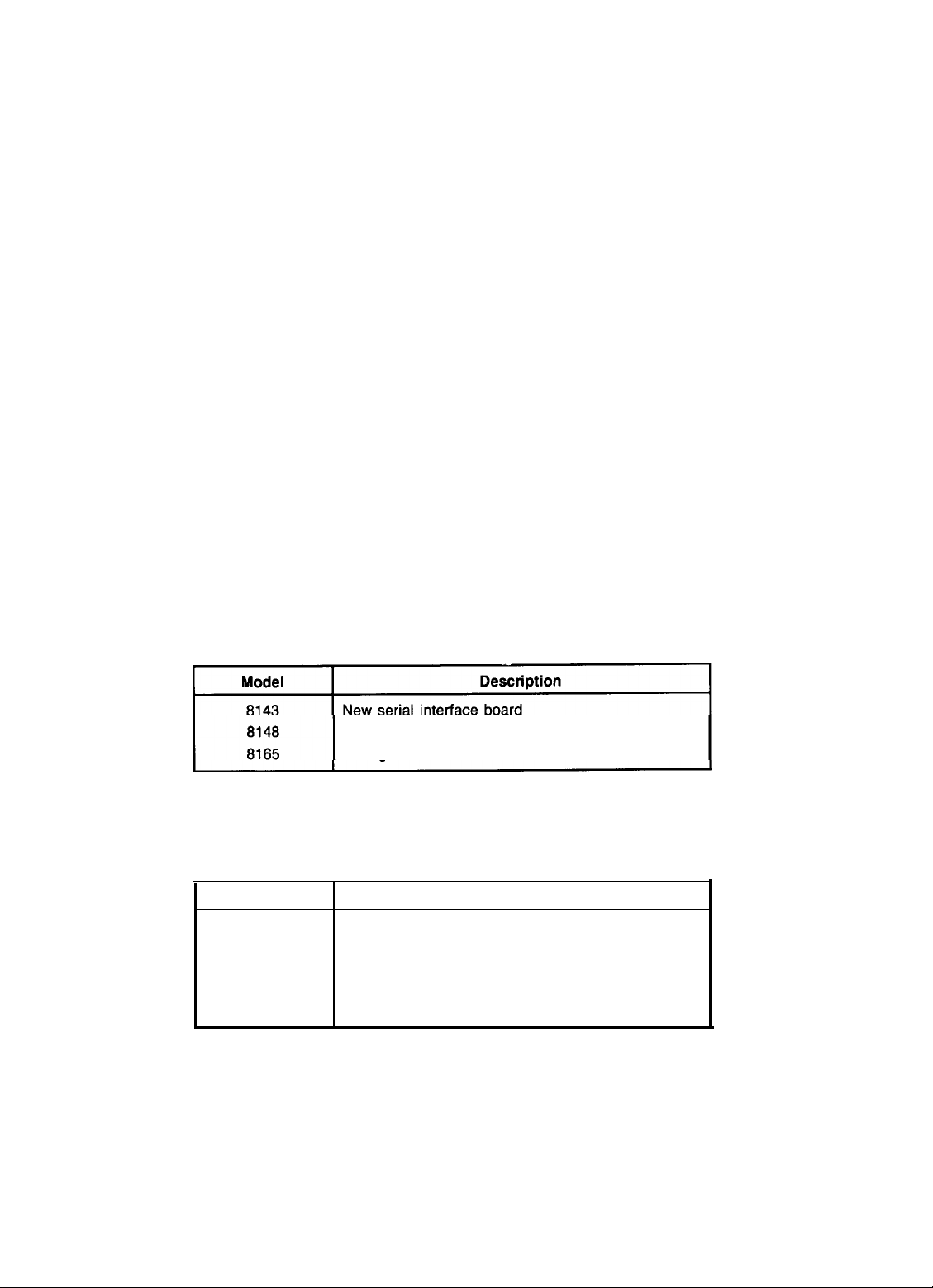
Addendum
The AP4000 is mechanically and electronically the same
as the LQ-510.
All the information contained herein is equally
applicable to both printers.
Below is a list of unique parts for the Epson ActionPrinter 4000:
Part Number
ActionPrinter 4000 parts not listed above are identical to those for the LQ-510.
Description
Logo plate
Individual carton box
Pad sleeve
Page 7

REV.-A
TABLE OF CONTENTS
CHAPTER 1.
CHAPTER 2.
CHAPTER 3.
CHAPTER 4.
CHAPTER 5.
CHAPTER 6.
APPENDIX
GENERAL DESCRIPTION
PRINCIPLES OF OPERATION
OPTIONAL EQUIPMENT
DISASSEMBLY, ASSEMBLY, AND ADJUSTMENT
TROUBLESHOOTING
MAINTENANCE
LQ-510
vi
Page 8

REV.-A
GENERAL DESCRIPTION
CHAPTER 1
GENERAL DESCRIPTION
1.1
FEATURES
1.2
SPECIFICATIONS
1.2.1 Hardware Specifications
1.2.2 Firmware Specifications (ESC/P)
INTERFACE OVERVIEW
1.3
1.4
DIP SWITCHES AND JUMPER SETTING
1.4.1 DIP Switch Settings
1.4.2 Jumper Setting
SELECTYPE FUNCTION
1.5
1.6
SHEET LOADING AND SHEET EJECTION
TEAR-OFF FUNCTION
1.7
OPERATING INSTRUCTIONS
1.8
1.8.1 Self-Test.............................................................................
1.8.2 Hexadecimal Dump Function
1.8.3 Bit-Image Printing
1.8.4 Error Conditions
1.8.5 Buzzer Operation
1.8.6 Printer Initialization
1.8.7 Default Values
1.8.8 Adjust Lever Operation
1.8.9 Printer Protection for Heavy-Duty Printing
1.9
MAIN COMPONENTS
1.9.1 SAMA Board .......................................................................
1.9.2 SANPNL Control Panel
1.9.3 SANPS(E) Board
1.9.4 Printer Mechanism (M-5710)
1.9.5 Housing..............................................................................
....................................................................................
...........................................................................
..................................................................
.............................................................
...................................................................
..................................................................
....................................................................
...........................................................
...............................................................
..................................................................
................................................................
.............................................................
....................................................................
........................................................
......................................................................
........................................................
..................................................................
......................................................
..........................................
...........................................
.........................................
................................................
...............................
.................................................
1-1
1-3
1-3
1-9
1-13
1-16
1-16
1-17
1-17
1-18
1-18
1-19
1-19
1-20
1-21
1-22
1-22
1-22
1-23
1-23
1-24
1-25
1-26
1-27
1-28
1-28
1-29
LQ-510
1-i
Page 9

GENERAL DESCRIPTION
REV.-A
LIST OF FIGURES
Figure 1-1. Exterior Views of the LQ-510
Figure 1-2. Pin Configuration
Figure 1-3. Label Dimensions
Figure 1-4.
Figure 1-5.
Figure 1-6. Character Matrix
Figure 1-7. Data Transmission Timing
Figure 1-8.
Figure 1-9. Hexadecimal Dump Function
Figure 1-10.
Figure 1-11.
Figure 1-12. SAMA Main Control Board
Figure 1-13.
Figure 1-14. Power Supply Filter Board
Figure 1-15. Model 5710 Printer Mechanism
Figure 1-16. Housing
Printable Area for Cut Sheets
Printable Area for Continuous Paper
Self-Test Printout
Lever Position
LQ-510 Component Layout
SANPNL Control Panel
..........................................................................
............................................................
............................................................
..............................................................
............................................................
.................................................................
............................................
...........................................
................................................
............................................
...............................................
...............................................
....................................................
...............................................
.........................................
LIST OF TABLES
.................................
1-2
1-3
1-5
1-6
1-7
1-12
1-13
1-19
1-20
1-23
1-25
1-26
1-27
1-26
1-28
1-29
Table 1-1. Interface Options
Table 1-2. Optional Units
Table 1-3. Cut-Sheet Specifications
Table 1-4.
Table 1-5.
Table 1-6.
Table 1-7. Printing Mode
Table 1-8.
Table 1-9.
Table 1-10.
Table 1-11.
Table 1-12.
Table 1-13.
Table 1-14.
Table 1-15. Character
Table 1-16.
Table 1-17.
Table 1-18.
Continuous Paper Specifications
Envelope Specifications
Label Specifications
Character Matrix and Character Size
Data Transmission Timing
Printer Select/Deselect Control
Settings for DIP Switch 1 (SW1)
Settings for DIP Switch 2 (SW2)
International Character Set Selection
Font Selection
Pitch
Print
Density..
Bit-Image Printing
Lever Position
.............................................................
.................................................................
..................................................
...................................................
.........................................................
..................................................................
.................................................................
Selection..
.................................................................
............................................................
.................................................................
......................................
................................
................................................
........................................
.......................................
.......................................
................................
...............................................
1-1
1-1
1-4
1-4
1-5
1-5
1-10
1-11
1-13
1-15
1-16
1-16
1-16
1-17
1-17
1-21
1-21
1-23
1 -ii
LQ-510
Page 10
REV.-A
GENERAL DESCRIPTION 1
1.1 FEATURES
The LQ-510 is a small, light-weight, low-cost printer, comparable to the LQ-500 with advanced paper-handling.
Its main features are as follows:
1. Advanced paper handling: auto back-out and cut-sheet loading.
2.
Expanded ESC/P-code printing, implemented as a standard feature.
3.
Printing speeds in characters per second (cps):
4. Optional 8100 series interface.
5.
Clear, easy-to-read printing with a standard Epson font.
6. Two built-in LQ fonts (Roman and Sans Serif).
7.
An optional multi-font module can provide a wide variety of fonts.
8.
Control panel switch selection of Draft, Roman, Sans Serif, or slot-mounted (optional multi-font module)
font.
9.
Control panel switch selection of normal or condensed printing.
10. Optional cut-sheet feeder (CSF) for easy handling of cut sheets.
180 cps (alphanumeric Draft 12 cpi)
150 cps (alphanumeric Draft 10 cpi)
60 cps (alphanumeric LQ 12 cpi)
50 cps (alphanumeric LQ 10 cpi)
The LQ-510 is equipped with the standard Epson 8-bit parallel interface. Various interface options allow printing from a wide variety of computers, Table l-l lists the interface options, Table 1-2 lists the optional units
available, and Figure l-l shows an exterior view of the printer.
Table l-l. Interface Options
Intelligent serial interface board
Intelligent IEEE-488 interface board
NOTE:
Refer to the “Optional Interface Technical Manual” for details.
Table 1-2. Optional Units
Model
C80612
C80006
7753
7768
7407
Single-bin cut-sheet feeder
Pull tractor unit
Ribbon cartridge (black)
Film ribbon cartridge
Multi-font cartridge
Description
LQ-510
1-1
Page 11
GENERAL DESCRIPTION
REV.-A
(Printer Cover A)
(Printer Cover B)
1-2
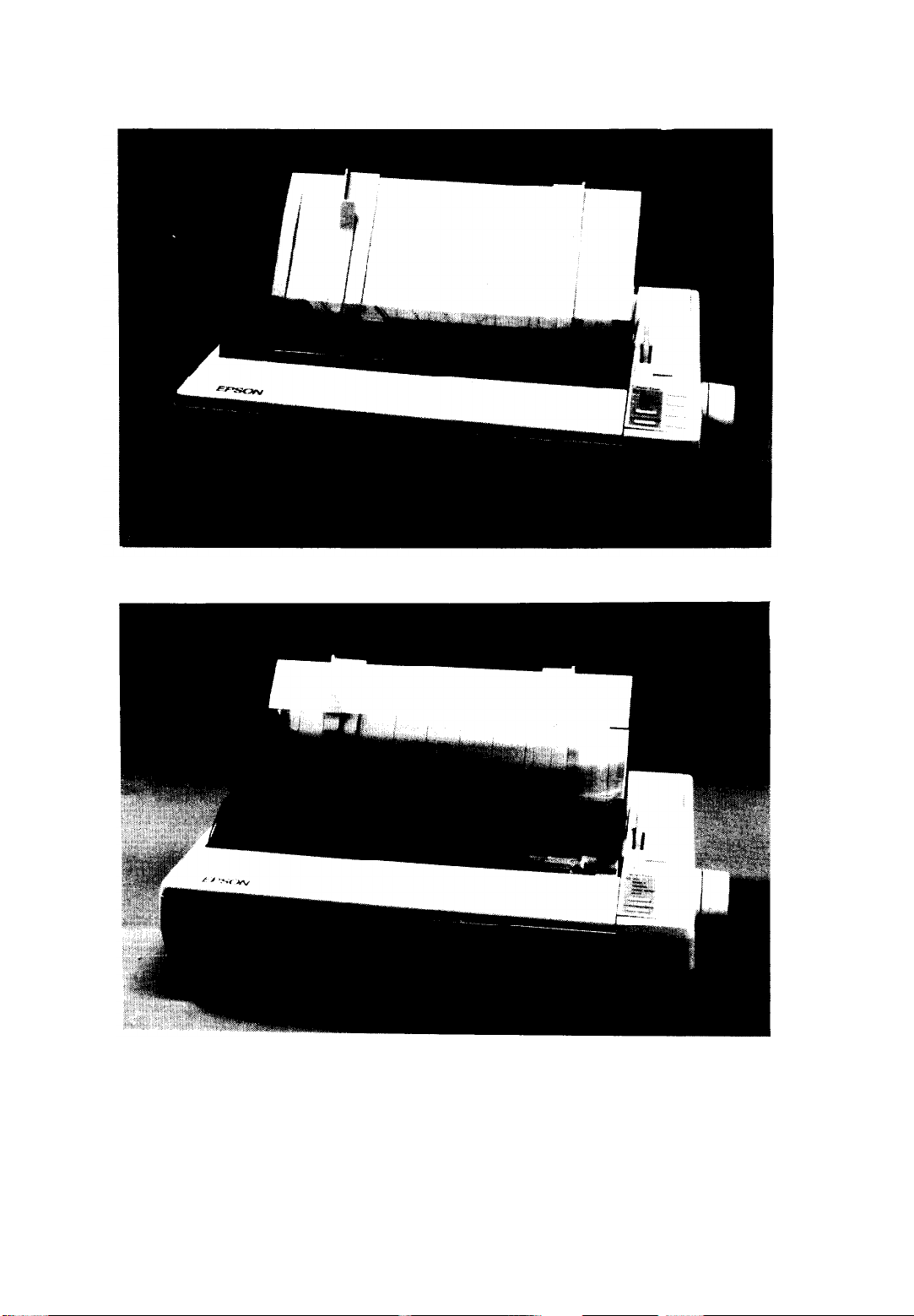
Figure l-l. Exterior Views of the LQ-510
LQ-510
Page 12
REV.-A
1.2 SPECIFICATIONS
This section describes the specifications for the LQ-510 printer.
1.2.1 HARDWARE SPECIFICATIONS
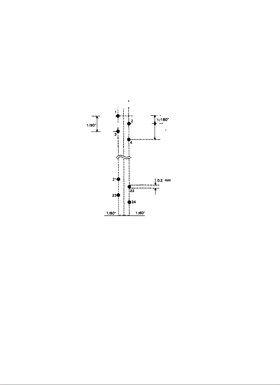
GENERAL DESCRIPTION
Printing Method
Pin Configuration
Serial, impact, dot matrix
24 wires (12 x 2, staggered, 0.2 mm diameter)
Wires
-
-----
lf90"
_I
(Column 1) Wires (Column 2)
-----
II
I .
I
.t;
l+j-
I
+
' i
8i
+----A-
/ i
I
I .
II
II
II
I
------ --
-------
I
I
i
11190"
_-
1190"
Figure 1-2. Pin Configuration
Feeding Method
NOTE:
Be aware of the following points regarding paper handling.
Friction feed, tractor feed (push tractor: standard; pull tractor: optional)
Friction Feed:
1.
Do not use continuous paper.
2.
Do not use a single sheet shorter than 7.28 inches (182 mm) or longer than 10.28 inches (257 mm).
3.
Do not perform a reverse paper feed when the paper is within .34 inch (8.5 mm) from the top or within
.88 inch (22 mm) from the bottom.
4.
Do not perform a reverse feed greater than 1/6 inch after the paper end has been detected.
5. Use the pull-out unit.
6. Do not use multi-part single-sheet forms.
Tractor Feed
1. Release the friction-feed mechanism.
2.
Multiple copies must be joined by pasting at the perforation or tractor holes.
3.
Paper for copies must be carbonless, multi-part paper.
LQ-510
1-3
Page 13

GENERAL DESCRIPTION
REV.-A
Push Tractor Feed
1. Use the pull-out unit.
2.
Do not perform reverse feeding for distances greater than 1/6 inch.
3.
Accuracy of paper feed cannot be assured, and reverse feeding cannot be performed, after the paper
end is detected.
Push-Pull Feed
1.
Remove the pull-out unit and attach the pull tractor unit.
2.
Do not lose the paper between the platen and pull tractor unit.
3.
Precisely adjust the horizontal positions of the pull and the push tractors.
4.
Do not perform reverse feeding for distances greater than 1/6 inch.
5.
Do not perform reverse feeding after the paper end is detected.
Pull Tractor Feed
1.
Remove the pull-out unit and attach the pull tractor unit.
Line Spacing
Paper Insertion
Paper-Feed Speed
Paper Specifications
Width
Length
Thickness
Weight
Quality
Copies
1/6 inch, or programmable in units of 1/360 inch
From rear
Friction, without CSF
100 ms/line (at 1/6-inch line feed)
2.2 inches per second (continuous feed)
Friction, with CSF
100 ms/line (at 1/6-inch line feed)
2.2 inches per second (continuous feed)
Tractor
100 ms/line (at 1/6-inch line feed)
2.2 inches per second (continuous feed)
See Tables 1-3 through 1-6.
Table 1-3. Cut-Sheet Specifications
7.15 to 10.1 inches (182 to 257 mm)
14.3 inches, maximum (364 mm, maximum)
0.0025 to 0.0055 inch (0.065 to 0.14 mm)
14 to 24 pounds (52.3 g/m2 to 90 g/m2)
Xerographic, bond, airmail paper, etc.
Not available
Table 1-4. Continuous-Paper Specifications
1-4
Width
Copies
Quality
Total Thickness
Weight
4 to 10 inches (101 to 254 mm)
3 sheets (1 original and 2 copies)
Bond, xerographic, airmail, etc.
0.0025 to 0.01 inch (0.065 to 0.25 mm)
1 sheet - 14 to 22 pounds (52.3 g/m2 to 82 g/m2)
3 sheets - 12 to 15 pounds (40 g/m2 to 58.2 g/m2) each
LQ-510
Page 14
REV.-A
GENERAL DESCRIPTION
Table 1-5. Envelope Specifications
Size
Quality
Thickness
Number 6: 6.64 x 3.68 inches (166 x 92 mm)
Number 10: 9.6 x 4.16 inches (240 x 104 mm)
Bond paper, xerographic paper, airmail
0.0063 to 0.0197 inch (0.16 to 0.52 mm)
(Within the printing area, the thickness differential must not exceed 0.0098 inch [0.25
mm]).)
12 to 24 pounds (45 g/m2 to 91 g/m2)
NOTES:
1. Printing on envelopes can be performed only when the temperature is normal.
2. Envelopes should be positioned horizontally.
3. For Number 6 envelopes, set the left side so that it matches the setting mark on the sheet guide.
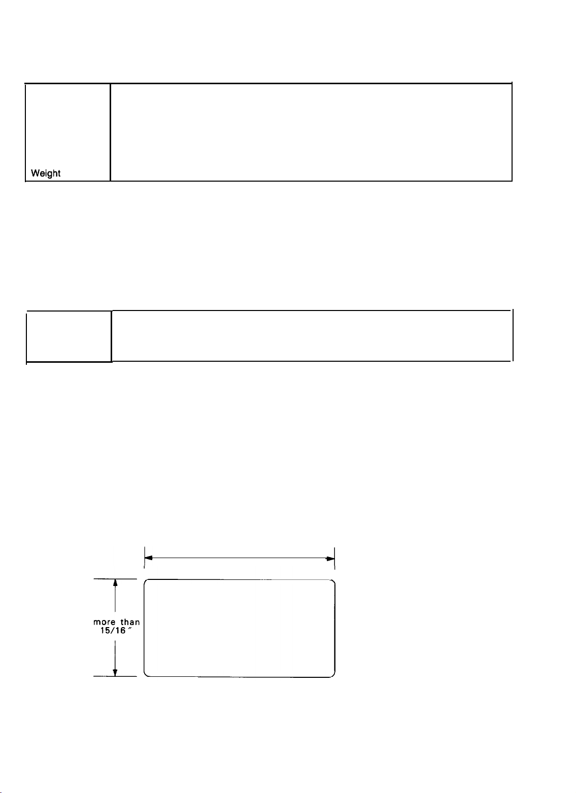
Table 1-6. Label Specifications
Sire
Thickness
Greater than 2½ x 15/16 inches (63.5 x 23.8 mm)
0.0063 to 0.0075 inch (0.16 to 0.19 mm)
*Thickness of the base paper must be 0.0028 to 0.0031 inch (0.07 to 0.09 mm)
NOTES:
1. Printing on labels is available only at normal temperatures.
2. Labels must be fanfold.
3. For printing on labels with pressure sensitive paper, the following conditions must be met:
(1)
sheets of labels must be joined at the perforation or tractor holes.
(2) the total thickness may not be greater than 0.0118 inch (0.3 mm)
(3) the temperature must be between + 41 °F and + 95 °F (+ 5° and + 35°C), and relative humidity
between 10% and 80%
4. Examples of acceptable labels: Avery Continuous-Form Labels
Avery Mini-Line Labels
5. Do not perform reverse feed.
more than 2 1/2 "
\
/
R : more than 2.5 mm
LQ-510
Figure 1-3. Label Dimensions
1-5
Page 15
GENERAL DESCRIPTION
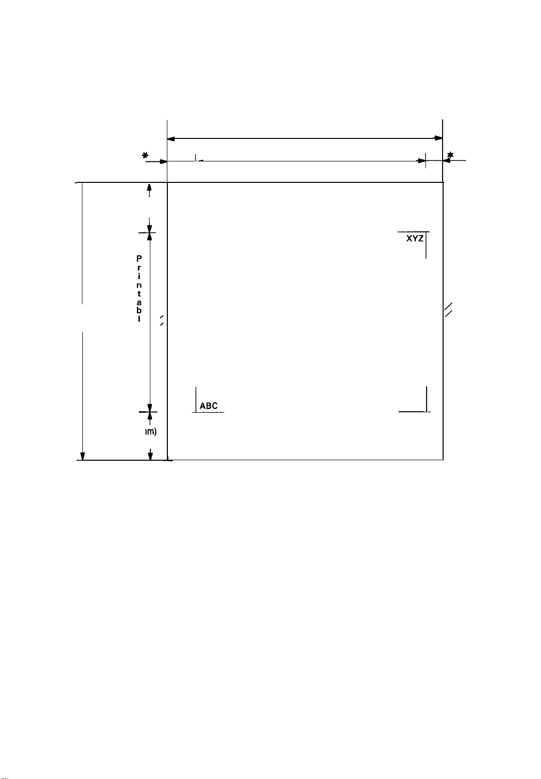
Printable Area
The figure below illustrates the printable area for cut sheets.
7.2-10.1 ” (182-257mm)
I
REV.-A
*
.33” (8.5
or more
14.3” (364 mm),
maximum
.53” (13.5 m
or more
*
mm)
-
7
e
a
r
e
a
-
I-
t
ABC
›r
,
/
/
ABC
L
Printable area
I
XYZ
XYZ
1
Figure 1-4. Printable Area for Cut Sheets
* At least 0.12 inch (3 mm) when paper width is less than 9 inches (229 mm); at least .9 inch (24 mm) when
the paper width is 10.1 inches (257 mm).
Printing is possible approximately 1.12 inches (28 mm) from the paper’s detected bottom edge; the .53 inch
(13.5 mm) value (lowest print position) is for reference only. Paper feed accuracy cannot be assured within
0.87 inch (22 mm) of either the top or bottom edge.
1-6
LQ-510
Page 16
REV.-A
GENERAL DESCRIPTION
Printable
area
--t
9 mm, 0.35"
or more
9 mm ,0.35”
t
or more
Printable
area
4
*1)
0
0
0
0
0
0
0
0
0
0
0
0
0
0
0
0
0
4.0" -10.0",
I_
I_
101 mm-254 mm
Printable area
_I
*2)
I
m
0
0
0
0
0
0
0
i-
ABC
XYZ
-I
0
0
0
0
---------
0
0
0
0
0
ABC
0
+
0
0
0
0
0
0
XYZ
0
0
t
0
0
0
0
0
0
*
NOTES:
LQ-510
Figure 1-5. Printable Area for Continuous Paper
1. .52 inch (13 mm) or greater for paper widths of 4 to 9.5 inches (101 to 242 mm).
1.04 inches (26 mm) or greater for paper widths of 10 inches (254 mm).
2. .52 inch (13 mm) or greater for paper widths of 4 to 9.5 inches (101 to 242 mm).
.96 inch (24 mm) or greater for paper widths of 10 inches (254 mm).
1-7
Page 17

GENERAL DESCRIPTION
Ink Ribbon
REV.-A
Fabric
Film
Reliability
Printhead Life
Safety Approvals
Safety Standards
Radio Frequency
Interference (RFI)
Model: 7753 ribbon cartridge
Color: black
Reliability: 2 million (LQ characters at 48 dots/character)
Dimensions:
Model: 7768 ribbon cartridge
Color: black
Reliability: 2
Dimensions:
Mean Cycles Between Failures (MCBF): 3 million lines (excluding
printhead)
Mean Time Before Failure (MTBF): 4000 Power-On Hours (25% duty)
200 million strokes/wire
UL478 (U.S. version)
CSA22.2#154
VDE0806 (TUV) (European version)
FCC class B (U.S. version)
VDE0871 (self-certification) (European version)
11.6 (width) x 1.36 (height) x 2.84 (depth)
(290 mm x 34 mm x 71 mm)
million characters at 48 dots/character
11.6 (width) x 1.36 (height) x 2.84 (depth)
(290 mm x 34 mm x 71 mm)
inches
inches
Electrical Specifications
Power Conditions
Frequency Range
Rating Current
Insulation Resistance
Dielectric Strength
Environmental Requirements
Temperature
Humidity
Shock Resistance
Resistance to Vibration
Physical Specifications
Weight
Dimensions
108 VAC to 132 VAC (120 V version)
198 VAC to 264 VAC (220/240 V version)
49.5 to 60.5 Hz
1.8 A AC (120 V version)
1 A AC (220/240 V version)
10 megohms minimum (between AC line and chassis)
1250 VAC (rms), 1 minute (120 V version) (between AC line and
chassis)
3750 VAC (rms), 1 minute (220/240 V version)
41° to 95°F (5 to 35°C) - operating
-22° to 140° F (-30 to 60° C) - with shipment container
10 to 80% RH - operating
5 to 85% RH
1 G, within 1 ms - operating
2 G, within 1 ms - non-operating
0.25 G, 55 Hz maximum - operating
0.50 G, 55 Hz maximum - storage
13.23 pounds (6 kg)
16.72 (width) x 13.88 (depth) x 5.6 (height) inches
(418 x 347 x 139.9 mm), excluding knobs and paper guides
- non-operating
1-8
LQ-510
Page 18

REV.-A
1.2.2 FIRMWARE SPECIFICATIONS (ESC/P)
GENERAL DESCRIPTION
Control Codes
Printing Direction
Input Data Buffer
Character Code
Character Sets
Family
Font
Printing Mode
Printing Speed
Printing Columns
Character Matrix
Character Size
ESC/P-84 (Epson Standard Code for Printers)
Bidirectional (text)
Bidirectional (bit-image) (when SW 2-6 is ON and control command [ESC
U 1] input)
Unidirectional (bit-image)
8K bytes (when SW 2-5 is ON)*
1K byte (when SW 2-5 is OFF)
* If DIP SW 2-5 is set to ON, downloading will be ignored.
8-bit
96-character ASCII and 15 international character sets
Epson Roman (Family number: 0)
Epson Sans Serif (Family number: 1)
Epson Roman 10, Epson Roman 12, Epson Roman 15,
Epson Roman Proportional
Epson Sans Serif 10, Epson Sans Serif 12,
Epson Sans Serif 15, Epson Sans Serif Proportional
Epson Draft 10, Epson Draft 12, Epson Draft 15
Selection and mixing of the following modes are allowed (except that 15 cpi
Condensed Mode is not available):
l
Printing quality (draft/letter quality)
0 Character pitch (10, 12, 15, or proportional)
0 Condensed
0 Double-width
0 Double-height
0
Bold
0 Double-strike
0
Italic
0 Underlined
0 Double-underlined
0 Overscore
0 Strike-through
0
Outline
0 Shadow
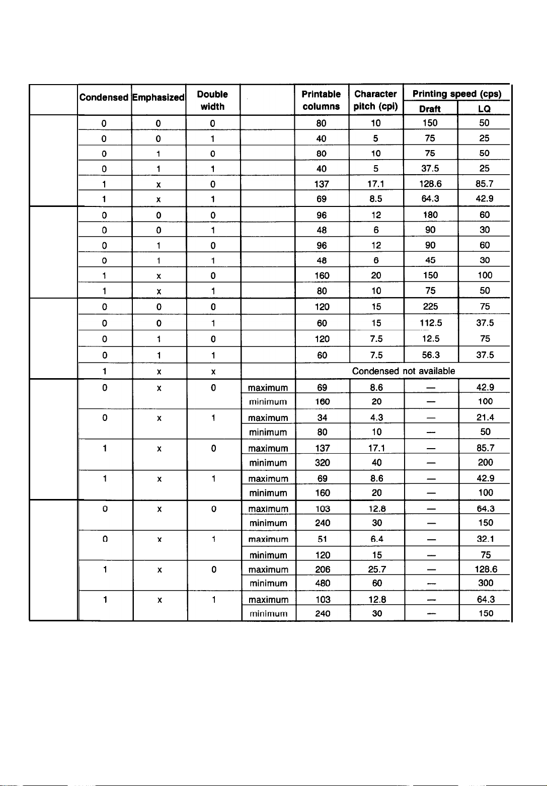
See Table 1-7.
See Table 1-7.
See Table 1-8.
See Table 1-8.
LQ-510
1-9
Page 19
GENERAL DESCRIPTION
Print
pitch
10
12
15
REV.-A
Table 1-7. Printing Mode
Pro-
portional
Pro-
portional
super/
subscript
NOTES:
1. The
2. The
“maximum”
“minimum”
value applies when only characters of maximum width are printed.
value applies when only characters of minimum width are printed.
3. “-” indicates that the “LQ” character set is automatically selected when proportional pitch
is specified.
1-10
LQ-510
Page 20
REV.-A
GENERAL DESCRIPTION
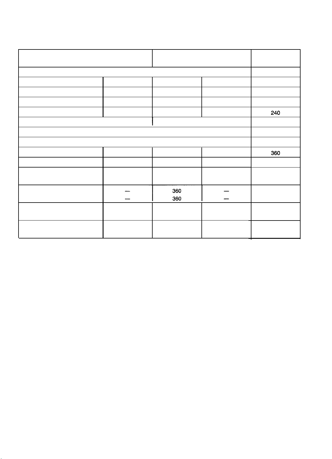
Table 1-8. Character Matrix and Character Size
Printing mode
Draft
10-pitch
Draft 12-pitch
Draft
15-pitch
Draft 10-pitch,
Draft
12-pitch.
LQ 10-pitch
LQ 12-pitch
LQ 15-pitch
LQ
10-pitch, condensed
LQ
12-pitch, condensed
LQ
proportional
LQ proportional, condensed
LQ
proportional, super/
subscript
LQ
proportional,
subscript, condensed
condensed
condensed
super/
Face matrix
I
9 x 23
I
9
x 23
9
X 16
29 x 23
I
29 x 23
I
15 x 16
I
37x23
18
x 23 minimum
28x16
12x16
-
-
-
-
maximum
maximum
minimum
-
-
HDD
I
I
I
I
120
120 1.9x3.2
120
240
240
360
360
360
360
360
360 2.6
360
360
360
360
360
Character size
H x V (mm)
I
1.9 x 3.2
I
1.0x2.3
-
-
2.0 x 3.2
I
2.0 x 3.2
I
1.0 x 2.3
I
-
x 3.2
1.Ox3.2
1.8 x 2.3
0.7 x
2.3
-
-
Unit ESC sp
120
120
120
240
180
180
180
360
180
180
360
360
180
180
360
360
NOTES: 1.HDD is horizontal dot density in dots per inch.
2.
Face matrix and character size indicate maximum character size. This value changes according to differences in paper, ribbon, etc.
3.
Unit ESC sp (which also can be sent as the unit followed by the character string CHR$(&h20))
indicates the minimum length to be added to the right of the character that can be specified
with the ESC sp control code.
4. “_”
indicates that character matrix is reshaped by printer firmware. Character width becomes
half of noncondensed character width.
LQ-510
1-11
Page 21
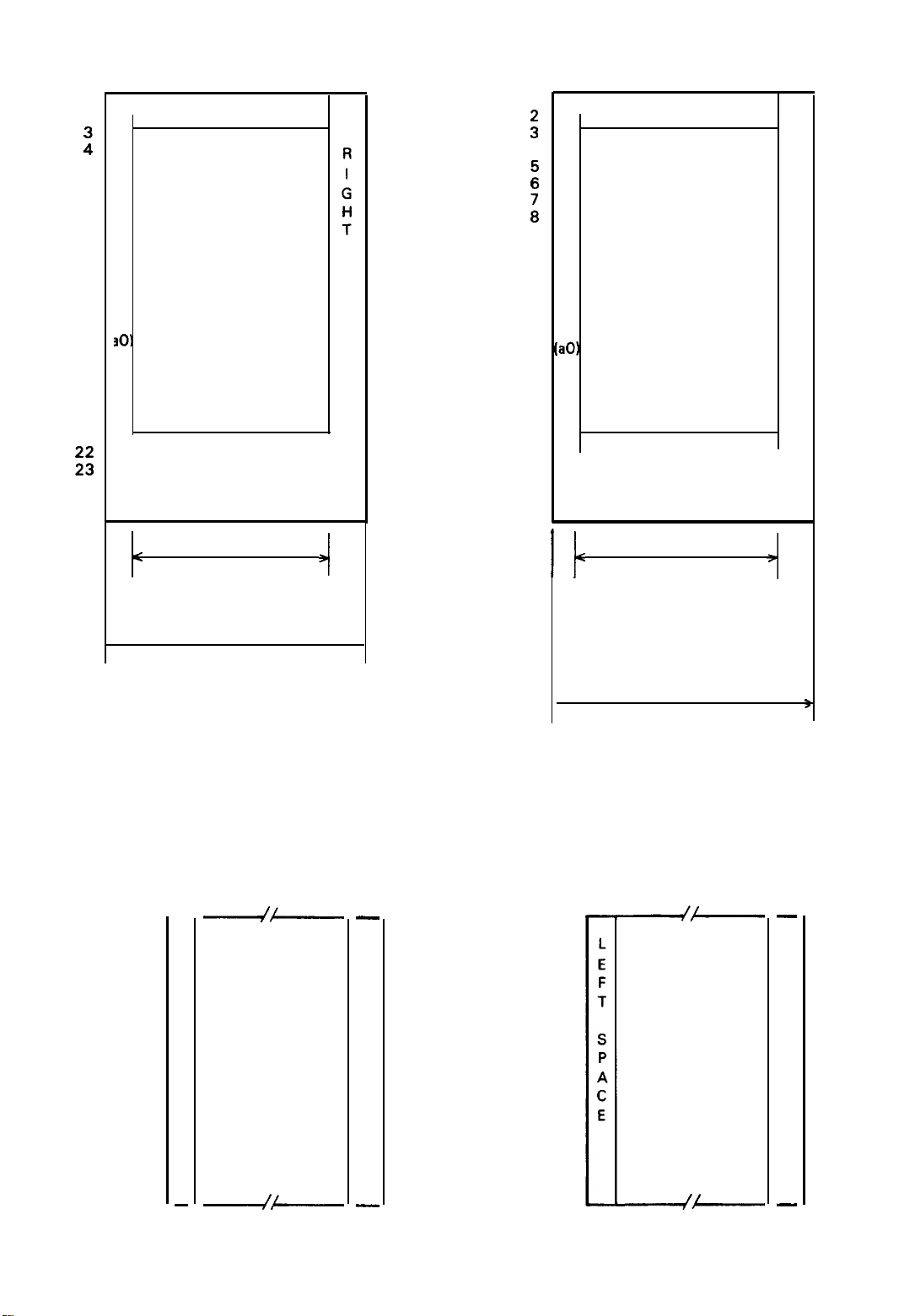
GENERAL DESCRIPTION
(Normal character)
1
10
11
12
13
14
15
16
17
18
19
20
21
s3
24
2
:
L
5
E
6
F
T
3
9
S
P
A
C
E
30’
Ascender area
I
Descender area
(a2)
I
REV.-A
( LQ)
1
:
4
L
E
:
F
T
i
9
S
S
P
A
C
E
10
11
12
13
14
15
16
17
18
19
20
21
22
23
24
P
A
C
E
30
Ascender area
R
I
G
H
T
S
P
A
C
E
(a2)
Descender area
1
Face width (a1)
Character width (CW)
12
dots
(10 pitch) 120 DPI
15
dots
(12 pitch) 180 DPI
16
dots
(15 pitch) 240 DPI
14
dots
(condensed 10 pitch)
12
dots
(condensed 12 pitch)
9
10
11
12
13
14
15
16
17
18
19
20
21
22
23
24
//
L
E
F
T
S
P
A
C
E
-
/-
4
l
240
DPI
240
DPI
* 15 dots are made from 29 dots by printer firm-
ware.
-
R
I
G
H
T
S
P
A
C
E
-
Figure 1-6. Character Matrix
1 1
Face width (a1)
29 dots
(Normal LQ, excluding 15 pitch)
l
15 dots
(15 pitch and condensed LQ)
<
36
30
24
21
18
10
11
12
13
14
15
16
Character width (CW)
dots
(10 pitch) 360
dots
(12 pitch) 360
dots
(15 pitch) 360
dots
(condensed 10
dots
(condensed 12
1
3
4
5
6
7
8
9
d/
DPI
DPI
DPI
pitch)
pitch)
/-
d
360
360
>
DPI
DPI
-
R
I
G
H
T
S
P
A
C
E
-
1-12
LQ-510
Page 22
REV.-A
The standard 8-bit parallel interface has the following specifications:
GENERAL DESCRIPTION
Data Format
Synchronization
Handshaking
Signal Level
Connector
Data Transmission Timing
BUSY
ACKNLG
DATA
STROBE
8-bit parallel
By STROBE pulse
By BUSY and ACKNLG signals
TTL-compatible
57-30360 (Amphenol) or equivalent
See Figure 1-7.
0.5jfs
<
min.
0.5jJs 0.5@
min.
min. typ.
LD
5Ifs 5M
<
Figure 1-7. Data Transmission Timing
typ.
Table 1-9 shows the connector pin assignments and signal functions of the 8-bit parallel interface.
Table 1-9. Connector Pin Assignments and Signal Functions
Pin No.
1
2 DATA 1
3
4
5
6
7
8
9
10
11
Signal Name
STROBE
DATA 2
DATA 3
DATA 4
DATA 5
DATA 6
DATA 7
DATA 8
ACKNLG
BUSY
Return
Pin No.
19 In
20
21
22
23
24
25
26
27
28
29
Dir.
In
In
In
In
In
In
In
In
out
out
Functional Description
Strobe pulse to read the input data. Pulse width must
be more than 0.5
ing edge of this signal.
Parallel input data to the printer.
“HIGH” level means data “1.”
“LOW” level means data “0.”
This pulse indicates data was received and the printer
is ready to accept more data. Pulse width is 11
approximate.
“HIGH” indicates the printer cannot accept more
data.
ps.
Input data is latched at the fall-
ps,
LQ-510
1-13
Page 23
GENERAL DESCRIPTION
REV.-A
Pin No.
12
13
14
15
16
17
18
19 - 30
31
32
33
34
35
36
Table 1-9
Signal Name
PE
SLCT
AUTOFEED-XT
GND
Chassis GND
GND
INIT
ERROR
GND
SLCT-IN
Connector Pin Assignments and Signal Functions (Cont.)
Return
Pin No. Dir.
30
-
-
- -
16
-
- -
-
-
-
out
out
In
In
out
-
out
In
Functional Description
“HIGH” indicates paper out. This signal is effective
only when the ERROR signal is “LOW.”
Always “HIGH” output. (Pulled up to +5 V through
3.3K-ohm register.)
If “LOW” when the printer is initialized, a line feed is
automatically performed when the carriage return (CR)
code is received (auto LF).
Not used.
Ground for twisted pair grounding.
Chassis ground level of printer.
Not used.
Grounds for twisted pair grounding.
Pulse (width: 50
1
printer initialization.
“LOW” indicates an error occurred in the printer.
Ground for twisted pair grounding.
Not used.
Always “HIGH.” (Pulled up to +5 V through 3.3K-ohm
register.)
If “LOW,” when printer is initialized, DC1/DC3 control
is disabled.
ps,
minimum, active “LOW”) input for
NOTES:
1.
“Dir.” refers to the signal flow direction as viewed from the printer.
2.
“Return” denotes a twisted-pair return line.
3.
The cable used must be shielded to prevent noise.
4.
All interface conditions are based on TTL levels. Both the rise and fall times of all signals must
be less than 0.2
5.
The AUTO FEED-XT signal can be set to LOW by DIP switch 2-4.
6.
The SELECT-IN signal can be set to LOW by jumper 10.
7.
Printing tests, including those of the interface circuits, can be performed without using external
p.s.
equipment by setting DATA 1-8 of the interface connector to certain codes and connecting theACKNLG signal to the STROBE signal.
1-14
LQ-510
Page 24

REV.-A
GENERAL DESCRIPTION
Table 1-10 shows the printer select/deselect (DC1/DC3) control, including relations among ON-LINE,
SELECT-IN input, DC1/DC3,
and interface signals.
Table 1-10. Printer Select/Deselect Control
ON-LINE SW
Off-Line
On-Line
SLCT-IN
HIGH/LOW
HIGH
LOW
DC1 / DC3
DC1 / DC3
DC1
DC3
DC1
DC3
ERROR
LOW
HIGH
HIGH
HIGH
HIGH
BUSY
HIGH
LOW/HIGH
(during data
entry)
LOW/HIGH
(during data
entry)
LOW/HIGH
(during data
entry)
LOW/HIGH
(during data
entry)
ACKNLG
No pulse
Pulse output
after entry
Pulse output
after entry
Pulse output
after entry
Pulse output
after entry
DATA ENTRY
Disable
Enable (normal
process)
Enable (waits
for DC1, see
Note 2.)
Enable (normal
process)
NOTES: 1. In Table 1-10, it is assumed that no ERROR status exists other than that attributable to
OFF-LINE mode.
2.
Once the printer has been put in the deselected state by the DC3 code, the printer will not revert
to the selected state unless the DC1 code is input again. (In the deselected state, the printer
ignores input data until the DC1 code is received.)
3. The DC1 and DC3 codes are enabled only when the SLCT-IN signal (Input Connector Number
36 for the parallel interface unit) is HIGH and printer power is initialized.
4. If the SLCT-IN signal is LOW when the printer is initialized, DC1 /DC3 printer select/deselect
control is invalidated, and these control codes are ignored.
5.
If the SLCT-IN signal is HIGH, and is not set to LOW by jumper 10 when the printer is initialized,
the printer starts from the selected (DC1) state.
LQ-510
1-15
Page 25
GENERAL DESCRIPTION
4/3/91
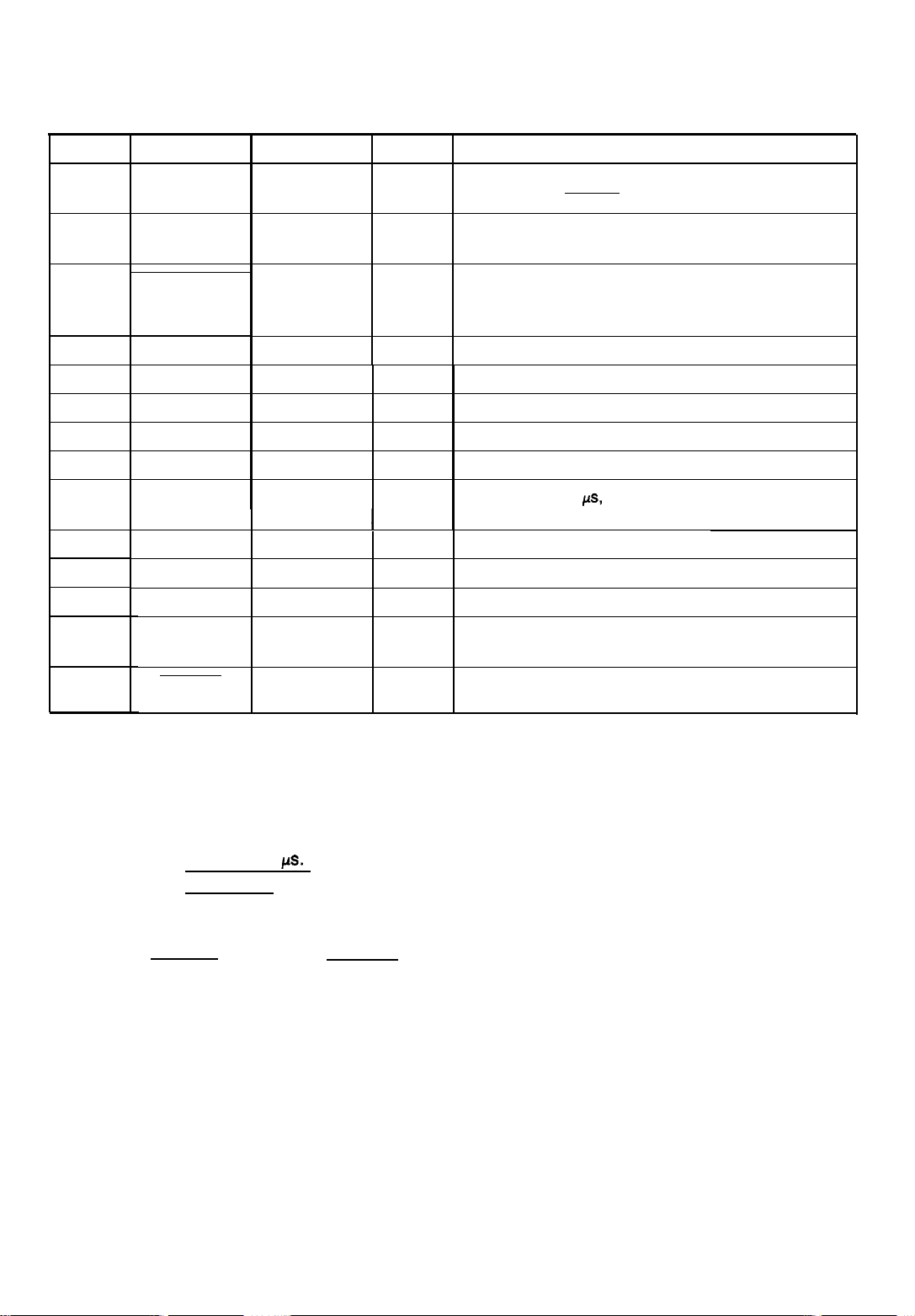
1.4 DIP SWITCHES AND JUMPER SETTING
This section describes the DIP switch selections and jumper setting for the LQ-510 printer.
1.4.1 DIP SWITCH SETTINGS
The two DIP switches for the printer are located on the control panel, and function as shown in Tables 1-11
through 1-15. (Note that the status of the DIP switches is read only at power up or upon receipt of the INIT
signal.)
1-16 LQ-510
Page 26
GENERAL DESCRIPTION
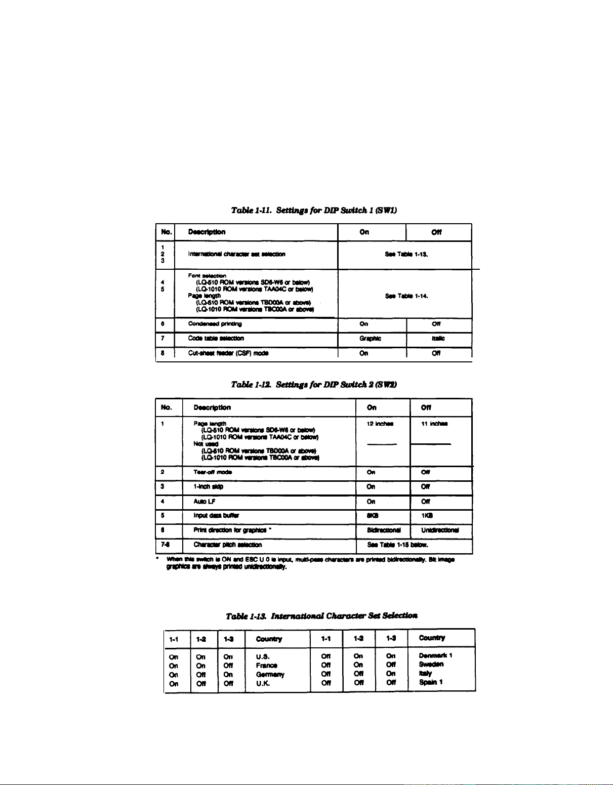
Table 1-14. Font Select&n
(ROM Version SD6-W6 or Below
or TAA04C or Below)
Table 1-15. Character Pitch Selection
2-7
Tab& 1-14. Page Length Selection
(ROM Version TBD00A or Above
or TBC00A or Above
Character Pitch
2-6 (ln characters per inch)
1.4.2 JUMPER SETTING
Jumper 10, which is user-selectable, is located inside the option board cover. If the jumper is connected,
the SLCT-IN signal is fixed to LOW, and DC1 /DC3 printer select control is ignored.
1.5 SELECTYPE FUNCTION
SelecType
fonts listed on the control panel for either condensed or normal printing.
optional slot-mounted multi-font (ROM cartridge), these fonts also can be selected from the control
panel. SelecType functions only when the printer is not printing, at which time the font can be
selected
switch (again,
printer’s control panel.
enables easy selection of fonts and
by pressing the FONT switch.
The printing
only when the printer is not printing).
printing modes, and can be used to select any of the
If the printer uses an
mode is selected by pressing the CONDENSED
The selected font and mode are indicated on the
LQ-510
1-17
Page 27

GENERAL DESCRIPTION
REV.-A
1.6 SHEET LOADING AND SHEET EJECTION
The release lever enables disengaging of the push tractor unit drive mechanism. The printer therefore provides some improved paper-handling functions through combination of the release lever and LOAD/EJECT
control panel switch.
Cut-Sheet Loading and Ejection
To load a sheet of paper, position the paper-release lever back, place the sheet along the paper guide, and
press the LOAD/EJECT switch. This loads the paper to the top-of-form position. Pressing the LOAD/EJECT
switch after the paper has been loaded will cause the paper to be ejected.
Continuous-Paper Loading and Ejection (Back-Out)
To load fanfold paper, move the paper-release lever forward, and insert the paper into the push tractor. Pressing
the LOAD/EJECT switch will then cause paper to be automatically loaded to the top-of-form position. Pressing the LOAD/EJECT switch after the fanfold paper has been loaded causes the printer to eject the paper
backward from the push tractor. To back out several pages, press the LOAD/EJECT switch several times
(reverse feed is performed on a page-by-page basis).
The MULTI-PART LED will flash only when the paper is loaded and the ON LINE switch pressed. This in-
dicates that the printer has entered “top-of-form adjust” mode, and that the user may adjust the top-of-form
position, as well as the loading positions for subsequent forms. Adjustment is made using the FORM FEED
button, which will increment the paper forward, and the LINE FEED switch, which will increment the paper
in reverse. (The minimum feed amount is 1/,80 inch.) When the cut-sheet feeder is used, the adjusted position
for the top of form will be lost after the printer is reinitialized, and the top of form will be reset to the default
value. When continuous paper is used, however, printer memory maintains the adjusted top-of-form position
even after printer initialization.
1.7 TEAR-OFF FUNCTION
If the tear-off function is enabled by making the appropriate DIP switch setting, it operates when the release
lever is set to the tractor position. In this case, if the input data buffer is empty and the printer is on line,
the paper is automatically fed to the tear-off position, and the MULTI-PART LED flashes to indicate that the
FORM FEED and LINE FEED switches are now available to perform micro-adjustment. The user may then
adjust the paper to the desired tear-off position. This position becomes the new tear-off position default, and
will remain valid even if the printer is reset and reinitialized, and regardless of whether the main power has
been interrupted. When new data is input to the printer, the paper is automatically returned to its original
position, and printing then starts. Paper that was advanced to the tear-off position will also be returned to
its original position if the ON LINE switch is pressed (switching the printer from on line to off line).
1-18
LQ-510
Page 28
REV.-A
GENERAL DESCRIPTION
1.8 OPERATING INSTRUCTIONS
This section describes the self-test and hexadecimal dump functions, error states, printer initialization, and
buzzer operation.
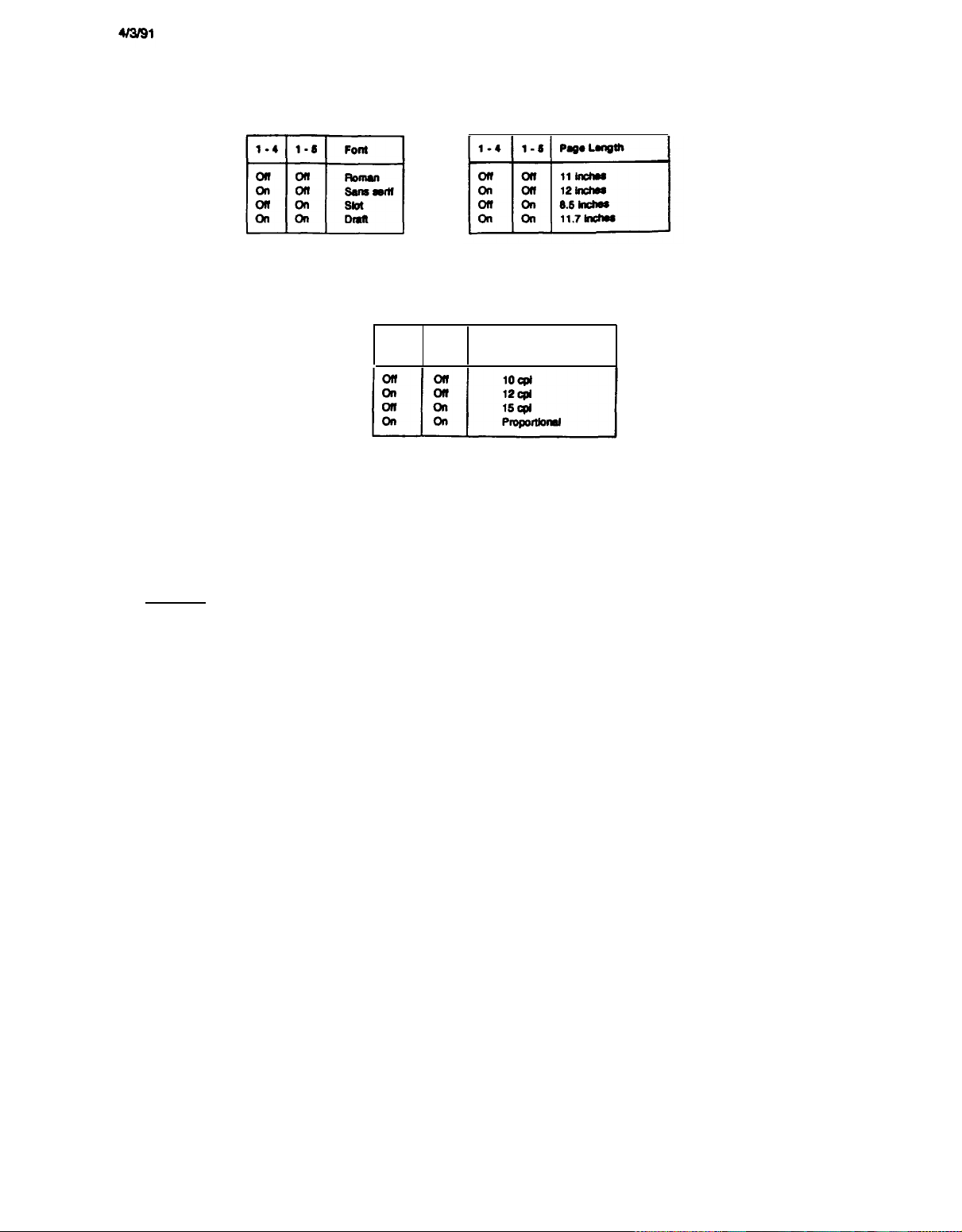
1.8.1 SELF-TEST
To begin self-test printing in draft mode, turn the printer on while depressing the LINE-FEED button. To begin
printing in letter-quality (LQ) mode, turn the printer on while depressing FORM FEED.
Self-test printing can be stopped and restarted by pressing ON LINE (this will not affect the ON-LINE in-
dicator). To conclude the self-test, press the ON-LINE switch to stop the printing; then turn off the printer.
The first printed line of the self-test indicates the firmware revision number. Following this line, the current
DIP switch settings are printed.
xxxxx
Country
USA
France
Germany
U.K.
Denmark
Sweden
Italy
Spain
Font
Roman
Sans serif
slot
Draft
Invalid
Valid
CG table
Italic
Graphic
CSF mode
Invalid
Valid
SW1-1 1-2 1-3
on on on
on on off
on off on
on off off
off on on
off on off
off off on
off off off
SW1-4 1-5
off off
on off
off on
on on
SW1-6
off
.3,:7
off
on
SW1-8
off
on
Page length
11"
12”
Tear off mode
Invalid
V&lid
I” skip
Invalid
Valid
Auto LF
Invalid
Valid
Receive buffer
1kbytes
8kbytes
Graphics print
uni-d
Bi-d
Pitch
10
pitch
12 Pitch
15 pitch
Proportional
off
on
Sw2-4
off
slz
off
2A
off
LQ-510
__.._ _-.
()a+.-
l*+.-./01234557S9::~=>?gAECDEFOHIJKLMNOWRSTUVNXYZ~\l-
Roman 10
01234567B9::~=~?6ABCDEPQHIJKLHNO~RSTWUXYZ~\]-~’~bcd.f6hijtl~no~r~tUVUX~6f:l1234667B9::<=>?~ABCDEFGHIJKLMNOWPSTVVYXYZl\1-
._
./0123456769:;~=~?OABCDEF(WIJKLNNOWRSTUVWXYZ(\]~~‘abcd~fghijklmnoPqr~tuvw
‘~bcd*fahljklmMKlratuvwx
‘abcd.fchl.ikl~nouar~tu~x~c(
Figure 1-8. Self-Test Printout
: I” !
1-19
Page 29

GENERAL DESCRIPTION
REV.-A
1.8.2 HEXADECIMAL DUMP FUNCTION
HEX dump mode is activated if the printer is switched on while both the LINE-FEED and FORM-FEED buttons are depressed. When this mode is in effect, the hexadecimal representation of the input data is printed
beside the corresponding printable ASCII characters. Periods (.) are printed beside control code input data.
This function is useful for checking the data the printer is receiving from the host.
Data Dump Mode
1B 40 0D 1B 55 00 1B 33 1E 00 0D 0A 0D 0A 0D 0A
12 1B 70 00 1B 78 01 1B 57 00 1B 4D 20 20 20 20
43 48 41 50 54 45 52 20 31 0D 0A 20 20 20 20 47
45 4E 45 52 41 4C 20 44
4F 4E 0D 0A 0D 0A 20 20 20 20 31 2E 31 20 46 45
41 54 55 52 45 53 0D 0A
53 50 45 43 49 46 49 43 41 54 49 4F 4E 53 0D 0A
20 20 20 20 20 20 20 20 31 2E 32 2E 31 20 46 61
72 64 77 61 72 65 20 53 70 65 63 69 66 69 63 61
74 69 6F 6E 73 0D 0A 20 20 20 20 20 20 20 20 31
2E 32 2E 32 20 46 69 72 6D 77 61 72 65 20 53 70
65 63 69 66 69 63 61 74 69 6F 6E 73 20 28 45 53
43 2F 50 29 0D 0A 20 20 20 20 31 2E 33 20 49 4E
54 45 52 46 41 43 45 20 4F 56 45 52 56 49 45 57
0D 0A 20 20 20 20 31 2E 34 20 44 49 50 20 53 57
49 54 43 40 45 53 20 41 4E 44 20 4A 55 4D 50 45
52 20 53 45 54 54 49 4E 47 0D 0A 20 20 20 20 20
20 20 20 31 2E 34 2E 31 20 44 49 50 20 53 77 69
74 63 68 20 53 65 74 74 69 6E 67 73 0D 0A 20 20
20 20 20 20 20 20 31 2E 34 2E 32 20 4A 75 6D 70
65 72 20 53 65 74 74 69 6E 67 0D 0A 20 20 20 20
31 2E 35 20 53 45 4C 45 43 54 59 50 45 20 46 55
4E 43 54 49 4F 4E 0D 0A 20 20 20 20 31 2E 36 20
53 48 45 45 54 20 4C 4F 41 44 49 4E 47 20 41 4E
44 20 53 48 45 45 54 20 45 4A 45 43 54 49 4F 4E
0D 0A 20 20 20 20 31 2E 37 20 54 45 41 52 2D 4F
46 46 20 46 55 4E 43 54 49 4F 4E 0D 0A 20 20 20
20 31 2E 38 20 4F 50 45 52 41 54 49 4E 47 20 49
4E 53 54 52 55 43 54 49 4F 4E 53 0D 0A 20 20 20
20 20 20 20 20 31 2E 38 2E 31 20 53 65 6C 66 2D
54 65 73 74 0D 0A 20 20 20 20 20 20 20 20 31 2E
30 2E 32 20 48 65 78 61 64 65 63 69 6D 61 6C 20
44 75 6D 70 20 46 75 6E 63 74 69 6F 6E 0D 0A 20
20 20 20 20 20 20 20 31 2E 38 2E 33 20 42 69 74
2D 49 6D 61 67 65 20 50 72 69 6E 74 69 6E 67 0D
0A 20 20 20 20 20 20 20 20 31 2E 38 2E 34 20 4.5
72 72 6F 72 20 43 6F 6E 64 69 74 69 6F 6E 73 0D
0A 20 20 20 20 20 20 20 20 31 2E 38 2E 35 20 42
75 7A 7A 65 72 20 4F 70 65 72 61 74 69 6F 6E 0D
0A 20 20 20 20 20 20 20 20 31 2E 38 2E 36 20 50
72 69 6E 74 65 72 20 49 6E 69 74 69 61 6C 69 7A
61 74 69 6F 6E 0D 0A 20 20 20 20 20 20 20 20 31
2E 38 2E 37 20 44 65 66 61 75 6C 74 20 56 61 6C
75 65 73 0D 0A 20 20 20 20 20 20 20 20 31 2E 38
2E 38 20 41 64 6A 75 73 74 20 4C 65 76 65 72 20
4F 70 65 72 61 74 69 6F 6E 0D 0A 20 20 20 20 20
20 20 20 31 2E 38 2E 39 20 50 72 69 6E 74 65 72
20 50 72 6F 74 65 63 74 69 6F 6E 20 66 6F 72 20
48 65 61 76 79 2D 44 75 74 79 20 50 72 69 6E 74
69 6E 67 0D 0A 20 20 20 20 31 2E 39 20 4D 41 49
4E 20 43 4F 4D 50 4F 4E 45 4E 54 53 0D 0A 20 20
20 20 20 20 20 20 31 2E 39 2E 31 20 53 41 4D 41
20 42 6F 61 72 64 0D 0A 20 20 20 20 20 20 20 20
31 2E 39 2E 32 20 53 41 4E 50 4E 4C 20 42 6F 61
72 64 0D 0A 20 20 20 20 20 20 20 20 31 2E 39 2E
33 20 53 41 4E 50 53 28 45 29 20 42 6F 61 72 64
0D 0A 20 20 20 20 20 20 20 20 31 2E 39 2E 34 20
50 72 69 6E 74 65 72 20 4D 65 63 68 61 6E 69 73
6D 20 28 4D 2D 35 37 31 30 29 0D 0A 20 20 20 20
20 20 20 20 31 2E 39 2E 35 20 48 6F 75 73 69 6E
67 0D 0A 0D 0A 20 20 20 20 31 2E 31 20 46 45 41
54 55 52 45 53 0D 0A 0D 0A 20 20 20 20 54 68 65
20 4C 51 2D 35 31 30 2F 35 35 30 20 69 73 20 61
45 53 43 52 49 50 54 49
20 20 20 20 31 2E 32 20
.@..U..3........
X..W..M
. .p..
CHAPTER 1..
ENERAL DESCRIPTI
ON.... 1.1 FE
ATURES. 1.2
SPECIFICATIONS..
rdware Specifica
tions..
.2.2 Firmware Sp
1.2.1 Ha
ecifications (ES
C/P). .
TERFACE OVERVIEW
ITCHES AND JUMPE
R SETTING..
1.4.1 DIP Swi
tch Settings..
er Setting..
1.5 SELECTYPE FU
NCTION.. 1.6
SHEET LOADING AN
D SHEET EJECTION
_ .
FF FUNCTION..
1.8 OPERATING I
NSTRUCTIONS..
1.3 IN
1.4 DIP SW
1.4.2 Jump
1.7 TEAR-O
1.8.1 Self-
Test. . 1.
8.2 Hexadecimal
Dump Function..
1.8.3 Bit
-Image Printing.
rror Conditions.
uzzer Operation.
rinter Initializ
1.8.4 E
1.8.5 B
1.8.6 P
ation..
.8.7 Default Val
ues.. 1.8
.8 Adjust Lever
Operation..
1.8.9 Printer
Protection for
Heavy-Duty Print
ing. _ 1.9 MAI
N COMPONENTS..
1.9.2 SANPNL Boa
rd.. 1.9.
3 SANPS(E) Board
. .
Printer Mechanis
m (M-5710)..
g.. . . 1.1 FEA
TURES.... The
1.9.1 SAMA
Board. _
1.9.4
1.9.5 Housin
LQ-510/550 is a
G
1
1
1-20
Figure 1-9. Hexadecimal Dump Function
LQ-510
Page 30
REV.-A
GENERAL DESCRIPTION
1.8.3 BIT-IMAGE PRINTING
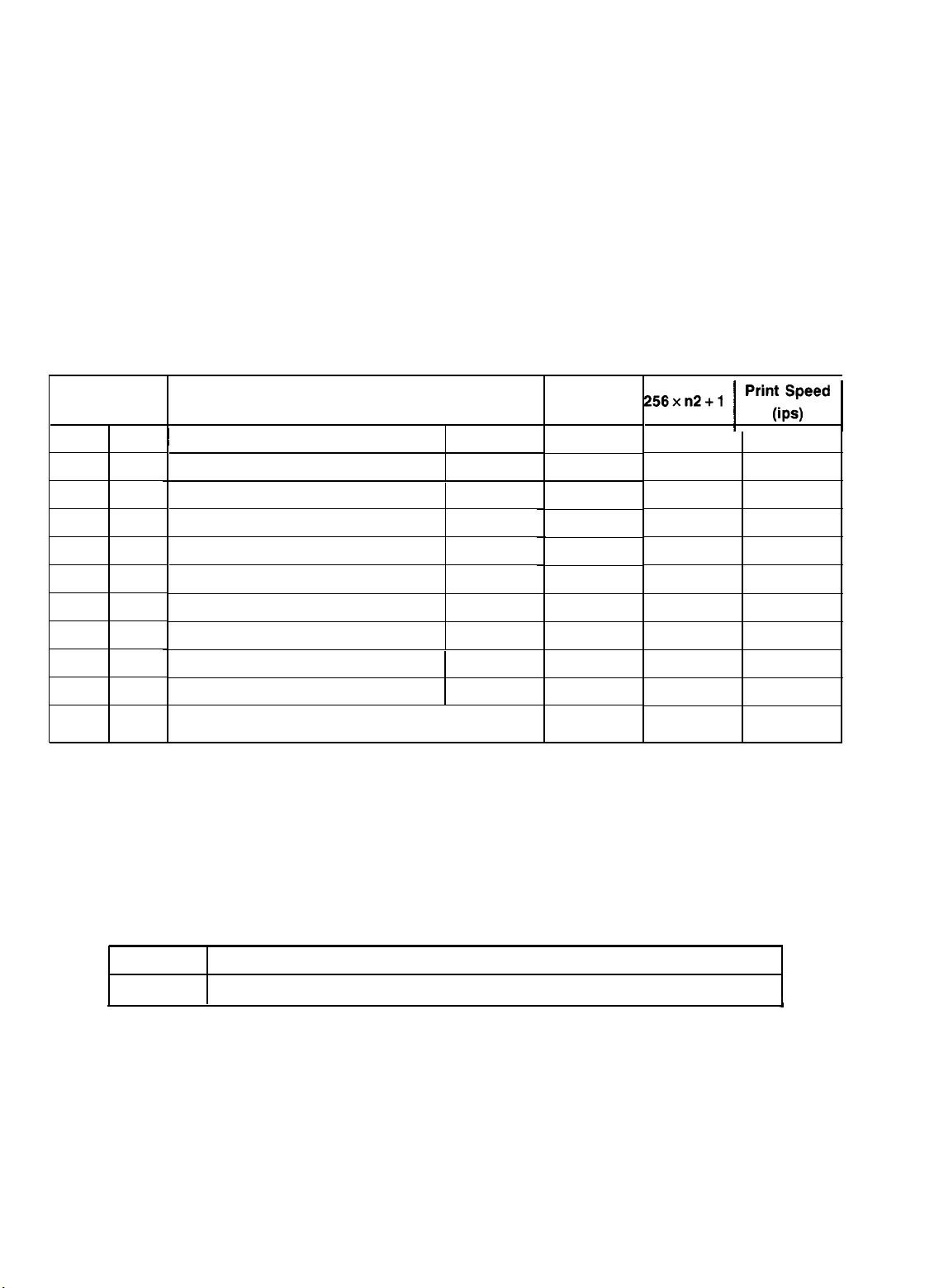
This printer offers the following four standard print densities (“dpi” indicates “dots per inch”):
120 dpi (including half dots): Triple speed
180 dpi (including half dots): Double speed
240 dpi (including half dots): 1.5 speed
360 dpi (including half dots): Normal speed
The firmware implements the print densities as shown in Table 1-16.
Table 1-16. Print Density
Pins m
8 0
8
8 2
8
8
8 6
24
24
24
24 39
24
NOTES:
Bit Image Printing Mode
~
Single-density
1
Dual density
Double speed, dual density
Quadruple density
3
4
CRT graphics
CRT graphics II
32
33
Single density
Dual density
CRT graphics II
38
Triple density
40
Hex. density
1. Dot density is in dots per inch; print speed is in inches per second.
Dot Density
(dpi)
60
120
120
240
80
I
90
60
120
90
180
360
I
2. The format of the graphics command is ESC* m n1 n2 [DATA]. Column 2 of the table shows
the significance of the various options for m.
The firmware handles the print densities as shown in Table 1-17.
Dot
Printing
yes
yes
no
no
yes
yes
yes
yes
yes
yes
no
256xn2+1 ! Prinii:eed 1
660
1320
1320
2640 7.5
880
990
660
1320 7.5
990
1980
3960
15
7.5
15
7.5
10
15
10
5
5
LQ-510
Dot Density
80 dpi
Table 1-17. Bit-Image Printing
Printing Method
Prints at 240 dpi by expanding the bit image by three: 80 x 3 = 240
I
1-21
Page 31

GENERAL DESCRIPTION
REV.-A
1.8.4 ERROR CONDITIONS
If any of the following error conditions are detected, the printer automatically enters off-line mode.
0 Home position is not detected at printer mechanism initialization.
0 Home position is detected during printing.
l
ON LINE is pressed when the printer is already on line. This will switch the printer to off line.
0 When a paper-out signal is detected and forms-override is finished.
l
If “paper out” is detected after the printer performs a paper-loading operation with the cut-sheet feeder
enabled.
The following interface signals are output to indicate the error and to halt data transmission:
BUSY signal becomes HIGH.
ERROR becomes LOW.
No ACKNLG pulse is sent.
1.8.5 BUZZER OPERATION
The buzzer operates as follows:
l
When the BEL code is sent to the printer, the buzzer sounds continuously for 0.5 seconds.
0
When the paper-out error is detected, the buzzer sounds 3 times, for 0.1 second each time. The interval
between sounds is 0.1 second.
0
When abnormal carriage movement is detected, the buzzer sounds 5 times, for 0.5 seconds each time.
The interval between sounds is 0.5 seconds.
0 When the panel setting is accepted, the buzzer sounds for 0.1 second.
1.8.6 PRINTER INITIALIZATION
There are two types of initialization: hardware initialization and software initialization.
Hardware Initialization
Hardware initialization occurs when the printer power switch is turned on (provided that the AC power cord
is plugged in), or when the INIT signal is received over the parallel interface line.
Upon hardware initialization, the printer does the following:
(a) Initializes the printer mechanism.
(b) Clears the input data buffer.
(c) Clears the downloaded character set.
(d) Clears the print buffer.
(e) Returns the printer settings to their default values.
Software Initialization
Software initialization occurs when the printer receives the software initialize code. For a software initialization, the printer does not perform the functions listed under (a), (b), and (c) above. Instead, the settings changed
by the last SelecType operation are reset.
1-22
LQ-510
Page 32

REV.-A
GENERAL DESCRIPTION
1.8.7 DEFAULT VALUES
When the printer is initialized, the following default values and functions are set:
Page Position
Left and Right Margin
Line Spacing
Vertical Tabs
Horizontal Tabs
VFH Channel
The current paper position becomes the top-of-form position
Released
1/6 inch
Cleared
Every 8 characters (relative)
Channel 0
Family Number of Type
Style
Download Characters
Font selected by DIP switch
Deselected (if software initialization)
Cleared (if hardware initialization)
Justification
Character Spacing
Bit-Image Mode Assignment
Printing Effects
Condensed Printing
Left justification
10 cpi
ESC K = ESC* 0, ESC L = ESC * 1
ESC Y =
ESC * 2, ESC Z = ESC * 3
All effects other than condensed printing are cleared
Setting selected by DIP switch
1.8.8 ADJUST LEVER OPERATION
The position of the adjust lever must be set to accord with the paper thickness. If the lever is set to position
four or above, the MULTI-PART indicator lights and the printing speed is increased. See Table 1-18 and
Figure 1-10.
Table 1-18. Lever Position
l
If the printing density is light, position the adjust lever one step lower.
2nd position
I
4th position
Figure 1-10. Lever Position
LQ-510/550
1-23
Page 33

GENERAL DESCRIPTION
1.8.9
PRINTER PROTECTION FOR HEAVY-DUTY PRINTING
REV.-A
The printer incorporates “printhead protection” to safeguard it from overheating and from the potential ill
effects of a voltage drop to the head driver. If the temperature of the head exceeds a specified value, printing
is automatically suspended. Printing automatically resumes when the temperature drops to another specified
value.
If heavy-duty printing causes the voltage to the head drive circuit to drop to a specified value, printing is
immediately suspended. If the voltage recovers, the line that was being printed is completed. This protection
occurs when half or more of the wires are activated simultaneously and continuously.
1-24
LQ-510
Page 34

REV.-A
GENERAL DESCRIPTION
1.9 MAIN COMPONENTS
To facilitate maintenance and repair, the main components of the LQ-510 printer are designed so that they
can be removed and replaced easily.
The main components are:
1) SAMA board:
The main control board. The CPU, which is contained on
this board, controls all the main functions.
2) SANPNL control panel:
3) SANPS board: (120 V Version)
The control panel.
The power supply circuit board.
SANPSE Board (220/240 V Version)
4) M-5710: The printer mechanism.
I
SANPS(E) Board
M
SAMA Board
LQ-510
M-5710 Printer Mechanism
Figure 1-11. LQ-510 Component Layout
1-25
Page 35

GENERAL DESCRIPTION
1.9.1 SAMA BOARD
REV.-A
The use of the
E05A02 Gate Array (1A)
pPD7810HG
CPU simplifies the circuitry design of the main control board.
1MCG M10A17 or M10A20
PSRAM (5A)
27256 PROM (6A)
Gate
Array
(71
pPD7810HG CPU (5B)
Figure 1-12. SAMA Main Control Board
1-26
LQ-510
Page 36

REV.-A
1.9.2 SANPNL CONTROL PANEL
The SANPNL control panel, which is the LQ-510’s control panel, contains the switches and the indicator
LEDs illustrated below.
GENERAL DESCRIPTION
LQ-510
Figure 1-13. SANPNL Control Panel
1-27
Page 37

GENERAL DESCRIPTION
REV.-A
1.9.3 SANPS(E) BOARD
The power supply circuit (SANPS/SANPSE board), which is housed at the upper left of the lower case, consists of a line filter, fuse, power switch, and switching regulator circuit. It converts the AC line voltage to
the + 24 V, + 12 V, - 12 V, and + 5 VDC voltages used by the printer.
(SANPS Board)
(SANPSE Board)
Figure 1-14. Power Supply Filter Board
1.9.4 PRINTER MECHANISM (M-5710)
The M-5710 printer mechanism was developed expressly for use with LQ-510 printer. Its components include a carriage motor, carriage mechanism, paper-feed motor, paper-feed mechanism, ribbon-feed
mechanism, printhead, and sensors.
1-28
Figure 1-15. Model 5710 Printer Mechanism
LQ-510
Page 38

REV.-A
1.9.5 HOUSING
GENERAL DESCRIPTION
The housing for the LQ-510 consists of upper and lower
cases.
The upper case houses the control panel.
The lower case contains the printer mechanism and the main control board. The printer cartridge can be
removed and replaced easily.
Figure 1-16. Housing
LQ-510
1-29
Page 39

REV.-A
PRINCIPLES OF OPERATION
CHAPTER 2
PRINCIPLES OF OPERATION
2.1
OVERVIEW
2.1.1
2.1.2 Outline of Printer Mechanism Operation
2.1.3 Circuit Overview
2.2 OPERATION OF THE POWER SUPPLY CIRCUIT
2.2.1
2.2.2 Filter Circuit........................................................................
2.2.3 Rectifier and Smoothing Circuit
2.2.4
2.2.5
2.2.6
2.2.7 Voltage Limiting Circuit .......................................................
2.2.8 ± 12 VDC Supply Circuit
2.3 PRINTER MECHANISM AND CONTROL CIRCUIT OPERATION
2.3.1
2.3.2 Reset Circuit
2.3.3 Address Decoder and Bank Register
2.3.4 Carriage Operation
2.3.5 Paper Feed .........................................................................
....................................................................................
Connectors Summary
2.1.2.1 Sensors
2.1.2.2
2.1.2.3 Printhead
2.1.3.1 Overview of Power Supply Circuit
2.1.3.2
Power Supply Circuit Block Diagram
Starting Circuit (Main Switching Circuit)
+ 24 VDC Voltage Control Circuit
+ 5 VDC Regulator Circuit
Vx Voltage Supply Circuit
2.3.4.1 Carriage Mechanism
2.3.4.2 Carriage Motor Specifications
2.3.4.3 Carriage Motor Drive Circuit Block Description..
2.3.4.4
2.3.4.5
2.3.4.6
2.3.5.1 Paper-Feed Mechanism Operation
2.3.5.2 Paper-Feed Motor Specifications
2.3.5.3
2.3.5.4
Motors
Control Circuit Block Diagram
.......................................................................
Gate Array E01A05 Operation in Carriage Motor
Drive Circuit
Carriage Motor Drive Circuit
Carriage Motor Software Control
Paper-Feed Motor Drive Circuit
Paper-Feed Motor Software Control
..........................................................
...............................
...............................................................
.................................................................
.............................................................
.................................................................
..........................
................................
...............................
....................................
............................................
................................
.........................................
....................................................
......................................................
............
....................................................
....................................
..............................................................
..............................................
................................
.........................................................
..................................
............................
..........................
............................
..............................
.......................
.....
2-1
2-1
2-3
2-4
2-9
2-9
2-10
2-10
2-11
2-13
2-13
2-14
2-15
2-15
2-19
2-21
2-25
2-26
2-27
2-27
2-28
2-33
2-35
2-35
2-36
2-36
2-37
2-38
2-47
2-51
2-51
2-52
2-53
2-54
LQ-510
2-i
Page 40

PRINCIPLES OF OPERATION
REV.-A
2.3.6 Printhead
2.3.6.1 Printhead Printing Operation
2.3.6.2 Printhead Specifications
2.3.6.3
2.3.6.4
2.3.6.5 Printhead Drive Circuit ..........................................
2.3.6.6 Printhead Software Control
2.3.7 A/D Converter Circuit
2.3.8 Host Interface
2.3.9 EEPROM Circuit ..................................................................
2.3.10 Ribbon-Feed Mechanism
............................................................................
.................................
........................................
Printhead Drive Circuit Block Diagram..
Gate Array E05A02 Operation in Printhead
Drive Circuit
.....................................................................
.........................................................
...................................
..........................................................
......................................................
LIST OF FIGURES
Figure 2-1.
Figure 2-2.
Figure 2-3.
Figure 2-4.
Figure 2-5.
Figure 2-6.
Figure 2-7.
Figure 2-8.
Figure 2-9.
Figure 2-10.
Figure 2-11.
Figure 2-12.
Figure 2-13.
Figure 2-14.
Figure 2-15.
Figure 2-16.
Figure 2-17.
Figure 2-18.
Figure 2-19.
Figure 2-20.
Figure 2-21.
Figure 2-22.
Cable Connections
Printer Mechanism Block Diagram
Paper-End Sensor Mechanism
Paper-End Sensor Circuit
Home-Position Sensor Mechanism
Home-Position Sensor Circuit
Thermal Sensor Mechanism (Printhead Temperature
Detection)
Thermal Sensor Circuit
Platen Gap Sensor Mechanism
Platen Gap Sensor Circuit
Friction/Tractor Sensor Mechanism
Friction/Tractor Sensor Circuit
Printhead
Overview of
Control Circuit Block Diagram
Power Supply Circuit Block Diagram
Filter Circuit (SANPS Board,
Filter Circuit (SANPSE Board, 220/240 V Version)
Rectifier and Smoothing Circuit
Starting Circuit (Main Switching Circuit)
Main Switching Circuit Waveforms
+24 VDC Voltage Control Circuit
.......................................................................
........................................................................
...........................................................
....................................
..........................................
.................................................
....................................
...........................................
....................................................
.........................................
................................................
..................................
.........................................
Power Supply Circuit Operation
..........................................
.................................
120 V Version).
........................................
............................
....................................
......................................
..................
.....................
.....................
.............
2-55
2-55
2-55
2-56
2-57
2-56
2-59
2-60
2-63
2-64
2-65
2-2
2-3
2-4
2-4
2-5
2-5
2-6
2-6
2-7
2-7
2-8
2-8
2-9
2-10
2-11
2-13
2-14
2-14
2-15
2-17
2-18
2-19
2-ii
LQ-510
Page 41

REV.-A
PRINCIPLES OF OPERATION
Figure 2-23.
Figure 2-24.
Figure 2-25.
Figure 2-26.
Figure 2-27.
Figure 2-28.
Figure 2-29.
Figure 2-30.
Figure 2-31.
Figure 2-32.
Figure 2-33.
Figure 2-34.
Figure 2-35.
Figure 2-36.
Figure 2-37.
Figure 2-38.
Figure 2-39.
Figure 2-40.
Figure 2-41.
Figure 2-42.
Figure 2-43.
Figure 2-44.
Figure 2-45.
Figure 2-46.
Figure 2-47.
Figure 2-48.
Figure 2-49.
Figure 2-50.
Figure 2-51.
Figure 2-52.
Figure 2-53.
Figure 2-54.
Figure 2-55.
Figure 2-56.
Figure 2-57.
Figure 2-58.
Figure 2-59.
Figure 2-60.
Figure 2-61.
Figure 2-62.
Switching Circuit (During PCI Operation)
Over-Current Protection (OCP)
+ 5 VDC Regulator Circuit
Oscillator Waveforms
.......................................................
Constant Voltage Control
EAI Output
......................................................................
Over-Current Protection (OCP)
lC494 Internal Circuit
PWM Output
....................................................................
Voltage Limiting Circuit
.......................................................
....................................................
± 12 VDC Supply Circuit
Vx Voltage Circuit
Reset Circuit
RESET Output
............................................................
...................................................................
.................................................................
..........................................
................................................
.................................................
..........................................
.................................................
...........................
RESET Pulse Oscillation Process (Module Mounted).
RESET Pulse Oscillation Process (Module Removed)
INIT Signal Input Circuit
Address Decoder
Bank Register
.............................................................
..................................................................
Carriage Mechanism
Carriage Drive Circuit Block Diagram
Gate Array Operation
Carriage Motor Drive Circuit
SLA7020M Circuit Diagram
Phase Data Input Timing (2-2 Phase)
Phase Signal Timing Chart (2-2 Phase)
Phase Data Input Circuit (1-2 Phase)
Phase Signal Timing Chart (1-2 Phase)
Phase Data Conversion Circuit
Reference Voltage Generation Circuit
Constant Current Control Circuit
Waveforms
......................................................................
Carriage Motor Control
Home-Position Seek
Printing Area and Printing Timing
Friction-Feed Operation
Push-Tractor-Feed Operation
Paper-Feed Motor Drive Circuit
Paper-Feed Motor Drive Timing Chart
Printhead Printing Operation
...................................................
........................................................
................................
.......................................................
.............................................
...............................................
................................
.............................
.................................
.............................
.........................................
...............................
.......................................
.....................................................
.........................................................
.....................................
...................................................
............................................
.........................................
...............................
............................................
.........
.........
2-20
2-20
2-21
2-22
2-22
2-22
2-23
2-24
2-24
2-25
2-26
2-27
2-28
2-29
2-30
2-31
2-32
2-33
2-34
2-35
2-36
2-37
2-38
2-39
2-40
2-40
2-41
2-41
2-42
2-43
2-44
2-45
2-48
2-49
2-50
2-51
2-52
2-53
2-54
2-55
LQ-510
2-iii
Page 42

PRINCIPLES OF OPERATION
REV.-A
Figure 2-63.
Figure 2-64.
Figure 2-65.
Figure 2-66.
Figure 2-67.
Figure 2-68.
Figure 2-69.
Figure 2-70.
Figure 2-71.
Table 2-1.
Table 2-2.
Table 2-3.
Table 2-4.
Table 2-5.
Table 2-8.
Table 2-7.
Table 2-8.
Table 2-9.
Table 2-10.
Printhead Drive Circuit Block Diagram
Printhead Drive Circuit
Printhead Drive Waveforms
Print Timing
Relationship Between Head Driving Voltage and Print
Driving Pulse Width
A/D Converter Circuit
Host Interface
EEPROM Circuit
Ribbon-Feed Mechanism
....................................................................
.................................................................
.....................................................
..............................................
.........................................................
......................................................
..............................................................
..................................................
..............................
LIST OF TABLES
Board Connector Summary
Power Supply Applications
Reference Voltages
Phase-Excitation Method
Drive Sequence (2-2 Excitation)
Drive Sequence (1-2 Excitation)
Excitation Sequence
E05A02 Gate Array Functions
Scan Lines and DIP Switches
Ribbon-Feed Gear Train
..........................................................
........................................................
..............................................
...............................................
..................................................
........................................
........................................
...........................................
...........................................
...................................................
2-66
2-57
2-58
2-59
2-59
2-61
2-63
2-64
2-65
2-1
2-10
2-43
2-47
2-47
2-47
2-54
2-57
2-62
2-66
2-iv
LQ-510
Page 43

REV.-A
PRINCIPLES OF OPERATION 2
2.1 OVERVIEW
This chapter describes the signals at the connectors linking the primary components of the LQ-510. These
components include the printer mechanism, power supply circuits, and control circuits. The chapter also
describes the operation of the printer’s circuitry and printer mechanism.
2.1.1 CONNECTOR SUMMARY
The interconnection of the primary components is illustrated in Figure 2-1. Table 2-1 summarizes the functions, sizes, and types of the connectors shown in the figure.
LQ-510
2-1
Page 44

PRINCIPLES OF OPERATION
REV.-A
SANPNL-W
Control Panel
Board
Model 5710 Printer Mechanism
PF
Friction/Tractor PG CR
Sensor Sensor
2-pin 2-pin 12-pin 15-pin 17-pin
Motor
SAMA Board
Head
PE Home
SANPS(E)
BOARD
NOTE:
Parallel I IF
I
I
CR = carriage.
PF
= paper feed.
Optional
Interface
Board
Serial I/F
I
Host Computer
Figure 2-1. Cable Connections
SW Board
I
AC IN
I
I
2-2
LQ-510
Page 45

REV.-A
2.1.2 OUTLINE OF PRINTER MECHANISM OPERATION
The Model 5710 printer mechanism is a serial, impact, dot-matrix mechanism that prints at 180 dots per
inch (dpi) in both horizontal and vertical directions. Figure 2-2 shows a block diagram of the printer mechanism.
PRINCIPLES OF OPERATION
TEMP
Printhead
Temperature
; -
. - - . . . .
Phase
stepper Motor
Carriage Drive
Phase
stepper Motor
-/step
PE
ADJUST RELEASE
PLATEN GAP
Release
Position
&
Lever
NOTE: CW = clockwise; CCW = counterclockwise,
HP = home position.
PE = paper end.
Figure 2-2. Printer Mechanism Block Diagram
LQ-510
2-3
Page 46

PRINCIPLES OF OPERATION
REV.-A
2.1.2.1 Sensors
The printer mechanism is equipped with the following sensors:
Paper-End (PE) Sensor
Home-Position (HP) Sensor
Thermal Sensor (for sensing printhead temperature)
Platen Gap (PG) Sensor
Friction/Tractor Sensor
Paper-End Sensor (PE Sensor)
Figures 2-3 and 2-4 show the paper-end sensor. This sensor switch is ON when no paper is in place (e.g.,
when the paper supply has run out).
Paper out + ON -, LOW
Paper present + OFF -, HIGH
Paper out
Figure 2-3. Paper-End Sensor Mechanism
2-4
Figure 2-4. Paper-End Sensor Circuit
LQ-510
Page 47

REV.-A
PRINCIPLES OF OPERATION
Home-Position Sensor (HP Sensor)
Figures 2-5 and 2-6 show the home-position sensor. The sensor switch is ON when the carriage is at the
home position.
+
Home position
Other positions
ON + LOW
+
OFF + HIGH
The reference position for the carriage drive is determined by this sensor.
shaft
Home-Position Sensor
Figure 2-5. Home-Position Sensor Mechanism
Figure 2-6. Home-Position Sensor Circuit
LQ-510
2-5
Page 48

PRINCIPLES OF OPERATION
REV.-A
Thermal Sensor (Printhead Temperature Detection)
The thermal sensor in the printhead monitors the printhead temperature. If the head temperature exceeds
a specified upper limit, printing is automatically suspended. Printing resumes when the temperature drops
to a specified lower value. Figure 2-8 illustrates the printer’s thermal-sensor circuit.
Printhead
‘-Thermal
Sensor
Figure 2-7. Thermal Sensor Mechanism (Printhead Temperature Detection)
V
AREF
R50
3.3K
b
TEMP
10K
I
0.1
T
AVss
Thermal
Sensor
in Head
CN8-16
n
”
CN8-17
r\
”
Figure 2-8. Thermal Sensor Circuit
2-6
LQ-510
Page 49

REV.-A
PRINCIPLES OF OPERATION
Platen Gap (PG) Sensor
The PG sensor is ON whenever the adjust lever position is set to the fourth position or above. If the sensor
is ON, printing will be in multiple copy mode, and the print speed will be relatively slow.
Adjust Lever
Adjust Lever
Platen Gap
Position1to3-,
4
Position
to7-,
2 nd position
OFF -, HIGH
ON - LOW
6 th position
Platen Gap (PG) Sensor
Figure 2-9. Platen Gap Sensor Mechanism
Figure 2-10. Platen Gap Sensor Circuit
LQ-510
2-7
Page 50

PRINCIPLES OF OPERATION
REV.-A
Friction/Tractor Sensor
The friction/tractor sensor detects the position of the release lever to determine whether tractor feed or fric-
tion feed is in effect.
Release Lever Position: Front - Friction Feed + OFF - HIGH level
Release Lever Position: Rear + Tractor Feed -, ON + LOW level
Front
Friction/Tractor Sensor
Rear
Release Lever
Figure 2-11. Friction/Tractor Sensor Mechanism
2-8
Figure 2-12. Friction/Tractor Sensor Circuit
LQ-510
Page 51

REV.-A
2.1.2.2 Motors
This printer has the following motors:
Carriage motor (stepper motor)
Paper-feed motor (stepper motor)
Carriage Motor
The carriage motor is used to move the carriage right and left along the platen. This unit employs a four-
phase, 48-step motor using either 1-2 or 2-2 phase excitation and is controlled by an open-loop system.
Paper-Feed Motor
Paper is fed using a four-phase, 48-step motor operating with either 1-2 or 2-2 phase excitation, which ad-
vances the paper either 1/180 inch or 1/360 inch for each phase switch. The CPU controls the motor through
an open loop.
2.1.2.3 Printhead
PRINCIPLES OF OPERATION
Figure 2-13 shows the dot-wire operation. When the head-driving coil is energized, the dot wire is pushed
out. The dot wire strikes the ribbon, causing the ribbon to impact the paper, thereby printing a dot.
Platen
Dot wire
.-y
Head
Iron
-
Driving
coil
\ Paper
Core
Figure 2-13. Printhead
LQ-510
2-9
Page 52

PRINCIPLES OF OPERATION
REV.-A
2.1.3 Circuit Overview
This section describes the circuitry.
2.1.3.1 Overview of the Power Supply Circuit
The
power circuit for this system is an SANPS(E) board. The circuit converts the AC power source to the
+ 24, + 5, and ± 12 VDC that the unit requires.
To SAMA Board
+
+24VDC
AC IN
(12OVAC or
220/240VAC)
Figure 2-14. Overview of Power Supply Circuit Operation
Voltage
+5v
+24 V
±12 v
VX
m
SANPS (120V Ver)
SANPSE (220/24OV Ver)
Table 2-2. Power Supply Applications
Application
Logic circuit
Paper-feed motor holding voltage, etc.
Carriage motor drive voltage
Paper-feed motor drive voltage
Printhead drive voltage
Optional I/F voltage
Reset circuit
Printhead data signal pull-up voltage
Paper-feed motor phase data signal pull-up voltage
*
+5VDC
)
+12VDC
b-12VDC
NOTE:
2-10
The voltage Vx is generated on the SAMA board using the + 5 V power supply.
LQ-510
Page 53

REV.-A
2.1.3.2 Control Circuit Block Diagram
Figure 2-15 shows a block diagram of the control circuitry.
ADDRESS MAPPING
0000H 4000H
I
8000H
PRINCIPLES OF OPERATION
A000H
I
I
F000H
NOTE: CG
GA
LQ-510
= character generator.
= gate array.
Figure 2-15. Control Circuit Block Diagram
2-11
Page 54

PRINCIPLES OF OPERATION
The control circuit consists mainly of the following ICs:
0 µPD7810HG CPU (5B)
The µPD7810HG executes the program in the PROM (6A) and controls all the printer operations. Upon receiv-
ing the RESET signal, the CPU begins executing the program from address 0000 hex.
. PROM (6A)
The PROM includes the control program (firmware).
0 HM65256 PSRAM (5A)
The HM65256 PSRAM is external memory for the CPU. It is used as an input data buffer and line buffer
for expanding data, and as working area for the program.
0 E01A05 Gate Array (7A)
The E01A05 functions are as follows:
1. Parallel I/F
2. Address decoder
3. Bank register
4. Data address multiplexer
5. Reset
6. CR motor control
REV.-A
0
E05A02 Gate Array (1 A)
The E05A02 was developed for 24pin, dot-matrix printers and is used to simplify the interface between the
CPU and the printhead.
0
EEPROM (7B)
The EEPROM has a 128-bit memory, which is used to store the paper position.
0 M10A17 or M10A20 Mask ROM (1M CG, 4A)
The M10A17 or M10A20 mask ROM incorporates the character generators. The ROM includes character
design.
Other control circuits are as follows:
0 Paper-Feed Motor Drive Circuit
This circuit drives the paper-feed motor, which is a four-phase, stepper motor. The CPU controls the motor’s
rotation (position and speed).
0 Carriage Motor Drive Circuit
The carriage motor drive circuit drives the carriage motor, which is a four-phase stepper motor. The rotation
of the motor (position and speed) is controlled by outputting the phase switching signal by the E01A05 gate
array.
2-12
LQ-510
Page 55

REV.-A
PRINCIPLES OF OPERATION
2.2 OPERATION OF THE POWER SUPPLY CIRCUIT
The power circuit used in the printer is either a 120 V SANPS board for the U.S., Taiwan, and the Middle
East or a 220/240 V SANPSE board (for Europe, Asia, etc.). The basic operation of both boards is the same,
however, and they are treated as one in this manual.
2.2.1 POWER SUPPLY CIRCUIT BLOCK DIAGRAM
Figure 2-18 shows the power supply circuit block diagram. The SANPS(E) board uses a forward-convertor
type switching regulator circuit, and outputs + 5, + 24, and + 12 VDC.
The incoming AC power passes first through a noise filter, then through a full-wave rectifying circuit. The
power then passes into the main switching circuit, which outputs + 24 V and ± 12 VDC. Stabilization is pro-
vided by an over-voltage limiting circuit located on the 24 V line, which feeds back to the main switching
circuit. The 24 V line is also used to generate the 5 V output.
LQ-510
OVER VOLTAGE PROTECTION
Figure 2-16. Power Supply Circuit Block Diagram
2-13
Page 56

PRINCIPLES OF OPERATION
REV.-A
2.2.2 FILTER CIRCUIT
The input filter is a conventional LC filter circuit that functions both to dampen incoming noise and to prevent
externally generated noise from running though the AC line. All the circuit’s coils and condensers are designed
to withstand fluctuations in the incoming AC power.
Figure 2-17. Filter Circuit (SANPS Board, 120 V Version)
Figure 2-16. Filter Circuit (SANPSE Board, 220/240 V Version)
2-14
LQ-510
Page 57

REV.-A
PRINCIPLES OF OPERATION
2.2.3 RECTIFIER AND SMOOTHING CIRCUIT
The AC IN voltage from the filter circuit is full-wave rectified by diode bridge DB1, and converted to approx-
imately 2 x AC IN voltage by smoothing capacitor C7. The + 24 VDC, + 5 VDC, and ± 12 VDC voltages
are converted from this DC voltage.
DB1
NOTE:
The item in parentheses pertains to the 220/240 V version
Figure 2-19. Rectifier and Smoothing Circuit
2.2.4 STARTING CIRCUIT (MAIN SWITCHING CIRCUIT)
Figure 2-20 shows the starting circuit. The operation sequence is as follows.
(1) When the main power source is connected, the AC input passes through the input filter and is then rec-
tified and smoothed. The resulting DC voltage VIN is input into the circuit.
(2) VIN is applied to starting resistance R7 and passes through point A. Base current lB flows through tran-
sistor Q1, causing the transistor to conduct.
(3) At the same time,
at 8-2, so that the positive feedback current of switching circuit
VIN
is applied to coil 4-3 of pulse transformer T1, causing a voltage of (7/60T)
IB
flows in the direction of B. This causes
(VIN)
a sharp rise, and Q1 quickly switches on.
(4) Current
induced through coils 7-8 and 8-11, and a voltage of (19/60T)
IL
through coil 4-3 increases linearly over time. During this time, a voltage of (10/60T)
VIN
through coil 9-10. For all these coils,
VIN
is
then, current attempts to flow in the direction of D; however, this direction opposes the direction of diodes
D22, D23, and D20, so that no current flows through the secondary side of the circuit.
LQ-510
2-15
Page 58

PRINCIPLES OF OPERATION
REV.-A
(5) Current
IL
in the primary winding increases, but because the potential at point 6 of coil 6-2 is fixed, Q1
base current IB cannot surpass a specified level. As a result of this, the value of current Ic (= IL) flow-
ing from coil 4-3 to the Q1 collector cannot surpass a maximum of hfe
(1~).
Therefore, the 4-3 current
value stops changing, and the coil voltage drops. At the same time, a reverse voltage is applied to coil
6-2, IB drops, and current flows through D3 opposite to direction B. At this time, the potential at point
A is higher than that at point E, and C10 absorbs the current flowing in the A-E direction. Q1 is quickly
shut off by the resulting sharp drop.
(6) The above process causes the energy previously induced in the secondary side (in step (4), above) to
be released from coils 7-8, 8-11, and 9-10 in the direction opposite to D, and current flows in the easy-
flow direction of the diodes. Therefore, the secondary side outputs a voltage.
(7)
The release of energy declines linearly over time. When energy release is completed, all T1 coil voltages
momentarily reach zero. R3, however, again induces switching current lB in the direction of B, and Q1
conducts. Because the potential at point E then surpasses that at point A, the energy in C10 is released,
so that IB is maintained.
(8)
The sequence returns to the stage described in (3) above. This repetition enables the circuit to maintain
oscillation. R7 is involved, however, only at the start time.
The above sequence is generally known as a self-excitation type ringing choke converter (RCC) configuration.
Note that, at the instant when Q1 goes off (in step (5), above), the potential at point F jumps violently upward,
but because of the action of D2, the energy is fed into R5 and consumed.
Below are shown the waveforms for each part of the circuit.
As Figure 2-21 makes clear, the output voltage is controlled by the time period that Q1 is off. In other words,
the circuit is controlled by controlling the period during which Q1 is off.
2-16
LQ-510
Page 59

REV.-A
PRINCIPLES OF OPERATION
0
7
0
B2
n
NOTE:
items in parentheses refer to the 220/240 V version.
Figure 2-20. Starting Circuit (Main Switching Circuit)
LQ-510
2-17
Page 60

PRINCIPLES OF OPERATION
REV.-A
NOTE:
2-18
Output
Current
Items in parentheses refer to the 220/240 V version.
Figure 2-21. Main Switching Circuit Waveforms
LQ-510
Page 61

REV.-A
2.2.5 +24 VDC VOLTAGE CONTROL CIRCUIT
Figure 2-22 shows the + 24 VDC voltage control circuit. To maintain the correct voltage on the + 24 V line,
the main switching transistor goes off if the voltage exceeds 24 V. If excess voltage occurs, reverse current
flows through Zener diode ZD20, PC1 is activated, and the condition of the switching circuit is as shown
in Figure 2-23.
r
/
D4
PRINCIPLES OF OPERATION
C10
0.01
R8
ON
1
-
+24V DC
-I-
GND
4
NOTE:
LQ-510
Items in parentheses refer to the 220/240 V version.
Figure 2-22. +24 VDC Voltage Control Circuit
2-19
Page 62

PRINCIPLES OF OPERATION
REV.-A
When PC1 is activated, the voltage at shunt regulator gap G reaches at least 2.5 V, K-A becomes a conductor, Q3 goes on, Q2 goes on, and shunt transistor Q1 goes off.
Even if PC1 is not activated, K-A will conduct if current I in the transformer’s primary winding surpasses
a certain value, creating a potential difference of at least 2.5 V across resistance R4. Resistance R4, in other
words, serves as an excess current detector.
NOTE:
NOTE:
Items in parentheses refer to the 220/240 V version.
Figure 2-23. Switching Circuit (During PC1 Operation)
Items in parentheses refer to the 220/240 V version.
2-20
Figure 2-24. Over-Current Protection (OCP)
LQ-510
Page 63

REV.-A
PRINCIPLES OF OPERATION
2.2.6 +5 VDC REGULATOR CIRCUIT
Figure 2-25 shows the + 5 VDC Regulator Circuit. The + 5 VDC is generated from the + 24 VDC by a choppertype switching regulator circuit utilizing a TL494. Through pin 13 of the output control terminal, the TL494
can cause the IC to operate in either push-pull or parallel mode. In the illustration, pin 13 is LOW, and parallel
action is in effect. In other words, the operation of the IC’s two output transistors will be exactly alike.
The IC incorporates an internal oscillating circuit. The oscillating frequency is determined by the external
inputs to pins 5 and 6. In this circuit, the frequency, set by R29 and C25, is about 27K Hz.
LQ-510
Figure 2-25. +5 VDC Regulator Circuit
2-21
Page 64

PRINCIPLES OF OPERATION
REV.-A
EA1 and EA2 in the IC are error amplifiers. EA2 is used to detect the output voltage. Figure 2-27 illustrates
the setting of the output voltage. The rated voltage of Zener diode ZD23 is 5 V. Accordingly, 5 V is input
at the negative terminal of EA2.
The error amplifier works to bring the voltages at the positive and negative terminals into conformance. Voltage
is output, when necessary, to bring the voltage at the positive terminal to 5 V.
Figure 2-28 shows the EA2 output conditions. If the voltage of pin 16 becomes higher than that of pin 15
(i.e., if over-voltage occurs), EA2 begins output. PWM is activated on the basis of the output level, and the
circuit’s output voltage is lowered. (Further details are provided subsequently.)
20µs/DIV
Figure 2-26. Oscillator Waveforms
output
Voltage
+
Figure 2-27. Constant Voltage Control
;
Under Voltage
(NORMAL Voltage)
Over Voltage
I
Figure 2-28. EA1 Output
EA2
output
2-22
LQ-510
Page 65

REV.-A
PRINCIPLES OF OPERATION
EA1 is used to detect excessive output current. Figure 2-29 illustrates the mechanism. The output voltage
is input to the negative terminal, and in order for equal voltage to appear at the positive terminal:
(OUTPUT VOLTAGE)
X
R34/(R39 // R34) = I
R35
R35 becomes the load current flow (see Figure 2-29). In other words, higher current than this will trigger
over-current protection, the output voltage will be reduced, and the current will, thereby, be restricted.
R35
10K
Figure 2-29. Over-Current Protection (OCP)
LQ-510
2-23
Page 66

PRINCIPLES OF OPERATION
Pulse Width Modulation (PWM) Circuit
REV.-A
Figure 2-30 shows the internal circuit of the TL494lC. The output control (pin 13) is fixed at “L,” and
SO
the
IC’s internal push-pull circuit is never used.
The wired OR of the EA1 and EA2 outputs is input to the negative terminal of the PWM, a sawtooth waveform
from the oscillator is input to the positive terminal, and the PWM modulated waveform is output as shown
in Figure 2-31.
GND
cl
RT
CT
Dead Time
Control
Et
a
El
Non Inv.
Input
PWM COMPARATOR
Figure 2-30. lC494 Internal Circuit
Figure 2-31. PWM Output
This circuit does not perform dead time control.
2-24
LQ-510
Page 67

REV.-A
PRINCIPLES OF OPERATION
2.2.7 VOLTAGE LIMITING CIRCUIT
Figure 2-32 shows the voltage limiting circuit. In this circuit, switching transistor Q1 goes off if the voltage
on the + 24 V line reaches about + 30 V, or if the voltage on ‘the + 5 V line reaches about + 6 V. Zener
diode ZD22 is used to detect abnormal voltage on the + 24 V line; Zener diode ZD21 is used on the + 5 V line.
L
-----
a
PC1
--__I
1
Figure 2-32. Voltage Limiting Circuit
-
+24VDC
line
(120 V Version)
LQ-510
2-25
Page 68

PRINCIPLES OF OPERATION
REV.-A
2.2.8 ± 12 VDC SUPPLY CIRCUIT
The voltage from the transformer is rectified by D22 or D23, and + 12 VDC is produced. Theory suggests
that load variations can cause large variations in the output voltage. In particular, output voltage may be
quite high under no-load conditions. To prevent this problem, dummy resistors R24 and R25 are inserted
into the circuit.
2-26
(120 V Version)
Figure 2-33. ± 12 VDC Supply Circuit
LQ-510
Page 69

REV.-A
PRINCIPLES
OF
OPERATION
2.3 PRINTER MECHANISM AND CONTROL CIRCUIT OPERATION
This section describes the operation of printer mechanism and control circuit.
2.3.1 Vx VOLTAGE SUPPLY CIRCUIT
When the +24 V power supply line reaches 11.6 V (11 V + 0.6 V), transistors Q33 and Q34 turn on and
Vx (+ 5 V) is output. On the other hand, if the 24 V power supply line drops to 11.6 V or less, Q33 and Q34
turn off, and the Vx voltage is shut off.
The Vx voltage is used to prevent abnormal operation of the printer when the power is switched on or off.
0 Reset Circuit Power Supply
When the power is switched on or off, the circuit is reset so that it will not drive the printer until the power
supply stabilizes.
0
Pull-Ups for the Printhead Signal Lines
These prevent printhead malfunctions when power is switched on or off.
0
Pull-ups for the Paper-Feed Motor Signal Lines
These prevent paper-feed motor malfunctions when power is switched on or off.
+24V +5V
R32
I
Figure 2-34. Vx Voltage Circuit
430
”
LQ-510
2-27
Page 70

PRINCIPLES OF OPERATION
REV.-A
2.3.2 RESET CIRCUIT
Figure 2-35 shows the reset circuit. The RESET signal generated here is sent to the RESET terminal of CPU
µPD7810HG (5B) and to connector CN2-13 (optional interface), and serves as a hardware initialization signal.
The RESET signal is output from the circuit when any of the following occur:
a. Power is turned on or off.
b. A module (font or identity) is mounted or removed.
c. The CPU itself generates a reset.
Note that initialization can occur whenever the host computer sends an INIT signal.
d. The INIT signal is input from either the host interface or an optional interface.
2-28
Figure 2-35. Reset Circuit
LQ-510
Page 71

REV.-A
PRINCIPLES OF OPERATION
Power On or Off
D4, R40, and C19 in Figure 2-35 comprise an ON/OFF RESET circuit. The purpose of this circuit is to cause
the CPU to start from address 0000 hex. when power is applied and to prevent CPU malfunctions when
the power is switched off.
The rising edge of the Vx voltage cancels the RESET signal after a delay of time constant (R40 x C19),
which is produced by the integration circuit of resistor R40 and capacitor C19. The falling edge of the Vx
voltage activates a RESET signal by discharging capacitor C19 via diode D4.
The gate array (pins 49 to 51) is used for waveform shaping.
Vx Voltage
RESET
I
t
The CPU
Operates
II-
RESET
Figure 2-36. RESET Output
Pin 49 of IC7A
Reset output at
Pin 51 of IC7A
*
LQ-510
2-29
Page 72

PRINCIPLES OF OPERATION
Module Installation or Removal
REV.-A
Figure 2-37 shows the RESET pulse-generation process that occurs when
bracketed numbers below correspond to the circled numbers in the figure. After the ROM cartridge is mounted,
the LOW signal flows into the CAR terminal of gate array (7A),
the DISC terminal ( 1 ), and RESET is output from the ROUT terminal ( 2 ).
As the DISC terminal goes LOW, capacitor C19 is discharged with a time constant R67 x C19 ( 3 ). When
the discharge of C19 reduces the potential at the THLD terminal to threshold voltage Vth, the RESET signal
is canceled 4 , and the DISC terminal goes HIGH ( 5 ). After the DISC terminal goes HIGH, Vx voltage
discharges C19 at time constant R40 x C19 ( 6 ).
a
LOW signal is correspondingly output from
CAR
DISC
a
ROM cartridge is mounted. The
Terminal
Terminal
THLD
Terminal
ROUT Terminal
RESET Signal
Figure 2-37. RESET Pulse Oscillation Process (Module Mounted)
2-30
LQ-510
Page 73

REV.-A
When the ROM cartridge is removed (see Figure 2-38), the CAR terminal of the gate array (7A) receives a HIGH
signal, the DISC terminal then outputs a LOW signal ( 1 ) and the ROUT terminal outputs a RESET signal
( 2 ). The remainder of the sequence is similar to that which occurs when a ROM cartridge is mounted; please
refer to the preceding page.
PRINCIPLES OF OPERATION
CAR
DISC
THLD
Terminal
Terminal
Terminal
LQ-510
ROUT
Terminal
RESET Signal
Figure 2-38. RESET Pulse Oscillation Process (Module Removed)
2-31
Page 74

PRINCIPLES OF OPERATION
REV.-A
Reset Caused by CPU
A LOW signal from CPU port PB6 passes through the low-pass filter formed by R64 and C40 and inputs
to pin 47 of the IC7A gate array. In the array, waveform shaping occurs and causes the DISC terminal to
go LOW; the charge on capacitance C19 is then released, and terminal THLD of the gate array goes LOW.
The reset signal is then output by the ROUT terminal.
INIT Signal Input (from CN1 or CN2)
When the INIT signal is input from either the host interface or optional interface, the CPU performs initialization. From the interface, the INIT signal passes through the low-pass filter formed by R62 and C9 and
inputs to the NMI offering terminal of the CPU. The NMI offering terminal will also input the voltage of the
+24 VDC line formed by Zener diode ZD2 and transistor Q32.
ZD2
MA4160
R17
1.6K
+24V
GP
C42
470P
10k
R96
bAd
220K
Figure 2-39. INIT Signal Input Circuit
N-ml
C16
0.047fl
CPU
2-32 LQ-510
Page 75

REV.-A
PRINCIPLES OF OPERATION
2.3.3 ADDRESS DECODER AND BANK REGISTER
The passages below describe the address decoder and bank register.
Address Decoder
This unit includes an address decoder in gate array E01 A05 (7A). The address decoder outputs a chip-select
signal to the internal PROM (6A), external PROM, 4MCG (3A), 1MCG (4A), external CG, RAM (5A), HEAD
gate array (1A) via address lines AB12 through AB15 and bank lines 7 and 6 (in the gate array). The chip
select for the CS, however, is generated in conjunction with the RD signal, and that of the RAM is generated
in conjunction with the ALE signal.
GA E01A05
(7A)
Address
Decoder
PRGEX
PROM(6A)
CE
EXTERNAL
b-m
PROM
Figure 2-40. Address Decoder
Firmware performs a soft-type check to determine whether an external PROM is attached. If an external
PROM is in place correctly, a LOW signal is sent to bit 7 of address F001 hex., enabling a switch-over to
the external program.
LQ-510
2-33
Page 76

PRINCIPLES OF OPERATION
REV.-A
Bank Register
This unit has a bank register in gate array E01A05 (7A). The bank lines are set by writing to address F002
hex., and can be checked by reading the same address.
GA E01A05
(7A)
ADDRESS
Figure 2-41. Bank Register
Bank
Register
Address
Decoder
BK6,7
BK0-5
e
2-34
LQ-510
Page 77

REV.-A
PRINCIPLES OF OPERATION
2.3.4 CARRIAGE OPERATION
This section describes the carriage.
2.3.4.1 Carriage Mechanism
The carriage mechanism includes the printhead, the carriage, the timing belt, the carriage motor, and the
platen. Figure 2-42 shows the carriage mechanism.
The timing belt is connected into the bottom of the carriage. The belt is driven by the carriage motor and
moved via the belt-driven pulley. The printhead is mounted on the carriage, and the entire unit is moved
right and left along the carriage guide shaft and plate.
Carriage Guide Plate
Belt Driven Pulley
Left
Carriage Guide Shaft
Driving
Pulley
LQ-510
Figure 2-42. Carriage Mechanism
2-35
Page 78

PRINCIPLES OF OPERATION
2.3.4.2 Carriage Motor Specifications
Specifications for the carriage motor are as follows:
REV.-A
Type
Drive Voltage
Coil Resistance
Current
4-phase, 48-pole stepper motor
24 V ± 10%
36 ohms ± 7% at 77° F (25° C)
Maximum 0.34 A (rush current)
Driving:
0.3 A (typical) (triple speed, 24 V)
0.23 A (typical) (double speed, 1.5 speed, normal speed, 24 V)
Holding: 0.05 A ± 20%
2.3.4.3 Carriage Drive Circuit Block Description
Figure 2-43 shows a block diagram of the carriage motor drive circuit. In this circuit, phase switching for
the carriage motor is not directly executed by the CPU, but by the gate array (7A) using pulses from the
CPU. SLA7020M is utilized to drive the carriage motor, using a stabilized current.
2-36
Figure 2-43. Carriage Drive Circuit Block Diagram
LQ-510
Page 79

REV.-A
2.3.4.4 Gate Array E01A05 Operation in Carriage Drive Circuit
The phase switching for the carriage motor (stepper motor) is performed by gate array E01A05 (7A). This
gate array first sets the excitation system (2-2 phase or 1-2 phase) and rotation direction (clockwise or
counterclockwise). Then, after
ecutes auto phase switching to drive the stepper motor. Figure 2-44 illustrates this process.
the
CPU outputs a pulse to the TM terminal of the gate array, the array ex-
PRINCIPLES OF OPERATION
CPU
CR Motor
Control Part
Output Signal
Input Signal
(For a 2-2 phase excitation setting)
Figure 2-44. Gate Array Operation
The carriage motor control port of the gate array is assigned to address F003 hex.
LQ-510
2-37
Page 80

PRINCIPLES OF OPERATION
REV.-A
2.3.4.5 Carriage Motor Drive Circuit
This unit utilizes an SLA7020M IC for the stepper motor drive. This IC causes the motor to be driven at the
specified current. The current value is determined by the value of the external voltage input. Within the IC,
the AB (AA) phase and the CD (BB) phase are completely differentiated and create identical circuits. For
convenience, only the AB (AA) circuit is explained below. Figure 2-45 shows the carriage motor drive
circuit. Figure 2-46 shows the SLA7020M circuit diagram.
2-38
Figure 2-45.
Carriage Motor Drive Circuit
LQ-510
Page 81

REV.-A
PRINCIPLES OF OPERATION
LQ-510
NOTE:
Figure 2-46. SLA7020M Circuit Diagram
Phase CD is equivalent to the above.
2-39
Page 82

PRINCIPLES OF OPERATION
REV.-A
SLA7020M Phase Signal Input Circuit
Although most stepper-motor control ICs input four-phase data directly, the SLA7020M requires a special
type of phase data. In the case of 2-2 phase excitation, Figure 2-47 shows the excitation signal input circuit.
The A-phase-side excitation signal input is via a single line. The output is divided among non-inverted
A-phase output and k-phase output passed through an inverter. Therefore, the A-phase output side will be
ON when the excitation input signal is HIGH. And the A-phase output side will be ON when the excitation
input signal is LOW. Figure 2-48 shows the timing chart for 2-2 phase excitation.
Figure 2-47. Phase Data Input Circuit (2-2 Phase)
Input
INA ’
TdA
Input
2-40
Figure 2-48. Phase Signal Timing Chart (2-2 Phase)
LQ-510
Page 83

REV.-A
PRINCIPLES OF OPERATION
In the case of 1-2 phase excitation, Figure 2-49 shows the excitation signal input circuit. When the Td terminal is LOW, the SLA702M can cut off the output current. By using this function, the unaltered 2-phase
excitation signal can cause the 1-2 phase excitation to be ON 3/8ths of the time, which is a suitable value.
Figure 2-50 shows the timing chart.
Phase
A-“““’
Figure 2-49. Phase Data Input Circuit (1-2 Phase)
LQ-510
Figure 2-50. Phase Signal Timing Chart (1-2 Phase)
2-41
Page 84

PRINCIPLES OF OPERATION
In order for this control to be performed easily, the circuit is constructed as shown in Figure 2-50. Further,
if the CRENB signal is made HIGH, the Td terminal becomes LOW, and stepping of the motor is forced to stop.
TdA
REV.-A
Figure 2-51. Phase Data Conversion Circuit
2-42
LQ-510
Page 85

REV.-A
PRINCIPLES OF OPERATION
Reference Voltage Generation Circuit
Figure 2-52 shows the reference voltage generation circuit, and Table 2-3 shows the reference voltages.
The SLA7020M drives the stepper motor based on current proportional to the reference voltages set here.
There are four stages of reference voltage values (motor drive current values), and these are switched to
correspond to the drive speed of the motor.
Figure 2-52. Reference Voltage Generation Circuit
Table 2-3. Reference Voltages
PBO
H
H
L
H
PB1
H
L
H H
H H
PB2
L
H
Reference Voltage
0.322 V
0.267 V
0.223
V
0.071 v
LQ-510
2-43
Page 86

PRINCIPLES OF OPERATION
REV.-A
Constant Current Drive Circuit
The constant current drive circuit is shown in Figure 2-53 (for A-phase only), and the waveforms for each
part are shown in Figure 2-54. In Figure 2-53, the reference voltage is indicated by
V
REF
;
this voltage deter-
mines the peak current through resistance R6. Resistance R10, and capacitance C46 determine the OFF
time of the chopper.
kc
= +24V
Figure 2-53. Constant Current Control Circuit
@REFA
2-44
LQ-510
Page 87

REV.-A PRINCIPLES OF OPERATION
0
vb
VO
0
c IP
ION
d
0
Figure 2-54. Waveforms
The circuit’s constant current control process is shown above.
Peak Current Detection (to -
tl)
(1) When excitation input IN goes ON, so does MOSFET Q1. The A-coil excitation current
ION
along the route shown by the solid line (-).
(2) As
(3) When R6 voltage exceeds
ION
increases, so does the voltage at R6.
V
REF
,
COMP 1 inverts, and the TD voltage falls to near zero.
(4) When VTD drops below the COMP2 threshold voltage, COMP2 inverts.
(5) COMP2 inversion causes Q1 gate voltage to go LOW, and Q1 goes OFF.
LQ-510
then flows
2-45
Page 88

PRINCIPLES OF OPERATION
REV.-A
Chopper OFF Time (t1-t2)
When Q1 goes OFF, reverse potential is generated in the motor coil, causing the coil current route to
(6)
switch from ION to I
I
OFF
(7)
flow then causes current flow in R6 to change direction. COMP1 feedback voltage V
drops below
COMP1 output stages are formed by an open collector circuit. As a result of the inversion in step (7),
(8)
COMP1 output goes HIGH, so that
OFF
.
V
REF
,
and COMP1 again inverts.
TD
voltage
RS
(V-) thereby
VTD
gradually rises, in line with the time constant deter-
mined by resistance R10 and capacitance C46.
The MOSFET gate voltage is maintained at OFF until the value of the T
(9)
D
voltage reaches the COMP2
reference voltage of 2 V.
The period above, during which
VTD
is rising from 0 V to 2 V, is equivalent to
T
OFF
.
Chopper ON Time (t2-t3)
(10) When TD voltage VTD reaches the COMP2 reference value (2 V), COMP2 inverts, and Q1 goes on.
(11) When Q1 goes on, the current flow switches from
(12) On the basis of the time content of motor coil A,
I
OFF
to
ION.
ION,
after a certain delay, gradually rises in response
to power source voltage Vcc.
(13) As ION increases, R6 potential VRS also increases. Until the value of
VRS
reaches that of V
REF
, Q1 re-
mains on, supplying current ION from the power source to the motor.
The period in which
VRS
advances toward
VTD
is equivalent to
TON.
2-46
LQ-510
Page 89

REV.-A
PRINCIPLES OF OPERATION
2.3.4.6 Carriage Motor Software Control
This section describes the carriage motor software control.
Excitation System
The excitation system is determined by the firmware and is executed in accordance with the carriage speed,
as shown in Table 2-4. The motor drive sequence for each excitation system is shown in Tables 2-5 and 2-6.
Table 2-4. Phase-Excitation Method
Carriage Speed
x3
x2
x15
x1
= pulses per second
pps
Phase-Excitation Method
900
600
900
600
pps
pps
pps
pps
2-2
2-2
1-2
1-2
Phase
Phase
Phase
Phase
Table 2-5. Drive Sequence (2-2 Excitation)
Table 2-6. Drive Sequence (1-2 Excitation)
CR DIRECTION
Step No.
1
I
2
3
4
5
6
7
6
LQ-510
Left + Right
Right +
Left
Phase A Phase B Phase C Phase D Phase A Phase B Phase C Phase D
ON
ON
ON
OFF OFF
OFF
OFF
OFF
OFF
OFF
OFF
OFF
ON ON ON
ON
ON
OFF
OFF
1
OFF
ON OFF ON
ON
OFF OFF OFF
OFF
OFF
ON ON
1
OFF
OFF OFF
ON
ON
ON
OFF
OFF
OFF
OFF
1
OFF
I
OFF OFF
OFF OFF
OFF
ON
ON ON
OFF
ON
1
OFF
I
ON
OFF
ON
OFF
1
OFF
I
ON
ON
ON
OFF
OFF
OFF
2-47
Page 90

PRINCIPLES OF OPERATION
REV.-A
Since a stepper motor is used for the carriage motor, it is possible to hold at any position and switch printing
direction. The carriage motor control system is an open-loop system, which switches the phases in accord-
ance with set speeds.
Acceleration area ’ Print In area
(Accelerating) ?
Iconstan
speed)
Figure 2-55. Carriage Motor Control
’
Deceleration
area
(Decelerating)
’
2-48
LQ-510
Page 91

REV.-A
Home-Position Seek
The control that causes the carriage to move to the home position when the power is turned on is called
home-position seek. Figure 2-58 shows home-position seek operation.
When power is applied, the printer executes 2-2 phase excitation for 20 or 30 ms (regardless of the phaseswitching timing) and checks the HOME signal. The result of this check determines whether the starting position should be 1 or 2. The carriage enters the home position only once during the initialization.
PRINCIPLES OF OPERATION
k
ome
IH
Position Area
I
<
I I
I
CR Movable Area
Printing Area
r
1
4steps
r-
0
I
End of Home-Position Seek
---------------------
Constant
Constant
LQ-510
Acceleration
Acceleration
Figure 2-56. Home-Position Seek
2-49
Page 92

PRINCIPLES OF OPERATION
Printing Area
The printing area is defined as starting 23 phase-switching times following the home position.
REV.-A
I
:
Printing Area
NOTE:
Acceleration Area
pps = pulses per second
dpi
= dots per inch
Figure 2-57. Printing Area and Printing Timing
Abnormal Carriage Operation
This unit does not employ a print timing signal (PTS) sensor and cannot detect abnormal carriage operation.
Therefore, no error occurs even if carriage movement is prevented by external forces. An error occurs if
the HOME signal is received in the printing area, in which case the carriage stops.
2-50
LQ-510
Page 93

REV.-A
PRINCIPLES OF OPERATION
2.3.5 PAPER FEED
This section describes the paper-feed operation.
2.3.5.1 Paper-Feed Mechanism Operation
The paper-feed mechanism operates by friction feed for cut sheets and by the push tractor feed method
for fanfold paper.
Friction-Feed Operation
The paper is held against the platen by two paper-feed rollers and by the printer cover. The paper-feed motor
is driven to rotate the platen gear, via the paper-feed reduction gear, in the direction shown in Figure 2-58.
The rotation of the platen gear feeds the paper in the direction of the arrow, as a result of friction from the
paper-feed rollers and platen. Because the paper is held against the platen by the spring force of the paperfeed rollers, the paper can be released by shifting the paper-release lever forward.
ension
r-Feed
Paper Tension Roll
Transmission Gear
Figure 2-58. Friction-Feed Operation
Roller Gear
Reduction Gear
r Feed Motor
ed Motor
LQ-510
2-51
Page 94

PRINCIPLES OF OPERATION
Push-Tractor-Feed Operation
When the push tractor unit is used, paper is loaded so that its holes mesh with the tractor pins along the
tractor belt. The paper-feed motor is driven and (via the pinion on the motor shaft) rotates the gears in the
direction shown in Figure 2-59, rotating the tractor belts. This causes the tractor belt to move, and the paper
advances in the direction indicated by the arrow. When push-tractor feeding is used, the pressure of the
paper-feed rollers against the platen is released
Paper (Continuous)
Paper Tension Roller
,,
by
moving the paper-release lever to its forward setting.
.b
Tractor Reduction Gear
I
Tractor Gear
Figure 2-59. Push-Tractor-Feed Operation
2.3.5.2 Paper-Feed Motor Specifications
Paper-feed motor specifications are as follows:
Type
Drive Voltage
Coil Resistance
Phase Excitation
Current
Four-phase, ± 48-pole stepper motor
24 VDC ± 10%
40 ohms ± 7% at 77°F(25oC)
2-2 phase or 1-2 phase excitation
Maximum, 1.1 A (rush current)
Driving:
0.30 A typical
Holding: 0.06 A ± 20 mA
Driving Frequency
400pps
Paper Feed
Reduction Gear
Paper Feed
/Motor Pinion Gear
r Feed Motor
2-52
LQ-510
Page 95

REV.-A
PRINCIPLES OF OPERATION
2.3.5.3 Paper-Feed Motor Drive Circuit
The paper-feed motor drive circuit is shown in Figure 2-60. The paper-feed motor is a stepper motor that
can utilize either 2-2 phase or 1-2 phase excitation. When paper-feed signal PA4 is set to LOW, Q27 is turn-
ed on, and +24 V is supplied to the motor. When the paper-feed motor is not driven, +5 V is supplied,
via resistor R30 and diode D3, to hold the motor.
LQ-510
Figure 2-60. Paper-Feed Motor Drive Circuit
2-53
Page 96

PRINCIPLES OF OPERATION
REV.-A
2.3.5.4 Paper-Feed Motor Software Control
A four-phase, 48-step open-loop controlled motor is used to drive paper feeding. A 2-2 phase excitation is
normally used for this printer, under which a one-step phase change drives the paper a distance of 1/180
inch. The 1-2 phase excitation is used only when it is necessary to achieve a drive distance of 1/360 inch.
Table 2-7 shows the paper-feed motor excitation system.
Table 2-7. Excitation Sequence
(Clockwise: Paper Feeds Forward, 2-2 Phase Excitation)
NOTE:
If the paper-feed motor is driven counterclockwise, paper is fed in reverse.
Figure 2-61 shows the paper-feed motor drive timing chart.
(For 2-2 phase excitation)
NOTE:
2-54
Figure 2-61. Paper-Feed Motor Drive Timing Chart
If there are fewer than 10 steps, the speed does not change.
LQ-510
Page 97

REV.-A
PRINCIPLES OF OPERATION
2.3.6 Printhead
This section describes printhead operation.
2.3.6.1 Printhead Printing Operation
Dot-wire operation during printing is as follows: when the head-driving coil for a dot wire is energized, the
actuating plate (which is engaged to one end of the dot wire) is attracted to the iron core, and drives the
dot wire toward the platen. The dot wire forcefully pushes both ribbon and paper against the platen to print
a dot in the paper.
When the head-driving coil is de-energized, the actuating plate spring causes the actuating plate to return
to its initial position. After striking the platen, the dot wire also returns to its initial position, partly in response
to the impact energy, and partly as a result of the wire-resetting spring. The dot wire then remains engaged
to the actuating plate until it is driven again. Figure 2-62 illustrates the printhead printing operation.
Platen
Wire Resetting
Actuating Plate Spring
Spring
Dot Wire
Ribbon Mask
Paper
Figure 2-62. Printhead Printing Operation
2.3.6.2 Printhead Specifications
Printhead specifications are as follows:
Solenoids
Wire Diameter
Pin Arrangement
Drive Voltage
Coil Resistance
24 solenoids
0.20 mm
12 x 2, staggered
24 VDC ± 10%
19.1 ± 1.0 ohms at 77° F (25° C)
LQ-510
2-55
Page 98

PRINCIPLES OF OPERATION
2.3.6.3 Printhead Drive Circuit Block Diagram
Gate array E05A02 is used as an 8-bit x 3 data latch. The CPU determines the pulse width for the head-wire
drive pulses from gate array E05A02 by monitoring the printhead drive power (+ 24 V line). The CPU also
monitors the printhead temperature and suspends printing if the temperature becomes too high.
REV.-A
2-56
Figure 2-63. Printhead Drive Circuit Block Diagram
LQ-510
Page 99

REV.-A
PRINCIPLES OF OPERATION
2.3.6.4 Gate Array E05A02 Operation in Printhead
Drive
Circuit
The E05A02 gate array includes circuitry to interface the CPU and the printhead. This general-purpose gate
array has special commands that lighten the load on the CPU when outputing printhead data.
The gate array consists mainly of an 8-bit x 3 =
24-bit data latch. The gate array has functions (commands)
for writing data to all 24 bits of the data latches efficiently. Because the CS terminal of this gate array is
activated by accessing address F004 hex. and F005 hex., the command output address and data output
address are determined as shown in Table 2-8.
Table 2-6. E05A02 Gate Array Functions
r
Address (Hex.)
Function
F004 Outputs a command:
Bit 7: Data latch writing sequence set-up
0: Ascending order
1: Descending order
Bit 6: HPW valid/invalid setting
Bit 5: Counter resetting
Bit
4 to Bit 0: Optional
F005
Latches
When latching data, the data is NANDed with the contents of the current latch and is pro-
data and increases the counter:
tected against double writes (the same data cannot be output twice in succession).
NOTE:
Latching data into all the data latches is completed by latching three bytes, one at a time.
When HPW is valid as a command, the latched head data is inverted, then output while
HPW is LOW.
When the HPW setting is invalid, HPW output is in the open-drain ON state, independent of the HPW
input. The drive pulse is input to the HPW terminal.
LQ-510
2-57
Page 100

PRINCIPLES OF OPERATION
REV.-A
2.3.6.5 Printhead Drive Circuit
The drive pulse width is adjusted using CPU port PC6. The Vx voltage is used to pull up the output signals
from the gate array in order to prevent printhead malfunctions.
+5v
CPU
PC6
Figure 2-64. Printhead Drive Circuit
2-58
2V/DIV
Figure 2-65. Printhead Driving Waveforms
LQ-510
 Loading...