

Page 1
For U.S.A., Canada, Europe,
U.K. & Japan model
SERVICE MANUAL
MODEL S-81
S-81DAB
PERSONAL AUDIO SYSTEM
Ver. 4
Please refer t o the
MODIFICATION NOTICE.
●
For purposes of improvement, specifications and
design are subject to change without notice.
●
Please use this service manual with referring to the
operating instructions without fail.
●
Some illustrations using in this service manual are
slightly different from the actual set.
注 意
サービスをおこなう前に、このサービスマニュアルを
必ずお読みください。本機は、火災、感電、けがなど
に対する安全性を確保するために、さまざまな配慮を
おこなっており、また法的には「電気用品安全法」に
もとづき、所定の許可を得て製造されております。
従ってサービスをおこなう際は、これらの安全性が維
持されるよう、このサービスマニュアルに記載されて
いる注意事項を必ずお守りください。
●
本機の仕様は性能改良のため、予告なく変更すること
があります。
●
補修用性能部品の保有期間は、製造打切後8年です。
●
修理の際は、必ず取扱説明書を参照の上、作業を行っ
てください。
●
本文中に使用しているイラストは、説明の都合上現物
と多少異なる場合があります。
TOKYO, JAPAN
Denon Brand Company, D&M Holdings Inc.
X0275V.04 DE/CDM 0611
Page 2
SAFETY PRECAUTIONS
The following check should be performed for the continued protection of the customer and service technician.
LEAKAGE CURRENT CHECK
Before returning the unit to the customer, make sure you make either (1) a leakage current check or (2) a line to chassis
resistance check. If the leakage current exceeds 0.5 milliamps, or if the resistance from chassis to either side of the power
cord is less than 460 kohms, the unit is defective.
LASER RADIATION
Do not stare into beam or view directly with optical instruments, class 3A laser product.
S-81/S-81DAB
CAUTION
Please heed the points listed below during servicing and inspection.
◎ Heed the cautions!
Spots requiring particular attention when servicing, such as
the cabinet, parts, chassis, etc., have cautions indicated on
labels or seals. Be sure to heed these cautions and the cautions indicated in the handling instructions.
◎ Caution concerning electric shock!
(1) An AC voltage is impressed on this set, so touching inter-
nal metal parts when the set is energized could cause
electric shock. Take care to avoid electric shock, by for example using an isolating transformer and gloves when
servicing while the set is energized, unplugging the power
cord when replacing parts, etc.
(2)There are high voltage parts inside. Handle with extra care
when the set is energized.
◎
Caution concerning disassembly and assembly!
Though great care is taken when manufacturing parts from
sheet metal, there may in some rare cases be burrs on the
edges of parts which could cause injury if fingers are moved
across them. Use gloves to protect your hands.
◎ Only use designated parts!
The set's parts have specific safety properties (fire resistance, voltage resistance, etc.). For replacement parts, be
sure to use parts which have the same properties. In particular, for the important safety parts that are marked ! on wiring
diagrams and parts lists, be sure to use the designated parts.
◎ Be sure to mount parts and arrange the
wires as they were originally!
For safety reasons, some parts use tape, tubes or other insulating materials, and some parts are mounted away from the
surface of printed circuit boards. Care is also taken with the
positions of the wires inside and clamps are used to keep
wires away from heating and high voltage parts, so be sure to
set everything back as it was originally.
◎ Inspect for safety after servicing!
Check that all screws, parts and wires removed or disconnected for servicing have been put back in their original positions, inspect that no parts around the area that has been
serviced have been negatively affected, conduct an insulation
check on the external metal connectors and between the
blades of the power plug, and otherwise check that safety is
ensured.
(Insulation check procedure)
Unplug the power cord from the power outlet, disconnect the
antenna, plugs, etc., and turn the power switch on. Using a
500V insulation resistance tester, check that the insulation resistance between the terminals of the power plug and the externally exposed metal parts (antenna terminal, headphones
terminal, microphone terminal, input terminal, etc.) is 1MΩ or
greater. If it is less, the set must be inspected and repaired.
CAUTION
Many of the electric and structural parts used in the set have
special safety properties. In most cases these properties are
difficult to distinguish by sight, and using replacement parts
with higher ratings (rated power and withstand voltage) does
not necessarily guarantee that safety performance will be preserved. Parts with safety properties are indicated as shown
below on the wiring diagrams and parts lists is this service
manual. Be sure to replace them with parts with the designated part number.
(1) Schematic diagrams ... Indicated by the ! mark.
(2) Parts lists ... Indicated by the ! mark.
Concerning important safety parts
Using parts other than the designated parts
could result in electric shock, fires or other
dangerous situations.
注 意
サービス、点検時にはつぎのことにご注意願います。
◎注意事項をお守りください!
サービスのとき特に注意を必要とする個所についてはキャ
ビネット、部品、シャーシなどにラベルや捺印で注意事項を
表示しています。これらの注意書きおよび取扱説明書などの
注意事項を必ずお守りください。
◎感電に注意!
(1) このセットは、交流電圧が印加されていますので通電時
に内部金属部に触れると感電することがあります。従っ
て通電サービス時には、絶縁トランスの使用や手袋の着
用、部品交換には、電源プラグを抜くなどして感電にご
注意ください。
(2) 内部には高電圧の部分がありますので、通電時の取扱に
は十分ご注意ください。
◎分解、組み立て作業時のご注意!
板金部品の端面の『バリ』は、部品製造時に充分管理をして
おりますが、板金端面は鋭利となっている箇所が有りますの
で、部品端面に触れたまま指を動かすとまれに怪我をする場
合がありますので十分注意して作業して下さい。手の保護の
ために手袋を着用してください。
◎指定部品の使用!
セットの部品は難燃性や耐電圧など安全上の特性を持った
ものとなっています。従って交換部品は、使用されていたも
のと同じ特性の部品を使用してください。特に配線図、部品
表に!印で指定されている安全上重要な部品は必ず指定の
ものをご使用ください。
◎部品の取付けや配線の引きまわしは、
元どおりに!
安全上、テープやチューブなどの絶縁材料を使用したり、プ
リント基板から浮かして取付けた部品があります。また内部
配線は引きまわしやクランパーによって発熱部品や高圧部
品に接近しないように配慮されていますので、これらは必ず
元どおりにしてください。
◎サービス後は安全点検を!
サービスのために取り外したねじ、部品、配線などが元どお
りになっているか、またサービスした個所の周辺を劣化させ
てしまったところがないかなどを点検し、外部金属端子部
と、電源プラグの刃の間の絶縁チェックをおこなうなど、安
全性が確保されていることを確認してください。
(絶縁チェックの方法)
電源コンセントから電源プラグを抜き、アンテナやプラグな
どを外し、電源スイッチを入れます。500V 絶縁抵抗計を用
いて、電源プラグのそれぞれの端子と外部露出金属部[アン
テナ端子、ヘッドホン端子マイク端子、入力端子など]との
間で、絶縁抵抗値が1 MΩ 以上であること、この値以下の
ときはセットの点検修理が必要です。
注 意
本機に使用している多くの電気部品、および機構部品は安全
上、特別な特性を持っています。この特性はほとんどの場合、
外観では判別つきにくく、またもとの部品より高い定格(定
格電力、耐圧)を持ったものを使用しても安全性が維持され
るとは、限りません。安全上の特性を持った部品は、この
サービスマニュアルの配線図、部品表につぎのように表示し
ていますので必ず指定されている部品番号のものを使用願
います。
(1) 配線図…!マークで表示しています。
(2) 部品表…!マークで表示しています。
安全上重要な部品について
指定された部品と異なるものを使用した場合に
は、感電、火災などの危険を生じる恐れがあり
ます。
2
Page 3

S-81/S-81DAB
CAUTION IN SERVICING
Initializing S-81/S-81DAB
S-81/S-81DAB initialization should be performed when the µcom
and peripheral parts of µcom are replaced.
1. Switch off the unit and remove the AC cord from the wall outlet.
2. Hold the following the
TION button, and plug the AC cord into the outlet.
Note: All user settings will be lost and this factory setting will
be recovered when this initialization mode.
So make sure to memorize your setting for restoring
after the initialization.
OPEN/CLOSE button and the FUNC-
サービス時の注意事項
本機の初期化について
マイコンやマイコン周辺部品を交換した場合は、本機の初期化
を行って下さい。
1. 電源ボタンを押してスタンバイ状態にしてから、壁の電源
コンセントから電源コードを抜きます。
2. OPEN/CLOSE ボタンと FUNCTION ボタンを同時に押しなが
ら、電源コードをコンセントに差し込みます。
*マイコンが初期化されます。
注意 : 初期化を行うとお客様が設定した内容が工場出荷状
態に戻りますので、あらかじめ設定内容を控えてお
き初期化後再設定してください。
3
Page 4
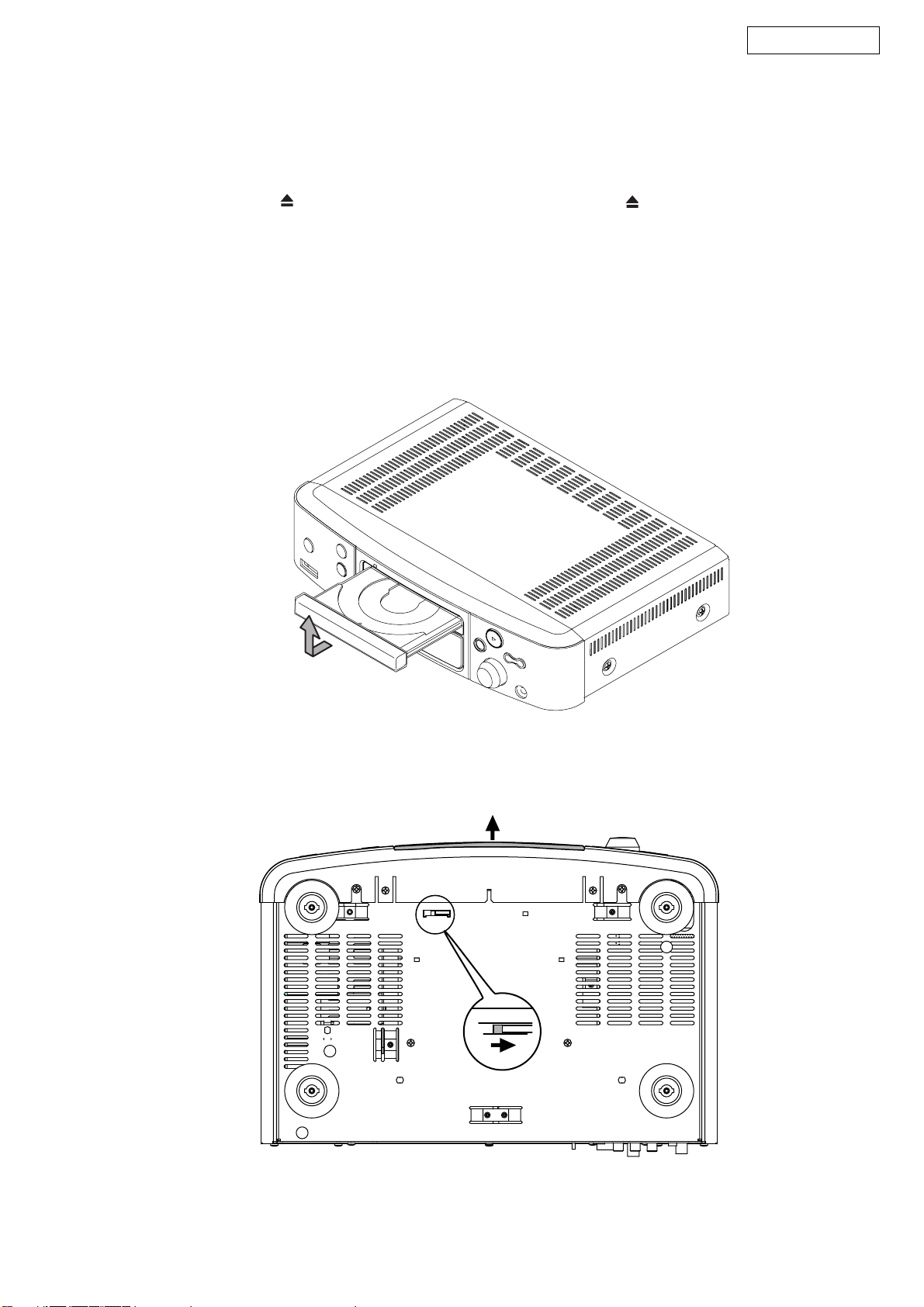
S-81/S-81DAB
DISASSEMBLY
(Follow the procedure below in reverse order when
reassembling.)
1. Loader Panel
(1) Switch on, and press [ (OPEN/CLOSE)] button
to open the Disc tray.
※ When a power supply is not turned on, insert a stick etc.
in the hole of a chassis bottom, it is made to slide in the
direction of an arrow, and a loader frame is pulled out.
(Refer to Fig. 2)
(2) Detach the Loader Panel by lifting.(Refer to Fig. 1)
(Refer to Fig. 1)
各部のはずしかた
(組み立てるときは、逆の順序でおこなってください。)
1. ローダーパネルのはずしかた
(1) 電源を入れ「 (OPEN/CLOSE)」ボタンを押して、
ディスクトレイを開きます。(Fig.1 参照 )
※電源が入らない場合はシャーシ底部の孔に棒等を
差し込み、矢印の方向へスライドさせてローダーフ
レームを引き出します。(Fig.2 参照)
(2) ローダーパネルを持ち上げてはずします。(Fig.1
参照 )
Fig.1
Fig.2
4
Page 5
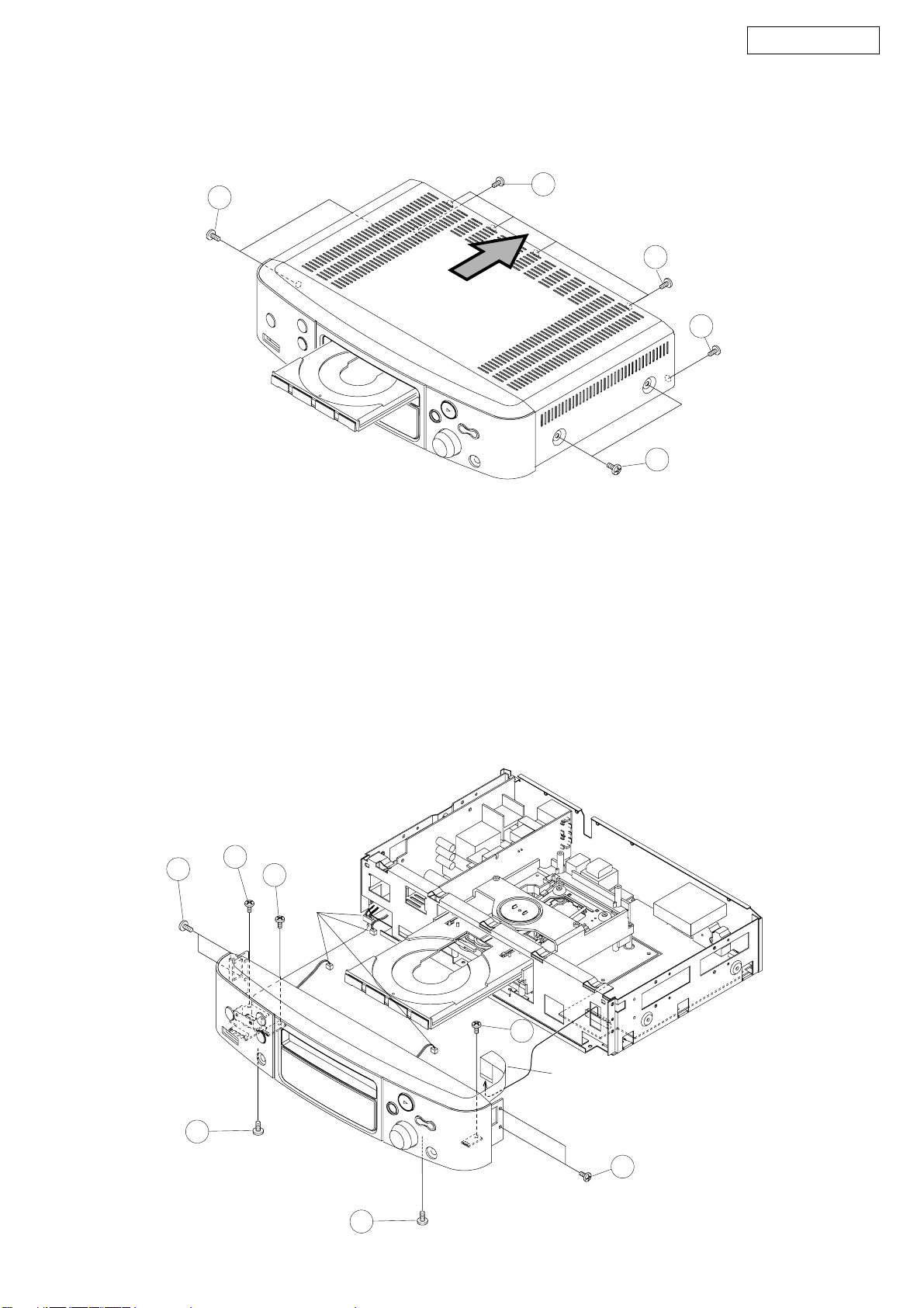
S-81/S-81DAB
2. Top Cover
(1) Remove 4 screws ① from the both sides.
(2) Remove 6 screws ② from the Rear Panel, then de-
tach the Top Cover to the arrow direction.
1
3. Front Panel
(1) Disconnect FFC coming out of the Front Panel.
(2) Disconnect 2 connecting cords coming out of the
Front Panel from the Main Unit, then disconnect 2
connecting cords coming out of the Main Unit from
the Front Panel.
(3) Remove 3 screws ③ fixing the Printed Wiring
Board of the Front Panel.
(4) Remove 2 screws ④ from the bottom side of the
Front Panel.
(5) Remove 4 screws ⑤ from the both sides of the
Front Panel, and then detachthe Front Panel.
2. トップカバーのはずしかた
(1) 両サイドから①のネジ 4 本をはずします。
(2) リアパネルから②のネジ 6 本をはずし、トップカ
バーを矢印の方向へはずします。
2
2
2
1
3. フロントパネルのはずしかた
(1) フロントパネルの FFC コードを本体からはずしま
す。
(2) フロントパネルのコネクタコード 2 本を本体から
はずし、本体のコネクタコード 2 本をフロントパ
ネルからはずします。
(3) フロントパネルの基板を取り付けている③のネジ
3 本をはずします。
(4) フロントパネル下面の④のネジ 2 本をはずしま
す。
(5) フロントパネルの両サイドの⑤のネジ 4 本をはず
してフロントパネルをはずします。
5
3
3
Connecting
Cord
3
FFC Cable
4
5
4
5
Page 6
S-81/S-81DAB
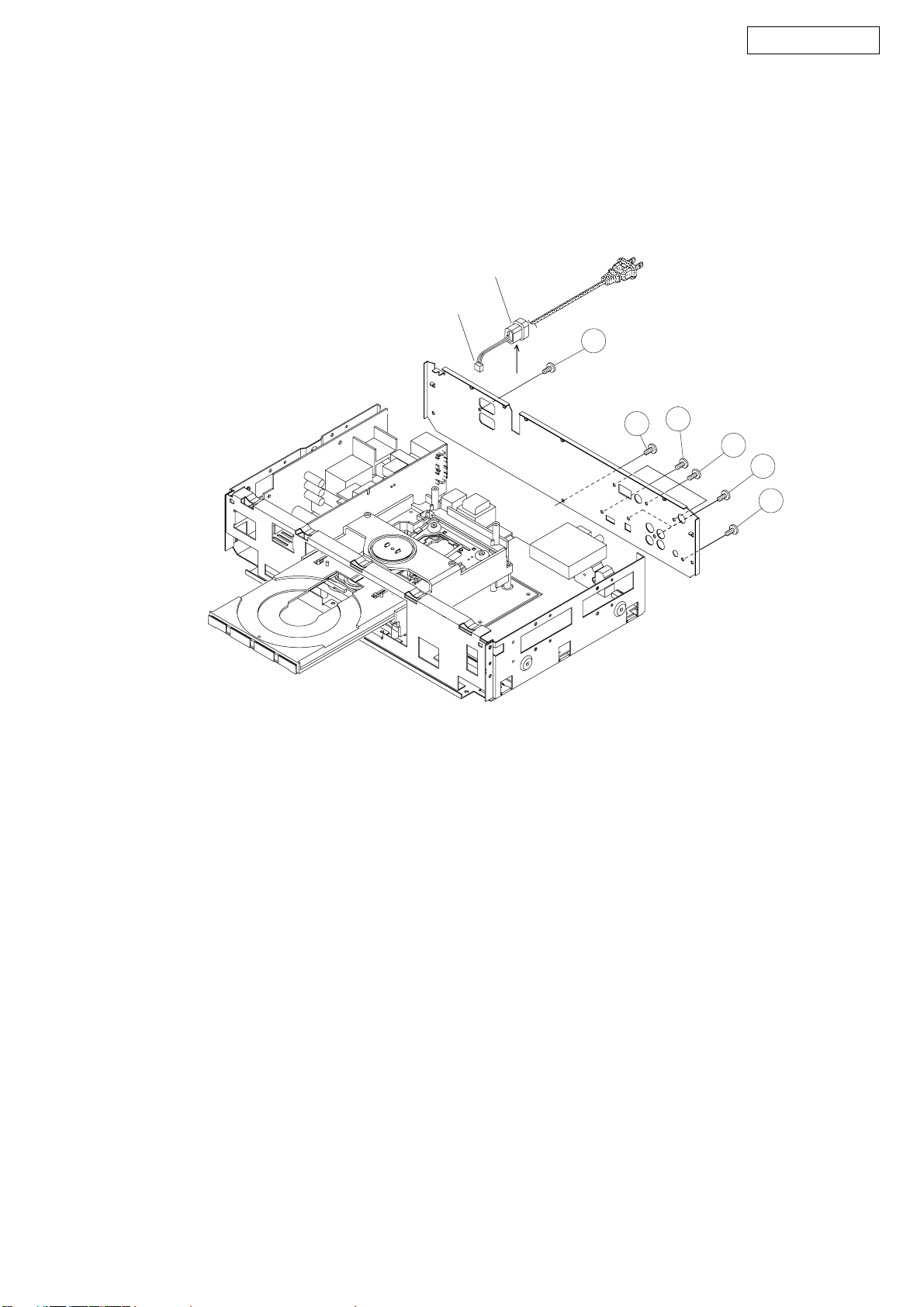
4. Rear Panel
(1) Disconnect the connector of AC cord, and detach
the cord bushing.
(2) Remove 3 ( or 5 in the case of U.S.A. & Canada
model ) screw ⑥ and 5 (or 6 in the case DAB U.K.
and Japan model ) screws ⑦ .
Connector
Cord Bush
4. リアパネルのはずしかた
(1) AC コードのコネクタとコードブッシュをはずし
ます。
(2) ⑥のネジ 3 本 (U.S.A.&Canada モデルの場合 :5
本)と⑦のネジ 5 本 (DABU.K. と日本モデルの場
合 :6 本)をはずします。
7
6
6
7
7
6
6
Page 7
S-81/S-81DAB
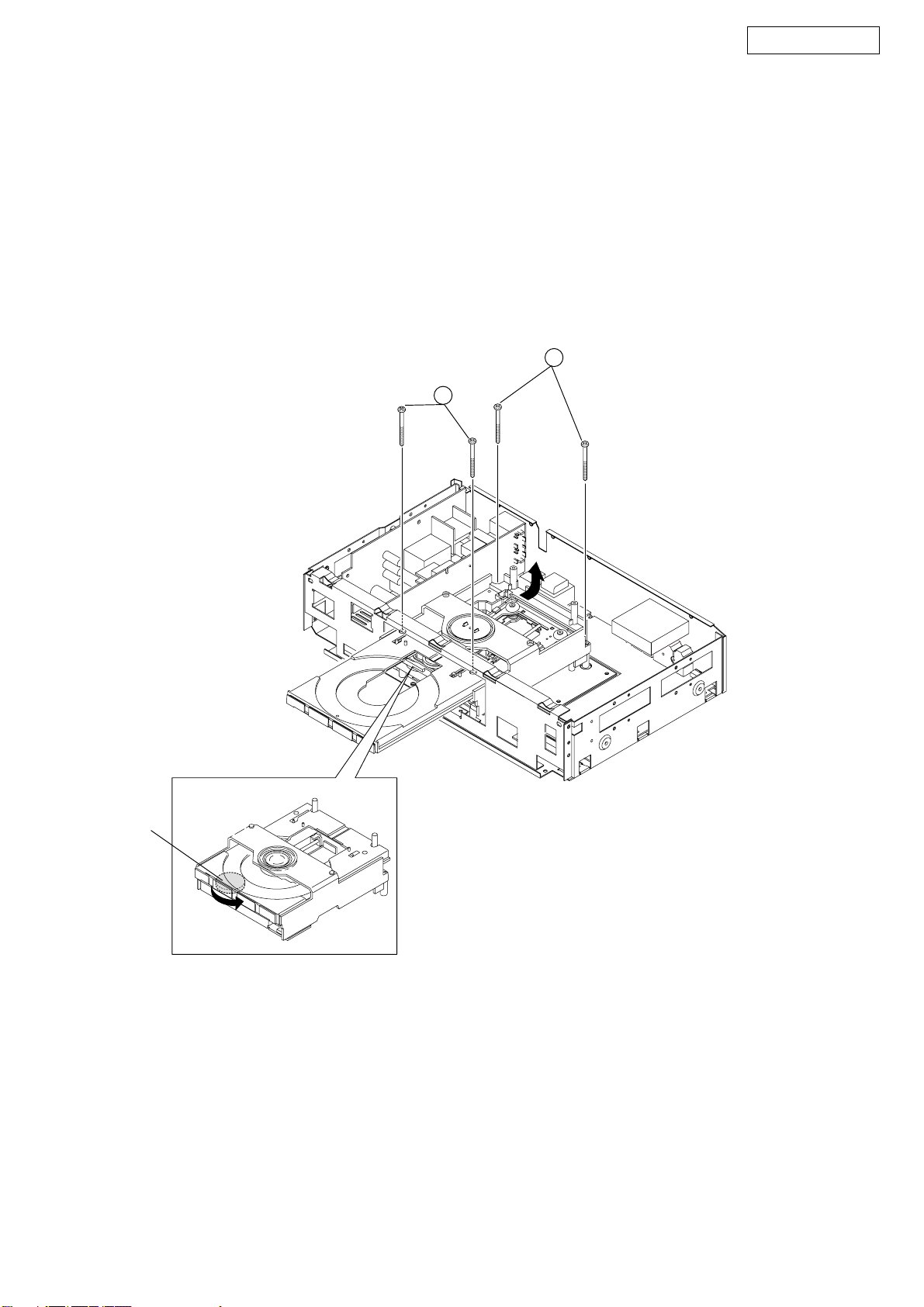
5. CD Mecha. Unit
(1) Open the Tray completely by turning the gear under
the Mecha. Unit counterclockwise.
(2) Remove 2 screws ⑧ on the Tray’s hole.
(3) Remove 2 rear screws ⑨ fixing the CD Mecha.
(4) Detach the CD Mecha. to the arrow direction.
(5) Lift the CD Mecha. and disconnect FFC and con-
nectors.
8
5. CD メカユニットのはずしかた
(1) メカユニットの下のギアを反時計方向に回して、
トレイを完全に開きます。
(2) トレイの孔から⑧のネジ 2 本をはずします。
(3) メカユニット後部から⑨のネジ 2 本をはずしま
す。
(4) メカユニットを矢印の方向にはずします。
(5) CD メカユニットを持ち上げ、コネクタと FFC を
はずします。
9
Gear
7
Page 8
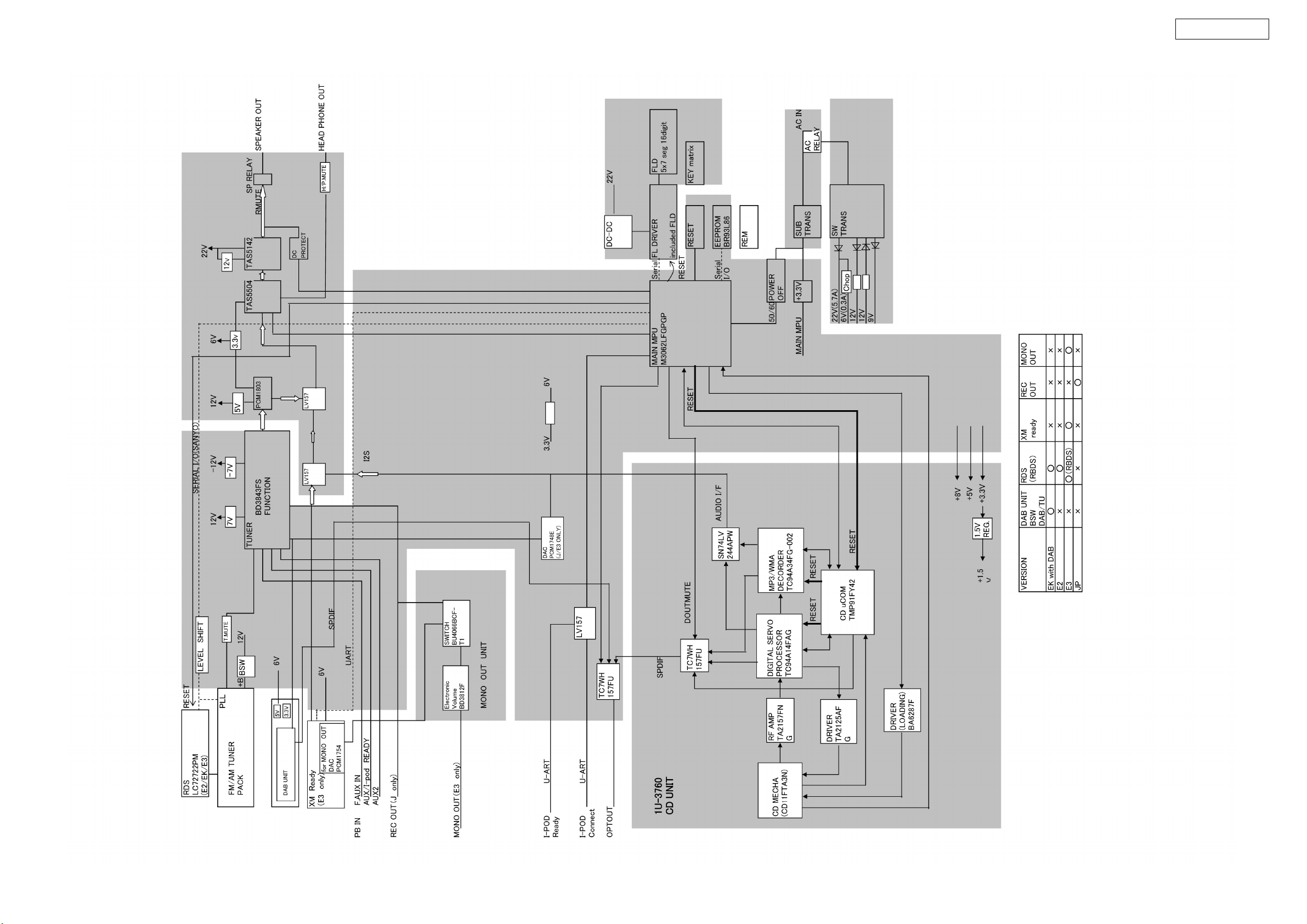
BLOCK DIAGRAM
S-81/S-81DAB
8
Page 9
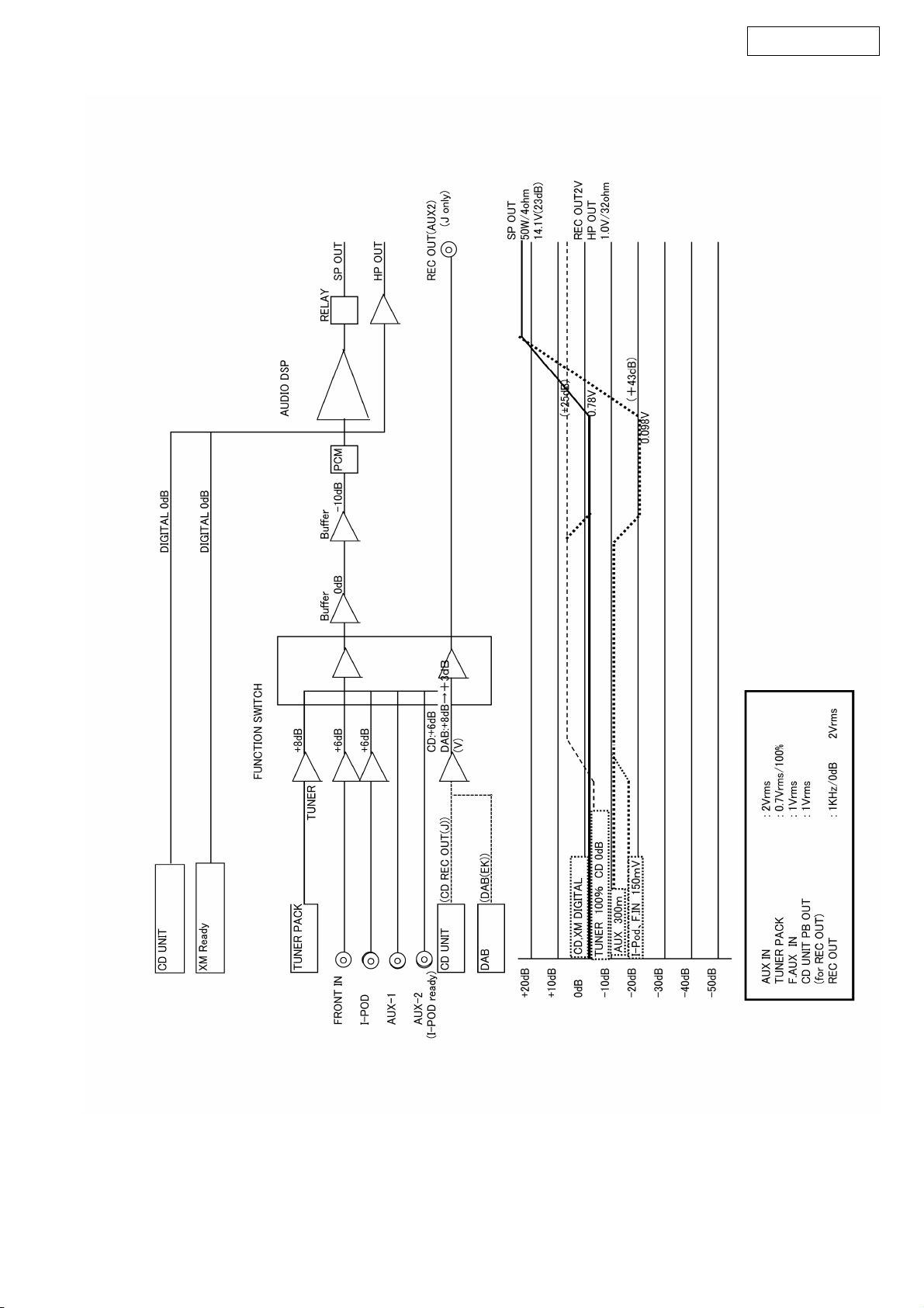
LEVEL DIAGRAM
S-81/S-81DAB
9
Page 10
S-81/S-81DAB
CD TEST MODE
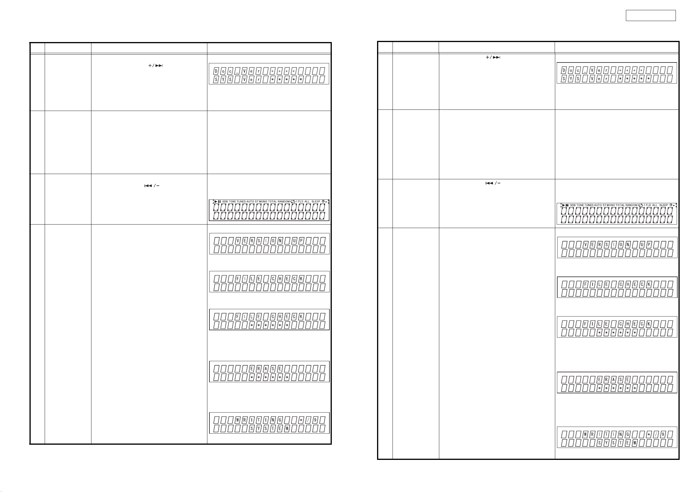
No
S1
S1.2
S2
Button name
Version No. of
iPod Dock andMain MPU Display Mode
EEPROM testing
Mode
FLD(VFD) checking mode
Function Display
・Plug AC cord into power outlet while pressing the
STOP button and the button same time
on Main Unit.
・The Version number of iPod Dock and Main MPU
is displayed.
・Unplug AC cord to clear this mode.
・When the version number is displayed, press
PLAY button on Main Unit.
the
・POWER LED illuminantes ORANGE to sign the
test mode started. MUTING ON.
・When power LED lighted BLUE, this EEPROM
test was OK.
・When power LED lighted RED, this EEPROM test
was NG.
・Unplug AC cord to clear this mode.
・Plug AC cord into power outlet while pressing the
PLAY button and the button same time on
Main Unit.
・All segment of FLD is turning on and off every
one second and all LED of Main unit’s button is
turned on. MUTING ON.
・Unplug AC cord to clear this mode.
・Plug AC cord into power outlet while pressing the
FUNCTION button and the CD STOP/BAND button same time on Main Unit.
・"VERSION UP” is displayed on the FL tube, then
the disc tray is opened.
・Load the disc containing the data for updating the
system microprocessor or CD microprocessor
version, then press the OPEN/CLOSE button on
Main Unit to start updating the version.
* The version update data is written on separate
discs.
++++ :The version number of iPod Dock
( When the iPod Dock is connected)
***** :The version number of Main MPU
・All segment turn off.
・All LED of Main unit’s button is turned on.
・All segment turn on and off.
・Version update mode
・Files being checked
・File checking completed
CD テストモード
No キー名称 機能 表示
・本体 STOP ボタンと ボタンを同時に押しなが
ら、AC コードをコンセントへ接続する .
iPodDock と
S1
メインマイコンの
バージョン表示モード
EEPROMTEST
S1.2
モード
FL(VFD) 管
S2
チェックモード
・iPodDock とメインマイコンの Ver を表示する.
MUTINGON.
・AC コードを抜くことによりモードを解除する.
・バージョン番号表示状態で、本体 PLAY ボタンを押
す.
・POWERLED が橙色に点灯する (TEST 開始 ).
MUTINGON.
・EEPROMTEST 後、OK の時は、青色に点灯す
る.
・EEPROMTEST 後、NG の時は、赤色に点灯す
る.
・AC コードを抜くことによりモードを解除する.
・本体 PLAY ボタンと ボタンを同時に押しなが
ら、AC コードをコンセントへ接続する.
・FL 管の全てを 2 秒周期で点滅 (1 秒点灯、1 秒
消灯 ) し、本体ボタンの LED を全点灯する.
MUTINGON.
・AC コードを抜くことによりモードを解除する.
・本体 FUNCTION ボタンと CDSTOP/BAND ボタンを
同時に押しながら,AC コードをコンセントへ接続す
る.
・FL 管に "VERSIONUP" を表示し、トレイが OPEN
する.
・SYSTEM マイコンまたは CD マイコンの VersionUp 用の
データが入った DISC を装着し、本体 OPEN/
CLOSE ボタンを押し、VersionUp を開始する.
※ VersionUp 用のデータは、別々のDISC に書か
れていること.
++++ :iPodDock の Ver 番号
(iPodDock 接続時)
***** :メインマイコンの Ver 番号
・全てのセグメントを消灯する.
・本体ボタンの LED を全点灯する.
・全てのセグメントを点灯・消灯する.
・VersionUp モード時
・ファイルチェック中
・ファイルチェック終了時
S3 Version Up mode
Main MPU : ****** : SYSTEM
CD : ****** : CD
・Old data being cleared
Main MPU : ****** : SYSTEM
CD : ****** : CD
・Version update data being written
Main MPU : * : writing counter (from 0 to 9)
10
S3 VERSIONUPモード
メインマイコンの場合:******:SYSTEM
CD の場合 :******: CD
・旧データ削除中
メインマイコンの場合:******:SYSTEM
CD の場合 :******: CD
・VersionUp データ書き込み中
メインマイコンの場合:* :書き込みカウンタ (0 〜 9)
Page 11
S-81/S-81DAB
No Button name Function Display
CD MPU : * : writing counter (from 000 to 100)
S3 Version Up mode
・When completing data writing
Main MPU : ****** : SYSTEM
CD : ****** : CD
・Plug AC cord into power outlet while pressing the
FUNCTION button and the OPEN/CLOSE button
same time on Main Unit.
・The system is reset, and once this is completed
the unit is set to the normal mode.
- Input Function : CD
- SDB : OFF
- BASS : 0
- TREBLE : 0
S4 Initialization mode
- DIMMER : 100%
- VOLUME : 0
- Preset Frequency of TUNER:
All 0
- TUNER’s -/+ button : -/+ button for TUNING
- CLOCK : 00:00(Flashing)
: AM12:00(Flashing)(E3)
- TIMER(EVERYDAY/ONCE):
Timer Function : CD
Timer start time : 0:00 (AM12:00 : E3)
Timer stop time : 0:00 (AM12:00 : E3)
・Plug AC cord into power outlet while pressing the
PLAY button and the button same time
on Main Unit.
・Turn the power on then set the volume level to 27
S5
DAB Function
CHECK Mode.
(For only S81DAB)
(-18dB).
・Set the function to "TUNER", the band to "DAB".
・Enable service reception without conducting DAB
auto scanning. (After about 10 to 15 seconds)
Receive frequency 12C : 227.360MHz
(Without switching the DISPLAY button) Signal
quality display
・Unplug AC cord to clear this mode.
・Plug AC cord into power outlet while pressing the
STOP button and the button same time
on Main Unit.
・ flashing
・Move the slide to the initially set position (10 mm
S6 CD service mode
towards the outside from the innermost position).
・Check by performing button input. Refer to S6.1
to S6.6.
**** : The version number of CD MPU
・Cancel the mode by turning the power back on.
・Input of buttons other than those used in this
mode is not guaranteed. (OK if malfunction
occurs)
No キー名称 機能 表示
CD の場合 :***:書き込みカウンタ
(% 表示:0 〜 100)
S3 VERSIONUPモード
・書き込み終了時
メインマイコンの場合:******:SYSTEM
CD の場合 :******: CD
・本体 FUNCTION ボタンと OPEN/CLOSE ボタンを同
時に押しながら,AC コードをコンセントへ接続する.
・初期化を行い、終了後、通常モードへ移行する.
-入力ファンクション : CD
-SDB : OFF
-BASS : 0
-TREBLE : 0
-DIMMER : 100%
-VOLUME : 0
S4 初期化
DABCHECK モード
S5
S-81DAB のみ)
(
S6 CD サービスモード
-チューナープリセット周波数 : 全て 0
-チューナー-/+ボタン : TUNING-/+ボタン
-時計 : 00:00( 点滅 )
:AM12:00( 点滅 )(E3)
-TIMER(EVERYDAY/ONCE):
タイマーファンクション : CD
タイマースタート時刻 : 0:00
:AM12:00(E3)
タイマーストップ時刻 : 0:00
:AM12:00(E3)
・本体 PLAY ボタンと ボタンを同時に押しな
がら、AC コードをコンセントへ接続する.
・POWERON 後、VOLLEVEL を 27(-18dB) とす
る.
・Function を TUNER、 BAND を DAB にする。
・DAB の AUTOSCAN を行わずにサービスの受信が
可能となる.(約 10 〜 15 秒後)
周波数 12C:227.360MHz を受信.
(DISPLAY キー切り替えずに)SignalQuality 表
示.
・AC コードを抜くことによりモードを解除する.
・本体 STOP ボタンと ボタンを同時に押しな
がら、AC コードをコンセントへ接続する.
・スライドを初期設定位置に移動する.(最内周か
ら外側 10mm の位置)
・ボタン入力によりチェックを行う.S6.1 〜 S6.6 参
照.
・電源の再投入によりモードを解除する.
・このモードで使用するボタン以外の入力は保証し
ない.(異常な動作になってもよしとする)
・ を点滅
****:CD マイコンの Ver 番号
11
Page 12
S-81/S-81DAB
No Button name Function Display
・Press the CD OPEN/CLOSE button to open the
tray.
Continue S6 display
・Set a disc on the tray, then press the CD OPEN/
6.1 Disc loading
CLOSE button again to close the tray. The disc is
mounted automatically.
・Move the slide to the initially set position (10 mm
towards the outside from the innermost position)
and stop in this status.
・Press the CD PLAY/PAUSE button. Execute the
following steps.
・ flashing
①
①LD ON (with servo still stopped)
②FOCUS ON (disc rotation, tracking off)
If no disc loaded, retry then stop.
③CLV ON
②
④TRACKING ON
⑤SUB CODE readout (playback sound output)
⑥When display is as in ⑤ and the PLAY button
is pressed, conduct BER (Block Error Rate)
display for 2 seconds. (Display total no.
generated in 10 seconds.)
③
* Press the PLAY button continuously for over 1
second to switch directly to SUB CODE
6.2 Servo check
readout in step
⑤ .
④
No キー名称 機能 表示
6.1 ディスク装着
6.2 サーボチェック
・CDOPEN/CLOSE ボタンでトレイを開く.
・ディスクを置き、再度 CDOPEN/CLOSE ボタンでトレイ
を閉じるとディスクをチャッキングする.
・スライドを初期設定位置(最内周から外側
10mm の位置)に移動し、その状態でストップ
する.
・CDPLAY/PAUSE ボタンを押すと下記ステップを実
行する.
①LDON( サーボ停止のまま )
②FOCUSON( ディスク回転、トラッキング OFF)
ディスク無しの場合、リトライ後停止する.
③CLVON
④TRACKINGON
⑤SUBCODE 読み出し(再生音出力)
⑥⑤の表示時に PLAY ボタンを押すと、2 秒間
BER(BlockErrorRate) の表示を行なう.
(10 秒間の間に発生した総数を表示)
* PLAY ボタンの 1 秒以上押し続けにて、ダイレクト
に⑤の SUBCODE 読み出しステップに移行する.
S6 の表示を継続する.
・ を点滅
①
②
③
④
6.3 Pickup movement
6.4 Stop
6.5 All servo on
・In the stop mode, pickup moves in REV (inwards)
or FWD (outwards) direction when the
button or the button pressed.
・When the button pressed, move to stop
operation after detection that inner switch has
turned on.
・Pickup movement stops when button released.
(Pickup moves while button is pressed.)
・When the STOP button is pressed, play operation
and servo stop.
・
After stopping, conduct reading of auto adjust values.
・When the FUNCTION button is pressed for over
2 seconds, all servos turn on, auto adjustment is
performed and switch to playback operation.
(Playback sound output)
⑤
@@ : T.No
XX:XX : Time
⑥
###### : B.E.R.
Continuous display of previous time
・Same as S6.
・ flashing
@@ : T.No
XX:XX : Time
6.3 ピックアップ移動
6.4 停止
6.5 全サーボ ON
・ストップ状態で ボタンまたは ボタンを
押すと、ピックアップが REV( 内周側 ) または
FWD( 外周側 ) 方向に移動する.
・ ボタンを押した時は、内周 SW の ON を
検出後ストップ動作に移行する.
・ボタンを離すとピックアップの移動を停止する.
( ボタンが押されている間、移動する.)
・STOP ボタンを押すと、PLAY 動作及びサーボを停
止する.
・停止後、自動調整値の読込みを行なう.
・FUNCTION ボタンを 2 秒以上の長押しすると全
サーボを ON し、自動調整を行なって再生動作
に移行する.(再生音出力)
⑤
@@ :T.No
XX:XX :時間
⑥
###### :B.E.R.
前回の表示を継続する.
・S6 と同じ.
・ を点滅
@@ :T.No
XX:XX :時間
12
Page 13
S-81/S-81DAB
No Button name Function Display
・When the the FUNCTION button is pressed for
under 2 seconds, the adjustment values are
displayed in the following order.
・ flashing
①
① FOCUS BALANCE
② FOCUS GAIN
③ TRACKING BALANCE
④ TRACKING GAIN
⑤ FOCUS OFFSET
XX : Adjustment value
②
⑥ TRACKING OFFSET
⑦ RFRP
⑧ Return to ① .
(NOTE) If auto adjustment is not completed,
proper values are not displayed.
XX : Adjustment value
③
XX : Adjustment value
④
Adjustment value
6.6
display
No キー名称 機能 表示
・FUNCTION ボタンを押す(2秒以上の長押しで
ない)と、下記の順番で調整値を表示する.
① FOCUSBALANCE
② FOCUSGAIN
③ TRACKINGBALANCE
④ TRACKINGGAIN
⑤ FOCUSOFFSET
⑥ TRACKINGOFFSET
⑦RFRP
⑧①に戻る。
( 注 ) 自動調整を終了して無い場合は正常な値が
表示されない.
6.6 調整値の表示
・ を点滅
①
XX :調整値
②
XX :調整値
③
XX :調整値
④
7 CD heat run mode
・Plug AC cord into power outlet while pressing the
ON/STANDBY button and the FUNCTION button
same time on Main Unit. (Be sure to insert the
CD before this operation.)
・Switches to mode according to button input.
See S7.1 and S7.2.
・If an error occurs, display the error and stop
operation at that point. Number of operations
held. See S7.3 to S7.5.
・Heat run no. cleared when the STOP button
pressed.
・Mode canceled and tray opened after the CD
OPEN/CLOSE button pressed.
・Unplug AC cord to clear this mode too.
XX : Adjustment value
⑤
XX : Adjustment value
⑥
XX : Adjustment value
⑦
XX : Adjustment value
・ lit
・Normal display except when lit.
7 CD ヒートランモード
・ディスクを入れた状態で本体 ON/STANDBY ボタン
と FUNCTION ボタンを同時に押しながら、
AC コードをコンセントへ接続する.
・ボタン入力に応じたモードへ移行する.S7.1 〜
S7.2 参照.
・エラーが発生したら、エラー表示をしてその場で動
作を停止する。動作回数は保持しておく.
S7.3 〜 S7.5 参照.
・STOP ボタンを押した場合、ヒートラン回数をクリアす
る.
・CDOPEN/CLOSE ボタンが押されたら、モードを解
除してトレイをオープンする.
・AC コードを抜くことでもモードを解除する.
XX :調整値
⑤
XX :調整値
⑥
XX :調整値
⑦
XX :調整値
・ を点灯
・ を点灯している以外は通常と同じ表示.
13
Page 14
S-81/S-81DAB
No Button name Function Display
・The CD heat run mode is launched. Once writing
of the TOC data is completed, press the CD
PLAY/PAUSE button. Count this as the 0th heat
run repetition.
① Play from the first to last track on disc.
・ lit
① , ②
・In cases other than when is lit, same display as
during normal playback.
② If disc being used has less than 20 tracks, play
all tracks. If disc has 21 or more tracks, skip to
final track after playback of first track has
finished.
③ After disc playback has finished, move pickup
Normal heat run
7.1
mode
to innermost position and open tray.
④ When loader open status detected, close tray
again, re-read TOC and start playback from
the first track on the disc.
③
⑤ The heat run repetition no. is incremented
(increased by 1) when the tray is opened.
Automatic
7.2
mounting mode
⑥ Conduct ① to ⑤ repeatedly.
・After CD heat run mode has started and reading
the TOC has finished, press the CD STOP/
BAND button once in the stop mode.
・TOC reading ⇒ Search for first track on disc ⇒
tray open ⇒ tray close ⇒ TOC reading ⇒
repeat. No. heat run repetitions displayed on
time display section.
XXXX : No. of heat run repetitions
④
While tray opened
・Same as for regular heat run. See 7.1 ③ .
When tray closed
・Same as for regular heat run. See 7.1. ④
・Increment the heat run repetition no. (increase by
1) at the point when the loader has finished
opening.
No キー名称 機能 表示
7.1 通常ヒートランモード
7.2 チャッキングモード
・CDヒートランモードが起動し、TOCREAD が完了し
た後、CDPLAY/PAUSE ボタンを押す.この時、
ヒートラン繰り返し回数を 0 回目とする.
①ディスクの先頭トラックから最終トラックまで再生す
る.
②使用ディスクが 20 トラック以内の場合は全トラックを
再生する.21 トラック以上なら1トラック目終了後、
最終トラックにスキップする.
③ディスクの再生終了後、ピックアップを最内周に移
動させトレイを開く.
④ローダー OPEN 状態を検出したら、再度トレイを
閉じ再度 TOC を読み取り後、ディスクの先頭
トラックから再生を開始する.
⑤ヒートラン回数はトレイを OPEN したところで
インクリメント ( ヒートラン回数を 1 つ増やす ) する.
⑥①〜⑤を繰り返し実行する.
・CDヒートランモードが起動し、TOCREAD が完了し
た後、停止中に CDSTOP/BAND ボタンを 1 回押
す.
・TOC 読込み⇒ディスクの先頭トラックをサーチ⇒
トレイ OPEN ⇒トレイ CLOSE ⇒ TOC 読込み⇒を繰り
返す。時間表示部にヒートランの繰り返し回数を表
示する。
・ヒートラン回数はローダーを OPEN し終えたところで
インクリメント ( ヒートラン回数を 1 つ増やす ) する.
・ を点灯
①、②
・ を点灯している以外は通常再生中と同じ表示.
③
XXXX :ヒートラン繰り返し回数
④
トレイオープン中
・通常ヒートラン時と同じ.S7.1③を参照
トレイクローズ中
・通常ヒートラン時と同じ.S7.1④を参照
14
Page 15
S-81/S-81DAB
No Button name Function Display
7.3 Error display
E1-00 : Disc cannot be detected
E1-01 : Tracking offset adjustment not possible
E1-02 : Focus offset adjustment not possible
E2-00 : Focus servo could not follow during
playback
E2-01 : Focus servo could not follow during
searching
E2-03 : Focus servo could not follow during TOC
reading
E2-05 : Focus servo could not follow during
pause
E2-10 : Subcode can no longer be read during
playback
E2-11 : Subcode can no longer be read during
searching
E2-12 : Subcode can no longer be read during
TOC reading
E2-14 : Subcode cannot be read during pause
E2-15 : Subcode cannot be read during manual
search
E3-00 : TOC could not be read within specified
time
E3-01 : PVD/SVD analysis could not be
completed within specified time
E4-04 : Search time out (searching not
completed within specified time)
E4-05 : Decoder bus (Error in communications
with CD decoder)
E5-00 : Inner switch not on
E6-00 : Inner switch not off
E9-00 : Error in CD microprocessor
E9-01 : Other error
・Press the button while the error is
displayed.
・ lit
X-XX : Error display
・ lit
・ No. heat runs is displayed for 5 seconds, the
Error display
7.4
switching (1)
error display reappears.
XXXX : No. of heat run repetitions
・Error display reappears after 5 seconds. See S7.3.
Error display
7.5
switching (2)
・Press the button while the error is
displayed.
・ The track no. and time when the error occurred is
displayed for 5 seconds, then error display
reappears.
・In cases other than when is lit, same display as
during normal playback.
No キー名称 機能 表示
7.3 エラー表示
7.4 エラー表示の切換 (1)
7.5 エラー表示の切換 (2)
E1-00:ディスク検出出来ず
E1-01:トラッキングオフセット調整出来ず
E1-02:フォーカスオフセット調整出来ず
E2-00:再生中フォーカスサーボが追従できなかった
時があった
E2-01:サーチ中フォーカスサーボが追従できなかった時
があった
E2-03:TOC 読み込み中フォーカスサーボが追従でき
なかった時があった
E2-05:ポーズ中フォーカスサーボが追従できなかった
時があった
E2-10:再生中サブコードが読めなくなった
E2-11:サーチ中サブコードが読めなくなった
E2-12:TOC 読み込み中サブコードが読めなく
なった
E2-14:ポーズ中サブコードが読めない
E2-15:マニュアルサーチ中サブコードが読めない
E3-00:TOC 規定時間以内に読めず
E3-01:PVD/SVD 解析規定時間以内に終わらず
E4-04:サーチタイムアウト(サーチが規定時間内に終了しな
かった )
E4-05:デコーダバス (CDDECODER との通信エラー
が発生した )
E5-00:内周 SWON せず
E6-00:内周 SWOFF せず
E9-00:CD マイコンエラーが発生
E9-01:その他のエラーが発生
・エラー表示中に キーを押す.
・ヒートラン回数を 5 秒間表示し、エラー表示に戻る.
・エラー表示中に キーを押す.
・発生時のトラック番号と時間を 5 秒間表示しエラー表
示に戻る.
・ を点灯
X-XX :エラー表示
・ を点灯
XXXX :ヒートラン繰り返し回数
・5 秒後にエラー表示に戻る.S7.3 参照
・ を点灯している以外は通常再生中と同様の表
示.
・Error display reappears after 5 seconds. See S7.3.
・5 秒後にエラー表示に戻る.S7.3 参照
15
Page 16
WAVEFORMS
S-81/S-81DAB
7
12
13
11
10
8
9
2
3
4
6
5
10
11
1U-3760 CD P.W.B. Unit component side
13
8
9
2
3
4
6
5
1
12
7
2
1U-3760 CD P.W.B. Unit foil side
16
2
Page 17
S-81/S-81DAB
17
Page 18
SEMICONDUCTORS
Only major semiconductors are shown, general semiconductors etc. are omitted to list.
主な半導体を記載しています。汎用の半導体は記載を省略しています。
1. IC’s
LC72722PM (IC102 : 1U-3761)
S-81/S-81DAB
Block Diagram
+5V +5V
Vdda
Vssa
MPXIN
REFERENCE
VOLTAGE
ANTIALIASING
FILTER
V
REF
57 kHz
BPF
(SCF)
REF
124V
SYR
223MPXIN CE
322Vdda DI
421Vssa CL
520FLOUT DO
619CIN
LC72722PM
RDS-ID
718T1 SYNC
817T2 T7(CORREC/ARI-ID/TA/BEO)
916T3(RDCL) T6(ERROR/57K/TP/BE1)
10 15T4(RDDA) Vssd
11 14T5(RSFT) Vddd
12 13X
OUT
SMOOTHING
FILTER
V
CINFLOUT
+
Ð
REF
X
IN
PLL
(57 kHz)
CLOCK
RECOVERY
(1187.5 Hz)
DATA
DECODER
Vddd
Vssd
RDS-ID
DO
CL
CE
T1
T2
T3 to T7
DI
CCB
TEST
RAM
(24 BLOCK DATA)
MEMORY CONTROL
ERROR CORRECTION
(SOFT DECISION)
CLK(4.332 MHz)
OSC/DIVIDER
X
IN
X
OUT
SYNC/EC CONTROLLER
SYNC
DETECT-1
SYNC
DETECT-2
SYNC
SYR
18
Page 19
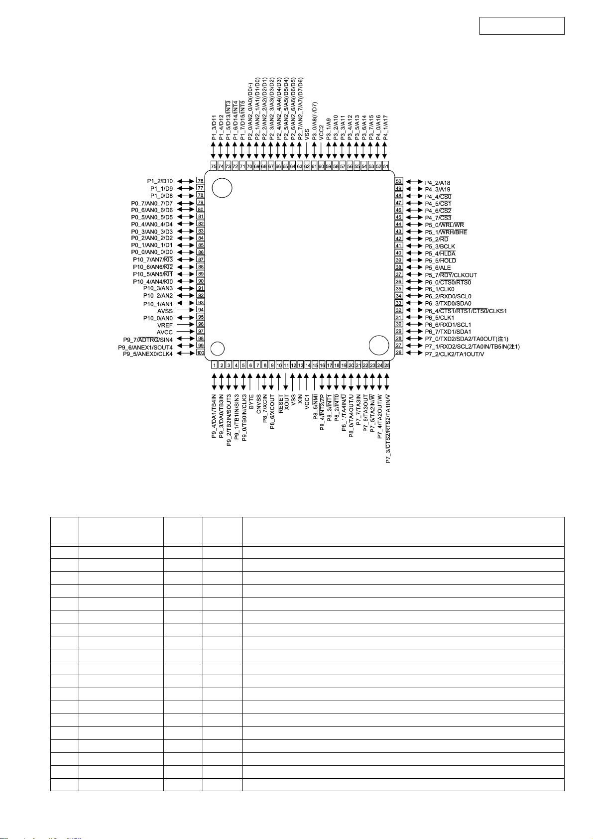
S-81/S-81DAB
Pin Functions
Pin No. Pin name Function I/O Pin circuit
Vdda
1 VREF Reference voltage output (Vdda/2) Output
Vssa
2 MPXIN Baseband (multiplexed) signal input Input
5 FLOUT Subcarrier output (filter output) Output
Ð
+
Vdda
6 CIN Subcarrier input (comparator input) Input
Vssa
3 Vdda Analog system power supply (+5 V) Ñ Ñ
4 Vssa Analog system ground Ñ Ñ
12 XOUT Crystal oscillator output (4.332/8.664 MHz) Output
13 XIN Crystal oscillator input (external reference signal input)
7 T1 Test input (This pin must always be connected to ground.) Input
8T2
9 T3 (RDCL) Test I/O (RDS clock output)
10 T4 (RDDA) Test I/O (RDS data output)
11 T5 (RSFT) Test I/O (soft-decision control data output)
16 T6 (ERROR/57K/TP/BE1)
17 T7 (CORREC/ARI-ID/TA/BE0)
18 SYNC Block synchronization detection output
Test input (standby control)
0: Normal operation, 1: Standby state (crystal oscillator stopped)
Test I/O (error status output, regenerated carrier output,
TP output, error block count output)
Test I/O (Error correction status output, SK detection output,
TA output, error block count output)
I/O*
X
X
IN
OUT
Vssd
Vdda
Vssa
V
REF
Vddd
Vssd
S
Vssd
A12365
A12366
A12367
A12368
A12369
A12370
A12371
19 RDS-ID RDS detection output
Output
20 DO Data output
21 CL Clock input
22 DI Data input
23 CE Chip enable
24 SYR Synchronization and RAM address reset (active high)
14 Vddd Digital system power supply (+5 V) Ñ Ñ
15 Vssd Digital system ground Ñ Ñ
Note: * Normally function as an output pin. Used as an I/O pin in test mode, which is not available to user applications.
Serial data interface (CCB)
Input
19
Vssd
S
Vssd
A12372
A12373
Page 20
M3062LFGPGP (IC103 : 1U-3761)
S-81/S-81DAB
PIN FUNCTION
Pin
No.
1 F.AUX_IN I - F.AUX connected/disconnected detection input (H : Connected)
2 FL_RESET O L Reset output to driver built into FL display tube
3 FLDA SO L Serial data output to driver built into FL display tube
4 NC O L Not used
5 FLCK CLK L Serial clock output to driver built into FL display tube
6 BYTE I - External data bus width switching input (GND : Single chip mode)
7 CNVSS I - Processor mode switching input (GND : Single chip mode, PULL DOWN)
8 NC O L Not used
9 NC O L Not used
10 RESET I - Reset input
11 XOUT O - Oscillator output (16MHz)
12 VSS - - GND
13 XIN I - Oscillator input (16MHz)
14 VCC1 - - Power supply
15 NMI INT - Not used (PULL UP)
16 /PROTECT INT - Speaker and driver IC error detection input
17 REQS INT - Communications request input from CD microprocessor
18 /IPOD_PROTECT I - i-Pod supply power error detection input
19 50/60 I - Supply power pulse input (50Hz / 60Hz)
Port Name I/O Initial Function
20
Page 21
S-81/S-81DAB
Pin
No.
20 REQH O L Communications request output to CD microprocessor
21 XM_COMMAND O L Not used (XM ready command output)
22 XM_REQ I - Not used (XM ready REQUEST terminal)
23 VOL_JOGB I - JOG pulse input B for VOL
24 VOL_JOGA I - JOG pulse input A for VOL
25 FLCS O L Chip selection output to driver built into FL display tube
26 MSCLK CLK L Communications serial clock output to CD microprocessor
27 MDO RXD - Communications serial clock input from CD microprocessor
28 MDI TXD L Communications serial data output to CD microprocessor (Nch open Drain -
29 IS1_DIN TXD L i-Pod READY/CONNECT comunications output (UART)
30 IS1_DOUT RXD - i-Pod READY/CONNECT comunications input (UART)
31 IPOD_SEL O L i-Pod READY/CONNECT switching output (H : READY, L: CONNECT)
32 XM_RESET O L XM ready RESET output
33 XM_MOXMI TXD L XM ready comunications input (UART)
34 XM_MIXMO RXD L XM ready comunications output (UART)
35 XM_POWER O L XM ready power control output
36 PWRON_CD O L CD unit power control output
37 /CDRESET O L Reset output to CD microprocessor
38 H/P_SW I - Headphones connected/disconnected detection input
39 LED_DA O L DATA output to LED driver (BU2090F)
40 E2P_CLK O L Clock output to EEPROM
41 E2P_DO I - Data input from EEPROM
42 E2P_DI O L Data output to EEPROM
43 E2P_CS O L Chip selection output to EEPROM
44 LED_CK O L CLOCK output to LED driver (BU2090F)
45 NC O L Not used
46 PWB_CHECK I - PWB checking mode input (PULL DOWN)
47 PWB_CHECK I - PWB checking mode input (PULL DOWN)
48 PWB_CHECK I - PWB checking mode input (PULL DOWN)
49 PWB_CHECK I - PWB checking mode input (PULL DOWN)
50 REC_MUTE O L REQ MUTE terminal (H : MUTE)
51 CL O L MONO_OUT electronic volumu clock output (BD3812F)
52 EMPHASIS_IN I - Emphasis signal input
53 SP_DETECT I - SP connected/disconnected detection input (H : SP Connected)
54 CLOCK_SEL1 O L Master clock audio data selection output 1 (selection 1 : selection XM and CD)
55 CLOCK_SEL2 O L Master clock audio data selection output 2 (Selection selection 1 output and AD
56 SP_RL O L Relay output (L : MUTE)
57 SEL_CLK O L Input SELECTOR (BD3843FS) clock signal
58 SEL_DATA O L Input SELECTOR (BD3843FS) data latch output
59 DA O L Electronic volumu (BD3812FS) data latch output
60 VCC2 - - Power supply
61 H/P_MUTE O L Headphone MUTE output (L : MUTE ON)
62 VSS - - GND
63 P.ON/OFF O L Overall product power ON/OFF (standby) output
64 STEREO I - Tuner stereo signal detection input
65 /TUNED I - Tuner reception detection input
66 T.MUTE O L Tuner MUTE output
67 SANYO_CE O L Chip enable output to tuner PLL/RDS IC
68 SANYO_DI O L Data output to tuner PLL/RDS IC
69 SANYO_CLK O L Clock output to tuner PLL/RDS IC
70 SANYO_DO I - Data input from tuner PLL/RDS IC
71 WAKE INT - Button accept interrupt input (for resetting from low power consumption mode)
72 TU_POWER O L Tuner power ON/OFF control (H : Tuner ON)
73 REMOTE INT - IR remote controller input
Port Name I/O Initial Function
PULL UP)
converter output)
21
Page 22
S-81/S-81DAB
Pin
No.
74 /SYR O L Reset output to tune RDS's IC
75 DOUTMUTE O L D.OUT MUTE output ( H : MUTE)
76 CLSW I - CD MECHA. CLOSE SW detection input
77 OPSW I - CD MECHA. OPEN SW detection input
78 SEL O L MONO_OUT signal selection output
79 OPEN O L OPEN control signal output to loading driver (BA6287F)
80 CLOSE O L CLOSE control signal output to loading driver (BA6287F)
81 VR_DSP_CLOCK O L Clock output to digital audio PWM processor (TAS5504)
82 VR_DSP_DATA O L Data output to digital audio PWM processor (TAS5504)
83 DSP_MUTE O L Mute output to digital audio PWM processor (TAS5504)
84 DSP_RESET O L Reset output to digital audio PWM processor (TAS5504)
85 H/P_SEL O L H/P selection signal output to digital audio PWM processor (TAS5504) (L : H/P-
86 /DSP_PDN O L Power down control output to digital audio PWM processor (TAS5504) (L :
87 ROM_CORRECTI
88 USA/EURO/
89 IPOD_FUNC I (AD) - iPod type selection inpu (CONNECT : 0 to 1.1V, READY : 1.2 to 2.2V, APPLE :
90 DIMMER O L Not used (as DIMMER detection input, output port setting)
91 XM/DAB/NO I (AD) - Product type selection input (NO : 0 to 1.1V, DAB : 1.2 to 2.2V, XM : 2.3 to 3.3V)
92 RDS I - RDS YES/NO selection input (H : YES, L : NO)
93 KEY0 I (AD) - Main unit's operating button detection input
94 AVSS - - GND for AD converter
95 KEY1 I (AD) Main unit's operating button detection input
96 VREF - - Reference voltage input for AD converter and DA converter
97 AVCC - - Power supply of AD converter
98 IPOD_CONNECT I - i-Pod connected/disconnected detection input (L : Connected)
99 IPOD_ID O L i-Pod ID (Accessory) ON/OFF switching output (H : ON)
100 IPOD_CHARGE O L i-Pod power supply ON/OFF control output
Port Name I/O Initial Function
ON & SP_OUT-OFF)
Power down)
I - Not used (PULL UP)
ON
I - Product destination selection input (JAPAN : 0 to 1.1V, EURO : 1.2 to 2.2V, USA
JAPAN
: 2.3 to 3.3V)
2.3 to 3.3V)
22
Page 23
PCM1748E (IC201 : 1U-3761)
BCK
DATA
LRCK
DGND
V
V
V
OUT
V
OUT
1
2
3
4
5
DD
6
CC
7
L
8
R
PCM1748E
16
SCK
15
ML
14
MC
13
MD
12
ZEROL/NA
11
ZEROR/ZEROA
10
V
COM
9
AGND
S-81/S-81DAB
PIN ASSIGNMENTS
PIN NAME TYPE FUNCTION
1 BCK IN Audio Data Bit Clock Input.
2 DATA IN Audio Data Digital Input.
3 LRCK IN L-Channel and R-Channel Audio Data Latch En-
able Input.
(1)
4 DGND - Digital Ground
5V
6V
7V
OUT
8V
OUT
- Digital Power Supply, +3.3V
DD
- Analog Power Supply, +5V
CC
L OUT Analog Output for L-Channel.
R OUT Analog Output for R-Channel.
9 AGND - Analog Ground
10 V
COM
- Common Voltage Decoupling.
11 ZEROR/ OUT Zero Flag Output for R-Channel/Zero Flag Output
ZEROA for L/R-Channel.
12
ZEROL/NA
OUT Zero Flag Output for L-Channel/No Assign.
13 MD IN Mode Control Data Input.
14 MC IN Mode Control Clock Input.
15 ML IN Mode Control Latch Input.
16 SCK IN System Clock Input.
NOTES: (1) Schmitt-trigger input, 5V tolerant. (2) Schmitt-trigger with internal
pull-down, 5V tolerant.
(1)
(1)
(2)
(2)
(2)
BCK
LRCK
DATA
ML
MC
MD
SCK
BLOCK DIAGRAM
Serial
Input
I/F
Function
Control
I/F
System Clock
System Clock
Manager
8x
Oversampling
Digital Filter
with
Function
Controller
Enhanced
Multi-Level
Delta-Sigma
Modulator
Zero Detect
DAC
DAC
Output Amp and
Low-Pass Filter
Output Amp and
Low-Pass Filter
Power Supply
V
L
OUT
V
COM
V
R
OUT
ZEROL
ZEROR
23
V
DD
DGND
V
CC
AGND
Page 24
BD3843FS (IC202 : 1U-3761)
S-81/S-81DAB
24
Page 25
BA6287F (IC301 : 1U-3760)
TMP91FY42 (IC302 : 1U-3760)
S-81/S-81DAB
25
Page 26
PIN DESCRIPTIONS
S-81/S-81DAB
Pin
No.
1 VREFL VREFL - - GND (AD converter VREFL)
2 AVSS AVSS - - GND
3 AVCC AVCC - - +3.3V
4 P70/TA0IN - O L Not used
5 P71/TA1OUT - O L Not used
6 P72/TA3OUT - O L Not used
7 P73/TA4IN - O L Not used
8 P74/TA5OUT - O L Not used
9 P75/TA7OUT - O L Not used
10 P80/TB0IN0/INT5 34REQ I - Request input from TC94A34FG(MP3/WMA DECORDER)
11 P81/TB0IN1/INT6 REQH I - Request input from System ucom
12 P82/TB0OUT0 REQS O L Request output to System ucom
13 P83/TB0OUT1 - O L Not used
14 P84/TB1IN0/INT7 PWRON_CD I - Power ON/OFF switching input from System ucom
15 P85/TB1IN1/INT8 - O L Not used
16 P86/TB1OUT0 - O L Not used
17 P87/TB1OUT1 - O L Not used
18 P90/TXD0 MDO O L Serial Data output to System ucom
19 P91/RXD0 MDI I - Serial Data input from System ucom
20 P92/SCLK0/CTS0
21 P93/TXD1 TXD O L Use for the WRITING
22 P94/RXD1 RXD I - Use for the WRITING
23 P95/SCLK1/CTS1
24 AM0 AM0 I - Fixed to H (+3.3V)
25 DVCC DVCC - - +3.3V
26 X2 X2 O - Oscillator output (27MHz)
27 DVSS DVSS - - GND
28 X1 X1 I - Oscillator input (27MHz)
29 AM1 AM1 I - Fixed to H (+3.3V)
30 RESET
31 P96/XT1 - O L Not used
32 P97/XT2 - O L Not used
33 EMU0 EMU0 O - Non connection
34 EMU1 EMU1 O - Non connection
35 PA0/INT1 - O L Not used
36 PA1/INT2 - O L Not used
37 PA2/INT3 - O L Not used
38 PA3/INT4 - O L Not used
39 PA4 - O L Not used
40 PA5 - O L Not used
41 PA6 - O L Not used
42 PA7 - O L Not used
43 ALE - O L Not used
44 P00/AD0 MODE0 I - MODEL SELECT
45 P01/AD1 MODE1 I - MODE0:1 L:L=S81(J/E3) / L:H=S81(E2) / H:H=DCDF102(ALL)
46 P02/AD2 - O L Not used
47 P03/AD3 - O L Not used
48 P04/AD4 DAC_CS O H Mode control latch output to PCM1748E(DAC)
49 P05/AD5 - O L Not used
50 P06/AD6 DAC_RST O L Reset output to DAC (RESERVE)
51 P07/AD7 DAC_MDI O L Mode control data output to PCM1748E(DAC)
52 P10/AD8/A8 DAC_MCK O L Mode control clock output to PCM1748E(DAC)
53 P11/AD9/A9 - O L Not used
54 P12/AD10/A10 - O L Not used
55 P13/AD11/A11 EMPHASIS O L Emphasis output to System ucom
56 P14/AD12/A12 - O L Not used
57 P15/AD13/A13 - O L Not used
58 P16/AD14/A14 - O L Not used
59 P17/AD15/A15 34RESET O L Reset output to TC94A34FG(MP3/WMA DECORDER)
Pin Name Symbol I/O Initial Function
MSCLK I - Serial Clock input from System ucom
- O L Not used
CDRESET I - Reset input from System ucom
26
Page 27
S-81/S-81DAB
Pin
No.
60 P20/A0/A16 34STANBY O L Standby control output to TC94A34FG(MP3/WMA DECORDER)
61 P21/A1/A17 34SRMSTB O L SRAM Standby control output to TC94A34FG(MP3/WMA DECORDER)
62 DVSS DVSS - - GND
63 NMI
64 DVCC DVCC - - +3.3V
65 P22/A2/A18 - O L Not used
66 P23/A3/A19 DOUTSEL O L DOUT SELECT output to TC7WH157 ( L:CD-DA / H:MP3/WMA )
67 P24/A4/A20 - O L Not used
68 P25/A5/A21 14RESET O L Reset output to TC94A14FA(Servo DSP)
69 P26/A6/A22 14CCE O H Chip Enable output to TC94A14FA(Servo DSP)
70 P27/A7/A23 14BUCK O L Serial Clock output to TC94A14FA(Servo DSP)
71 P30/RD
72 P31/WR
73 P32/HWR
74 P33/WAIT
75 P34/BUSRQ
76 P35/BUSAK
77 P36/R/W
78 P37/BOOT
79 P40/CS0
80 P41/CS1
81 P42/CS2
82 P43/CS3
83 P60/SCK - O L Not used
84 P61/SO/SDA 34MIDIO I/O L Data I/O to TC94A34FG(MP3/WMA DECORDER)
85 P62/SI/SCL 34MICK O L Clock output to TC94A34FG(MP3/WMA DECORDER)
86 P63/INT0 - O L Not used
87 P64/SCOUT - O L Not used
88 P65 - O L Not used
89 DVCC DVCC - - +3.3V
90 P66 - O L Not used
91 DVSS DVSS - - GND
92 P50/AN0 - I - Not used (Pull down)
93 P51/AN1 - I - Not used (Pull down)
94 P52/AN2 - I - Not used (Pull down)
95 P53/AN3/ADTRG
96 P54/AN4 - I - Not used (Pull down)
97 P55/AN5 - I - Not used (Pull down)
98 P56/AN6 - I - Not used (Pull down)
99 P57/AN7 LD_CHK I - Current check of LD
100 VREFH VREFH - - +3.3V (AD converter VREFH)
Pin Name Symbol I/O Initial Function
NMI I - Not used (Pull down)
- O L Not used
- O L Not used
14BUS3 I/O L DATA BUS to TC94A14FA(Servo DSP)
14BUS2 I/O L DATA BUS to TC94A14FA(Servo DSP)
14BUS1 I/O L DATA BUS to TC94A14FA(Servo DSP)
14BUS0 I/O L DATA BUS to TC94A14FA(Servo DSP)
GVSW O L Gain SW SELECT output to TA2157FNG(RF_AMP)
BOOT I - Use for the WRITING (L:BOOT)
DRVMUTE O H Drive Mute output to TA2125AF(Driver) ( H:Mute / L:Normal )
INSW I - Inner-Switch input from CD MECHA
- O L Not used
- O L Not used
- I - Not used (Pull down)
27
Page 28
TA2157F (IC303 : 1U-3760)
S-81/S-81DAB
28
Page 29
TA2125AF (IC304 : 1U-3760)
TA2125AF Terminal Function
S-81/S-81DAB
29
Page 30
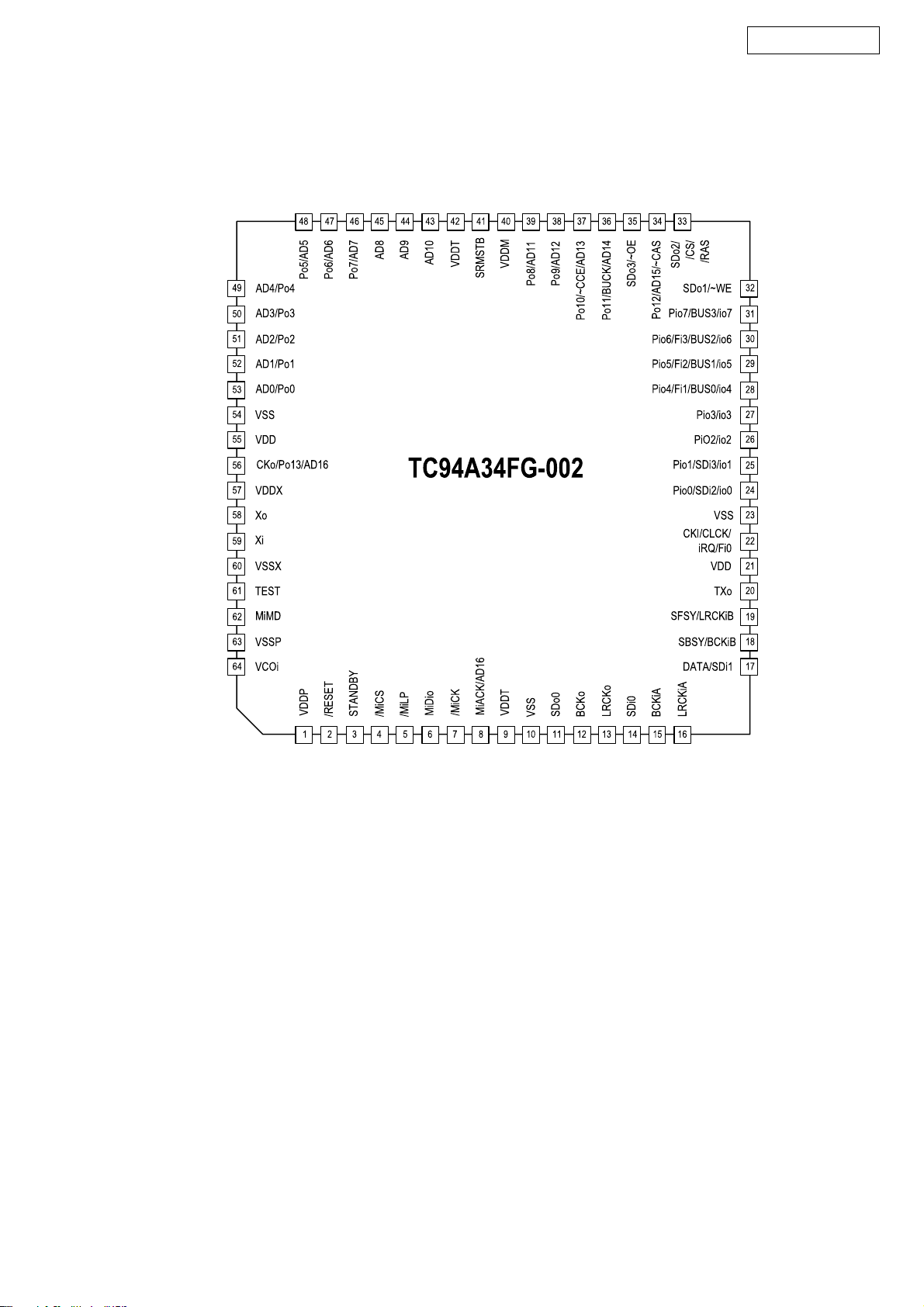
TC94A34FAG (IC306 : 1U-3760)
PIN ARRANGEMENT
S-81/S-81DAB
30
Page 31

PIN DESCRIPTIONS
S-81/S-81DAB
31
Page 32

S-81/S-81DAB
32
Page 33

S-81/S-81DAB
33
Page 34

TC94A14FAG (IC307 : 1U-3760)
R
K
A
A
K
K
K
K
A
Y
Y
S-81/S-81DAB
DV
DV
DV
DV
ZDET
V
BUS0
BUS1
BUS2
BUS3
BUC
/CCE
/RST
SS3
RO
DD3
LO
SS3
SS5
49
50
51
52
53
54
55
56
57
58
59
60
61
62
63
48
DD3
XV
LPF
XO
generator
Micro-
controller
interface
XI
Clock
SS3
XV
1-bit
DAC
Audio out
circuit
Correction
TESIN
circuit
DD3VSS3
V
Address
circuit
16 k
RAM
Digital output
DMO
FMO
PWM
Servo control
ROM
RAM
DD3
AV
Digital equalizer
adjustment circuit
CLV servo
Synchronous
guarantee
EFM
decoder
Sub code
decoder
SEL
TEBC
automatic
RFGC
A/D
VCO
PLL
TMAX
REF
V
D/A
Data
slicer
TRO
FOO
3347 46 45 44 43 42 41 40 39 38 37 36 35 34
TEZI
32
31
TEI
SBAD
30
FEI
29
28
RFRP
27
RFZI
26
RFCT
V
25
DD3
RFI
24
SLCO
23
V
22
SS3
VCOF
21
PV
20
REF
LPFO
19
LPFN
18
V
64
DD5
1 162 3 4 5 6 7 8 9 10 11 12 13 14 15
BC
LRC
AOUT
IPF
DOUT
DD3
V
SS3
V
SBO
CLC
SFS
DAT
IO0
IO1
SBS
DD3
PV
Pin Functions
Pin No. Symbol I/O Function Description Remarks
1BCK
2 LRCK
3AOUT
4 DOUT
5IPF
6V
7V
DD3
SS3
8SBOK
9CLCK
10 DA TA
O
Bit clock output pin. 32fs, 48fs, or 64fs selectable by command.
3-5I/F
O
L/R channel clock output pin. “L” for L channel and “H” for R
3-5I/F
channel. Output polarity can be inverted by command.
O
Audio data output pin. MSB-first or LSB-first selectable by
3-5I/F
command.
O
Digital data output pin. Outputs up to double-speed playback. Based on CP-1201
3-5I/F
O
Correction flag output pin. When set to “H”, AOUT output cannot
3-5I/F
be corrected by C2 correction processing.
ˇ Digital 3.3 V power supply voltage pin. ˇ
-
ˇ Digital GND pin. ˇ
-
O
Subcode Q data CRCC result output pin. “H” level when result is
3-5I/F
OK.
I/O
Subcode P-W data read clock I/O pin. I/O polarity selectable by
3-5I/F
command.
O
Subcode P-W data output pin. ˇ
3-5I/F
Normal speed:
32fs ı 1.4112 MHz
=
Normal speed: 44.1 kHz
Alias: C2PO
Schmitt input
TMAX
17
PDO
ˇ
-
-
-
-
ˇ
-
34
Page 35

Pin No. Symbol I/O Function Description Remarks
S-81/S-81DAB
11 S FSY
12 S BSY
13 I O0
14 I O1
15 P V
16 P DO
17 TMAX
18 LP FN
19 LP FO
20 PV
21 VCOF
DD3
REF
O
Playback frame sync signal output pin. ˇ
3-5I/F
O
Subcode block sync signal output pin. “H” level at S1 when
3-5I/F
subcode sync is detected.
I/O
General-purpose input / output pins.
3-5I/F
Input port at reset.
ˇ PLL-only 3.3 V power supply voltage pin. ˇ
-
O
EFM and PLCK phase difference signal output pin.
AI/F
TMAX detection result output pin.
TMAX Detection Result TMAX Output
O
AI/F
I
AI/F
O
AI/F
ˇ PLL-only V
-
O
AI/F
Longer than fixed period “PV
Within fixed period “HiZ”
Shorter than fixed period “AV
Inverted input pin for PLL LPF amp. Analog input
Output pin for PLL LPF amp. Analog output
pin. ˇ
REF
VCO filter pin. Analog output
DD3
SS3
”
”
Schmittatinput
4-state output
,HiZ,PV
(PV
DD3
3-state output
,HiZ,AV
(PV
DD3
-
ˇ
-
-
,AV
REF
SS3
)
SS3
)
-
22 AV
23 S LCO
24 RFI
25 AV
26 RFCT
27 RFZI
28 RFRP
29 FE I
30 SBAD
31 TE I
32 TE ZI
33 FOO
34 TRO
SS3
DD3
ˇ Analog GND pin. ˇ
-
O
DAC output pin for data slice level generation. Analog output
AI/F
I
RF signal input pin. Zin selectable by command. Analog input
AI/F
ˇ Analog 3.3 V power supply voltage pin. ˇ
-
I
RFRP signal center level input pin. Analog input: Zin ı 33 k
AI/F
I
RFRP signal zero-cross input pin. Analog input
AI/F
I
RF ripple signal input pin. Analog input
AI/F
I
Focus error signal input pin. Analog input
AI/F
I
Sub-beam adder signal input pin. Analog input
AI/F
I
Tracking error input pin. Inputs when tracking servo is on. Analog input
AI/F
I
Tracking error signal zero-cross input pin. Analog input: Zin ı 10 k
AI/F
O
Focus equalizer output pin.
AI/F
O
Tracking equalizer output pin.
AI/F
Analog output
~AV
(AV
SS3
-
-
DD3
=
=
)
35 V
36 RFGC
37 TE BC
REF
ˇ Analog reference power supply voltage pin. ˇ
-
O
RF amplitude adjustment control signal output pin.
AI/F
O
Tracking balance control signal output pin.
AI/F
3-state output
(PWM carrier ı 88.2 kHz)
(AV
DD3,VREF
35
-
=
,AV
SS3
)
Page 36

Pin No. Symbol I/O Function Description Remarks
O
38 S EL
39 AV
40 FMO
41 DMO
DD3
APC circuit ON/OFF signal output pin. At laser on, high
AI/F
impedance with UHS ı “L”, H output with UHS ı “H”.
-
ˇ Analog 3.3 V power supply voltage pin. ˇ
O
Feed equalizer output pin.
AI/F
O
Disc equalizer output pin.
AI/F
3-state output
3-state output
(PWM carrier ı 88.2 kHz)
(AV
DD3,VREF
-
=
,AV
S-81/S-81DAB
)
SS3
42 V
43 V
44 TE SIN
45 X V
46 X I
47 XO
48 X V
49 DV
50 RO
51 DV
52 DV R ˇ Reference voltage pin.
53 LO
54 DV
55 ZDE T
SS3
DD3
SS3
DD3
SS3
DD3
SS3
ˇ Digital GND pin.
-
ˇ Digital 3.3 V power supply voltage pin.
-
I
Test input pin. Normally, fixed to “L”.
3I/F
ˇ System clock oscillator GND pin.
-
I
System clock oscillator input pin.
AI/F
O
System clock oscillator output pin.
AI/F
-
ˇ System clock oscillator 3.3 V power supply voltage pin.
ˇ DA converter GND pin.
-
O
R-channel data forward output pin.
AI/F
ˇ DA converter 3.3 V power supply pin.
-
-
O
L-channel data forward output pin.
AI/F
-
ˇ DA converter GND pin. ˇ
O
1 bit DA converter zero data detection flag output pin. ˇ
3-5I/F
-
-
-
-
-
-
-
-
-
-
-
-
-
-
56 V
57 B US0
58 B US1
59 B US2
60 B US3
61 B UCK
62 / CCE
63 / RST
64 V
SS5
DD5
ˇ Microcontroller interface GND pin. ˇ
-
I/O
Microcontroller interface data I/O pins.
3-5I/F
I
Microcontroller interface clock input pin. Schmitt input
3-5I/F
I
Microcontroller interface chip enable signal input pin. At “L”,
3-5I/F
BUS0 to BUS3 are active.
I
Reset signal input pin. At reset, “L”. Built-in pull-up resistor
3-5I/F
ˇ Microcontroller interface 5 V power supply pin. ˇ
-
Schmitt input
CMOS ports
Schmitt input
-
-
36
Page 37

TC7WH157FU (IC308 : 1U-3760)
OUTPUT
S-81/S-81DAB
Vcc7ST
8
1
A
2
B
SELECT
6
3Y4
Y
5
GND
SN74LV244A (IC309 : 1U-3760)
(TOP VIEW)
1
1OE
1A1
2Y4
1A2
2Y3
1A3
2Y2
1A4
2Y1
GND
2
3
4
5
6
7
8
9
10
20
19
18
17
16
15
14
13
12
11
V
CC
2OE
1Y1
2A4
1Y2
2A3
1Y3
2A2
1Y4
2A1
FUNCTION TABLE
(each buffer)
INPUTS
OE A
L H H
L LL
H X Z
OUTPUT
Y
logic diagram (positive logic)
1
1OE
218
1A1
416
1A2
614
1A3
812
1A4
1Y1
1Y2
1Y3
1Y4
19
2OE
11 9
2A1
13 7
2A2
15 5
2A3
17 3
2A4
2Y1
2Y2
2Y3
2Y4
37
Page 38

S-81/S-81DAB
BU2090F (IC601 : 1U-3762)
PIN FUNCTIONS
Pin
NO.
1Vss -GND
2DATA I Serial Data
3 CLOCK I Data Shift Clock
4 Q0 O Parallel Data Bit0
5 Q1 O Parallel Data Bit1
6 Q2 O Parallel Data Bit2
7 Q3 O Parallel Data Bit3
8 Q4 O Parallel Data Bit4
9 Q5 O Parallel Data Bit5
10 Q6 O Parallel Data Bit6
11 Q7 O Parallel Data Bit7
12 Q8 O Parallel Data Bit8
13 Q9 O Parallel Data Bit9
14 Q10 O Parallel Data Bit10
15 Q11 O Parallel Data Bit11
16 VDD - Power Supply
Symbol I/O Function
PCM1803 (IC704 : 1U-3762)
L
V
IN
V
1
REF
Reference
V
2
REF
VINL
V
IN
V
REF
V
REF
V
CC
AGND
PDWN
BYPAS
TEST
LRCK
Delta-Sigma
(TOP VIEW)
1
R
1
2
2
3
4
5
6
7
8
9
10
BLOCK DIAGRAM
Modulator
20
19
18
17
16
15
14
13
12
11
x
1/64 , x1/128
Decimation
HighœPass Filter
Filter
With
MODE1
MODE0
FMT1
FMT0
OSR
SCKI
V
DD
DGND
DOUT
BCK
Serial
Interface
Mode/
Format
Control
BCK
LRCK
DOUT
FMT0
FMT1
V
R
IN
Power Supply
AGNDV
CC
Delta-Sigma
Modulator
DGND
Clock and T iming Control
V
DD
MODE0
MODE1
BYPAS
TEST
OSR
PDWN
SCKI
38
Page 39

S-81/S-81DAB
SELECT
Y
TERMINAL
NAME NO.
I/O DESCRIPTION
AGND 6 – Analog GND
BCK 11 I/O Audio data bit clock input/output
(1)
BYPAS 8 I HPF bypass control. LOW: Normal mode (dc reject); HIGH: Bypass mode (through)
DGND 13 – Digital GND
DOUT 12 O Audio data digital output
FMT0 17 I Audio data format select input 0. See Data Format section.
FMT1 18 I Audio data format select input 1. See Data Format section.
LRCK 10 I/O Audio data latch enable input/output
MODE0 19 I Mode select input 0. See Data Format section.
MODE1 20 I Mode select input 1. See Data Format section.
(1)
(2)
(2)
OSR 16 I Oversampling ratio select input. LOW: ´ 64 fS, HIGH: ´ 128 f
PDWN 7 I Power-down control, active-low
SCKI 15 I System clock input: 256 fS, 384 fS, 512 fSor 768 f
TEST 9 I Test, must be connected to DGND
V
CC
V
DD
V
L 1 I Analog input, L-channel
IN
V
R 2 I Analog input, R-channel
IN
1 3 – Reference-voltage-1 decoupling capacitor
V
REF
2 4 – Reference-voltage-2 decoupling capacitor
V
REF
5 – Analog power supply, 5-V
14 – Digital power supply, 3.3-V
(2)
S
(2)
(2)
(2)
(2)
S
(3)
(1) Schmitt-trigger input
(2) Schmitt-trigger input with internal pulldown (50 kW typically), 5-V tolerant
(3) Schmitt-trigger input, 5-V tolerant
(2)
SN74LV157A (IC705,706 : 1U-3762)
(TOP VIEW)
A/B
1
1A
2
1B
3
1Y
4
5
2A
6
2B
7
2Y
G
8
SELECT
GND
H X X X L
L L L XL
L L H XH
L H X LL
L H X H H
V
16
CC
G
15
4A
14
4B
13
12
4Y
11
3A
10
3B
9
3Y
FUNCTION TABLE
INPUTS
DATA
A/B
A B
logic diagram (positive logic)
OUTPUT
A/B
2
1A
4
3
1B
5
2A
6
2B
11
3A
10
3B
14
4A
13
4B
15
G
1
1Y
7
2Y
9
3Y
12
4Y
Pin numbers shown are for the D, DB, DGV, J, NS, PW, and W packages.
39
Page 40

TAS5504PAG(IC707 : 1U-3762)
S-81/S-81DAB
40
Page 41

S-81/S-81DAB
41
Page 42

S-81/S-81DAB
42
Page 43

TAS5142DKD (IC709 : 1U-3762)
S-81/S-81DAB
DKD PACKAGE
(TOP VIEW)
RESET_AB
RESET_CD
Terminal Functions
TERMINAL
NAME DKD NO.
GVDD_B 1
OTW
SD
PWM_A 4
RESET_AB
PWM_B 6
OC_ADJ 7
GND 8
AGND 9
VREG 10
M3 11
M2 12
M1 13
PWM_C 14
RESET_CD 15
PWM_D 16
VDD 17
GVDD_C 18
GVDD_D 19
BST_D 20
PVDD_D 21
OUT_D 22
GND_D 23
GND_C 24
OUT_C 25
PVDD_C 26
BST_C 27
BST_B 28
PVDD_B 29
OUT_B 30
GND_B 31
GND_A 32
OUT_A 33
PVDD_A 34
BST_A 35
GVDD_A 36
(1) power
I = input, O = output, P =
2
3
5
GVDD_B
OTW
SD
PWM_A
PWM_B
OC_ADJ
GND
AGND
VREG
M3
M2
M1
PWM_C
PWM_D
VDD
GVDD_C
FUNCTION
1
2
3
4
5
6
7
8
9
10
11
12
13
14
15
16
17
18
(1)
GVDD_A
36
BST_A
35
34
PVDD_A
OUT_A
33
32
GND_A
GND_B
31
30
OUT_B
29
PVDD_B
28
BST_B
27
BST_C
26
PVDD_C
25
OUT_C
24
GND_C
23
GND_D
22
OUT_D
21
PVDD_D
20
BST_D
19
GVDD_D
DESCRIPTION
P Gate-drive voltage supply requires 0.1-µF capacitor to AGND
O Overtemperature warning signal, open-drain, active-low
O Shutdown signal, open-drain, active-low
I Input signal for half-bridge A
I Reset signal for half-bridge A and half-bridge B, active-low
I Input signal for half-bridge B
O Analog overcurrent programming pin requires resistor to ground
P Ground
P Analog ground
P Digital regulator supply filter pin requires 0.1-µF capacitor to AGND.
I Mode selection pin
I Mode selection pin
I Mode selection pin
I Input signal for half-bridge C
I Reset signal for half-bridge C and half-bridge D, active-low
I Input signal for half-bridge D
P Power supply for digital voltage regulator requires 0.1-µF capacitor
to GND.
P Gate-drive voltage supply requires 0.1-µF capacitor to AGND
P Gate-drive voltage supply requires 0.1-µF capacitor to AGND
P HS bootstrap supply (BST), external capacitor to OUT_D required
P Power supply input for half-bridge D requires close decoupling of
0.1-µF capacitor to GND_D.
O Output, half-bridge D
P Power ground for half-bridge D
P Power ground for half-bridge C
O Output, half-bridge C
P Power supply input for half-bridge C requires close decoupling of
0.1-µF capacitor to GND_C.
P HS bootstrap supply (BST), external capacitor to OUT_C required
P HS bootstrap supply (BST), external capacitor to OUT_B required
P Power supply input for half-bridge B requires close decoupling of
0.1-µF capacitor to GND_B.
O Output, half-bridge B
P Power ground for half-bridge B
P Power ground for half-bridge A
O Output, half-bridge A
P Power supply input for half-bridge A requires close decoupling of
0.1-µF capacitor to GND_A.
P HS bootstrap supply (BST), external capacitor to OUT_A required
P Gate-drive voltage supply requires 0.1-µF capacitor to AGND
43
Page 44

STR-F6238S (IC902 : 1U-3762)
S-81/S-81DAB
44
Page 45

SPI-8002TW (IC901 : 1U-3762)
S-81/S-81DAB
14
AGND
V
V
SW
OUT1
DGND1
SS1
V
REF1
NC
C/E
1
IN1
CC
SK
16
NC
V
C/E
SW
IN2
OUT2
DGND2
SS2
V
REF2
8
3
V
CC
SPI-8001TW/SPI-8002TW
AGND
9
3V
V
REF
PRegStart
OSC
RESET
RESET
TSDfdown
UVLO
1V
IN1
V
2
fdown
cut
3V
OCP
SS16
Amp
3V
+
Ð
Ð
PWM
7
V
REF1
+
Ð
+
Ð
Buffer-Amp
fdown
cut
AGND
SS211
10
V
REF2
AGND
+
Ð
Buffer-Amp
+
Ð
Amp
+
Ð
Ð
PWM
AGND
PWM
Logic
PWM
Logic
Drive
Drive
OCP
SW
OUT1
DGND1
V
SW
OUT2
DGND2
4
5
15
IN2
13
12
45
Page 46

PCM1754 (IC103 : 1U-3790)
S-81/S-81DAB
BCK
DATA
LRCK
DGND
NC
V
V
OUT
V
OUT
(TOP VIEW)
16
15
14
13
12
11
10
9
CC
1
2
3
4
5
6
L
7
R
8
FUNCTIONAL BLOCK DIAGRAM
SCK
FMT
MUTE
DEMP
TEST
ZEROA
V
COM
AGND
Terminal Functions
TERMINAL
NAME NO.
AGND 9–Analog ground
BCK 1 I Audio-data bit-clock input
DATA 2 I Audio-data digital input
DEMP 13 I De-emphasis control
DGND 4 – Digital ground
FMT 15 I Data format select
LRCK 3 I L-channel and R-channel audio data latch enable input
MUTE 14 I Analog mixing control
NC 5 –
SCK 16 I System clock input
TEST 12 I Test pin. Ground or open
V
CC
V
COM
V
L 7 O Analog output for L-channel
OUT
V
R 8 O Analog output for R-channel
OUT
ZEROA 11 O Zero flag output for L/R channels
(1)
Schmitt-trigger input with internal pulldown.
I/O
6 – Analog power supply, 5 V
10 – Common voltage decoupling
DESCRIPTION
(1)
(1)
(1)
(1)
BCK
LRCK
DATA
FMT
MUTE
DEMP
TEST
SCK
Audio
Serial
Port
Serial
Control
Port
System
Clock
Manager
Oversampling
Function
Control
System Clock
4x/8x
Digital
Filter
and
Zero Detect
Enhanced
Multilevel
Delta-Sigma
Modulator
ZEROA
DAC
DAC
Power Supply
CC
V
DGND
Output Amp
and
Low-Pass Filter
Output Amp
and
Low-Pass Filter
AGND
V
V
V
OUT
COM
OUT
L
R
46
Page 47

BD3812F (IC202 : 1U-3790)
S-81/S-81DAB
IN1
AGND1
IN2
AGND2
V
AGND3
V
1
EE
CC
7
14
OUT1
OUT2
SEL
DGND
MUTE
DA
CL
8
F2602 (IC102 : 1U-3790)
47
Page 48

S-81/S-81DAB
48
Page 49

S-81/S-81DAB
49
Page 50

2. FL DISPLAY
16-ST-88GINK (FL 601)
1 43
S-81/S-81DAB
Grid Assignment
16G 15G 14G 13G 12G 11G 10G 9G 8G 7G 6G 5G 4G 3G 2G 1G
( Upper display) ( Lower display)
1-1A 2-1A 3-1A 4-1A 5-1A
-
2A 2-2A 3-2A 4-2A 5-2A
1
-
3A 2-3A 3-3A 4-3A 5-3A
1
-
4A 2-4A 3-4A 4-4A 5-4A
1
1
-
5A 2-5A 3-5A 4-5A 5-5A
1-1B 2-1B 3-1B 4-1B 5-1B
-
2B 2-2B 3-2B 4-2B 5-2B
1
-
3B 2-3B 3-3B 4-3B 5-3B
1
-
4B 2-4B 3-4B 4-4B 5-4B
1
1
-
5B 2-5B 3-5B 4-5B 5-5B
-
6A 2-6A 3-6A 4-6A 5-6A
1
1
-
7A 2-7A 3-7A 4-7A 5-7A
[ 16G~1G ]
50
-
6B 2-6B 3-6B 4-6B 5-6B
1
1
-
7B 2-7B 3-7B 4-7B 5-7B
Page 51

Pin Connection
CONNECTION
NOTE 1) F1, F2 : Filament
10) CP : Shift Register Clock
11) DA : Serial Data Input
12) TSA, B : Test pin
13) CS : Chip Select Input pin
14) RESET : Reset Input
15) OSC : Pin for self-oscillation
PIN NO.
2) NP : No pin
3) NC : No connection
(NC pin should be electrically open on the PC board)
4) NX : No extend pin
5) DL : Datum Line
6) LGND : Logic GND pin
7) PGND : Power GND pin
8) VH : High Voltage Supply pin
9) VDD : Logic Voltage Supply pin
3
2
1
N
N
F
P
P
1
151
4
~
4
~
N
N
C
X
2
3
1
0
9
T
S
B
4
-
T
D
C
C
S
A
P
S
A
3
3
3
3
3
2
S-81/S-81DAB
4
4
4
3
4
3
3
3
3
8
6
7
5
R
E
O
S
V
S
E
V
D
C
T
H
D
2
1
0
9
P
G
N
D
3
L
G
N
N
N
F
P
P
D
2
51
Page 52

PRINTED WIRING BOARDS
00D 1U-3760 CD P.W.B. UNIT
S-81/S-81DAB
52
COMPONENT SIDE
2
Page 53

S-81/S-81DAB
53
FOIL SIDE
2
Page 54

00D 1U-3761 SUCOM/SELECTOR P.W.B. UNIT
S-81/S-81DAB
54
COMPONENT SIDE
2
Page 55

S-81/S-81DAB
55
FOIL SIDE
2
Page 56

00D 1U-3762 SMPS/D.AMP P.W.B. UNIT
S-81/S-81DAB
56
COMPONENT SIDE
2
Page 57

S-81/S-81DAB
57
FOIL SIDE
2
Page 58

00D 1U-3769 DAB CONNECT P.W.B. UNIT
S-81/S-81DAB
COMPONENT SIDE
FOIL SIDE
58
Page 59

00D 1U-3790 MONO OUT P.W.B. UNIT
S-81/S-81DAB
COMPONENT SIDE
2
59
FOIL SIDE
2
Page 60

S-81/S-81DAB
NOTE FOR PARTS LIST
• Part indicated with the mark "nsp" are not always in stock and possibly to
take a long period of time for supplying, or in some case supplying of part
may be refused.
• When ordering of part, clearly indicate "1" and "I" (i) to avoid mis-
supplying.
• Ordering part without stating its part number can not be supplied.
• Part indicated with the mark " ★ " is not illustrated in the exploded view.
• Not including General-purpose Carbon Film Resistor in the P.W.Board
parts list. (Refer to the Schematic Diagram for those parts.)
• Not including General-purpose Carbon Chip Resistor in the P.W.Board
parts list. (Refer to the Schematic Diagram for those parts.)
WARNING:
Parts marked with this symbol ! have critical characteristics.
Use ONLY replacement parts recommended by the manufacturer.
ll
Resistors
l
ll
Ex.: RN 14K 2E 182 G FR
Type Shape Power Resist- Allowable Others
and per- ance error
formance
RD : Carbon 2B : 1/8W F : ±1% P : Pulse-resistant type
RC : Composition 2E : 1/4W G : ±2% NL : Low noise type
RS : Metal oxide film 2H : 1/2W J : ±5% NB : Non-burning type
RW : Winding 3A : 1W K : ±10% FR : Fuse-resistor
RN : Metal film 3D : 2W M : ±20% F : Lead wire forming
RK : Metal mixture 3F : 3W
] Resistance
1 8 2 ⇒ 1800 ohm = 1.8 kohm
s
s
• Units: ohm
1 R 2 ⇒ 1.2 ohm
s
s
• Units: ohm
3H : 5W
Indicates number of zeros after effective number.
2-digit effective number.
1-digit effective number.
2-digit effective number, decimal point indicated by R.
部品表について
1.nsp 印の部品は常時在庫していませんので供給に長時間を要すること
があります。
場合によっては、供給をお断りすることがあります。
2.部品を発注する際は特に数字の " 1 " と英字の "I" との区別をはっき
り記入してください。
3.部品番号を表示していない部品は供給できません。
4.!印の部品は安全上重要な部品です。交換するときは、安全および性
能維持のため必ず指定の部品をご使用ください。
5.★印のついている部品は分解図中には記載していません。
6.汎用カーボン抵抗器は記載していません。定数は回路図を参照願いま
す。
7.汎用カーボンチップ抵抗器は記載していません。定数は回路図を参照
願います。
8.部品表の抵抗器、コンデンサの品名記号の読み方は表を参照してくだ
さい。
RN 14K 2E 182 G FR
RD : 2B : 1/8 W F : ±1% P :
RC : 2E : 1/4 W G : ±2% NL :
RS : 2H : 1/2 W J : ±5% NB :
RW : 3A : 1 W K : ±10% FR :
RN : 3D : 2 W M : ±20% F :
RK : 3F : 3 W
∗
18 2
1R 2
3H : 5 W
1800
Ö
2
1.2
Ö
1
2 R
=1.8k
0
ll
l Capacitors
ll
Ex.: CE 04W 1H 2R2 M BP
Type Shape Dielectric Capacity Allowable Others
and per- strength error
formance
CE : Aluminum foil 0J : 6.3V F : ±1% HS : High stability type
electrolytic
CA : Aluminum solid 1A : 10V G : ±2% BP : Non-polar type
electrolytic
CS : Tantalum electrolytic 1C : 16V J : ±5% HR : Ripple-resistant type
CQ : Film 1E : 25V K : ±10% DL : For change and discharge
CK : Ceramic 1V : 35V M : ±20% HF : For assuring high
CC : Ceramic 1H : 50V Z : +80% U : UL par t
CP : Oil 2A : 100V –20% C : CSA part
CM : Mica 2B : 125V P : +100% W : UL-CSA type
CF : Metallized 2C : 160V –0% F : Lead wire forming
CH : Metallized 2D : 200V C : ±0.25pF
] Capacity (electrolyte only)
2 2 2 ⇒ 2200µF
s
s
• Units: µF.
2 R 2 ⇒ 2.2µF
s
s
• Units: µF.
] Capacity (except electrolyte)
2 2 2 ⇒ 2200pF=0.0022µF
s
s
(More than 2) Indicates number of zeros after effective number.
• Units: pF.
2 2 1 ⇒ 220pF
s
s
(0 or 1) Indicates number of zeros after effective number.
• Units: pF.
• When the dielectric strength is indicated in AC, "AC" is included after the dieelectric
strength value.
2E : 250V D : ±0.5pF
2H : 500V = : Others
2J : 630V
Indicates number of zeros after effective number.
2-digit effective number.
1-digit effective number.
2-digit effective number, decimal point indicated by R.
2-digit effective number.
2-digit effective number.
requency
CE 04W 1H 2R2 M BP
CE : 0J : 6.3 V F : ±1% HS :
CA : 1A : 10 V G : ±2% BP :
CS : 1C : 16 V J : ±5% HR :
CQ : 1E : 25 V K : ±10% DL :
CK : 1V : 35 V M : ±20% HF :
CC : 1H : 50 V Z : +80% U : UL
CP : 2A : 100 V −20% C : CSA
CM : 2B : 125 V P : +100% W : UL-CSA
CF : 2C : 160 V − 0% F :
CH : 2D : 200 V C : ±0.25pF
2E : 250 V D : ±0.5pF
2H : 500 V = :
2J : 630 V
∗
22 2
22 2
2200µF
Ö
2
µ
F
2200pF=0.0022µF
Ö
(0 2 )
2
p
F
0
0
2R 2
22 1
Ö
1
2 R
µ
F
Ö
(0 0 1 )
2
p
F
AC
2.2µF
220pF
0
60
Page 61

S-81/S-81DAB
PARTS LIST OF P.W.B. UNIT
*本表に記載されている部品は、補修用部品のため製品に使用している部品とは一部、形状、寸法などが異なる場合があります。
* The parts listed below are for maintenance only, might differ from the parts used in the unit in appearances or dimensions.
*"nsp" 印の部品は常時在庫していませんので供給に長時間を要することがあります。場合によっては、供給をお断りする場合があります。
* Part indicated with the mark “nsp” are not always in stock and possibly to take a long period of time for supplying, or in some case supplying of part may be refused.
Note: The symbols in the column "Remarks" indicate the following destinations.
E3 : U.S.A. & Canada model EK : U.K. model with DAB
E2 : Europe model JP : Japan model
00D1U-3760 CD P.W.B. UNIT ASS'Y
Ref. No. nsp Part No. Part Name Remarks Q'ty New
SEMICONDUCTORS GROUP
IC301 00D 263 0994 908 BA6287F-E2 +C
IC302 00D GEN 8165 CD ROM ASSY TMP91FY42FG *
IC303 00D 263 1191 904 TA2157FNG
IC304 00D 263 1220 901 TA2125AFG
IC306 00D 262 3596 009 TC94A34FG-002
IC307 00D 262 3255 007 TC94A14FAG
IC308 00D 262 3046 902 TC7WH157FU +C
IC309 00D 262 2959 906 SN74LV244APW +REF
IC315 00D 263 1248 909 UPD120N15T1B-E1-AZ
TR301 00D 272 0125 904 2SB709A +C
TR302 00D 269 0082 902 DTC114EKT96 +C
D301-303 00D 276 0717 903 1SS355 TE-17 +C
ZD301 00D 276 0798 951 UDZS4.7B-TE17
RESISTORS GROUP
R451 00D 235 0130 903 CHIP EMIFIL(11A121) +1608
R323 00D 244 2052 928 RS14B3A470JNBST(S)
CAPACITORS GROUP
C301 nsp 00D 257 0509 929 CK73B1H102KT +1608
C302 nsp 00D 257 0501 901 CK73B1H103KT (1608) +1608
C303 nsp 00D 257 0516 954 CK73B1E104KT +1608
C304 nsp 00D 257 0501 901 CK73B1H103KT (1608) +1608
C305 nsp 00D 257 0509 929 CK73B1H102KT +1608
C306 00D 254 4738 904 CE67W0J101MT(GV)
C307 nsp 00D 257 0516 954 CK73B1E104KT +1608
C308 nsp 00D 257 0501 901 CK73B1H103KT (1608) +1608
C309 nsp 00D 257 0509 929 CK73B1H102KT +1608
C310,311 nsp 00D 257 0516 954 CK73B1E104KT +1608
C312 nsp 00D 257 0501 901 CK73B1H103KT (1608) +1608
C313 nsp 00D 257 0509 929 CK73B1H102KT +1608
C317-320 nsp 00D 257 0516 954 CK73B1E104KT +1608
C321 nsp 00D 257 0501 901 CK73B1H103KT (1608) +1608
C322,323 nsp 00D 257 0516 954 CK73B1E104KT +1608
C324 nsp 00D 257 0501 901 CK73B1H103KT (1608) +1608
C329 00D 254 4740 934 CE67W1C101MT(GV)
C330 nsp 00D 257 0516 954 CK73B1E104KT +1608
C331 nsp 00D 257 0501 901 CK73B1H103KT (1608) +1608
C332 00D 254 4738 904 CE67W0J101MT(GV)
C333 nsp 00D 257 0516 954 CK73B1E104KT +1608
61
Page 62

S-81/S-81DAB
Ref. No. nsp Part No. Part Name Remarks Q'ty New
C340 nsp 00D 257 0516 954 CK73B1E104KT +1608
C343,344 nsp 00D 257 0516 954 CK73B1E104KT +1608
C345 00D 254 4738 904 CE67W0J101MT(GV)
C346 nsp 00D 257 0516 954 CK73B1E104KT +1608
C347 nsp 00D 257 0501 901 CK73B1H103KT (1608) +1608
C348 nsp 00D 257 0516 954 CK73B1E104KT +1608
C349 nsp 00D 257 0516 909 CK73B1E223KT +1608
C350 nsp 00D 257 0510 905 CK73B1H272KT +1608
C351 00D 254 4740 934 CE67W1C101MT(GV)
C352 00D 254 4738 904 CE67W0J101MT(GV)
C353-355 nsp 00D 257 0516 954 CK73B1E104KT +1608
C356-358 nsp 00D 257 0509 929 CK73B1H102KT +1608
C359 00D 254 4740 934 CE67W1C101MT(GV)
C360,361 nsp 00D 257 0516 954 CK73B1E104KT +1608
C366 nsp 00D 257 0516 954 CK73B1E104KT +1608
C367 nsp 00D 257 0501 901 CK73B1H103KT (1608) +1608
C368 nsp 00D 257 0502 942 CC73CH1H2R0CT +1608
C369 nsp 00D 257 0516 954 CK73B1E104KT +1608
C370 00D 254 4740 934 CE67W1C101MT(GV)
C371 00D 254 4738 904 CE67W0J101MT(GV)
C373 nsp 00D 257 0505 907 CC73CH1H560JT +1608
C374,375 nsp 00D 257 0516 954 CK73B1E104KT +1608
C376 00D 254 4738 904 CE67W0J101MT(GV)
C377 nsp 00D 257 0516 954 CK73B1E104KT +1608
C378 00D 254 4738 904 CE67W0J101MT(GV)
C379 nsp 00D 257 0501 901 CK73B1H103KT (1608) +1608
C380 nsp 00D 257 0516 909 CK73B1E223KT +1608
C381,382 00D 254 4738 904 CE67W0J101MT(GV)
C383,384 nsp 00D 257 0501 901 CK73B1H103KT (1608) +1608
C385 nsp 00D 257 0516 954 CK73B1E104KT +1608
C386 00D 254 4738 904 CE67W0J101MT(GV)
C387-389 nsp 00D 257 0516 954 CK73B1E104KT +1608
C390 nsp 00D 257 0509 929 CK73B1H102KT +1608
C391 nsp 00D 257 0509 990 CK73B1H222KT +1608
C392-394 nsp 00D 257 0516 954 CK73B1E104KT +1608
C395 nsp 00D 257 0508 917 CC73CH1H471JT +1608
C396,397 nsp 00D 257 0501 901 CK73B1H103KT (1608) +1608
C398 00D 254 4738 904 CE67W0J101MT(GV)
C399 nsp 00D 257 0516 941 CK73B1E473KT +1608
C400 nsp 00D 257 0508 917 CC73CH1H471JT +1608
C401 nsp 00D 257 0516 954 CK73B1E104KT +1608
C402 nsp 00D 257 0504 982 CC73CH1H470JT +1608
C403 nsp 00D 257 0501 927 CK73B1H153KT +1608
C404,405 nsp 00D 257 0516 941 CK73B1E473KT +1608
C406 nsp 00D 257 0516 925 CK73B1E333KT +1608
C407 nsp 00D 257 0516 954 CK73B1E104KT +1608
C408 00D 257 3006 924 CF73=1C103JT(ECHUB5)+2125
C409 nsp 00D 257 0501 901 CK73B1H103KT (1608) +1608
C410 nsp 00D 257 0509 990 CK73B1H222KT +1608
C411 nsp 00D 257 0516 925 CK73B1E333KT +1608
C412 nsp 00D 257 0516 941 CK73B1E473KT +1608
C413 nsp 00D 257 0516 954 CK73B1E104KT +1608
C414 00D 254 4738 904 CE67W0J101MT(GV)
C415 nsp 00D 257 0516 954 CK73B1E104KT +1608
C416 00D 254 4738 904 CE67W0J101MT(GV)
C417 nsp 00D 257 0516 954 CK73B1E104KT +1608
62
Page 63

S-81/S-81DAB
Ref. No. nsp Part No. Part Name Remarks Q'ty New
C418 nsp 00D 257 0516 909 CK73B1E223KT +1608
C419 nsp 00D 257 0516 941 CK73B1E473KT +1608
C420 nsp 00D 257 0516 954 CK73B1E104KT +1608
C421 nsp 00D 257 0501 901 CK73B1H103KT (1608) +1608
C422 nsp 00D 257 0516 954 CK73B1E104KT +1608
C423 00D 254 4738 904 CE67W0J101MT(GV)
C424 nsp 00D 257 0516 909 CK73B1E223KT +1608
C426 00D 254 4738 904 CE67W0J101MT(GV)
C427 nsp 00D 257 0516 954 CK73B1E104KT +1608
C428 00D 254 4738 904 CE67W0J101MT(GV)
C430 nsp 00D 257 0501 901 CK73B1H103KT (1608) +1608
C431 nsp 00D 257 0516 954 CK73B1E104KT +1608
C432 00D 254 4739 903 CE67W1A220MT(GV)
C433 nsp 00D 257 0501 901 CK73B1H103KT (1608) +1608
C434 nsp 00D 257 0516 909 CK73B1E223KT +1608
C435 nsp 00D 257 0501 901 CK73B1H103KT (1608) +1608
C436 nsp 00D 257 0516 954 CK73B1E104KT +1608
C437 00D 254 4738 904 CE67W0J101MT(GV)
C438 nsp 00D 257 0516 909 CK73B1E223KT +1608
C439 00D 254 4738 904 CE67W0J101MT(GV)
C440 nsp 00D 257 0516 954 CK73B1E104KT +1608
C441 nsp 00D 257 0501 901 CK73B1H103KT (1608) +1608
C442 00D 254 4738 904 CE67W0J101MT(GV)
C443 nsp 00D 257 0516 954 CK73B1E104KT +1608
C445 nsp 00D 257 0501 901 CK73B1H103KT (1608) +1608
C446,447 nsp 00D 257 0503 967 CC73CH1H150JT +1608
C448 nsp 00D 257 0516 954 CK73B1E104KT +1608
C449 nsp 00D 257 0501 901 CK73B1H103KT (1608) +1608
C450,451 nsp 00D 257 0516 954 CK73B1E104KT +1608
C452,453 nsp 00D 257 0501 901 CK73B1H103KT (1608) +1608
C454 nsp 00D 257 0509 929 CK73B1H102KT +1608
C455 nsp 00D 257 0516 954 CK73B1E104KT +1608
C456 nsp 00D 257 0501 901 CK73B1H103KT (1608) +1608
C457,458 nsp 00D 257 0516 954 CK73B1E104KT +1608
C459,460 nsp 00D 257 0501 901 CK73B1H103KT (1608) +1608
C461 nsp 00D 257 0509 929 CK73B1H102KT +1608
C462 nsp 00D 257 0516 954 CK73B1E104KT +1608
C463 nsp 00D 257 0501 901 CK73B1H103KT (1608) +1608
C464 nsp 00D 257 0516 954 CK73B1E104KT +1608
C465 nsp 00D 257 0501 901 CK73B1H103KT (1608) +1608
C466 nsp 00D 257 0509 929 CK73B1H102KT +1608
C467 nsp 00D 257 0516 954 CK73B1E104KT +1608
C468,469 00D 254 4738 904 CE67W0J101MT(GV)
C470 00D 254 4740 934 CE67W1C101MT(GV)
C471 nsp 00D 257 0516 954 CK73B1E104KT +1608
C472,473 nsp 00D 257 0501 901 CK73B1H103KT (1608) +1608
C474-477 nsp 00D 257 0516 954 CK73B1E104KT +1608
C478 00D 254 4738 904 CE67W0J101MT(GV)
C479 nsp 00D 257 0501 901 CK73B1H103KT (1608) +1608
C480 nsp 00D 257 0516 954 CK73B1E104KT +1608
C481 nsp 00D 257 0501 901 CK73B1H103KT (1608) +1608
C482 nsp 00D 257 0516 954 CK73B1E104KT +1608
C483 nsp 00D 257 0501 901 CK73B1H103KT (1608) +1608
C484 00D 254 4738 904 CE67W0J101MT(GV)
C485,486 nsp 00D 257 0516 954 CK73B1E104KT +1608
C487 nsp 00D 257 0501 901 CK73B1H103KT (1608) +1608
63
Page 64

S-81/S-81DAB
Ref. No. nsp Part No. Part Name Remarks Q'ty New
C488 nsp 00D 257 0516 954 CK73B1E104KT +1608
C489,490 nsp 00D 257 0501 901 CK73B1H103KT (1608) +1608
C491 nsp 00D 257 0516 954 CK73B1E104KT +1608
C492,493 nsp 00D 257 0509 929 CK73B1H102KT +1608
C494 nsp 00D 257 0501 901 CK73B1H103KT (1608) +1608
C495 nsp 00D 257 0516 954 CK73B1E104KT +1608
C496 nsp 00D 257 0509 929 CK73B1H102KT +1608
C498 nsp 00D 257 0501 901 CK73B1H103KT (1608) +1608
C499 nsp 00D 257 0516 954 CK73B1E104KT +1608
C500 nsp 00D 257 0509 929 CK73B1H102KT +1608
C501 nsp 00D 257 0516 954 CK73B1E104KT +1608
C502 nsp 00D 257 0501 901 CK73B1H103KT (1608) +1608
C503 nsp 00D 257 0509 929 CK73B1H102KT +1608
C504 nsp 00D 257 0501 901 CK73B1H103KT (1608) +1608
C505 nsp 00D 257 0516 954 CK73B1E104KT +1608
C506-508 nsp 00D 257 0501 901 CK73B1H103KT (1608) +1608
C509 nsp 00D 257 0516 954 CK73B1E104KT +1608
C510 nsp 00D 257 0509 929 CK73B1H102KT +1608
OTHERS PARTS GROUP
CW031 nsp 00D 203 5381 019 3P PH-SAN SHIELDCORD to CY031(3761-1) *
CW064 nsp 00D 204 0602 000 6P PH-SAN SHIELDCORD to CY064(3762-3) *
CW071 nsp 00D 204 2932 011 7P PH-SAN CON.CORD to CY071(3761-1)
CX052 nsp 00D 205 0863 952 5P PH CON.BASE(L) +REF
CX062 nsp 00D 205 0863 994 6P PH CON.BASE(L) +REF
CX063 nsp 00D 205 1072 946 6P PH CON.BASE +REF
CX161 00D 205 1314 963 16P FFC BASE(9616S)
CX171 00D 205 1343 989 17P FFC BASE(9610SC) for E2, EK
CX291 00D 205 1313 922 29P FFC.BASE(9610SCA +REF for E3, JP
FB302-307 00D 235 0130 903 CHIP EMIFIL(11A121) +1608
FB309-312 00D 235 0130 903 CHIP EMIFIL(11A121) +1608
L301 00D 235 0194 907 LB3218T101K
ST301 - STYLE PIN
ST303 - STYLE PIN
X301 00D 399 1003 906 CSTCW27M0X51-R0
X302 00D 399 1051 903 X-TAL(16.9344/HC-49)
64
Page 65

S-81/S-81DAB
00D1U-3761 SUCOM/SELECTOR P.W.B. UNIT ASS'Y
Ref. No. nsp Part No. Part Name Remarks Q'ty New
SEMICONDUCTORS GROUP
IC101 00D 262 2669 908 SN74LV157APW +C
IC102 00D 262 3360 905 LC72722PM-TLM
IC103 00D GEN 8286 MAIN ROM ASSY M3062LFGPGP / for E3 *
IC103 00D GEN 8166 MAIN ROM ASSY
IC104 235 010 0075 07S BD4727G 2.7V RESET IC
IC105 00D 262 3498 903 BR93L86RFVM-WTR
IC106 00D 262 3046 902 TC7WH157FU +C
IC107 00D 262 2517 908 SN74LV08APW-EL2 +REF
IC108 00D 269 0230 000 GP1FAV31TK0F
IC109 00D 263 0896 909 NJM2068MD-TE1 +C
IC110 00D 268 0074 904 ICP-N20T
IC201 00D 262 3166 905 PCM1748E(TAPE) +C for E3, JP
IC202 00D 263 1250 900 BD3843FS *
IC203 00D 263 0683 002 NJM7906FA
IC204 00D 263 0793 002 NJM7806FA(S)
IC205 00D 263 1221 007 BA80BC0T
IC206 00D 263 1253 017 UPC2905BHF *
IC207 00D 263 1253 004 UPC2933BHF *
IC208 00D 262 2977 946 BA33BC0FP-E2 +REF
IC209 00D 263 0615 902 BA15218F-DXE2 +C
IC210 00D 263 0615 902 BA15218F-DXE2 +C for E3, JP, EK
IC211,212 00D 263 0615 902 BA15218F-DXE2 +C
M3062LFGPGP / for JP, E2, EK
*
TR101 00D 271 0325 002 KTA1242L (O/Y)
TR102 00D 269 0192 902 KRC102S-RTK(10K-10K) +C
TR103 00D 269 0184 907 KRA102S-RTK +C
TR104 00D 269 0192 902 KRC102S-RTK(10K-10K) +C
TR105 00D 273 0464 901 KTC3875SGR-RTK +C for E3, E2, EK
TR106 00D 269 0192 902 KRC102S-RTK(10K-10K) +C
TR107,108 00D 273 0486 905 KRC231S-RTK(2.2K)
TR109 00D 269 0184 907 KRA102S-RTK +C
TR110 00D 269 0192 902 KRC102S-RTK(10K-10K) +C
TR111 00D 269 0184 907 KRA102S-RTK +C
TR112 00D 271 0324 906 KRA103S-RTK(22K-22K)
TR113 00D 269 0192 902 KRC102S-RTK(10K-10K) +C
TR201 00D 273 0303 910 2SC1740S(S)-T
TR202,203 00D 273 0384 900 2SC2412KT96(S) +C
TR204 00D 271 0324 906 KRA103S-RTK(22K-22K) for E3, JP
TR205 00D 269 0192 902 KRC102S-RTK(10K-10K) +C for E3, JP
TR207,208 00D 273 0460 905 KTC2875B-RTK +C for JP
TR209 00D 273 0464 901 KTC3875SGR-RTK +C
TR210,211 00D 273 0460 905 KTC2875B-RTK +C for JP
TR301,302 00D 269 0192 902 KRC102S-RTK(10K-10K) +C
TR651,652 00D 275 0100 902 2SK771-5-TB
TR653 00D 273 0485 906 KRC107S-RTK(10K-47K)
TR654 00D 271 0183 914 2SA933 (S)T-70
TR655 00D 269 0192 902 KRC102S-RTK(10K-10K) +C
TR656 00D 272 0150 908 2SB1243TV2(R)
D101 00D 276 0560 901 DAN202KT146 +C
D102-104 00D 276 0717 903 1SS355 TE-17 +C
D105,106 00D 276 0824 906 SFPB-64V
D201,202 00D 276 0375 905 1N4148T77 (TAPE)
D205,206 00D 276 0375 905 1N4148T77 (TAPE)
65
Page 66

S-81/S-81DAB
Ref. No. nsp Part No. Part Name Remarks Q'ty New
D217,218 00D 276 0717 903 1SS355 TE-17 +C
D219,220 00D 247 0018 905 RM73B 0R0KT +2125
D221-224 00D 276 0750 902 RB521S-30TE61 +REF
D225 00D 276 0704 903 1SR35-400A(T93X)
D226,227 00D 276 0750 902 RB521S-30TE61 +REF
D228,229 00D 276 0717 903 1SS355 TE-17 +C for E3, JP
D231 00D 276 0750 902 RB521S-30TE61 +REF
D606 00D 276 0717 903 1SS355 TE-17 +C
D651,652 00D 276 0717 903 1SS355 TE-17 +C
D653 00D 276 0704 903 1SR35-400A(T93X)
ZD303 00D 276 0683 943 UDZS3.6B-TE17
RESISTORS GROUP
R191 00D 244 2052 915 RS14B3A182JNBST(S)
R626 00D 242 2009 001 RC1/2 225K B(UL)
R627 00D 242 2009 001 RC1/2 225K B(UL) for E3
R663 00D 244 2688 907 RS14B3A1R2JNBST(S)
R665 00D 244 2688 907 RS14B3A1R2JNBST(S)
RR210 00D 244 2043 937 RS14B3A100JNBST(S)
RR211 00D 244 2052 915 RS14B3A182JNBST(S) for E3, JP
CAPACITORS GROUP
C101 nsp 00D 257 0512 903 CK73F1E104ZT +1608
C102 nsp 00D 257 0511 904 CK73F1H103ZT +1608
C103 nsp 00D 257 0501 901 CK73B1H103KT (1608) +1608
C104 nsp 00D 257 0512 903 CK73F1E104ZT +1608
C105 nsp 00D 257 0516 954 CK73B1E104KT +1608
C106 nsp 00D 257 0509 929 CK73B1H102KT +1608
C107 nsp 00D 257 0511 904 CK73F1H103ZT +1608
C108 00D 254 4734 911 CE04W1C100MT(SF)
C109 nsp 00D 257 0509 929 CK73B1H102KT +1608
C110 00D 254 4734 911 CE04W1C100MT(SF)
C112,113 nsp 00D 257 0511 904 CK73F1H103ZT +1608
C115,116 nsp 00D 257 0501 901 CK73B1H103KT (1608) +1608
C117,118 nsp 00D 257 0512 903 CK73F1E104ZT +1608
C119 nsp 00D 257 0501 901 CK73B1H103KT (1608) +1608 for E3, E2, EK
C120 nsp 00D 257 0511 904 CK73F1H103ZT +1608
C121 nsp 00D 257 0507 976 CC73CH1H331JT +1608 for E3, E2, EK
C122 nsp 00D 257 0511 904 CK73F1H103ZT +1608
C123 nsp 00D 257 0512 903 CK73F1E104ZT +1608
C124 00D 254 4718 937 CE04W1C470MT(GR) for E3, E2, EK
C125 nsp 00D 257 0511 904 CK73F1H103ZT +1608 for E3, E2, EK
C126 00D 254 4718 908 CE04W1C100MT(GR)
C127 nsp 00D 257 0508 933 CC73CH1H561JT +1608 for E3, E2, EK
C128,129 00D 254 4718 908 CE04W1C100MT(GR) for E3, E2, EK
C130,131 nsp 00D 257 0504 924 CC73CH1H270JT +1608 for E3, E2, EK
C132 nsp 00D 257 0511 904 CK73F1H103ZT +1608 for E3, E2, EK
C133 nsp 00D 257 0511 904 CK73F1H103ZT +1608
C134 nsp 00D 257 0512 903 CK73F1E104ZT +1608
C135,136 nsp 00D 257 0511 904 CK73F1H103ZT +1608
C137,138 nsp 00D 257 0512 903 CK73F1E104ZT +1608
C141 00D 254 4734 911 CE04W1C100MT(SF)
66
Page 67

S-81/S-81DAB
Ref. No. nsp Part No. Part Name Remarks Q'ty New
C142 nsp 00D 257 0509 929 CK73B1H102KT +1608
C143 00D 254 4737 947 CE04W1H010MT(SF)
C146 nsp 00D 257 0512 903 CK73F1E104ZT +1608
C147 nsp 00D 257 0511 904 CK73F1H103ZT +1608
C148 nsp 00D 257 0509 929 CK73B1H102KT +1608
C149 00D 254 4734 911 CE04W1C100MT(SF)
C150 nsp 00D 257 0509 929 CK73B1H102KT +1608
C151 00D 254 4717 938 CE04W1A221MT(GR)
C152 nsp 00D 257 0501 901 CK73B1H103KT (1608) +1608
C153,154 00D 254 4718 908 CE04W1C100MT(GR)
C157 nsp 00D 257 0511 904 CK73F1H103ZT +1608
C158 nsp 00D 257 0512 903 CK73F1E104ZT +1608
C159 nsp 00D 257 0511 904 CK73F1H103ZT +1608
C160 nsp 00D 257 0509 929 CK73B1H102KT +1608
C163 nsp 00D 257 0509 929 CK73B1H102KT +1608
C164 nsp 00D 257 0511 904 CK73F1H103ZT +1608
C165 nsp 00D 257 0512 903 CK73F1E104ZT +1608
C168 nsp 00D 257 0512 903 CK73F1E104ZT +1608
C169 00D 254 4718 953 CE04W1C221MT(GR)
C170,171 nsp 00D 257 0512 903 CK73F1E104ZT +1608
C172,173 00D 254 4718 908 CE04W1C100MT(GR)
C174,175 nsp 00D 257 0512 903 CK73F1E104ZT +1608
C176,177 nsp 00D 257 0511 904 CK73F1H103ZT +1608
C178 nsp 00D 257 0512 903 CK73F1E104ZT +1608
C179 nsp 00D 257 0511 904 CK73F1H103ZT +1608
C180 00D 254 4718 937 CE04W1C470MT(GR)
C183 nsp 00D 257 0516 954 CK73B1E104KT +1608
C184 nsp 00D 257 0512 903 CK73F1E104ZT +1608
C185 nsp 00D 257 0511 904 CK73F1H103ZT +1608
C186 nsp 00D 257 0504 908 CC73CH1H220JT +1608
C187,188 nsp 00D 257 0512 903 CK73F1E104ZT +1608
C189,190 nsp 00D 257 0511 904 CK73F1H103ZT +1608
C191 nsp 00D 257 0509 929 CK73B1H102KT +1608
C192 nsp 00D 257 0512 903 CK73F1E104ZT +1608
C193 nsp 00D 257 0511 904 CK73F1H103ZT +1608
C194 nsp 00D 257 0509 929 CK73B1H102KT +1608
C195 nsp 00D 257 0511 904 CK73F1H103ZT +1608
C196 nsp 00D 257 0509 929 CK73B1H102KT +1608
C197 nsp 00D 257 0512 903 CK73F1E104ZT +1608
C198 nsp 00D 257 0511 904 CK73F1H103ZT +1608
C199 nsp 00D 257 0509 929 CK73B1H102KT +1608
C201-204 nsp 00D 257 0507 934 CC73CH1H221JT +1608
C206-211 00D 254 4734 911 CE04W1C100MT(SF)
C217 nsp 00D 257 0516 954 CK73B1E104KT +1608
C218 nsp 00D 257 0501 901 CK73B1H103KT (1608) +1608
C219 00D 255 1265 936 CQ93M1H103JT(B)
C220,221 nsp 00D 257 0504 982 CC73CH1H470JT +1608
C222,223 nsp 00D 257 0509 929 CK73B1H102KT +1608
C224 00D 254 4718 908 CE04W1C100MT(GR)
C225 nsp 00D 257 0511 904 CK73F1H103ZT +1608 for E3, JP
C226 nsp 00D 257 0512 903 CK73F1E104ZT +1608 for E3, JP
C227,228 nsp 00D 257 0509 929 CK73B1H102KT +1608
C229 00D 254 4718 908 CE04W1C100MT(GR)
C230 00D 254 4718 937 CE04W1C470MT(GR) for E3, JP
C231 nsp 00D 257 0511 904 CK73F1H103ZT +1608 for E3, JP
C232 00D 254 4718 937 CE04W1C470MT(GR) for E3, JP
67
Page 68

S-81/S-81DAB
Ref. No. nsp Part No. Part Name Remarks Q'ty New
C233 00D 254 4718 953 CE04W1C221MT(GR) for E3, JP
C234 nsp 00D 257 0512 903 CK73F1E104ZT +1608 for E3, JP
C235,236 nsp 00D 257 0512 903 CK73F1E104ZT +1608
C239-242 nsp 00D 257 0506 977 CC73CH1H121JT +1608
C243,244 nsp 00D 257 0504 982 CC73CH1H470JT +1608
C245-248 nsp 00D 257 0512 903 CK73F1E104ZT +1608
C249,250 00D 254 4718 908 CE04W1C100MT(GR) for E3, JP, EK
C253,254 nsp 00D 257 0504 982 CC73CH1H470JT +1608 for E3, JP, EK
C255,256 00D 254 4718 937 CE04W1C470MT(GR) for E3, JP, EK
C257,258 nsp 00D 257 0512 903 CK73F1E104ZT +1608 for E3, JP, EK
C259,260 nsp 00D 257 0511 904 CK73F1H103ZT +1608
C261,262 00D 254 4733 938 CE04W1A470MT(SF)
C263-274 00D 254 4734 911 CE04W1C100MT(SF)
C277-281 nsp 00D 257 0512 903 CK73F1E104ZT +1608
C282-286 nsp 00D 257 0511 904 CK73F1H103ZT +1608
C287,288 00D 254 4733 941 CE04W1A101MT(SF)
C289,290 nsp 00D 257 0511 904 CK73F1H103ZT +1608
C291-293 nsp 00D 257 0512 903 CK73F1E104ZT +1608
C294-296 nsp 00D 257 0511 904 CK73F1H103ZT +1608
C297-299 nsp 00D 257 0509 929 CK73B1H102KT +1608
C301 00D 254 4734 911 CE04W1C100MT(SF)
C302 nsp 00D 257 0501 901 CK73B1H103KT (1608) +1608
CC104 nsp 00D 257 0511 904 CK73F1H103ZT +1608
CC106 nsp 00D 257 0511 904 CK73F1H103ZT +1608
CC107 nsp 00D 257 0509 929 CK73B1H102KT +1608
CC108 nsp 00D 257 0511 904 CK73F1H103ZT +1608
CC109 nsp 00D 257 0509 929 CK73B1H102KT +1608
CC110 nsp 00D 257 0512 903 CK73F1E104ZT +1608
CC111 nsp 00D 257 0511 904 CK73F1H103ZT +1608
CC112 nsp 00D 257 0509 929 CK73B1H102KT +1608
CC113 nsp 00D 257 0512 903 CK73F1E104ZT +1608
CC114 nsp 00D 257 0511 904 CK73F1H103ZT +1608
CC115 nsp 00D 257 0509 929 CK73B1H102KT +1608
CC116 nsp 00D 257 0512 903 CK73F1E104ZT +1608
CC117 nsp 00D 257 0511 904 CK73F1H103ZT +1608
CC118 nsp 00D 257 0509 929 CK73B1H102KT +1608
CC201-203 nsp 00D 257 0512 903 CK73F1E104ZT +1608
CC204-206 nsp 00D 257 0511 904 CK73F1H103ZT +1608
CC207,208 nsp 00D 257 0512 903 CK73F1E104ZT +1608
CC209 00D 254 4722 949 CE04W1H010MT(GR)
CC210,211 nsp 00D 257 0509 929 CK73B1H102KT +1608
CC212,213 00D 254 4734 911 CE04W1C100MT(SF)
CC214 nsp 00D 257 0512 903 CK73F1E104ZT +1608
CC215 nsp 00D 257 0511 904 CK73F1H103ZT +1608
CC216 nsp 00D 257 0509 929 CK73B1H102KT +1608
CC217 nsp 00D 257 0512 903 CK73F1E104ZT +1608
CC218 nsp 00D 257 0511 904 CK73F1H103ZT +1608
CC219 nsp 00D 257 0509 929 CK73B1H102KT +1608
CC220,221 nsp 00D 257 0511 904 CK73F1H103ZT +1608
CC222 nsp 00D 257 0512 903 CK73F1E104ZT +1608
CC223 nsp 00D 257 0511 904 CK73F1H103ZT +1608
CC224 nsp 00D 257 0509 929 CK73B1H102KT +1608
CC225 nsp 00D 257 0512 903 CK73F1E104ZT +1608
CC226 00D 254 4718 982 CE04W1C102MT(GR)
CC227 nsp 00D 257 0511 904 CK73F1H103ZT +1608
68
Page 69

S-81/S-81DAB
Ref. No. nsp Part No. Part Name Remarks Q'ty New
CC228 nsp 00D 257 0509 929 CK73B1H102KT +1608
CC229 nsp 00D 257 0512 903 CK73F1E104ZT +1608
CC230-232 nsp 00D 257 0511 904 CK73F1H103ZT +1608
CC234,235 nsp 00D 257 0516 909 CK73B1E223KT +1608
CC236 00D 254 4718 953 CE04W1C221MT(GR) for E3, JP
CC237 00D 254 4717 983 CE04W1A332MT(GR)
CC238 00D 254 4718 940 CE04W1C101MT(GR)
CC239,240 00D 254 4717 925 CE04W1A101MT(GR)
CC241 nsp 00D 257 0509 929 CK73B1H102KT +1608
CC242-244 nsp 00D 257 0512 903 CK73F1E104ZT +1608
CC245-247 nsp 00D 257 0511 904 CK73F1H103ZT +1608
CC248 00D 254 4718 940 CE04W1C101MT(GR)
CC249,250 00D 254 4717 925 CE04W1A101MT(GR)
CC251 nsp 00D 257 0512 903 CK73F1E104ZT +1608
CC253 00D 254 4722 949 CE04W1H010MT(GR)
CC255 nsp 00D 257 0511 920 CK73F1H473ZT +1608
CC256 nsp 00D 257 0512 903 CK73F1E104ZT +1608
CC257 nsp 00D 257 0511 904 CK73F1H103ZT +1608
CC258 nsp 00D 257 0509 929 CK73B1H102KT +1608
CC259 nsp 00D 257 0512 903 CK73F1E104ZT +1608
CC260 nsp 00D 257 0511 904 CK73F1H103ZT +1608
CC261 nsp 00D 257 0509 929 CK73B1H102KT +1608
CC265,266 nsp 00D 257 0507 934 CC73CH1H221JT +1608 for JP
CC301 nsp 00D 257 0501 901 CK73B1H103KT (1608) +1608 for E3
CC302,303 00D 254 4734 911 CE04W1C100MT(SF) for E3
CC304 nsp 00D 257 0501 901 CK73B1H103KT (1608) +1608 for E3
CC533-535 nsp 00D 257 0511 904 CK73F1H103ZT +1608
CC536-546 nsp 00D 257 0509 929 CK73B1H102KT +1608
CC547-551 nsp 00D 257 0511 904 CK73F1H103ZT +1608
CC552 nsp 00D 257 0509 929 CK73B1H102KT +1608
CC553,554 nsp 00D 257 0511 904 CK73F1H103ZT +1608
CC555 nsp 00D 257 0509 929 CK73B1H102KT +1608
CC556-559 nsp 00D 257 0511 904 CK73F1H103ZT +1608
CC601 nsp 00D 257 0512 903 CK73F1E104ZT +1608
CC602 nsp 00D 257 0511 904 CK73F1H103ZT +1608
CC603 nsp 00D 257 0509 929 CK73B1H102KT +1608
CC652,653 nsp 00D 257 0512 903 CK73F1E104ZT +1608
CC654 nsp 00D 257 0511 904 CK73F1H103ZT +1608
CC656 nsp 00D 257 0516 954 CK73B1E104KT +1608
CC657 nsp 00D 257 0501 901 CK73B1H103KT (1608) +1608
CC659 nsp 00D 257 0512 903 CK73F1E104ZT +1608
CC660 nsp 00D 257 0511 904 CK73F1H103ZT +1608
CC661 nsp 00D 257 0516 954 CK73B1E104KT +1608
CC662 nsp 00D 257 0501 901 CK73B1H103KT (1608) +1608
CC663,664 nsp 00D 257 0511 904 CK73F1H103ZT +1608
CC665 nsp 00D 257 0512 903 CK73F1E104ZT +1608
CC666 nsp 00D 257 0511 904 CK73F1H103ZT +1608
CC667 nsp 00D 257 0512 903 CK73F1E104ZT +1608
CC668 00D 254 4722 949 CE04W1H010MT(GR)
! CC680 00D 253 8026 703 CK45E2EAC472MC
! CC681 00D 256 8038 004 CF99--2EAC104M
! CC682 00D 256 8038 017 CF99--2EAC224M
! CC683 00D 256 8038 004 CF99--2EAC104M
! CC684 00D 256 8038 017 CF99--2EAC224M
! CC685 00D 256 8038 004 CF99--2EAC104M
CC686-688 00D 253 8022 710 CK45F2EAC222MC
69
Page 70

S-81/S-81DAB
Ref. No. nsp Part No. Part Name Remarks Q'ty New
OTHERS PARTS GROUP
CX021 nsp 00D 205 0581 001 2P VH CONNECTOR BASE
CX022 nsp 00D 205 0581 085 2P VH CONNECTOR BASE
CX051 nsp 00D 205 1389 008 5P FJ CON.BASE(TM) *
CX083 nsp 00D 205 0343 087 8P CONN.BASE(KR-PH)
CX102 nsp 00D 205 1154 903 10P ZH-ZR CON.BASE-T
CX161 00D 205 0892 033 16P FFC BASE (P=1)
CX181 00D 205 1369 905 I-POD_CONNECTOR
CY031 nsp 00D 205 0343 032 3P CONN.BASE(KR-PH)
CY032 nsp 00D 205 1154 932 3P ZH-ZR CON.BASE-T
CY034 nsp 00D 205 0406 034 3P CON BASE(KR-PH)
CY036 nsp 00D 205 0406 034 3P CON BASE(KR-PH) for EK
CY037 nsp 00D 205 0343 032 3P CONN.BASE(KR-PH)
CY051 nsp 00D 205 1390 000 5P FJ CON.BASE(R) *
CY065 nsp 00D 204 0608 004 6P PH-SAN CON.CORD for E3 (to CX065:3790-2)
CY071 nsp 00D 205 0343 074 7P CONN.BASE(KR-PH)
CY081 nsp 00D 204 3013 007 8P PH-SAN SHIELDCORD for E3 (to CX081:3790-2)
CY091 nsp 00D 205 1323 093 9P PIN HEADER(9120) for E3
CY101 nsp 00D 205 0375 000 10P CON.BASE(KR-PH)
CY102 nsp 00D 205 1154 903 10P ZH-ZR CON.BASE-T
CY103 00D 205 1260 091 10P FFC BASE(9610SA) for EK *
CY151 00D 205 0736 076 15P FFC CON.BASE
CY171 00D 205 1100 038 17P FFC BASE(P=1) for E2, EK
CY221 00D 205 1260 075 22P FFC BASE(9610SA) *
CY291 00D 205 1260 046 29P FFC BASE (9610SA for E3, JP
! F901 00D 206 1099 003 FUSE(021502.5M) for E2, EK
! F901 00D 206 1094 053 FUSE(233)T3.15AL125V for E3, JP
FB101,102 00D 235 0130 903 CHIP EMIFIL(11A121) +1608
FB104 00D 235 0147 909 E.FIL(BLM21PG221SN1)+2125
FB106 00D 235 0147 909 E.FIL(BLM21PG221SN1)+2125
FF601 nsp 00D 202 0040 909 FUSE CLIP(TAPE)
FH601 nsp 00D 202 0040 909 FUSE CLIP(TAPE)
JK101 00D 204 8637 006 MINI JACK (STEREO)
JK201 00D 204 8655 004 6P PIN JACK (S2GND) for JP
JK202 00D 204 8540 009 4P PIN JACK for E3, E2, EK
L101 00D 235 0060 918 INDUCTOR(4R7)ST
! L690 00D 239 0035 055 LFILTER(LF4ZBE353H) for E2, EK
! L690 00D 239 0035 042 L.FILTER(LF4ZBE123H) for E3, JP
! L691 00D 239 0035 026 L.FILTER(LF4ZBE273H)
! L692 00D 239 0035 055 LFILTER(LF4ZBE353H) for E2, EK
! L692 00D 239 0035 042 L.FILTER(LF4ZBE123H) for E3, JP
! RL690 00D 214 0227 000 RELAY(OJT-SS-105LM)
S101 00D 212 1204 000 SLIDE SW(SSAA110500)
ST101,102 - STYLE PIN
ST103 - STYLE PIN for E3
70
Page 71

S-81/S-81DAB
Ref. No. nsp Part No. Part Name Remarks Q'ty New
! T902 00D 233 6560 005 POWER TRANS(MINI/E2) for E2, EK *
! T902 00D 233 6559 003 POWER TRANS(MINI/E3) for E3 *
! T902 00D 233 0717 003 POWER TRANS(MINI/J) for JP *
W101,102 nsp 00D 205 1034 007 M3 SCREW TERMINAL
X101 00D 399 0178 007 X-TAL(4.332MHZ) for E3, E2, EK
X103 00D 399 1010 902 CSTLS16M0X51-A0
nsp 00D 412 5269 007 IPOD BRACKET
- UL TUBE(D=14.3/L=20) BK
- UL TUBE(D=16/L=20) BK
nsp 00D 513 4154 021 FUSE LABEL3.15A/125V for E3, JP *
nsp 00D 415 0299 000 CONDENSER COVER for CC680
for CC681, CC683 / for E2, EK
for CC682, CC684 / for E2, EK
*
*
71
Page 72

S-81/S-81DAB
00D1U-3762 SMPS/D.AMP P.W.B. UNIT ASS'Y
Ref. No. nsp Part No. Part Name Remarks Q'ty New
SEMICONDUCTORS GROUP
IC601 00D 262 2745 903 BU2090F(E2) +C
IC602 00D 263 1236 908 BA00BCOWFP
IC603 00D 499 0306 001 GP1UE271XK
IC701 00D 263 0995 004 NJM4556AD +T
IC702 00D 262 3504 907 SN74HCU04APWR
IC703 00D 263 1100 005 KIA7805API
IC704 00D 262 3501 900 PCM1803DBR
IC705,706 00D 262 2669 908 SN74LV157APW +C
IC707 00D 262 3502 912 TAS5504PAG *
IC708 00D 263 1048 002 BA033T
IC709 00D 262 3503 911 TAS5142DKD *
IC710 00D 263 1100 021 KIA7812API
IC711 00D 263 0934 900 BA4510F-E2 +C
IC901 00D 262 3508 903 SPI-8002TW
! IC902 00D 265 0118 007 STR-F6267S(LF1351) for E2, EK
! IC902 00D 265 0116 009 STR-F6238S(LF1351) for E3, JP *
IC903 00D 263 1259 008 BA12T *
IC904 00D 263 1260 000 KIA79M12PI-U/P
IC905 00D 263 1155 005 SE-B2(LF12)
IC906 00D 262 3047 008 PC123Y22
TR601-603 00D 271 0324 906 KRA103S-RTK(22K-22K)
TR604-606 00D 269 0192 902 KRC102S-RTK(10K-10K) +C
TR607 00D 271 0324 906 KRA103S-RTK(22K-22K)
TR609,610 00D 273 0488 000 2SC4614 (HFE S/T) *
TR611-615 00D 271 0324 906 KRA103S-RTK(22K-22K)
TR701-704 00D 273 0460 905 KTC2875B-RTK +C
TR705 00D 273 0464 901 KTC3875SGR-RTK +C
TR706,707 00D 271 0312 905 2SA/KTA1504SGR-RTK +C
TR708 00D 273 0464 901 KTC3875SGR-RTK +C
TR709 00D 273 0468 907 2SC/KTC3199GR-AT
TR710 00D 269 0192 902 KRC102S-RTK(10K-10K) +C
D601-603 00D 276 0717 903 1SS355 TE-17 +C
D607-610 00D 276 0780 901 SFPX-62 +C
D611-614 00D 276 0717 903 1SS355 TE-17 +C
D701-705 00D 276 0717 903 1SS355 TE-17 +C
D706 00D 276 0401 905 1SS133T77 (TAPE)
D707,708 00D 276 0717 903 1SS355 TE-17 +C
! D901 00D 276 0802 009 GS1B660
D902 00D 276 0782 909 RN1Z
D903,904 00D 276 0727 919 AL01ZT (WK)
! D905 00D 276 0758 001 SARS03
D906 00D 276 0727 919 AL01ZT (WK)
D907,908 00D 276 0825 905 SFPB-74V
D909,910 00D 276 0747 902 RB441Q-40T-77
D911 00D 276 0781 007 FMN-G12S
D912,913 00D 276 0782 909 RN1Z
ZD601 00D 276 0693 962 UDZ3.6B-TE17
ZD602 00D 276 0760 950 MTZJ5.6B T77
ZD603 00D 276 0693 962 UDZ3.6B-TE17
ZD701 00D 276 0683 985 UDZS11B-TE17
72
Page 73

S-81/S-81DAB
Ref. No. nsp Part No. Part Name Remarks Q'ty New
LD601-604 00D 393 9657 000 SH30-RH31CC470UBT
LD605 00D 393 9655 002 SLI343UR3F (RED)
LD606 00D 393 9654 003 SLI343YY3F (YEL)
LD607-609 00D 393 9657 000 SH30-RH31CC470UBT
! TH901 00D 279 0045 001 NTPAJ6R0LDKB0
FL601 00D 393 8091 007 FL TUBE (16ST88GINK) *
RESISTORS GROUP
R641 00D 241 2313 901 RD14B2E101GFRST
R643 00D 241 2313 901 RD14B2E101GFRST
R644 00D 241 2315 912 RD14B2E100GFRST
R729 00D 241 2315 912 RD14B2E100GFRST
R907 00D 243 2094 064 RW99=3DR33JF for E2, EK
R907 00D 243 2094 051 RW99=3DR18JF for E3, JP
R908 00D 243 2094 080 RW99=3DR39JF for E2, EK *
R908 00D 243 2094 051 RW99=3DR18JF for E3, JP
R910 00D 244 2682 916 RS14B3D104JNBST(S) for E2, EK
R910 00D 244 2682 932 RS14B3D333JNBST(S) for E3, JP
R913 00D 244 2686 909 RS14B3D154JNBST(S) for E2, EK
R913 00D 244 2671 985 RS14B3D683JNBST(S) for E3, JP
R917 00D 241 2315 912 RD14B2E100GFRST
CAPACITORS GROUP
C601,602 nsp 00D 257 0509 929 CK73B1H102KT +1608
C603 nsp 00D 257 0501 901 CK73B1H103KT (1608) +1608
C604,605 nsp 00D 257 0512 903 CK73F1E104ZT +1608
C606 nsp 00D 257 0501 901 CK73B1H103KT (1608) +1608
C607 nsp 00D 257 0509 929 CK73B1H102KT +1608
C608 nsp 00D 257 0512 903 CK73F1E104ZT +1608
C609 nsp 00D 257 0501 901 CK73B1H103KT (1608) +1608
C610,611 nsp 00D 257 0512 903 CK73F1E104ZT +1608
C612 00D 254 4734 953 CE04W1C101MT(SF)
C613,614 nsp 00D 257 0512 903 CK73F1E104ZT +1608
C615 00D 254 4734 911 CE04W1C100MT(SF)
C616,617 nsp 00D 257 0512 903 CK73F1E104ZT +1608
C618 00D 254 4734 953 CE04W1C101MT(SF)
C619 nsp 00D 257 0511 904 CK73F1H103ZT +1608
C620 nsp 00D 257 0512 903 CK73F1E104ZT +1608
C623 00D 254 4734 953 CE04W1C101MT(SF)
C627 nsp 00D 257 0512 903 CK73F1E104ZT +1608
C628 nsp 00D 257 0501 901 CK73B1H103KT (1608) +1608
C630-632 nsp 00D 257 0511 904 CK73F1H103ZT +1608
C633 nsp 00D 257 0512 903 CK73F1E104ZT +1608
C634 nsp 00D 257 0501 901 CK73B1H103KT (1608) +1608
C635 nsp 00D 257 0512 903 CK73F1E104ZT +1608
C636 nsp 00D 257 0501 901 CK73B1H103KT (1608) +1608
C643 nsp 00D 257 0512 903 CK73F1E104ZT +1608
C644 nsp 00D 257 0511 904 CK73F1H103ZT +1608
C645 nsp 00D 257 0509 929 CK73B1H102KT +1608
C646-648 nsp 00D 257 0512 903 CK73F1E104ZT +1608
73
Page 74

S-81/S-81DAB
Ref. No. nsp Part No. Part Name Remarks Q'ty New
C650-652 nsp 00D 257 0511 904 CK73F1H103ZT +1608
C656 00D 254 4788 909 CE67W1V100MT(RVZ) *
C657 nsp 00D 257 0516 954 CK73B1E104KT +1608
C658 00D 254 4733 909 CE04W1A100MT(SF)
C659 00D 254 4734 953 CE04W1C101MT(SF)
C660 00D 257 3025 905 CF73=2E222JT(ECWU-C) *
C661 nsp 00D 257 0501 901 CK73B1H103KT (1608) +1608
C662 nsp 00D 257 0506 951 CC73CH1H101JT +1608
C663 nsp 00D 257 0501 901 CK73B1H103KT (1608) +1608
C664 nsp 00D 257 0506 951 CC73CH1H101JT +1608
C666 nsp 00D 257 0506 951 CC73CH1H101JT +1608
C668 00D 254 4732 955 CE04W0J221MT(SF)
C671,672 00D 257 3012 963 CF73=1H223JT(ECHUB5)+3225
C673 nsp 00D 257 0511 904 CK73F1H103ZT +1608
C674 nsp 00D 257 1020 915 CK73B1H225KT
C675 nsp 00D 257 0511 904 CK73F1H103ZT +1608
C678 nsp 00D 257 0501 901 CK73B1H103KT (1608) +1608
C679 00D 254 4737 989 CE04W1H100MT(SF)
C680 nsp 00D 257 0512 903 CK73F1E104ZT +1608
C681 nsp 00D 257 0511 904 CK73F1H103ZT +1608
C682 nsp 00D 257 0512 903 CK73F1E104ZT +1608
C683 nsp 00D 257 0509 929 CK73B1H102KT +1608
C684 nsp 00D 257 0511 904 CK73F1H103ZT +1608
C686 nsp 00D 257 0509 929 CK73B1H102KT +1608
C687 nsp 00D 257 0512 903 CK73F1E104ZT +1608
C688 nsp 00D 257 0511 904 CK73F1H103ZT +1608
C689 nsp 00D 257 0509 929 CK73B1H102KT +1608
C690 nsp 00D 257 0511 904 CK73F1H103ZT +1608
C691,692 nsp 00D 257 0509 929 CK73B1H102KT +1608
C693 nsp 00D 257 0516 954 CK73B1E104KT +1608
C694 nsp 00D 257 0511 904 CK73F1H103ZT +1608
C695 00D 254 4734 953 CE04W1C101MT(SF)
C696 nsp 00D 257 0509 929 CK73B1H102KT +1608
C697 00D 254 4734 953 CE04W1C101MT(SF)
C698 nsp 00D 257 0509 929 CK73B1H102KT +1608
C701,702 00D 255 1273 986 CQ93M1H471JT(B)
C703,704 00D 255 1273 944 CQ93M1H221KT(B)
C705 nsp 00D 257 0516 954 CK73B1E104KT +1608
C706 00D 254 4721 940 CE04W1V470MT(GR)
C707,708 nsp 00D 257 0511 904 CK73F1H103ZT +1608
C709,710 00D 255 1273 986 CQ93M1H471JT(B)
C711,712 00D 255 1273 944 CQ93M1H221KT(B)
C713 nsp 00D 257 0516 954 CK73B1E104KT +1608
C714 00D 254 4721 940 CE04W1V470MT(GR)
C715,716 nsp 00D 257 0503 925 CC73CH1H100DT +1608
C717 nsp 00D 257 0516 954 CK73B1E104KT +1608
C718,719 00D 254 4722 952 CE04W1H2R2MT(GR)
C720,721 nsp 00D 257 0501 901 CK73B1H103KT (1608) +1608
C722 00D 254 4722 981 CE04W1H100MT(GR)
C723 nsp 00D 257 0512 903 CK73F1E104ZT +1608
C724 00D 254 4718 940 CE04W1C101MT(GR)
C725 nsp 00D 257 0516 954 CK73B1E104KT +1608
C726 nsp 00D 257 0512 903 CK73F1E104ZT +1608
C727 00D 254 4722 981 CE04W1H100MT(GR)
C728 00D 254 4717 954 CE04W1A471MT(GR)
C729,730 nsp 00D 257 0516 954 CK73B1E104KT +1608
74
Page 75

S-81/S-81DAB
Ref. No. nsp Part No. Part Name Remarks Q'ty New
C731,732 00D 254 4721 924 CE04W1V220MT(GR)
C733 nsp 00D 257 0516 954 CK73B1E104KT +1608
C734,735 nsp 00D 257 0512 903 CK73F1E104ZT +1608
C736 nsp 00D 257 0501 901 CK73B1H103KT (1608) +1608
C737,738 nsp 00D 257 0516 954 CK73B1E104KT +1608
C741 nsp 00D 257 0501 901 CK73B1H103KT (1608) +1608
C742 nsp 00D 257 0516 954 CK73B1E104KT +1608
C744 00D 254 4759 909 CE04W1H100MT E11(KY) *
C745 nsp 00D 257 0516 954 CK73B1E104KT +1608
C746 00D 254 4654 907 CE04W1H220MT(KY)E11
C747 nsp 00D 257 0520 911 CK73B1A224KT +1608
C748 nsp 00D 257 0501 901 CK73B1H103KT (1608) +1608
C749 nsp 00D 257 0509 929 CK73B1H102KT +1608
C750 nsp 00D 257 0516 954 CK73B1E104KT +1608
C751,752 nsp 00D 257 0503 983 CC73CH1H180JT +1608
C755 nsp 00D 257 0520 911 CK73B1A224KT +1608
C756 00D 254 4651 900 CE04W0J331MT(KY)E11
C757,758 nsp 00D 257 0516 954 CK73B1E104KT +1608
C759 00D 254 4759 909 CE04W1H100MT E11(KY) *
C760,761 nsp 00D 257 0516 954 CK73B1E104KT +1608
C762,763 00D 254 4759 909 CE04W1H100MT E11(KY) *
C764,765 nsp 00D 257 0516 954 CK73B1E104KT +1608
C766 00D 254 4694 912 CE04W1E221MT(RF0)
C767 nsp 00D 257 0516 954 CK73B1E104KT +1608
C768 00D 254 4694 912 CE04W1E221MT(RF0)
C769 nsp 00D 257 0509 929 CK73B1H102KT +1608
C770,771 nsp 00D 257 0516 954 CK73B1E104KT +1608
C772-775 nsp 00D 257 0516 925 CK73B1E333KT +1608
C776-779 nsp 00D 257 0516 954 CK73B1E104KT +1608
C780,781 00D 255 1281 004 CQ93M2A474J (ECQP-A) for E3, E2, EK *
C782,783 00D 254 4641 907 CE04W1H470MT F11(LXZ
C784-787 nsp 00D 257 0516 954 CK73B1E104KT +1608
C788,789 00D 254 4641 907 CE04W1H470MT F11(LXZ
C790-793 nsp 00D 257 0501 901 CK73B1H103KT (1608) +1608
C794-796 nsp 00D 257 0509 929 CK73B1H102KT +1608
C801,802 nsp 00D 257 0501 901 CK73B1H103KT (1608) +1608
C803,804 nsp 00D 257 0516 954 CK73B1E104KT +1608
C805 00D 254 4694 912 CE04W1E221MT(RF0)
C806,807 nsp 00D 257 0501 901 CK73B1H103KT (1608) +1608
C808-810 nsp 00D 247 2018 903 RM73B--0R0KT +1608
C811 00D 254 4693 939 CE04W1H101MT(RF0)
C812,813 nsp 00D 257 0516 954 CK73B1E104KT +1608
C814 00D 254 4694 912 CE04W1E221MT(RF0)
C815,816 nsp 00D 257 0516 954 CK73B1E104KT +1608
C817,818 00D 254 4722 981 CE04W1H100MT(GR)
C819 nsp 00D 257 0501 901 CK73B1H103KT (1608) +1608
C820-822 nsp 00D 257 0516 954 CK73B1E104KT +1608
C823 00D 254 4714 708 CE04W1V222MC LN3(KY)
C824 00D 254 4693 939 CE04W1H101MT(RF0)
C825,826 nsp 00D 257 0504 940 CC73CH1H330JT +1608
C827 nsp 00D 257 0516 954 CK73B1E104KT +1608
C828 nsp 00D 257 0501 901 CK73B1H103KT (1608) +1608
C829 00D 254 4722 981 CE04W1H100MT(GR)
C830,831 nsp 00D 247 2018 903 RM73B--0R0KT +1608
C832,833 00D 254 4722 981 CE04W1H100MT(GR)
C835,836 nsp 00D 257 0501 901 CK73B1H103KT (1608) +1608
75
Page 76

S-81/S-81DAB
Ref. No. nsp Part No. Part Name Remarks Q'ty New
C837,838 nsp 00D 247 2018 903 RM73B--0R0KT +1608
C839 nsp 00D 257 0516 954 CK73B1E104KT +1608
C840 nsp 00D 257 0501 901 CK73B1H103KT (1608) +1608
C841 nsp 00D 257 0516 954 CK73B1E104KT +1608
C842 nsp 00D 257 0501 901 CK73B1H103KT (1608) +1608
C843 nsp 00D 257 0516 954 CK73B1E104KT +1608
C844 nsp 00D 257 0501 901 CK73B1H103KT (1608) +1608
C845 nsp 00D 257 0512 903 CK73F1E104ZT +1608
C846 nsp 00D 257 0511 904 CK73F1H103ZT +1608
C847 nsp 00D 257 0509 929 CK73B1H102KT +1608
C848,849 nsp 00D 257 0512 903 CK73F1E104ZT +1608
C850,851 nsp 00D 247 2018 903 RM73B--0R0KT +1608
C852 00D 254 4654 907 CE04W1H220MT(KY)E11
C853 00D 254 4690 987 CE04W2A100MT(RF0)
C856 00D 254 4693 939 CE04W1H101MT(RF0)
C857 00D 257 3013 933 CF73=1H104JT(ECHUC9) +C
C858,859 nsp 00D 257 0506 951 CC73CH1H101JT +1608
C860,861 nsp 00D 257 0509 929 CK73B1H102KT +1608
C862,863 nsp 00D 257 0506 951 CC73CH1H101JT +1608
C864,865 nsp 00D 257 0509 929 CK73B1H102KT +1608
C866-869 nsp 00D 257 0507 976 CC73CH1H331JT +1608
C870,871 00D 256 1067 904 CF93A2A474JT(ECQV) for JP
C873 nsp 00D 257 0509 929 CK73B1H102KT +1608
C901 00D 254 2708 701 CE04W1E471MC J20(KY)
C902,903 00D 254 4758 007 CE04W1V152MC MK35(KY *
C904 nsp 00D 257 0512 903 CK73F1E104ZT +1608
C905 nsp 00D 257 0501 901 CK73B1H103KT (1608) +1608
C906 00D 254 4713 709 CE04W1E102MC J30(KY)
C907 nsp 00D 257 0512 903 CK73F1E104ZT +1608
C908 00D 254 4711 905 CE04W1A471MT HB5(KY)
C909 nsp 00D 257 0512 903 CK73F1E104ZT +1608
C910 00D 254 4712 700 CE04W1C471MC JC5(KY)
C911 nsp 00D 257 0516 954 CK73B1E104KT +1608
C912 nsp 00D 257 0512 903 CK73F1E104ZT +1608
! C913 00D 253 8030 003 CK45B3D681KC(ECKA) for E2, EK
! C913 00D 255 4261 704 CQ93P2J222KC(ECQP) for E3, JP
C914 nsp 00D 257 0507 934 CC73CH1H221JT +1608
C915,916 nsp 00D 257 0501 901 CK73B1H103KT (1608) +1608
C917-920 nsp 00D 257 0516 954 CK73B1E104KT +1608
C921,922 nsp 00D 257 0501 901 CK73B1H103KT (1608) +1608
C923 nsp 00D 257 0507 934 CC73CH1H221JT +1608
C924 00D 254 4641 907 CE04W1H470MT F11(LXZ
C925 nsp 00D 257 0510 934 CK73B1H472KT +1608
C926 nsp 00D 257 0501 901 CK73B1H103KT (1608) +1608
! C927 00D 254 6237 005 CE68W2G221M 30B(KMM) for E2, EK
! C927 00D 254 6236 006 CE68W2D681M 30B(KMM) for E3, JP
C928 nsp 00D 257 0509 990 CK73B1H222KT +1608
! C929 00D 255 4261 717 CQ93P2J332KC(ECQP) for E2, EK
! C929 00D 255 4261 762 CQ93P2J103KC(ECQP) for E3, JP
C930 00D 254 4639 906 CE04W1H4R7MT(KMG)
C931 nsp 00D 257 0516 954 CK73B1E104KT +1608
C932-934 nsp 00D 257 0501 901 CK73B1H103KT (1608) +1608
C935 00D 253 8029 700 CK45F2EAC222MC (KX) for E2, EK
C935 00D 253 8032 700 CK452EAC102MC(KX) for E3, JP
C936 00D 255 4261 720 CQ93P2J472KC(ECQP)
C937-940 nsp 00D 257 0501 901 CK73B1H103KT (1608) +1608
76
Page 77

S-81/S-81DAB
Ref. No. nsp Part No. Part Name Remarks Q'ty New
C941 00D 254 2708 701 CE04W1E471MC J20(KY)
C942 nsp 00D 257 0516 954 CK73B1E104KT +1608
C943-945 nsp 00D 247 2018 903 RM73B--0R0KT +1608
C946,947 nsp 00D 257 0511 904 CK73F1H103ZT +1608
C948,949 00D 254 4694 912 CE04W1E221MT(RF0)
C950,951 nsp 00D 257 0511 904 CK73F1H103ZT +1608
C952-963 nsp 00D 257 0516 954 CK73B1E104KT +1608
C964 nsp 00D 257 0511 904 CK73F1H103ZT +1608
C965 nsp 00D 257 0509 929 CK73B1H102KT +1608
C966 00D 253 8029 739 CK45F2EAC472MC(KX) for E3, JP *
CC706-708 nsp 00D 257 0512 903 CK73F1E104ZT +1608 for E3
OTHERS PARTS GROUP
AS904 00D 414 1043 003 COIL COVER *
! CW022 nsp 00D 203 5267 023 3P VH-SDN CORD to CX022 (3761-2) *
CW023 nsp 00D 203 5385 002 3P VH-2P SDN CORD to CY023 (3762-3) *
CW121 nsp 00D 204 6807 003 12P SAN-SAN CON.CORD to CY121 (3762-5,6) *
CX032,033 nsp 00D 205 0343 032 3P CONN.BASE(KR-PH)
CX034 nsp 00D 205 0406 034 3P CONN.BASE(KR-PH)
CX037 nsp 00D 205 0343 032 3P CONN.BASE(KR-PH)
CX042 nsp 00D 205 0885 082 4P CON.SOCKET(TUC-P)
CX053 nsp 00D 205 0343 058 5P CONN.BASE(KR-PH)
CX101 nsp 00D 205 0375 000 10P CON.BASE(KR-PH)
CX104 00D 205 1378 912 10P FFC BASE(9610SD)
CX221 00D 205 1388 012 22P FFC BASE(9610SB) *
CY023 nsp 00D 205 0581 001 2P VH CONNECTOR BASE
CY033 nsp 00D 205 0355 033 3P KR CON BASE(L)
CY042 nsp 00D 205 0884 083 4P CON.BASE(TUC-P)
CY053 nsp 00D 205 0343 058 5P CONN.BASE(KR-PH)
CY061 nsp 00D 205 0321 067 6P CONNE.BASE (RED)
CY064 nsp 00D 205 0343 061 6P CONN.BASE(KR-PH)
CY104 00D 205 1352 019 10P-FFC-BASE(TOC-J)
CY161 00D 205 0892 033 16P FFC BASE (P=1)
FB601-606 00D 235 0130 903 CHIP EMIFIL(11A121) +1608
FB702 00D 235 0049 900 BEADS INDUCTOR TAPE
JK601,602 00D 204 8636 010 MINI JACK(ST SW)
JK701 00D 205 1357 001 SP TERMINAL
L601 00D 235 0152 033 INDUCTOR 330UH(7206M *
L701-704 00D 235 0195 016 INDUCTOR_DAL1710-10R *
L705-708 00D 231 0091 008 60NH(AIR COIL)
L903,904 00D 235 0185 903 INDUCTOR 47UH(7E10H)
RL701 00D 214 0206 005 RELAY(PCI212DM)
S601-607 00D 212 5611 903 TACT SWITCH(TAPE H5)
S608 00D 212 0461 006 ROTARY ENCODER(V)
ST801 - STYLE PIN
ST902 - STYLE PIN for E3
77
Page 78

S-81/S-81DAB
Ref. No. nsp Part No. Part Name Remarks Q'ty New
T601 00D 231 8083 005 D/D TRANS (050525525 *
! T901 00D 233 6550 002 SW TRANS(E2 ST-3096A for E2, EK *
00D 415 1004 003 INSULATING SHEET (TR) for T901 ( E2, EK only) *
! T901 00D 233 6549 000 SW TRANS(E3/JST-3095 for E3, JP *
- 1P BOARD IN WIRE for E3, JP
X701 00D 399 0598 904 XTAL(24.576MHZ) +REF
X702 00D 399 0864 900 XTAL(13.5MHZ) +REF
-RADIATOR
- HEAT SINK (MINI)
nsp 0RD 470 0051 009 3X8 CPS(SW,W) ZNP
nsp 0RD 470 0012 022 3X12 CPS SW W
- 1P WIRE (AWG18) *
nsp 00D 412 5326 005 EARTH BRACKET *
nsp 00D 412 5343 004 EARTH PLATE for E3 *
nsp 00D 461 1110 000 FL SPACER(D-SIDE)
2
nsp 00D 412 5246 004 LED SPACER for LD602
78
Page 79

S-81/S-81DAB
1U-3769D DAB CONNECT UNIT P.W.B. UNIT ASS'Y ( for EK with DAB only )
Ref. No. nsp Part No. Part Name Remarks Q'ty New
SEMICONDUCTORS GROUP
IC571 00D 263 1246 008 UPC3033H-AZ
IC572 00D 263 1247 007 UPC3005H-AZ
CAPACITORS GROUP
C560 nsp 00D 257 0512 903 CK73F1E104ZT +1608
C561 00D 254 4797 000 CE04W0J222MC H25(LU)
C562 nsp 00D 257 0511 904 CK73F1H103ZT +1608
C563 nsp 00D 257 0512 903 CK73F1E104ZT +1608
C564 nsp 00D 257 0509 929 CK73B1H102KT +1608
C565 nsp 00D 257 0511 904 CK73F1H103ZT +1608
C566 nsp 00D 257 0512 903 CK73F1E104ZT +1608
C567 nsp 00D 257 0511 904 CK73F1H103ZT +1608
C568 nsp 00D 257 0512 903 CK73F1E104ZT +1608
C569 00D 254 4797 000 CE04W0J222MC H25(LU)
C570 nsp 00D 257 0512 903 CK73F1E104ZT +1608
C571 00D 254 4734 911 CE04W1C100MT(SF)
C572 nsp 00D 257 0511 904 CK73F1H103ZT +1608
C573 00D 254 4734 911 CE04W1C100MT(SF)
C574 nsp 00D 257 0511 904 CK73F1H103ZT +1608
C575 nsp 00D 257 0512 903 CK73F1E104ZT +1608
C576 00D 254 4733 938 CE04W1A470MT(SF)
C577 nsp 00D 257 0512 903 CK73F1E104ZT +1608
C578 00D 254 4733 938 CE04W1A470MT(SF)
C579 nsp 00D 257 0512 903 CK73F1E104ZT +1608
C580 nsp 00D 257 0511 904 CK73F1H103ZT +1608
C581 nsp 00D 257 0512 903 CK73F1E104ZT +1608
C582 nsp 00D 257 0511 904 CK73F1H103ZT +1608
4
4
OTHERS PARTS GROUP
CX036 nsp 00D 205 0355 033 3P KR CON BASE(L)
CX041 nsp 00D 205 1392 008 4P PWB HEADER
CX103 00D 205 1388 025 10P FFC BASE(9610SB) *
CX201 nsp 00D 205 1391 009 20P PWB HEADER
FB560,561 00D 235 0130 903 CHIP EMIFIL(11A121) +1608
JK501 00D 205 1344 001 1P F TERMINAL
JK502 00M YJ0 7000 350 CO-AX CABLE MINIJACK
nsp 00D 412 5247 003 SHIELD CASE (A)
nsp 00D 412 5248 002 SHIELD CASE (B)
79
Page 80

S-81/S-81DAB
00D1U-3790 MONO OUT P.W.B. UNIT ASS'Y ( for U.S.A. & Canada model only )
Ref. No. nsp Part No. Part Name Remarks Q'ty New
SEMICONDUCTORS GROUP
IC101 00D 262 3516 908 FCXO-03L(45.1584MHZ)
IC102 00D 262 3517 907 F2602-01-TR
IC103 00D 262 3672 004 PCM1754DBQR
IC104 00D 263 1253 004 UPC2933BHF
IC105 00D 263 1223 005 PQ20RX11J00H
IC106 00D 263 1253 017 UPC2905BHF
IC107 00D 263 0615 902 BA15218F-DXE2 +C
IC201 00D 262 1875 900 BU4066BCF-T1 +C
IC202 00D 263 1193 902 BD3812F +C
IC203 00D 263 0896 909 NJM2068MD-TE1 +C
TR101 00D 269 0192 902 KRC102S-RTK(10K-10K) +C
TR102 00D 269 0184 907 KRA102S-RTK +C
TR201,202 00D 269 0192 902 KRC102S-RTK(10K-10K) +C
TR203,204 00D 273 0460 905 KTC2875B-RTK +C
TR205 00D 269 0192 902 KRC102S-RTK(10K-10K) +C
TR206 00D 271 0324 906 KRA103S-RTK(22K-22K)
D101 00D 276 0794 900 KDS160 +2125
ZD101,102 00D 276 0829 901 NSAD500F-T1B
CAPACITORS GROUP
C101 nsp 00D 257 0503 996 CC73CH1H200JT +1608
C102 nsp 00D 257 0516 954 CK73B1E104KT +1608
C103 nsp 00D 257 0509 929 CK73B1H102KT +1608
C104-106 nsp 00D 257 0503 996 CC73CH1H200JT +1608
C107,108 nsp 00D 257 0516 954 CK73B1E104KT +1608
C110-112 nsp 00D 257 0516 954 CK73B1E104KT +1608
C113 nsp 00D 257 0509 929 CK73B1H102KT +1608
C114 00D 254 4718 908 CE04W1C100MT(GR)
C115,116 nsp 00D 257 0516 954 CK73B1E104KT +1608
C117,118 nsp 00D 257 0509 929 CK73B1H102KT +1608
C119 00D 254 4718 908 CE04W1C100MT(GR)
C120 nsp 00D 257 0516 954 CK73B1E104KT +1608
C121 nsp 00D 257 0501 901 CK73B1H103KT (1608) +1608
C122 00D 255 1265 936 CQ93M1H103JT(B)
C123 nsp 00D 257 0511 904 CK73F1H103ZT +1608
C124 00D 254 4718 937 CE04W1C470MT(GR)
C125 00D 254 4718 953 CE04W1C221MT(GR)
C126 nsp 00D 257 0516 954 CK73B1E104KT +1608
C127,128 00D 254 4718 908 CE04W1C100MT(GR)
C131,132 nsp 00D 257 0504 982 CC73CH1H470JT +1608
C133 00D 254 4718 940 CE04W1C101MT(GR)
C134 nsp 00D 257 0509 929 CK73B1H102KT +1608
C135 00D 254 4718 940 CE04W1C101MT(GR)
C136,137 nsp 00D 257 0512 903 CK73F1E104ZT +1608
C138 00D 254 4718 940 CE04W1C101MT(GR)
C139 nsp 00D 257 0509 929 CK73B1H102KT +1608
C140-142 nsp 00D 257 0516 954 CK73B1E104KT +1608
C143 00D 254 4718 940 CE04W1C101MT(GR)
C144 nsp 00D 257 0509 929 CK73B1H102KT +1608
C145 nsp 00D 257 0516 954 CK73B1E104KT +1608
80
Page 81

S-81/S-81DAB
Ref. No. nsp Part No. Part Name Remarks Q'ty New
C146 00D 254 4718 937 CE04W1C470MT(GR)
C147 nsp 00D 257 0501 901 CK73B1H103KT (1608) +1608
C148 00D 254 4718 937 CE04W1C470MT(GR)
C149 nsp 00D 257 0501 901 CK73B1H103KT (1608) +1608
C201 nsp 00D 257 0516 954 CK73B1E104KT +1608
C202-204 nsp 00D 257 0501 901 CK73B1H103KT (1608) +1608
C205 nsp 00D 257 0509 929 CK73B1H102KT +1608
C206,207 00D 254 4718 937 CE04W1C470MT(GR)
C208-210 00D 254 4722 981 CE04W1H100MT(GR)
C211,212 nsp 00D 257 0501 901 CK73B1H103KT (1608) +1608
C213-215 00D 254 4722 981 CE04W1H100MT(GR)
C216,217 nsp 00D 257 0501 901 CK73B1H103KT (1608) +1608
C218,219 00D 254 4722 981 CE04W1H100MT(GR)
C223 nsp 00D 257 0509 929 CK73B1H102KT +1608
C224,225 nsp 00D 247 2018 903 RM73B--0R0KT +1608
C227,228 nsp 00D 257 0501 901 CK73B1H103KT (1608) +1608
C229 nsp 00D 257 0516 954 CK73B1E104KT +1608
C230 nsp 00D 257 0501 901 CK73B1H103KT (1608) +1608
C231 nsp 00D 257 0509 929 CK73B1H102KT +1608
C232 00D 254 4722 981 CE04W1H100MT(GR)
C233 nsp 00D 257 0507 934 CC73CH1H221JT +1608
C234 nsp 00D 257 0509 929 CK73B1H102KT +1608
C235 nsp 00D 257 0501 901 CK73B1H103KT (1608) +1608
C236 nsp 00D 257 0516 954 CK73B1E104KT +1608
OTHERS PARTS GROUP
CX061 nsp 00D 205 0321 067 6P CONNE.BASE (RED)
CX065 nsp 00D 205 0321 067 6P CONNE.BASE (RED)
CX066 nsp 00D 205 0343 061 6P CONN.BASE(KR-PH)
CX072 nsp 00D 205 1362 009 XM/DT BUS CONNECTOR
CX081 nsp 00D 205 0343 087 8P CONN.BASE(KR-PH)
CX091 nsp 00D 205 1325 091 9P SOCKET(9120)
CY066 nsp 00D 205 0343 061 6P CONN.BASE(KR-PH)
FB101 00D 235 0130 903 CHIP EMIFIL(11A121) +1608
JK201 00D 204 8604 000 1P PIN JACK(S-GND)
W101 nsp 00D 205 1034 007 M3 SCREW TERMINAL
W201 nsp 00D 205 1034 007 M3 SCREW TERMINAL
81
Page 82

S-81/S-81DAB
Parts marked with this symbol have critical
characteristics.
Use ONLY replacement parts recommended by
the manufacturer.
WARNING:
印の部分は安全を維持するために重要
な部品です。従って交換時は必ず指定の
部品を使用してください。
EXPLODED VIEW
101
2
105
105
43
104
107
53
26
106
27
28
19
12
20
2-9
2-3
102
102
5-1
109
24
23
105
109
109
109
101
42
105
102
25
2-2
102
17
1-2
102
29
105
30
1-4
102
108
33
34
35
2-6
102
108
37
105
2-5
36
102
108
8
8
2-1
38
108
52
105
14
39
2-4
102
108
102
15
13
105
21
102
3
22
107
11
1-1
49
50
5-2
107
15
6
14
48
4
8
9
7
105
105
9
10
10
102
51
S-81 DAB only
31
103
44
32
105
29
82
Page 83

S-81/S-81DAB
PARTS LIST OF EXPLODED VIEW
*本表に記載されている部品は、補修用部品のため製品に使用している部品とは一部、形状、寸法などが異なる場合があります。
* The parts listed below are for maintenance only, might differ from the parts used in the unit in appearances or dimensions.
*"nsp" 印の部品は常時在庫していませんので供給に長時間を要することがあります。場合によっては、供給をお断りする場合があります。
* Part indicated with the mark “nsp” are not always in stock and possibly to take a long period of time for supplying, or in some case supplying of part may be refused.
Note: The symbols in the column "Remarks" indicate the following destinations.
E3 : U.S.A. & Canada model EK : U.K. model with DAB
E2 : Europe model JP : Japan model
2
Ref. No. nsp Part No. Part Name Remarks Q'ty New
1 - SUCOM/SELECTOR UNIT (00D1U-3761A for JP) 1 *
1 - SUCOM/SELECTOR UNIT (00D1U-3761B for E3) 1 *
1 - SUCOM/SELECTOR UNIT (00D1U- 3761C for E2) 1 *
1 - SUCOM/SELECTOR UNIT (00D1U- 3761D for EK) 1 *
1-1 - SUCOM/SELECTOR UNIT
1-2 - SUB TRANS UNIT
1-4 - IPOD IN UNIT
2 - SMPS/D.AMP UNIT (00D1U-3762A for JP) 1 *
2 - SMPS/D.AMP UNIT (00D1U-3762B for E3) 1 *
2 - SMPS/D.AMP UNIT (00D1U-3762C for E2, EK) 1 *
2-1 - DISPLAY UNIT
2-2 - SMPS UNIT
2-3 - D. AMP UNIT
2-4 - KEY2/H/P UNIT
2-5 - KEY1/FRONT IN UNIT
2-6 - KEY1/FRONT IN UNIT
2-9 - H/P CONNECT UNIT
3 - CD UNIT (00D1U-3760A for E3, JP) 1 *
3 - CD UNIT (00D1U-3760B for E2,EK) 1 *
4 - DAB CONNECT UNIT (00D1U-3769D for EK) 1 *
5 - MONO OUT UNIT (00D1U-3790 for E3) 1 *
5-1 - XM UNIT
5-2 - MONO OUT UNIT
6 nsp 00D 411 2093 202 MAIN CHASSIS 1 *
7 00D 412 5296 203 FRONT PLATE 1 *
8 - EMIGASKET RFSG020100/L=30 3
9 nsp 00D 104 0351 006 FOOT for JP, SPE2 4 *
9 nsp 00D 104 0351 019 FOOT for E3, BKE2, EK 4 *
10 nsp 00D 461 1066 002 FELT 4
11 nsp 00D 412 5295 000 MECHA BASE 1 *
12 00D 337 0100 006 CD MECHA(CD11FTA3N) 1
13 - CORD HOLDER (L76) 1
14 nsp 00D 412 2741 036 P.W.B.HOLDER (H=10) 4
15 nsp 00D 449 0050 035 CARD SPACER for SPE2 2
15 nsp 00D 449 0077 050 CARD SPACER (H=10) for BKE2, EK 2
★ 16
★ 18
nsp 00D 415 0996 002 UL TUBE (12.7) BK 1 *
17 nsp 00D 412 5311 007 SAFETY BRACKET for E2, EK 1 *
- WIRE CLAMPER 6
19 nsp 00D 417 0697 006 RADIATOR 1 *
20 nsp 00D 415 1000 007 SPACER 1 *
21 nsp 00D 105 1659 234 BACK PANEL for EK 1 *
21 nsp 00D 105 1659 221 BACK PANEL for E2 1 *
21 nsp 00D 105 1659 218 BACK PANEL for JP 1 *
21 nsp 00D 105 1659 247 BACK PANEL for E3 1 *
22 00D 216 0125 001 AM FM TUNER(E2) for E2, EK 1
22 00D 216 0127 009 AM FM TUNER(J) for JP 1
22 00D 216 0129 007 AM FM TUNER(E3 RDBS) for E3 1
83
Page 84

S-81/S-81DAB
Ref. No. nsp Part No. Part Name Remarks Q'ty New
23 nsp 00D 513 2065 002 E2 LASER CAUTION for E2, EK 1
24 nsp 00D 513 3857 002 E2 LASER CAUTION (E) for E2, EK 1
25 nsp 00D 415 0999 009 INSULATING SHEET for E2, EK 1 *
! 26 00D 206 2246 004 AC CORD EKwithCON(V) for EK 1
! 26 00D 206 2244 006 AC CORD E2withCON(V) for E2 1
! 26 00D 206 2248 002 AC CORD JwithCON (V) for JP 1
! 26 00D 206 2245 005 AC CORD E3withCON(V) for E3 1
27 nsp 00D 445 0056 008 CORD BUSH 1
28 nsp 00D 415 0585 015 UL TUBE(16) BK L=30 1
29 00D 144 2980 208 FRONT PANEL ASSY for JP, SPE2 1 *
29 00D 144 2980 211 FRONT PANEL ASSY for E3, BKE2, EK 1 *
30 00D 146 2456 259 INNER PANEL for EK 1 *
30 00D 146 2456 220 INNER PANEL for SPE2 1 *
30 00D 146 2456 233 INNER PANEL for BKE2 1 *
30 00D 146 2456 204 INNER PANEL for JP 1 *
30 00D 146 2456 217 INNER PANEL for E3 1 *
31 00D 143 1243 008 WINDOW 1 *
32 nsp 00D 129 0270 005 CONDUCTIVE TAPE/L=60 1
33 00D 113 2030 028 POWER KNOB ASSY for JP, SPE2 1 *
33 00D 113 2030 031 POWER KNOB ASSY for E3, BKE2, EK 1 *
34 00D 113 2031 027 EJECT KNOB ASSY for JP, SPE2 1 *
34 00D 113 2031 030 EJECT KNOB ASSY for E3, BKE2, EK 1 *
35 00D 113 2032 026 FUNCTION KNOB ASSY for JP, SPE2 1 *
35 00D 113 2032 039 FUNCTION KNOB ASSY for E3, BKE2, EK 1 *
36 00D 113 2049 006 PLAY KNOB ASSY for JP, SPE2 1 *
36 00D 113 2049 019 PLAY KNOB ASSY for E3, BKE2, EK 1 *
37 00D 113 2033 025 STOP KNOB ASSY for JP, SPE2 1 *
37 00D 113 2033 038 STOP KNOB ASSY for E3, BKE2, EK 1 *
38 00D 113 2029 026 SKIP KNOB ASSY for JP, SPE2 1 *
38 00D 113 2029 039 SKIP KNOB ASSY for E3, BKE2, EK 1 *
39 nsp 00D 415 0991 104 INSULATING SHEET 1 *
★ 40
★ 40
★ 45
★ 46
★ 46
★ 47
nsp 00D 415 0996 031 UL TUBE(9.5)BK for JP, E2, EK 1
nsp 00D 415 0803 001 UL TUBE(D9.5) 1
42 00D 102 0695 106 TOP COVER for JP, SPE2 1 *
42 00D 102 0695 119 TOP COVER for E3, BKE2, EK 1 *
43 00D 146 2457 009 LOADER PANEL for JP, SPE2 1 *
43 00D 146 2457 012 LOADER PANEL for E3, BKE2, EK 1 *
44 00D 112 0959 027 VOLUME KNOB ASSY for JP, SPE2 1 *
44 00D 112 0959 030 VOLUME KNOB ASSY for E3, BKE2, EK 1 *
nsp 00D 513 3880 008 DATE LABEL for E3 1
nsp 00D 513 1642 002 NO. SHEET for JP, E2, EK 1
nsp 00D 513 1581 008 SERIAL NO. SHEET for E3 1
nsp 00DGEN6295-2 MANUFAC.(J)SUB ASSY for JP 1
48 00D 216 0128 008 DAB TUNER(EK) for EK 1
49 nsp 00D 412 5249 001 SHIELD CASE (DAB) for EK 1
50 nsp 00D 412 5240 000 PWB HOLDER for EK 2
51 nsp 00D 412 5333 001 DAB PWB BRACKET for EK 1 *
52 nsp 00D 415 1002 005 DISPLAY SHEET 1 *
53 nsp 00D 412 5343 004 EARTH PLATE for E3 1 *
2
2
★ 60
★ 61
★ 62
★ 63
★ 64
00D 009 0219 021 10P FFC(1.0) CY103-CX103 / for EK 1
00D 009 0219 034 10P FFC(1.0) CY104-CX104 1
00D 009 0219 047 17P FFC(1.0) CY171-CX171 / for E2, EK 1
00D 009 0219 050 22P FFC(1.0) CY221-CX221 1
00D 009 0219 063 29P FFC(1.0) CY291-CX291 / for E3, JP 1
84
Page 85

S-81/S-81DAB
Ref. No. nsp Part No. Part Name Remarks Q'ty New
★ 65
★ 66
★ 67
★ 68
★ 69
★ 70
★ 71
★ 72
★ 73
★ 74
★ 75
★ 76
★ 77
★ 78
★ 79
★ 80
★ 81
nsp 00D 203 5386 001 3P PH-ZH CON.CORD CY032-CX032 1
nsp 00D 203 5387 000 3P PH-PH SHIELD CORD CY033-CX033 1
nsp 00D 203 5387 013 3P PH-PH SHIELD CORD CY034-CX034 1
nsp 00D 203 5387 026 3P PH-PH SHIELD CORD CY037-CX037 1
nsp 00D 203 5390 000 3P PH-PH SHIELD CORD CY036-CX036 / for EK 1
nsp 00D 203 8533 026 5P PH-PH CON.CORD CD MECHA-CX052 1
nsp 00D 203 8575 000 5P PH-PH CON.CORD CY053-CX053 1
nsp 00D 204 0567 022 6P PH-PH CON.CORD CD MECHA-CX062 1
nsp 00D 204 0605 007 6P PH-PH SHIELD CORD CY061-CX061 / for E3 1
nsp 00D 204 0605 010 6P PH-PH SHIELD CORD CY066-CX066 / for E3 1
nsp 00D 204 2991 010 10P PH-PH CON.CORD CY101-CX101 1
nsp 00D 204 3010 000 10P ZH-ZH CON.CORD CY102-CX102 1
nsp 00D 203 0758 003 COAX CABLE (1.5D) for DAB TUNER (EK only) 1
nsp 00D 205 1351 007 1P RF CONN.PLUG for COAX CABLE (EK only) 1
00D 009 0244 070 16P FFC(1.0) CY161-CX161 1
00D 009 0247 035 15P FFC(1.25) CY151-TUNER MODULE 1
00D 009 0282 003 16P FFC(T=0.035) CX161- CD-PICK UP 1
2
2
SCREWS
101 nsp 0RD 477 0263 018 3P.SWELLING SCREW for JP, SPE2 4
101 nsp 0RD 477 0263 005 3P. SWELLING SCREW for E3, BKE2, EK 4
102 nsp 0RD 473 7002 005 3X6 CBTS(S)-Z 21
103 nsp 0RD 473 7002 021 3X8 CBTS (S)-B 2
104 nsp 0RD 473 7005 057 3X25 CBTS (S)-Z 2
105 nsp 0RD 473 7015 005 3X6 CBTS(S)-B 25
106 nsp 0RD 473 7033 003 3X32 CBTS-S (B) 2
107 nsp 0RD 473 7500 044 3X8 CBTS (P)-B 5
108 nsp 0RD 473 7501 001 3X10 CBTS (P)-Z for E3, E2, JP 19
109 nsp 00D 477 0064 107 FIXING SCREW 6
2
85
Page 86

EXPLODED VIEW OF CD MECHANISM UNIT (CD11FTA3N)
3
S-81/S-81DAB
4
20
12
3
8
16
7
6
9
13
15
2
18
14
17
16
11
1
10
5
19
PARTS LIST OF CD MECHANISM UNIT
*本表に記載されている部品は、補修用部品のため製品に使用している部品とは一部、形状、寸法などが異なる場合があります。
* The parts listed below are for maintenance only, might differ from the parts used in the unit in appearances or dimensions.
*"nsp" 印の部品は常時在庫していませんので供給に長時間を要することがあります。場合によっては、供給をお断りする場合があります。
* Part indicated with the mark “nsp” are not always in stock and possibly to take a long period of time for supplying, or in some case supplying of part may be refused.
Ref. No. nsp Part No. Part Name Remarks Q'ty New
1 nsp 00D 964 0009 006 FRAME CHASSIS 1
2 nsp 00D 964 0009 103 MAGNET PLATE 1
3 00D 964 0009 200 RUBBER CUSHION 2
4 00D 964 0009 307 RUBBER CUSHION 2
5 nsp 00D 964 0009 404 MAGNET HOLDER 1
6 00D 964 0009 501 DRIVE GEAR 1
7 00D 964 0009 608 SLIDE GEAR 1
8 00D 964 0009 705 PULLEY GEAR 1
9 00D 964 0009 802 SQUARE BELT 1
10 nsp 00D 964 0009 909 MAGNET 1
86
Page 87

S-81/S-81DAB
Ref. No. nsp Part No. Part Name Remarks Q'ty New
11 nsp 00D 964 0010 008 MECHA LIFTER 1
12 00D 964 0010 105 LOADING TABLE 1
13 00D 964 0010 901 LOADING MOTOR 1
14 nsp 00D 964 0010 202 5P PLUG 1
15 00D 964 0010 309 PUSH SWITCH 2-1 2
16 nsp 00D 964 0010 406 CUSHION 9
17 nsp 00D 964 0010 503 CUSHION 2
18 nsp 00D 964 0010 600 MOTOR P.W.B. 2
19 nsp 00D 964 0010 707 SCREW 3X8 SCR S-TPG BIN 1
20 00D 964 0011 007 MECHA DA11T3CN 1
87
Page 88

PACKING VIEWE (RCDS-81 & SC-S81)
203
103
204
206
S-81/S-81DAB
102
101
201
206
202
114
105 〜 113
104
117
115 , 116 , 122 , 123
207
118
120
88
119
121
Page 89

S-81/S-81DAB
PARTS LIST OF PACKING & ACCESSORIES (RCDS-81 & SC-S81)
*本表に記載されている部品は、補修用部品のため製品に使用している部品とは一部、形状、寸法などが異なる場合があります。
* The parts listed below are for maintenance only, might differ from the parts used in the unit in appearances or dimensions.
*"nsp" 印の部品は常時在庫していませんので供給に長時間を要することがあります。場合によっては、供給をお断りする場合があります。
* Part indicated with the mark “nsp” are not always in stock and possibly to take a long period of time for supplying, or in some case supplying of part may be refused.
Note: The symbols in the column "Remarks" indicate the following destinations.
E3 : U.S.A. & Canada model EK : U.K. model with DAB
E2 : Europe model (SP:P.Silver model, BK:Black model) JP : Japan model
Ref. No. nsp Part No. Part Name Remarks Q'ty New
RCDS-81
101 nsp 00D 505 0312 057 CABINET COVER 1
102 nsp 00D 503 1527 007 CUSHION (L) 1 *
103 nsp 00D 503 1528 006 CUSHION (R) 1 *
104 nsp 00D 505 0038 030 POLY COVER 1
105 00D 511 4481 002 INST.MANUAL (EK) for EK 1 *
105 00D 511 4471 009 INST. MANUAL (J) for JP 1 *
105 00D 511 4480 003 INST.MANUAL (E2) for E2 1 *
105 00D 511 4472 202 INST. MANUAL (E3) for E3 1 *
106 nsp 00D 515 0918 500 SERVICE STATION LIST for JP 1
106 nsp 00D 515 0921 607 S.S.LIST(EX) 1
107 nsp 00D 515 0944 406 WARRANTY (HOME) for E3 1
108 00D 399 1058 003 REMOCON(RC-1035SP) for SPE2, JP 1 *
SC-S81
108 00D 399 1062 002 REMOCON (RC-1035BK)
109 - BATTERY (SUM-3) ASS 1
110 00D 231 1152 001 AM LOOP ANTENNA(S) 1
111 00D 395 0026 005 FM ANT. WIRE for E2, EK 1
111 00D 395 0028 003 FM ANT ASS Y(F/WELT) for E3, JP 1
112 AKP100 IPOD CABLE 1
113 00D 395 0030 004 DAB ROOM ANT for EK 1
114 00D 203 2439 003 SP CABLE ASSY 1
115 nsp 00D 441 2010 008 WALL MOUNTER(S81) 2 *
116 nsp 00D 502 1132 004 WALL MOUNTER SHEET 1 *
117 nsp 00D 505 0360 025 POLY COVER 2 *
118 SCS81SP SPEAKER SYSTEM for JP 1 *
118 SCS81SPEM SPEAKER SYSTEM for SPE2 1 *
118 SCS81BKEM SPEAKER SYSTEM
119 nsp 00D 501 2332 046 MASTER CARTON for EK 1 *
119 nsp 00D 501 2332 017 MASTER CARTON for JP 1 *
119 nsp 00D 501 2332 020 MASTER CARTON for SPE2 1 *
119 nsp 00D 501 2332 059 MASTER CARTON for BKE2 1 *
119 nsp 00D 501 2332 004 MASTER CARTON for E3 1 *
120 nsp 00DGEN5855 GUARANTEE(M)SUB ASSY for JP 1
121 - CONT.CARD(L) for E3, E2, EK 1
122 nsp 000 505 0343 000 ENVELOPE 1
123 nsp 0RD 4713 508 028 5x14CBS-B 4
201 00D 949 0063 700 AB110027-01 SYS ASSY (L) for SPE2 AB110027-01 1 *
201 00D 949 0063 807 AB110030-01 SYS ASSY (L)
201 00D 949 0063 904 AB110029-01 SYS ASSY (L) for JP AB110029-01 1 *
202 00D 949 0064 000 AB110027-02 SYS ASSY (R) for SPE2 AB110027-02 1 *
202 00D 949 0065 107 AB110030-02 SYS ASSY (R)
202 00D 949 0065 204 AB110029-02 SYS ASSY (R) for JP AB110029-02 1 *
203 nsp 00D 949 0065 505 POLY BAG 85-000-649-11 2 *
204 nsp 00D 949 0065 602 MIRROR MAT SHEET 85-000-650-41 2 *
205 nsp 00D 949 0065 301 CUSHION (TOP) 80-000-697-01 1 *
206 nsp 00D 949 0065 408 CUSHION (BOTTOM) 80-000-697-11 1 *
207 - TAPE
for E3, BKE2, EK
for E3, BKE2, EK
for E3, BKE2, EK AB110030-01 1 *
for E3, BKE2, EK AB110030-02 1 *
1 *
1 *
3
89
Page 90

WIRING DIAGRAM
S-81/S-81DAB
90
Page 91

S-81/S-81DAB
NOTE FOR SCHEMATIC DIAGRAM
WARNING:
Parts marked with this symbol ! have critical characteristics.
Use ONLY replacement parts recommended by the manufacturer.
CAUTION:
Before returning the unit to the customer, make sure you make
either (1) a leakage current check or (2) a line to chassis resistance check. If the leakage current exceeds 0.5 milliamps, or if
the resistance from chassis to either side of the power cord is
less than 460 kohms, the unit is defective.
WARNING:
DO NOT return the unit to the customer until the problem is located and corrected.
NOTICE:
ALL RESISTANCE VALUES IN OHM. k=1,000 OHM
M=1,000,000 OHM
ALL CAPACITANCE VALUES IN MICRO FARAD.
P=MICRO-MICRO FARAD
EACH VOLTAGE AND CURRENT ARE MEASURED AT
NO SIGNAL INPUT CONDITION.
CIRCUIT AND PARTS ARE SUBJECT TO CHANGE
WITHOUT PRIOR NOTICE.
配線図について
!印の部品は安全を維持するために重要な部品です。
従って交換時は必ず指定の部品を使用してください。
注)
(1) 指定なき抵抗値は Ω、k は kΩ、M は MΩ を示す。
(2) 指定なきコンデンサーの値は µF、p は pF を示す。
(3) 各部の電圧は無信号の値を示す。
(4) この配線図は基本配線図です。改良等のため変更する
ことがありますのでご了承ください。
91
Page 92

SCHEMATIC DIAGRAMS (1/13)
1 2 3 4 5 6 7 8 9 10 11
S-81 / S-81DAB
A
B
C
D
E
SIGNAL LINE
SCHEMATIC DIAGRAMS (1/13)
1U-3760 : CD UNIT (For E3,JP Model)
F
G
H
Page 93

SCHEMATIC DIAGRAMS (2/13)
1 2 3 4 5 6 7 8 9 10 11
S-81 / S-81DAB
A
B
C
D
E
SIGNAL LINE
SCHEMATIC DIAGRAMS (2/13)
1U-3760 : CD UNIT (For E2,EK Model)
F
G
H
Page 94

SCHEMATIC DIAGRAMS (3/13)
1 2 3 4 5 6 7 8 9 10 11
S-81 / S-81DAB
A
B
C
D
E
SCHEMATIC DIAGRAMS (3/13)
1U-3761(1/3) : S.UCOM/SELECTOR UNIT (1/2) (For JP Model)
F
G
H
Page 95

SCHEMATIC DIAGRAMS (4/13)
1 2 3 4 5 6 7 8 9 10 11
S-81 / S-81DAB
A
B
C
D
E
SCHEMATIC DIAGRAMS (4/13)
1U-3761(1/3) : S.UCOM/SELECTOR UNIT (1/2) (For E3 Model)
F
G
H
Page 96

SCHEMATIC DIAGRAMS (5/13)
1 2 3 4 5 6 7 8 9 10 11
S-81 / S-81DAB
A
B
C
D
E
: OPTION TABLE
E2 EK
CY036 OPEN 3P-PH(BU)
CY103 OPEN 10P-FFC(9610SA)
R132 OPEN_R 10K
R170 OPEN_R 22
R175 OPEN_R 0
R176 OPEN_R 0
R301 OPEN_R 0
R302 10K OPEN_R
R303 10K OPEN_R
SCHEMATIC DIAGRAMS (5/13)
1U-3761(1/3) : S.UCOM/SELECTOR UNIT (1/2) (For E2,EK Model)
F
G
H
Page 97

SCHEMATIC DIAGRAMS (6/13)
1 2 3 4 5 6 7 8 9 10 11
S-81 / S-81DAB
A
B
C
D
E
: OPTION TABLE
J E3
CC265 220P OPEN_C
CC266 220P OPEN_C
CC301 OPEN_C CK0.01
CC302 OPEN 10/16(SF)
CC303 OPEN 10/16(SF)
CC304 OPEN_C CK0.01
CY081 OPEN 8P PH-SAN SHIELD CORD
JK201 6P-JACK OPEN
JK202 OPEN 4P-JACK
RR215 680 OPEN_R
RR216 680 OPEN_R
RR217 1K OPEN_R
RR218 1K OPEN_R
RR220 47K OPEN_R
RR221 470 OPEN_R
RR222 470 OPEN_R
RR223 47K OPEN_R
RR224 1K OPEN_R
RR225 1K OPEN_R
RR230 100K OPEN_R
RR231 100K OPEN_R
TR207 KTC2875B OPEN
TR208 KTC2875B OPEN
TR210 KTC2875B OPEN
TR211 KTC2875B OPEN
SCHEMATIC DIAGRAMS (6/13)
1U-3761(2/3) : S.UCOM/SELECTOR UNIT (2/2) (For JP,E3 Model)
F
G
H
Page 98

SCHEMATIC DIAGRAMS (7/13)
1 2 3 4 5 6 7 8 9 10 11
S-81 / S-81DAB
A
B
C
D
E
: OPTION TABLE
C249 OPEN 10/16(GR)
C250 OPEN 10/16(GR)
C253 OPEN_C 47P
C254 OPEN_C 47P
C255 OPEN 47/16(GR)
C256 OPEN 47/16(GR)
C257 OPEN_C CK0.1Z
C258 OPEN_C CK0.1Z
IC210 OPEN BA15218F
IC210 OPEN BA15218F
R258 OPEN_R 0
R263 OPEN_R 0
R264 OPEN_R 47K
R265 OPEN_R 47K
R266 OPEN_R 100
R267 OPEN_R 100
R268 OPEN_R 33K
R269 OPEN_R 33K
R270 OPEN_R 4.7K
R271 OPEN_R 4.7K
R272 OPEN_R 100
R273 OPEN_R 100
E2 EK
SCHEMATIC DIAGRAMS (7/13)
1U-3761(2/3) : S.UCOM/SELECTOR UNIT (2/2) (For E2,EK Model)
F
G
H
Page 99

SCHEMATIC DIAGRAMS (8/13)
1 2 3 4 5 6 7 8 9 10 11
S-81 / S-81DAB
A
B
C
D
E
: OPTION TABLE
F901 T3.15AL/125V T3.15AL/125V T2.5AH/250V T2.5AH/250V
L690 L.FILTER(LF4ZBE123H) L.FILTER(LF4ZBE123H) L.FILTER(LF4ZBE353H) L.FILTER(LF4ZBE353H)
L692 L.FILTER(LF4ZBE123H) L.FILTER(LF4ZBE123H) L.FILTER(LF4ZBE353H) L.FILTER(LF4ZBE353H)
R627 OPEN_R 2.2M(1/2W) OPEN_R OPEN_R
ST103 OPEN STYLE-PIN OPEN OPEN
T902 POWER_TRANS(MINI/J) POWER_TRANS(MINI/E3) POWER_TRANS(MINI/E2) POWER_TRANS(MINI/E2)
J E3 E2 EK
SCHEMATIC DIAGRAMS (8/13)
1U-3761(3/3) : iPOD IN UNIT
STB TRANS UNIT
(For ALL Model)
F
G
H
Page 100

SCHEMATIC DIAGRAMS (9/13)
1 2 3 4 5 6 7 8 9 10 11
S-81 / S-81DAB
A
B
C
D
E
: OPTION TABLE
C913 2200P/630 2200P/630 680/2KV 680/2KV
C927 680/200(KMM) 680/200(KMM) 220/400(KMM) 220/400(KMM)
C929 0.01/630 0.01/630 3300P/630 3300P/630
C935 1000P(250V)KX 1000P(250V)KX 2200P(250V)KX 2200P(250V)KX
C966 4700P(250V)KX 4700P(250V)KX OPEN OPEN
IC902 STR-F6238S STR-F6238S STR-F6267S STR-F6267S
R907 0.18(2W) 0.18(2W) 0.33(2W) 0.33(2W)
R908 0.18(2W) 0.18(2W) 0.39(2W) 0.39(2W)
R910 33K(2W) 33K(2W) 100K(2W) 100K(2W)
R913 68K(2W) 68K(2W) 150K(2W) 150K(2W)
ST902 OPEN STYLE-PIN OPEN OPEN
T901 SW_TRANS(J/E3)ST SW_TRANS(J/E3)ST SW_TRANS(E2)ST SW_TRANS(E2)ST
W903A 1PIN_WIRE(1.8) 1PIN_WIRE(1.8) OPEN. OPEN.
W903B 1PIN_WIRE(1.8) 1PIN_WIRE(1.8) OPEN. OPEN.
J E3 E2 EK
SCHEMATIC DIAGRAMS (9/13)
1U-3762(1/3) : SMPS/D.AMP UNIT (For ALL Model)
F
G
H
 Loading...