

Page 1
e
SERVICE MANUAL
MODEL JP E3 E2 EK K2A E1 E1K EUT
Ver. 3
Please refer to the
MODIFICATION NOTICE.
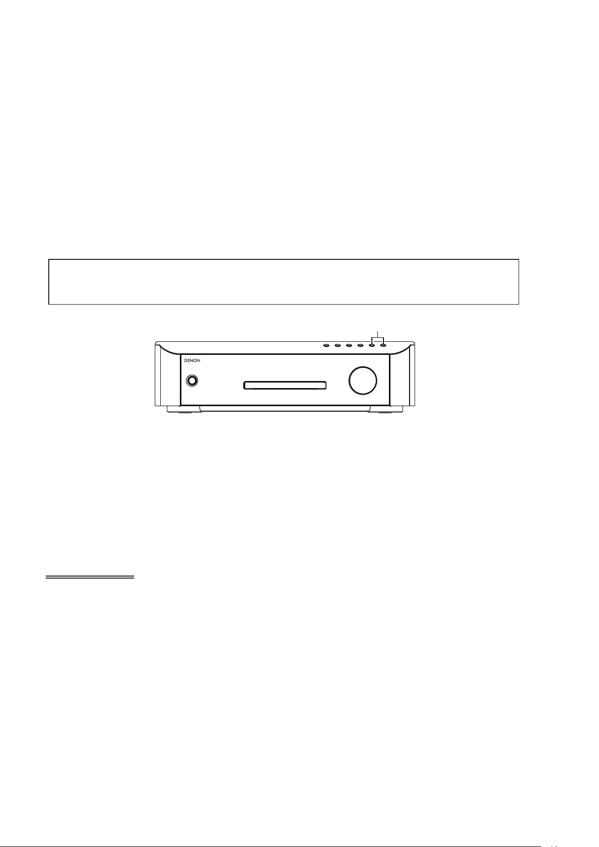
S-5BD
33 3
BLU-RAY DISC/DVD SURROUND RECEIVER
For purposes of improvement, specifi cations and design are subject to change without notice.
•
Please use this service manual with referring to the operating instructions without fail.
•
Some illustrations using in this service manual are slightly different from the actual set.
•
e
D&M Holdings Inc.
S0151V03DM/DG1009
Copyright 2010 D&M Holdings Inc. All rights reserved.
WARNING: Violators will be prosecuted to the maximum extent possible.
Page 2

SAFETY PRECAUTIONS
The following check should be performed for the continued protection of the customer and service technician.
LEAKAGE CURRENT CHECK
Before returning the unit to the customer, make sure you make either (1) a leakage current check or (2) a line to chassis
resistance check. if the leakage current exceeds 0.5 milliamps, or if the resistance from chassis to either side of the
power cord is less than 460 kohms, the unit is defective.
Be sure to test for leakage current with the AC plug in both polarities, in addition, in each power ON, OFF and STANDBY
mode, if applicable.
CAUTION
Please heed the points listed below during servicing and inspection.
◎Heed the cautions!
Spots requiring particular attention when servicing, such
as the cabinet, parts, chassis,etc., have cautions indicated
on l ab els. be sure to hee d the se ca usions and the
cautions indicated in the handling instructions.
◎Caution concerning electric shock!
(1) An AC voltage is impressed on this set, so touching
internal metal parts when the set is energized could
cause electric shoc k. Take care to avoid electric
shock, by for example using an isolating transformer
and gloves when servicing while the set is energized,
unplugging the power cord when replacing parts, etc.
(2) Tere are high voltage parts inside. Handle with extra
care when the set is energized.
◎ Caution concerning disassembly and
assembly!
Through great care is taken when manufacturing parts
from sheet metal, there may in some rare cases be burrs
on the edges of parts which could cause injury if ngers
are moved across them. Use gloves to protect your hands.
◎Only use designated parts!
The set's parts have spec if ic saf et y propert ie s (fire
resistance, voltage resistance, etc.). For replacement
par ts, be s u re to use par t s w hich hav e the sam e
poroperties. In particular, for the important safety parts
that are marked z on wiring diagrams and parts lists, be
sure to use the designated parts.
◎ Be sure to mount parts and arrange the wires
as they were originally!
For safety seasons, some parts use tape, tubes or other
insulating materials, and some parts are mounted away
from the surface of printed circuit boards. Care is also
taken with the positions of the wores omsode amd clamps
are used to keep wires away from heating and high
voltage parts, so be sure to set everything back as it was
originally.
◎Inspect for safety after servicing!
Ch eck that all s crews, par ts an d wires rem oved or
disconnected for servicing have been put back in their
original positions, inspect that no parts around the area
that has been serviced have been negatively affected,
con duct an i nsla tion chec k on th e e xter nal me tal
connectors and between the blades of the power plug,
and otherwise check that safety is ensured.
(Insulation check procedure)
Unplug the power cord from the power outlet, disconnect
the antenna, plugs, etc., and turn the power switch on.
Using a 500V insulation resistance tester, check that the
inplug and the externally exposed metal parts (antenna
terminal, headphones terminal, input terminal, etc.) is
1MΩ or greater. If it is less, the set must be inspected and
repaired.
CAUTION
Concerning important safety
parts
Many of the electric and structural parts used in the set
have sp ecial safety properties. In most ca ses these
properties are difficult to distinguish by sight, and using
replacement parts with higher ratings (rated power and
withstand voltage) does not necessarily guarantee that
safety performance will be poreserved. Parts with safety
properties are indicated as shown below on the wiring
diagrams and parts lists is this service manual. Be sure to
replace them with parts with the designated part number.
(1) Schematic diagrams ...... Indicated by the z mark.
(2) Parts lists ...... Indicated by the z mark.
Using parts other than the designated
parts could result in electric shock, res
or other dangerous situations.
2
Page 3
NOTE FOR SCHEMATIC DIAGRAM
NOTE FOR PARTS LIST
WARNING:
Parts marked with this symbol z have critical characteristics. Use ONLY replacement parts recommended by the manufacture
CAUTION:
Before returning the unit to the customer, make sure you make either (1) a leakage current check or (2) a line to chassis resistance check. If the
leakage current exceeds 0.5 milliamps, or if the resistance from chassis to either side of the power cord is less than 460 kohms, the unit is defective.
WARNING:
DO NOT return the unit to the customer until the problem is located and corrected.
NOTICE:
ALL RESISTANCE VALUES IN OHM. k=1,000 OHM / M=1,000,000 OHM
ALL CAPACITANCE VALUES IN MICRO FARAD. P=MICRO-MICRO FARAD EACH VOLTAGE AND CURRENT ARE MEASURED AT NO SIGNAL
INPUT CONDITION. CIRCUIT AND PARTS ARE SUBJECT TO CHANGE WITHOUT PRIOR NOTICE.
r.
NOTE FOR PARTS LIST
1.
Parts for which "nsp" is indicated on this table cannot be supplied.
2.
When ordering of part, clearly indicate "1" and "I" (i) to avoid mis-supplying.
3.
Ordering part without stating its part number can not be supplied.
4.
Part indicated with the mark "★" is not illustrated in the exploded view.
5.
Not including General-purpose Carbon Film Resistor in the P.W.Board parts list. (Refer to the Schematic Diagram for those parts.)
6.
Not including General-purpose Carbon Chip Resistor in the P.W.Board parts list. (Refer to the Schematic Diagram for those parts.)
WARNING:
● Resistors
Ex.: RN
* Resistance
Capacitors
●
Ex.: CE
* Capacity (electrolyte only)
* Capacity (except electrolyte)
・ When the dielectric strength is indicated in AC,"AC" is included after the dieelectric strength value.
Parts marked with this symbol z have critical characteristics. Use ONLY replacement parts recommended by the manufacturer.
Type
RD : Carbon
RC : Composition
RS : Metal oxide film
RW: winding
RN : Metal film
RK : Metal mixture
2
Indicates number of zeros after effective number.
2-digit effective number.
1-digit effective number.
: Units: ohm
Type
CE : Aluminum foil
electrolytic
CA : Aluminium solid
electrolytic
CS : Tantalum electrolytic
CQ : Film
CK : Ceramic
CC : Ceramic
CP : Oil
CM: Mica
CF : Metallized
CH : Metallized
2
Indicates number of zeros after effective number.
・ Units:μF.
・ Units:pF
2-digit effective number.
2
14K
Shape
and performance
2-digit effective number, decimal point indicated by R.
04W
Shape
and performance
Indicates number of zeros after efective number. (More than 2)
2-digit effective number.
2E
Power
2B : 1/8 W
2E : 1/4 W
2H : 1/2 W
3A : 1 W
3D : 2 W
3F : 3 W
3H : 5 W
1800ohm=1.8kohm1 8
1.2ohm1 R 2
1H
Dielectric
strength
0J : 6.3 V
1A : 10 V
1C : 16 V
1E : 25 V
1V : 35 V
1H : 50 V
2A : 100 V
2B : 125 V
2C : 160 V
2D : 200 V
2E : 250 V
2H : 500 V
2J : 630 V
2200μF2 2
2200pF=0.0022μF2 2
182
Resistance
F : ±1%
G : ±2%
J : ±5%
K : ±10%
M : ±20%
3R2
CapacityMAllowable
G
Allowable
error
P : Pulse-resistant type
NL : Low noise type
NB : Non-burning type
FR : Fuse-resistor
F : Lead wire forming
error
F : ±1%
G : ±2%
J : ±5%
K : ±10%
M : ±20%
Z : ±80%
: - 20%
P : +100%
C : ±0.25pF
D : ±0.5pF
= : Others
FR
Others
BP
Others
HS : High stability type
BP : Non-polar type
HR : Ripple-resistant type
DL : For change and discharge
HF : For assuring high requency
U : UL part
C : CSA part
W : UL-CSA part
F : Lead wire forming
2
・ Units:μF.
1
・ Units:pF
2.2μF2 R
1-digit effective number.
2-digit effective number, decimal point indicated by R
220pF2 2
Indicates number of zeros after effective numver. (0 or 1)
2-digit effective number.
3
Page 4
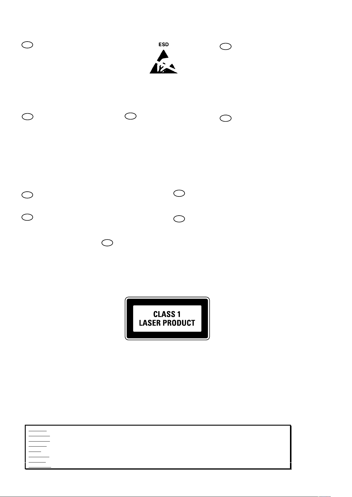
m
WARNING AND LASER SAFETY INSTRUCTIONS
GB
WARNING
All ICs and many other semi-conductors are
susceptible to electrostatic discharges (ESD).
Careless handling during repair can reduce
life drastically.
When repairing, make sure that you are
connected with the same potential as the
mass of the set via a wrist wrap with
resistance.
Keep components and tools also at this
potential.
F
ATTENTION
D
WARNUNG
I
WAARSCHUWING
AVVERTIMENTO
NL
Alle IC’s en vele andere halfgeleiders zijn
gevoelig voor elektrostatische ontladingen
(ESD).
Onzorgvuldig behandelen tijdens reparatie
kan de levensduur drastisch doen
verminderen.
Zorg ervoor dat u tijdens reparatie via een
polsband met weerstand verbonden bent met
hetzelfde potentiaal als de massa van het
apparaat.
Houd componenten en hulpmiddelen ook op
ditzelfde potentiaal.
Tous les IC et beaucoup d’autres semiconducteurs sont sensibles aux décharges
statiques (ESD).
Leur longévité pourrait être considérablement
écourtée par le fait qu’aucune précaution
n’est prise a leur manipulation.
Lors de réparations, s’assurer de bien être
relié au même potentiel que la masse de
l’appareil et enfiler le bracelet serti d’une
résistance de sécurité.
Veiller a ce que les composa
outils que l’on utilise soient également a ce
potentiel.
nts ainsi que les
GB
Safety regulations require that the set be restored to its original condition
and that parts which are identical with those specified be used.
NL
Veiligheidsbepalingen vereisen, dat het apparaat in zijn oorspronkelijke
toestand wordt terug gebracht en dat onderdelen, identiek aan de
gespecifieerde worden toegepast.
Alle IC und viele andere Halbleiter sind
empfindlich gegen elektrostatische
Entladungen (ESD).
Unsorgfältige Behandlung bei der Reparatur
kann die Lebensdauer drastisch vermindern.
Sorgen sie dafür, das Sie im Reparaturfall
über ein Pulsarmband mit Widerstand mit
dem Massepotential des Gerätes verbunden
sind.
Halten Sie Bauteile und Hilfsmittel ebenfalls
auf diesem Potential.
D
Bei jeder Reparatur sind die geltenden Sicherheitsvorschriften zu beachten.
Der Originalzustand des Gerats darf nicht verandert werden
Fur Reparaturen sind Original-Ersatzteile zu verwenden.
I
Le norme di sicurezza esigono che l’apparecchio venga rimesso nelle
condizioni originali e che siano utilizzati pezzi di ricambiago idetici a quelli
specificati.
Tutti IC e parecchi semi-conduttori sono
sensibili alle scariche statiche (ESD).
La loro longevita potrebbe essere fortemente
ridatta in caso di non osservazione della piu
grande cauzione alla loro manipolazione.
Durante le riparazioni occorre quindi essere
collegato allo stesso potenziale che quello
della massa dell’apparecchio tramite un
braccialetto a resistenza.
Assicurarsi che i componenti e anche gli
utensili con quali si lavora s
questo potenziale.
iano anche a
.
F
“Pour votre sécurité, ces documents
doivent être utilisés par des
spécialistes agrées, seu ls habilités à
réparer votre appareil en panne.”
Les normes de sécurité exigent que l’appareil soit remis a l’état d’origine et
que soient utilisées les pièces de rechange identiques à celles spécifiées.
LASER SAFETY
This unit employs a laser. Only a qualified service person should remove the cover or attempt to service t
device, due to possible eye injury.
his
USE OF CONTROLS OR ADJUSTMENTS OR PERFORMANCE OF PROCEDURE OTHER THAN THOSE
SPECIFIED H
EREIN MAY RESULT IN HAZARDOUS RADIATION EXPOSURE.
AVOID DIRECT EXPOSURE TO BEAM
WARNING
The use of optical instruments with this product will increase eye hazard.
Repair handling should take place as much as possible with a disc loaded inside the player
WARNING LOCATION: INSIDE ON LASER COVERSHIELD
CAUTION VISIBLE AND INVISIBLE LASER RADIATION WHEN OPEN AVOID EXPOSURE TO BEAM
ADVARSEL SYNLIG OG USYNLIG LASERSTRÅLING VED ÅBNING UNDGÅ UDS
ADVARSEL SYNLIG OG USYNLIG LASERSTRÅLING NÅR DEKSEL Å PNES UNNGÅ EKSPONERING FOR STRÅLEN
VARNING SYNLIG OCH OSYNLIG LASERSTRÅLNING NÄR DENNA DEL ÄR ÖPPNAD BETRAKTA EJ STRÅLEN
VARO! AVATT AESSA OLET ALTTIINA NÄKYVÄLLE JA NÄKYMÄTTÖMÄLLE LASER SÄ
VORSICHT SICHTBARE UND UNSICHTBARE LASERSTRAHLUNG WENN ABDECKUNG GEÖFFNET NICHT DEM STRAHL AUSSETSEN
DANGER VISIBLE AND INVISIBLE LASER RADIATION WHEN OPEN AVOID DIRECT EXPOSURE TO BEAM
ATTENTION RAYONNEMENT LASER VISIBLE ET INVISIBLE EN CAS D'OUVERTURE EXPOSITION DANGEREUSE AU FAISCEAU
Æ
TTELSE FOR STRÅLING
TEILYLLE. ÄLÄ KATSO SÄTEESEEN
030804ec
4
Page 5
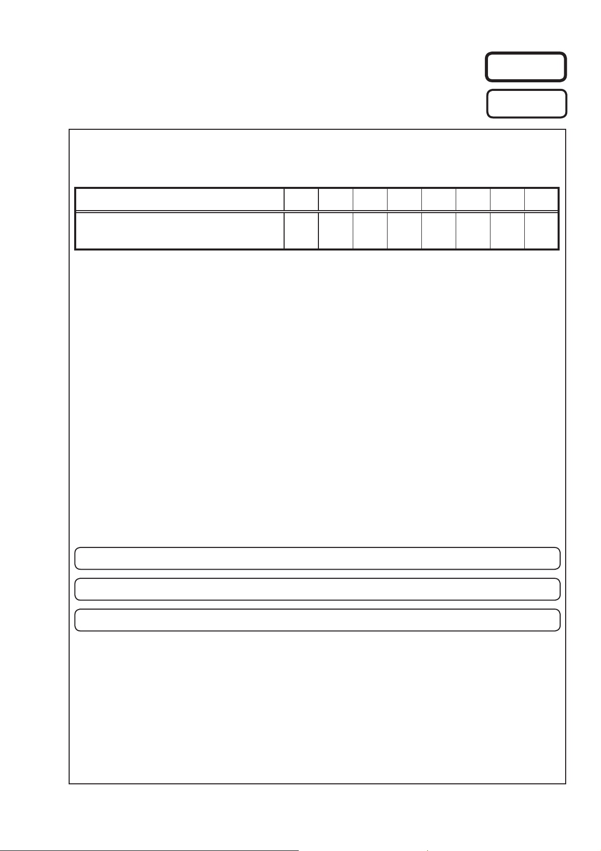
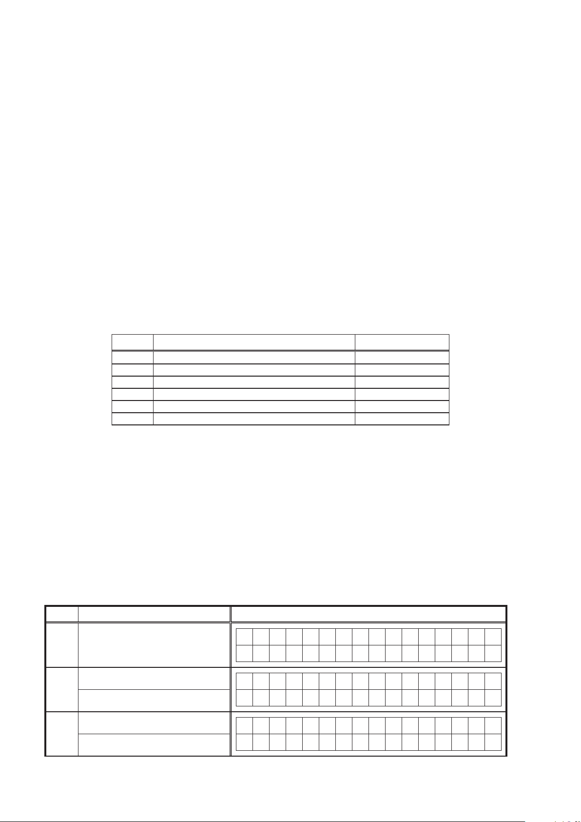
TECHNICAL SPECIFICATIONS
n Audio Section
• Power amplifier
Rated output :
Front : 75 W + 75 W (1 kHz, 4 Ω, T.H.D. 0.7 %)
Center : 75 W (1 kHz, 4 Ω, T.H.D. 0.7 %)
Surround : 75 W + 75 W (1 kHz, 4 Ω, T.H.D. 0.7 %)
Output connectors : Front, Center, Surround : 4 – 16 Ω
• Analog
Input sensitivity/Input impedance : 160 mV/47 kΩ
• Digital
Digital input : Format — Digital audio interface
n Video Section
• S-Video connectors
Input/output level and impedance :
Y (brightness) signal — 1 Vp-p, 75 Ω
C (color) signal — 0.3 (PAL)/0.286 (NTSC) Vp-p, 75 Ω
Frequency response : 5 Hz – 6 MHz — +0, –3 dB
n Tuner section
Reception frequency range :
[FM] 87.50 MHz – 108.00 MHz [AM]522 kHz – 1611 kHz
Receiving sensitivity :
[FM]1.5 μV / 75 Ω [AM]20 μV
FM stereo separation :
[FM]35 dB (1 kHz)
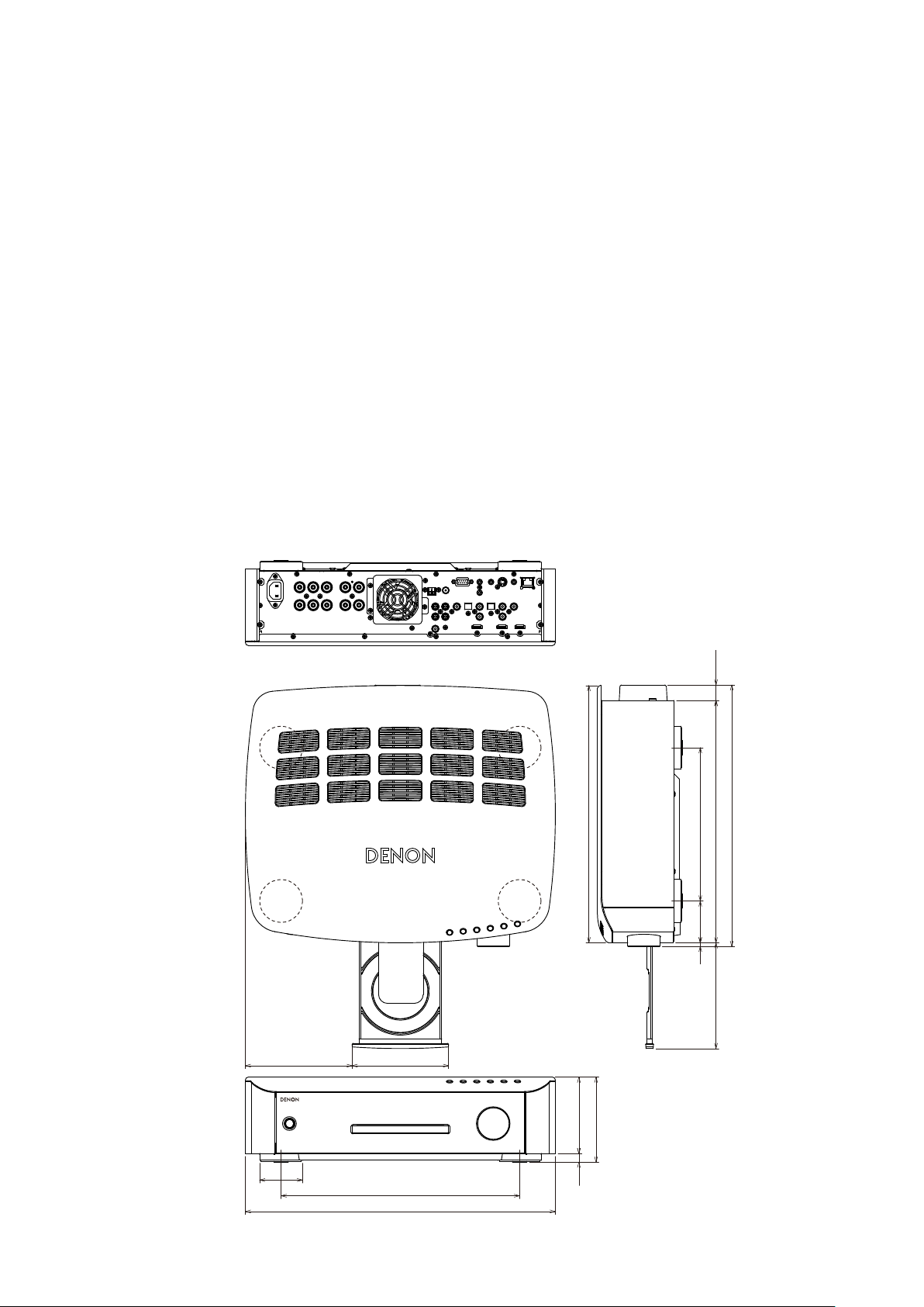
DIMENSION
n Applicable Discs/Memory Cards
BD-Video discs : 12 cm 1 side 1 layer, 12 cm 1 side 2 layers
DVD-Video discs :
12 cm 1 side 1 layer, 12 cm 1 side 2 layers/
12 cm 2 sides 2 layers (1 side 1 layer)
8 cm 1 side 1 layer, 8 cm 1 side 2 layers/
8 cm 2 sides 2 layers (1 side 1 layer)
Compact Discs (CD-DA) : 12 cm / 8 cm discs
Memory cards :
SD memory card/SDHC memory card/miniSD card/microSD card
n General
Power supply : AC 230 V, 50 Hz
Power consumption :
110 W
0.3 W (Normal standby)
Maximum external dimensions :
With the doors closed
434 (W) x 119 (H) x 365 (D) mm
With the doors open
445 (W) x 119 (H) x 365 (D) mm
Weight : 7.8 kg
n Remote Control Unit (RC-1122)
Batteries : R6/AA Type (two batteries)
Maximum external dimensions : 52 (W) x 243 (H) x 21 (D) mm
Weight : 175 g (including batteries)
360
135149.5
119
60
334
434
12 107
58.55 214.5
339148 21.8
365.8
5
Page 6
CAUTION IN SERVICING
Before the Digital P.W.B. are replaced
If you cannot specify the cause of the digital PWB defect, carry out "Initializing" → "Update to latest rmware".
The defect may be cleared.
• See the following for the method of initializing the μcom.
Initializing
S5BD initialization should be performed when the µcom, peripheral parts of µcom, Digital P.W.B., BE P.W.D and BD
mechanism are replaced.
1. Remove the power plug.
2. While pressing
3. Check that the entire display is ashing with an interval of about 1 second, and release your ngers from the 2
buttons and the microprocessor will be initialized.
Note: •If step 3 does not work, start over from step 1.
All user settings will be lost and this factory setting will be recovered when this initialization mode.
•
So make sure to m+emorize your setting for restoring after the initialization.
and SOURCE button simultaneously, plug the power cord into a power outlet.
9
2,3
Service tools
Measuring Disc: CD/TCD-784
DVD/VT502 or TDV-520A
BD/ABD-520 or BLX-108
Refer to "MEASURING METHOD AND WAVEFORMS".
z
Service Jigs
When you repair the printing board, you can use the following JIG (Extension cable kit). Please order to Denon Ofcial
Service Distributor in your region if necessary.
Extention cable kit
00D SPK- 562 TUCP CONN. JOINT KIT : 1 Set
6
Page 7
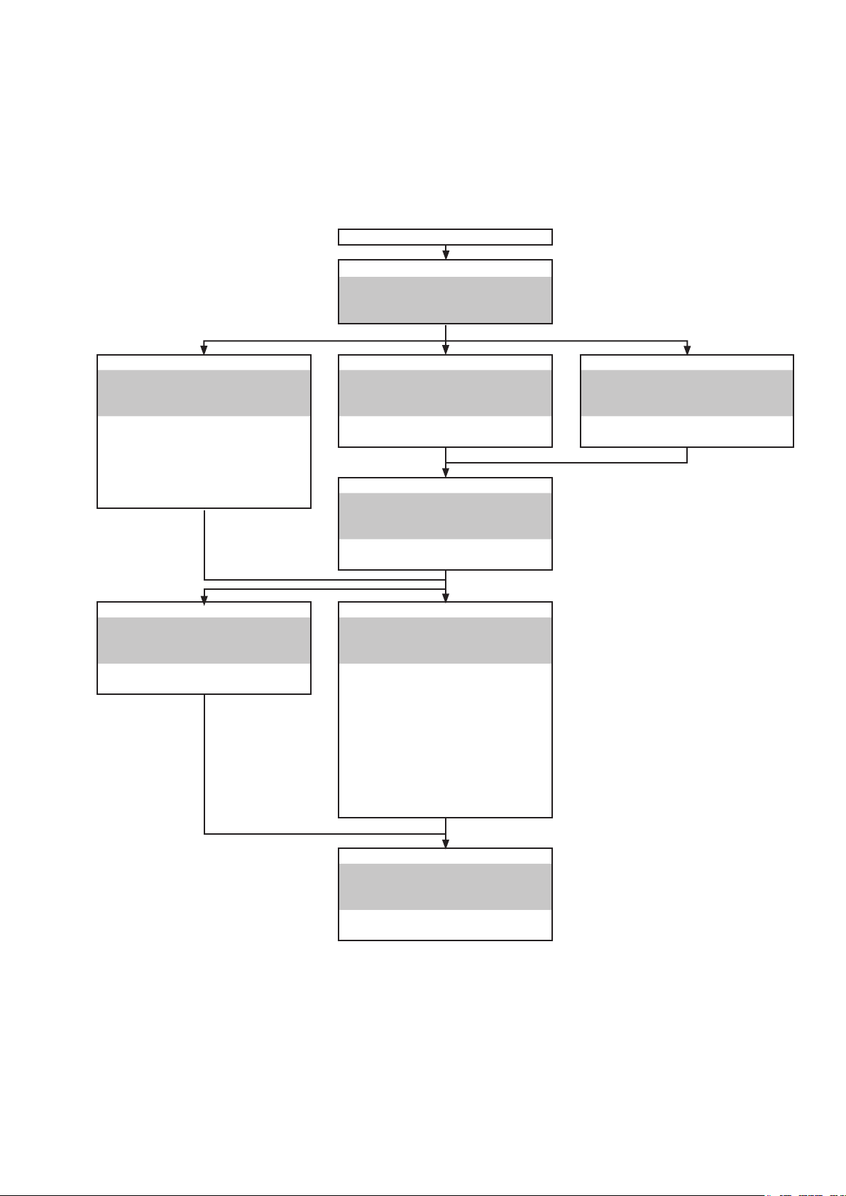
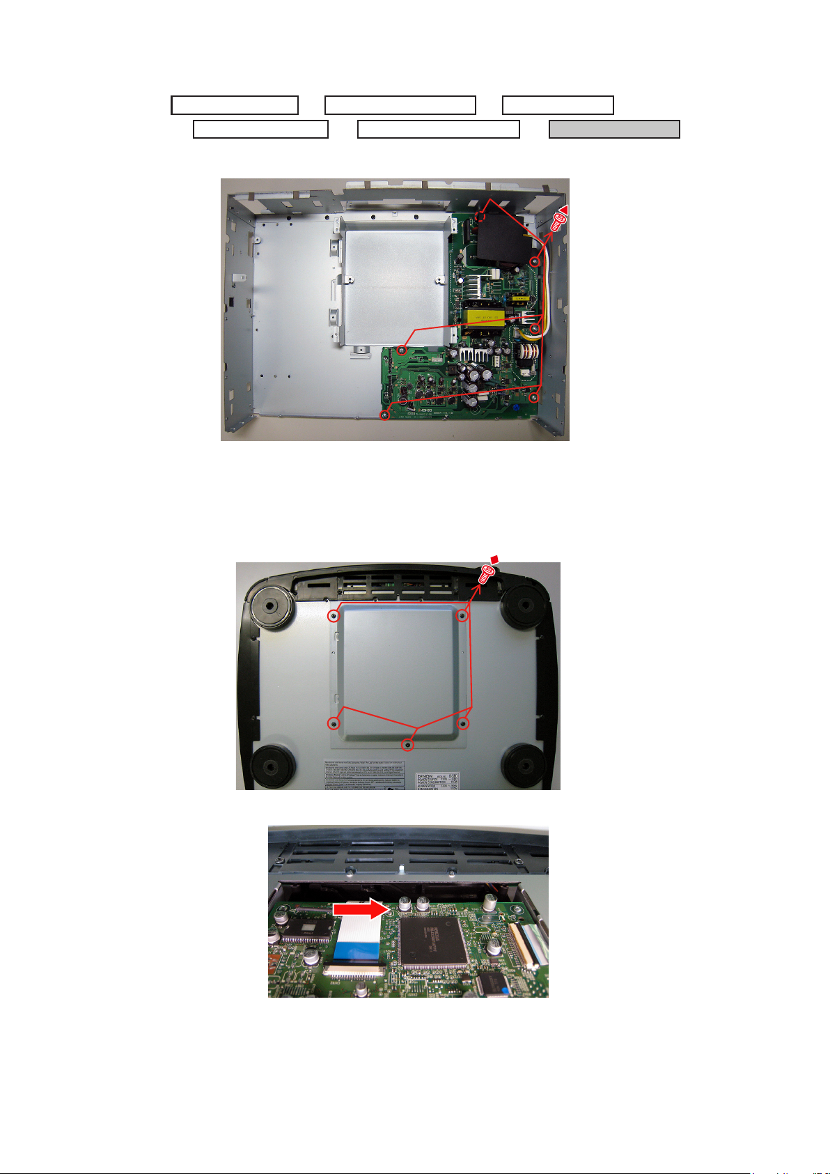
DISASSEMBLY
• Disassembleinorderofthearrowofthegureoffollowingow.
• Inthecaseofthere-assembling,assembleitinorderofthereverseofthefollowingow.
• Inthecaseofthere-assembling,observe"attentionofassembling"it.
• Ifwirebundlesareuntiedormovedtoperformadjustmentorpartsreplacementetc.,besuretorearrangethemneatly
astheywereoriginallybundledorplacedafterward.
Otherwise,incorrectarrangementcanbeacauseofnoisegeneration.
COVER SIDE-L/R
CABINET TOP ASSY
Referto "DISASSEMBLY
1.CABINET TOP ASSY"
and"EXPLODED VIEW"
FRONT PANEL ASSY BE UNIT ASSY DIGITAL AMP UNIT ASSY
Referto "DISASSEMBLY Referto "DISASSEMBLY Referto "DISASSEMBLY
2.PANEL FRONT SUB ASSY" 4. BE UNIT ASSY" 3. DIGITAL AMP UNIT ASSY"
and"EXPLODED VIEW" and"EXPLODED VIEW" and"EXPLODED VIEW"
ON/STUNIT B/EUNIT DIGITALAMPUNIT
(Ref.No.ofEXPLODEDVIEW:1-3) (Ref.No.ofEXPLODEDVIEW:5) (Ref.No.ofEXPLODEDVIEW:3-1)
FLDUNIT
(Ref.No.ofEXPLODEDVIEW:2-2)
F.USBUNIT CHASSIS MIDDLE
(Ref.No.ofEXPLODEDVIEW:3-2) Referto "DISASSEMBLY
5. CHASSIS MIDDLE"
and"EXPLODED VIEW"
CHASSISMIDDLE
(Ref.No.ofEXPLODEDVIEW:34)
MECHA ASSY CHASSIS BACK ASSY
Referto "DISASSEMBLY Referto "DISASSEMBLY
6. MECHA ASSY" 7. CHASSIS BACK ASSY"
and"EXPLODED VIEW" and"EXPLODED VIEW"
BDMECHAUNIT ANALOGAUDIOUNIT
(Ref.No.ofEXPLODEDVIEW:19) (Ref.No.ofEXPLODEDVIEW:1-2)
MAINUNIT
(Ref.No.ofEXPLODEDVIEW:2-1)
JOINTBUNIT
(Ref.No.ofEXPLODEDVIEW:2-3)
JOINTCUNIT
(Ref.No.ofEXPLODEDVIEW:3-5)
JOINTDUNIT
(Ref.No.ofEXPLODEDVIEW:3-6)
SMPS UNIT ASSY
Referto "DISASSEMBLY
8. SMPS UNIT ASSY"
and"EXPLODED VIEW"
SMPSUNIT
(Ref.No.ofEXPLODEDVIEW:1-1)
7
Page 8
About the photos used for descriptions in the DISASSEMBLY" section.
• Thedirectionfromwhichthephotographsusedhereinwerephotographedisindicatedat"Directionofphotograph:***"
attheleftoftherespectivephotographs.
• Refertothetablebelowforadescriptionofthedirectioninwhichthephotosweretaken.
• Photographsforwhichnodirectionisindicatedweretakenfromabovetheproduct.
The viewpoint of each photograph
(Photografy direction)
[View from above]
Direction of photograph: C
Direction of photograph: B
Front side
Direction of photograph: D
Direction of photograph: A
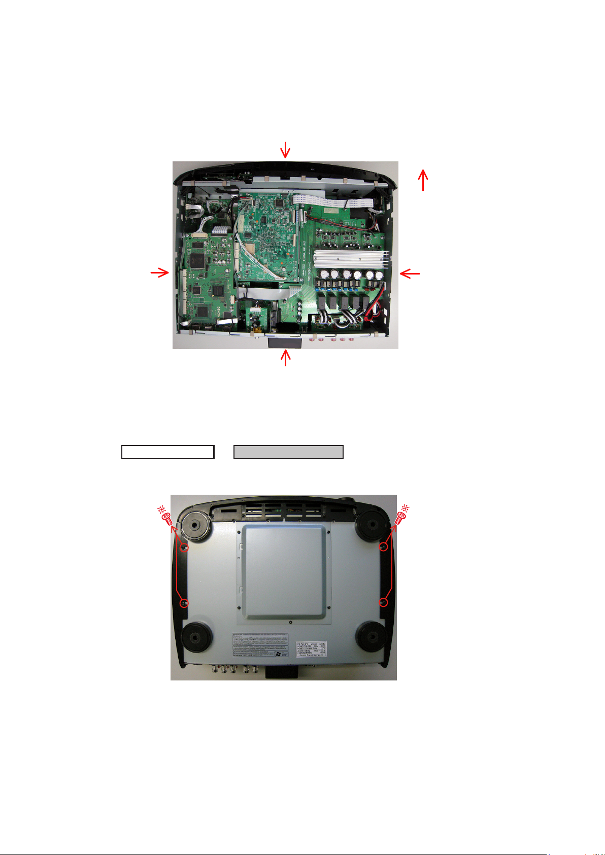
1. CABINET TOP ASSY
Proceeding :
(1) Removethescrews.
View from bottom
COVER SIDE-L/R
CABINET TOP ASSY
→
8
Page 9
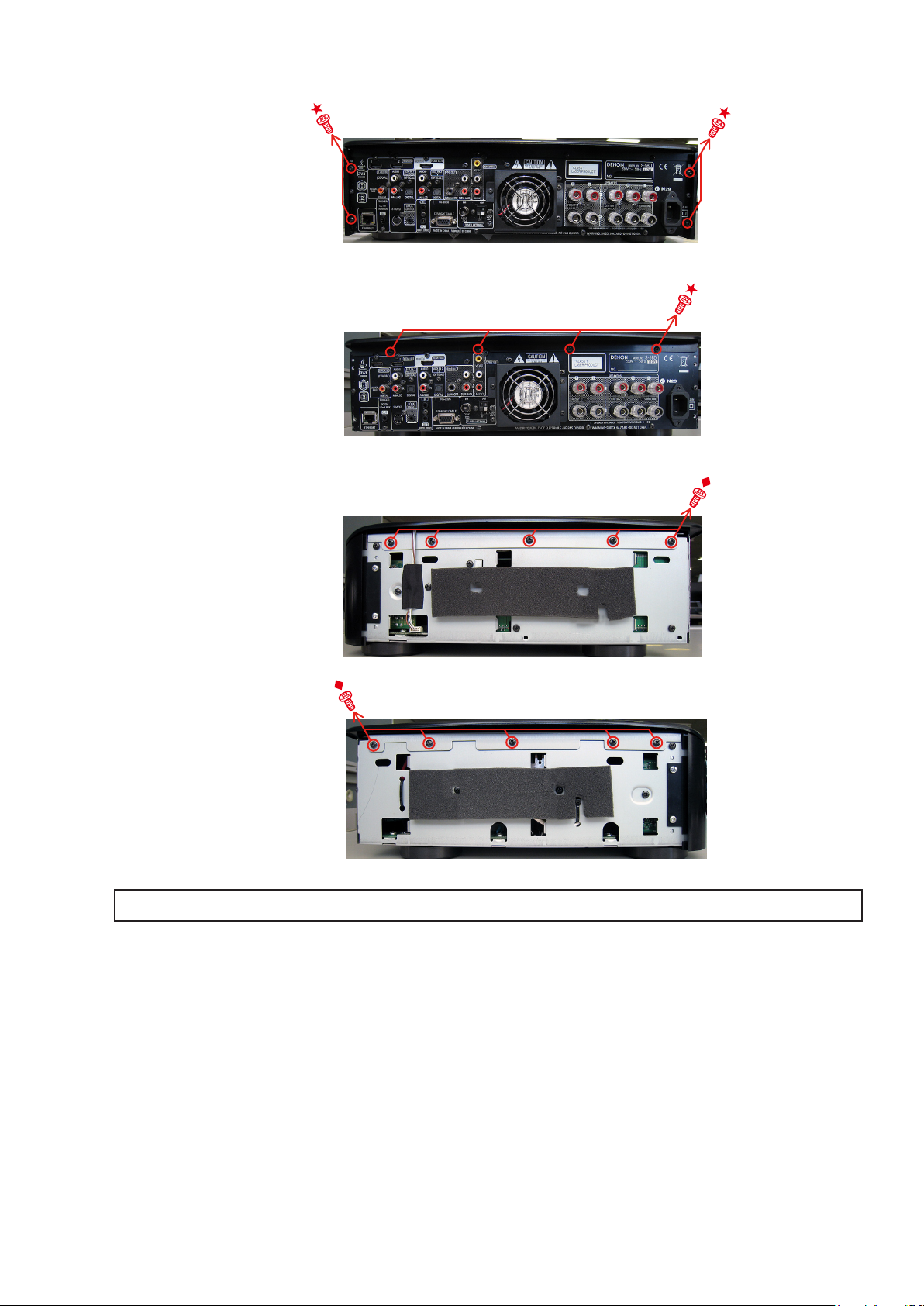
(2) RemovethescrewsandtheCoverSide.
Direction of photograph: A
(3) Removethescrews.
Direction of photograph: A
(4) Removethescrews.
Direction of photograph: C
Direction of photograph: D
Pleasereferto"EXPLODEDVIEW"forthedisassemblymethodofeachP.W.BincludedinCABINETTOPASSY.
9
Page 10
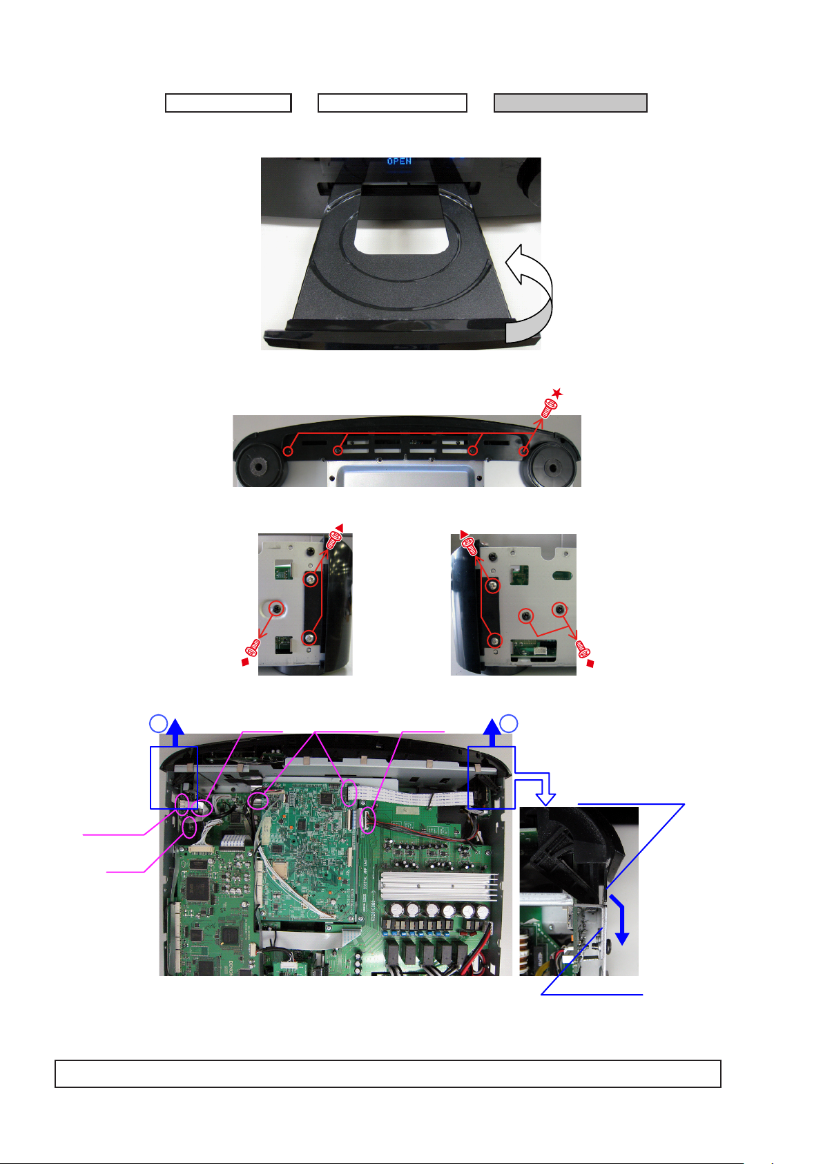
2. FRONT PANEL ASSY
Proceeding :
(1) RemovetheCoverTray.
Direction of photograph: B
(2) Removethescrews.
View from bottom
COVER SIDE-L/R
CABINET TOP ASSY
→
FRONT PANEL ASSY
→
(3) Removethescrews.
Direction of photograph: D
(4) DisconnecttheconnectorwireandFFCCable.
FFC CableCY054 CX104
FFC Cable
CY111
12
FRONT PANEL ASSY
zThe order of detaching FRONT PANEL ASSY are from q to w.
In the case of the re-assembling, install FRONT PANEL ASSY
in CHASSIS MAIN as shown in the photograph.
Pleasereferto"EXPLODEDVIEW"forthedisassemblymethodofeachP.W.BincludedinFRONTPANELASSY.
10
CHASSIS MAIN
Page 11
3. DIGITAL AMP UNIT ASSY
Proceeding :
(1) Removethescrews.DisconnecttheconnectorwiresandFFCCable.
COVER SIDE-L/R
DIGITAL AMP UNIT ASSY
CABINET TOP ASSY
→
DIGITAL AMP UNIT ASSY
→
CX104
CY044
CY047
FFC Cable
(2) Removethescrews.
Direction of photograph: A
CY035CY046
4. BE UNIT ASSY
Proceeding :
(1) Removethescrews.DisconnecttheconnectorwireandFFCCables.
COVER SIDE-L/R
CABINET TOP ASSY
→
BE UNIT ASSY
→
FFC Cable
BE UNIT ASSY
FFC Cable
FFC Cable
CX088
11
Page 12
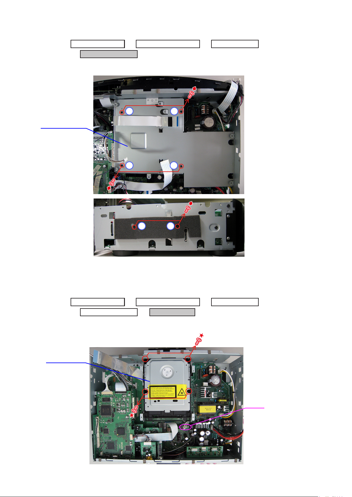
5. CHASSIS MIDDLE
→
→
Proceeding :
(1) Removethescrews.
CHASSIS MIDDLE
COVER SIDE-L/R
CHASSIS MIDDLE
→
CABINET TOP ASSY
→
1 5
4 6
BE UNIT ASSY
→
Direction of photograph: D
zIn the case of the re-assembling, assemble it in order from 1 to 6.
3 2
6. MECHA ASSY
Proceeding :
COVER SIDE-L/R
CHASSIS MIDDLE
(1) Removethescrews.Disconnecttheconnectorwire.
MECHA ASSY
CABINET TOP ASSY
→
MECHA ASSY
BE UNIT ASSY
→
CY063
12
Page 13
7. CHASSIS BACK ASSY
Proceeding :
(1) Removethescrews.Disconnecttheconnectorwire.
CHASSIS BACK ASSY
(2) Removethescrews.
COVER SIDE-L/R
CHASSIS MIDDLE
→
CABINET TOP ASSY
→
CHASSIS BACK ASSY
→
BE UNIT ASSY
→
CX191
CX234
CX032
Direction of photograph: A
(3) Removethescrews.
Direction of photograph: C
Pleasereferto"EXPLODEDVIEW"forthedisassemblymethodofeachP.W.BincludedinCHASSISBACKASSY.
13
Page 14
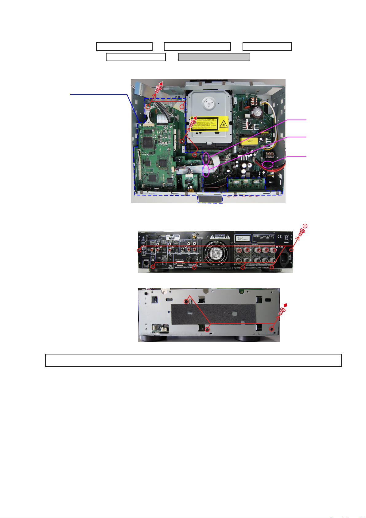
8. SMPS UNIT ASSY
Proceeding :
COVER SIDE-L/R
→
(1) Removethescrews.
→
CHASSIS MIDDLE
CABINET TOP ASSY
CHASSIS BACK ASSY
→
BE UNIT ASSY
→
→
SMPS UNIT ASSY
Removing discs
(1) Removethescrews.
View from bottom
(2) SlidetheSLIDECAMinthedirectionofthearrow.
Direction of photograph: A
(3) DrawouttheLOADERTRAY,thenremovethedisc.
14
Page 15
DIAGNOSTICS OF OPTICAL PICKUP AND REPLACING FE MAIN P.W.B AND BD MECHANISM UNIT ASSY
Make failure diagnostics of the Optical Pickup as follows.
If the laser drive current (Iop) becomes more than ±12[mA] of the initial value, the Optical Pickup should be replaced.
The laser drive current initial value is checked by "Iop checked Method" of next page.
In case of replacing the Pickup, change the whole part of the FE Main P.W.B and BD Mechanism Unit Assy.
No mechanical adjustment is necessary after the replacement.
Laser drive current initial value:
FL Display (The display part of 16 digits)
CD :
DVD :
BD(SL) :
BD(DL) :
1 2 3 4 5 6 7 8 9 10 11 12 13 14 15 16
T 2 1 - m m m m - n n n n
FL Display (The display part of 16 digits)
1 2 3 4 5 6 7 8 9 10 11 12 13 14 15 16
T 2 2 - m m m m - n n n n
FL Display (The display part of 16 digits)
1 2 3 4 5 6 7 8 9 10 11 12 13 14 15 16
T 2 3 - m m m m - n n n n
FL Display (The display part of 16 digits)
1 2 3 4 5 6 7 8 9 10 11 12 13 14 15 16
T 2 4 - m m m m - n n n n
Disc no read, unsteady playback, etc.
Laser drive current (Iop) check
HF wave form check
(Refer to WAVE FORMS)
Current value of the BD, DVD or CD IOP
is ± 12[mA] or more the initial value.
FE Main P.W.B. and BD Mechanism Unit
Assy replacing
15
Page 16
1. Iop checked Method
Select the laser ON/OFF(CD/DVD/BD)mode of the test mode, and check the IOP value of CD laser, DVD laser or BD
laser. (Refer to "6. Test mode")
FL Display (The display part of 16 digits)
1 2 3 4 5 6 7 8 9 10 11 12 13 14 15 16
T 2 L a s e r O n O f f
DVD laser current check
Press the 8 or 9 button to display the laser current value, and then select [X].
Check the current value of Iop (nnnn)
FL Display (The display part of 16 digits)
1 2 3 4 5 6 7 8 9 10 11 12 13 14 15 16
T 2 X - m m m m - n n n n
(X=1 : CD laser mode, 2 : DVD laser mode, 3 : BD(SL) laser mode, 4 : BD(DL) laser mode)
(nn.nn[mA] : Current value)
2. To clear the accumulated laser on time
Press the 1 button while the accumulated laser on time is displayed ("TC1, "TC2", "TC3" ) until "*" appears at the
fourth position. Press the 8 or 9 button to select "TC4". If the 1 button is pressed while "TC1" is displayed, the
accumulated laser on time of CD, DVD and BD is cleared
FL Display (The display part of 16 digits)
1 2 3 4 5 6 7 8 9 10 11 12 13 14 15 16
T C 4 * - - - - - - - - -
When "TC1", "TC2" or "TC3" is selected with the 8 or 9 button, "mmmmmm" is displayed as "0" so you can check.
FL Display (The display part of 16 digits)
1 2 3 4 5 6 7 8 9 10 11 12 13 14 15 16
T C V - - - m m m m m m h
(Y=1 : CD, 2 : DVD , 3 : BD, mmmmmm : Time(Fractions of hours are counted up one hour on the display.)
16
Page 17
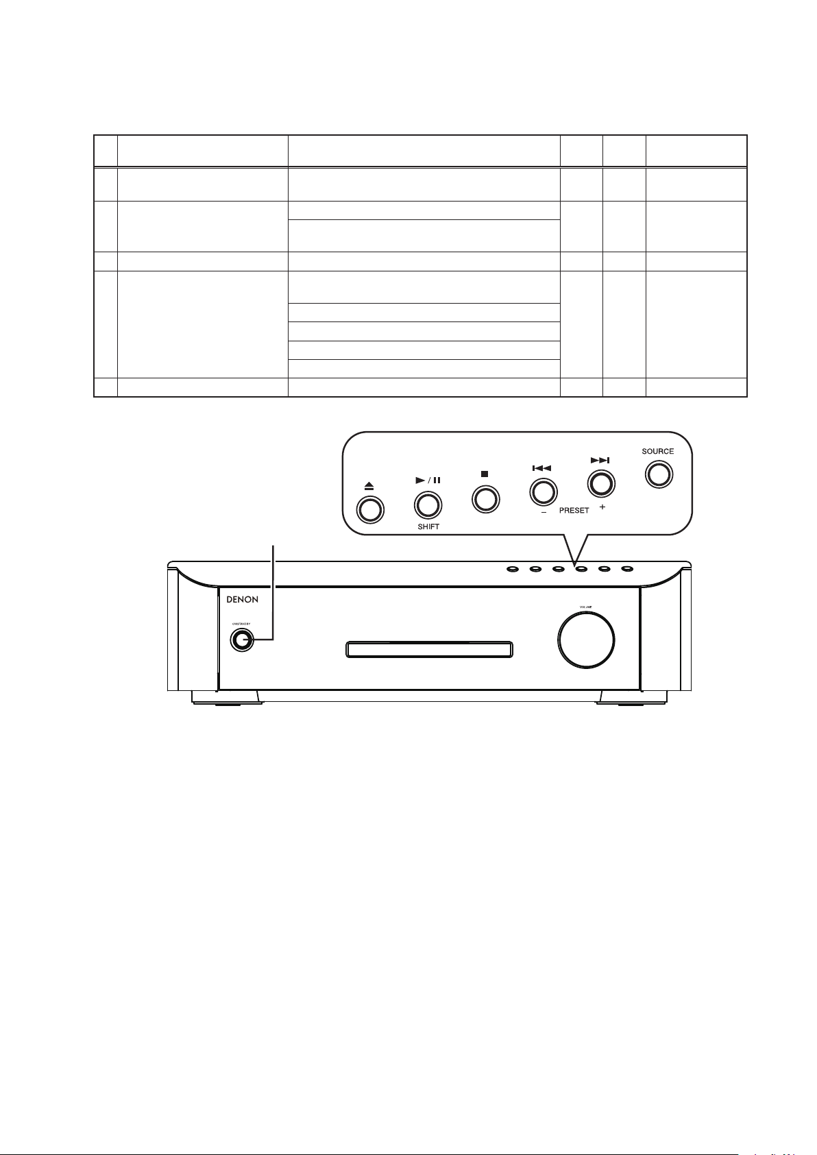
SERVICE MODE
s
Special mode setting button
No. Mode contents
1 Initialization mode
2 Heatrun & Version display mode
3 Displaying the protection history mode Displaying the protection history
4 KEY LOCK mode
5 Test mode Pickup & Dirve Test.
Backup data initialization is carried out.
(Remove settings for Network Setup.)
Opration Heat run mode
Serial No. and rmware versions such as Main, Sub, DSP
are displayed in the FL manager.
Operations using main unit panel buttons or master volume
are rejected.
Operations using main unit panel buttons are rejected
Panel lock mode is cancelled.
Operations using remote control are rejected.
Operations using Tray open are rejected.
ON/STANDBY
Button AButton
B
SOURCE
SOURCE
9
8
5 8
2 1/3
2 9
Entering the mode
ON/STANDBY button
AC cord
ON/STANDBY button
AC cord
AC cord
1. Initial setting mode
1.1. preparation
(1) Equipment used: None
(2) Unit setting: No spec other than the following procedure.
1.2. procedure
Initialize the BD player when µcom, peripheral parts of µcom, or MAIN P.W.B. unit has been replaced in servicing.
b
All user setting will be lost and its factory setting will be restored when this initialization is made. Be sure to memorize
b
your setting for restoring again after the initialization.
(1) Plug the AC cord into a power outlet.
(2) While pressing SOURCE and 9 buttons simultaneously, press the ON/STANDBY button. FL tube all lit.
(3) Release your ngers from the SOURCE and 9 buttons.
(4) The display on the FL tube switches to "INITIALIZING" / "Please_Wait" → "BD/SD" / "INITIALIZING" →
"BD/SD" / "INITIALIZED" and initialization is completed.
Afterwards, it enters the FIRST SETUP mode.
z
17
Page 18
2. Heat run & Version display mode
2.1. preparation
(1) Equipment used : Heat run disc (This operation may not work with any discs other than the heat run discs listed
below.)
CD : CD TEST DISC (TCD-HR01)
DVD
BD
(2) Unit setting : No spec other than the following procedure.
2.2. procedure
(1) While pressing the SOURCE and 8 buttons simultaneously, plug the AC cord into a power outlet.
2.3. Heat run mode
(1) Press the
(2) Set a disc to the tray and press the
operation starts.
DVD : After playback title-1 and title-10 of the disc, the tray opens and closes automatically, then playback the
CD/BD : The disc is played through once from title 1 through the last title, the tray opens and closes automatically,
(3) This heat run operation continues automatically or it stops caused by an error. In case of some error, the following
error messages are displayed on the FL tube.
button and open a tray.
5
title-1 and title-10 again.
then the disc is played through again from title 1 through the last title.
DVD TEST DISC (TDV-HR01)
:
BD TEST DISC (TBD-HR01)
:
button once . The "1" and "3" indicators blinks alternately and heat run
1
No. Error contents FL display
1 Tray Error ERROR 01
2 Bad Disc ERROR 02
3 Search Error ERROR 03
4 Read Error ERROR 04
5 Communications error ERROR 05
6 Other (Front end error) ERROR 06
2.4. Version display
When "No Disc", the FL display changes in the order given in item-2.5. Display Order each time you press the STATUS
button of remote control.
2.5. Display Order
Error information (Refer to 2.6. Error display)→q Model destination information → w Model Region information
→ e Main-μcom version information→ r Main1st Boot Loader → t DSPversion information / Audio PLD
→ y GUI FPGA Cong → u GUI Nios Program → i BD System-μcom version infomation
→ o BD System-μcom Gen number information → Q0 BD System-μcom Boot Loder → Q1 B/E version infomation
→ Q2 B/E Gen number information → Q3 B/E Boot Loder → Q4 B/E OS version information → Q5 F/E version information
→ Q6 F/E Gen number information → Q7 F/E Boot Loder → Q8 USB-μcom version information
XX : E1, E2, E3,etc X : A,B,C Y : 1, 2, 3, 4, 5, 6
No. Display item Display
q
w
e
Model destination
REGION BD
REGION DVD
Main-μcom
Main FLASH
S e r i a l N o . X X
R e g i o n B D : X
D V D : Y
M a i n : X X . X X
M a i n R O M : X X . X X
18
Page 19
No. Display item Display
Main 1st Boot Loder
r
Sub-μcom
DSP
t
Audio PLD
GUI FPGA
y
GUI Sash Nios
u
GUI Sash Font
BD System-μcom Version
i
BD System-μcom Date
BD System Gen
o
BD System-μcom Boot VersionVersion
Q0
BD System-μcom Boot Date
M a i n F B L : X X . X X
S u b : X X . X X
D S P : X X . X X
A u d i o P L D : X X X X
G U I C o n f i g :
X X X X X X X X
G U I P R G : X X X X X X X X
G U I D A T : X X X X X X X X
S y s V e r : X X X X X X
S y s D a y : X X X X X X
S y s G e n : X X X X X X
S y s B V e r : X X X X X X
S y s B D a y : X X X X X X
Q1
Q2
Q3
Q4
Q5
Q6
Q7
B/E Version
B/E Date
B/E Gen Number
B/E Boot Version
B/E Boot Date
B/E OS Version
B/E OS Date
F/E Verion
F/E Date
F/E Gen Number
F/E Boot Versoin
F/E Boot Date
B / E V e r : X X X X X X
B / E D a y : X X X X X X
B / E G e n : X X X X X X
B / E B V e r : X X X X X X
B / E B D a y : X X X X X X
B O S V e r : X X X X X X
B O S D a y : X X X X X X
F / E V e r : X X X X X X
F / E D a y : X X X X X X
F / E G e n : X X X X X X
F / E B V e r : X X X X X X
F / E B D a y : X X X X X X
USB-μcom Version
Q8
U S B : X X X
19
Page 20
2.6. Error display
See the following table for each "Error information" display and its contents (status). Display order is
Condition State Display
Sub-μcom NG No response from Sub-μcom
q
DIR NG No response from DIR
w
DSP1 NG
e
When DSP boot, executing DSP reset makes no change to DSP1 FLAGO port
"H".
No change to DSP1 FLAGO port "H" before issuing DSP command.
S U B E R R O R 0 1
D I R E R R O R 0 1
D S P 1 E R R O R 0 1
D S P 1 E R R O R 0 2
q,w,e,r,t
.
When DSP data read, executing WRITE="L" makes no change to ACK="H".
When DSP data read, executing REQ="L" makes no change to ACK="L".
When DSP data write, executing WRITE="H" makes no change to ACK="H".
When DSP data write, executing REQ="L" makes no change to ACK="L".
When DSP special code boot, executing DSP reset makes no change to DSP1
FLAGO port "H".
No change to DSP1 FLAGO port "H" before issuing DSP special read
command.
No change to DSP1 FLAGO port "H" before DSP version read.
EEPROM NG Error appeared in EEPROM checksum.(*** is a block address number.)
r
Both SUB/DSP/
t
EEPROM OK
D S P 1 E R R O R 0 3
D S P 1 E R R O R 0 4
D S P 1 E R R O R 0 5
D S P 1 E R R O R 0 6
D S P 1 E R R O R 1 1
D S P 1 E R R O R 1 2
D S P 1 E R R O R 1 3
E 2 P R O M E R R * * *
(No error display, version display only)
20
Page 21

3. Displaying the protection history mode
3.1. preparation
(1) Equipment used: None
(2) Unit setting: No spec other than the following procedure.
3.2. procedure
(1) Plug the AC cord into a power outlet.
(2) While pressing 5 and 8 buttons simultaneously, press the ON/STANDBY button to turn the power on.
The error (protection history display) mode is set.
(3) Press the STATUS button of remote control to turn on the FL display.
3.3. About the display on the FL display
When the STATUS button of remote control is pressed after setting the error (protection history display) mode, a history
like the one shown below is displayed, depending on the conditions.
(1) Normally (when there has been no protection incident)
P R O T E C T H I S T O R Y
: N O P R O T E C T
(2) For SP DC (when the last protection incident was SP DC protection)
P R O T E C T H I S T O R Y
: S P O U T _ D C
(3) For AMP SD (when the last protection incident was AMP SD protection)
P R O T E C T H I S T O R Y
: D A M P E R R
(4) For POWER DC (when the last protection incident was POWER DC protection)
P R O T E C T H I S T O R Y
: 2 n d - P o w D C
When the STATUS button of remote control. is pressed again after the above protection history is displayed, the normal
display reappears.
21
Page 22
3.4. Clearing the protection history
There are two ways to clear the protection history, as described below.
(1) Start up the error (protection history display) mode, display the error, then press and hold in the
seconds.
P R O T E C T H I S T O R Y
: S P O U T _ D C
Press and hold in the 2 button for 3 seconds.
P R O T E C T H I S T O R Y
C L E A R
The above is displayed and the protection history is cleared.
P R O T E C T H I S T O R Y
: N O P R O T E C T
button for 3
2
(2) Initialize. (See 1.Initial setting mode)
If you want to save a backup of other setting item, use the method in 3.4.(1) above.
z
s
s
Warning indication by the STANDBY LED
If the power is turned off when a protection incident has been detected, the STANDBY LED (red) ashes as follows as
warning according to the conditions in which the protection incident occurred.
(1) SP DC PROTECTION/AMP SD PROTECTION : Flashes in cycles of 2 seconds (1 second lit, 1 second off)
(2) POWER DC PROTECTION : Flashes in cycles of 0.5 seconds (0.25 seconds lit, 0.25 seconds off)
1 Accepting input from the ON/STANDBY,
b
2 Even if the AC cord is disconnected and then reconnected, the unit starts in 0.25-second interval ashing mode.
b
The accepting of input from the ON/STANDBY, 1, and 5 buttons is also prohibited in that case.
, and 5 buttons is prohibited.
1
1, b2
b
3.5. Recovering from POWER DC PROTECTION
(1) When POWER DC PROTECT is detected, press the ON/STANDBY button while pressing the
the unit simultaneously.
(2) The STANDBY LED (red) stops ashing and the unit enters the normal standby mode.
2
and
buttons on
1/3
22
Page 23

4. KEY LOCK mode
4.1. preparation
(1) Equipment used: None
(2) Unit setting: No spec other than the following procedure.
4.2. procedure
(1) While pressing 2 and
(2) "KEY_LOCK_MODE" is displayed on the FL tube. This sets the KEY LOCK mode.
buttons simultaneously, plug the AC cord into a power outlet.
1/3
K E Y L O C K M O D E
p r e s s a n y k e y
4.3. KEY LOCK mode(with Master Volume)
(1) While the indication of section 4.2 is displayed on the FL tube, press the
(2) "Key_Lock_w/_VR" is displayed on the FL tube. This sets the KEY LOCK mode (with Master Volume).
9
button.
K e y L o c k w / V R
4.4. KEY LOCK mode (without Master Volume)
(1) While the indication of section 4.2 is displayed on the FL tube, press the
(2) "Key_Lock_w/o_VR" is displayed on the FL tube. This sets the KEY LOCK mode (without Master Volume).
8
button.
K e y L o c k w / o V R
4.5. REMOTE LOCK mode
(1) While the indication of section 4.2 is displayed on the FL tube, press the
(2) "Remote_Lock" is displayed on the FL tube. This sets the REMOTE LOCK mode.
1/3
button.
R e m o t e L o c k
4.6. TRAY LOCK mode
(1) While the indication of section 4.2 is displayed on the FL tube, press the SOURCE button.
(2) "Tray_Lock" is displayed on the FL tube. This sets the REMOTE LOCK mode.
T r a y L o c k
4.7. KEY LOCK mode cansel
(1) Plug the AC cord into a power outlet.
(2) While pressing 2 and
mode.
(3) While the indication of section 4.2 is displayed on the FL tube, press the
(4) "CLEAR" is displayed on the FL tube, each mode in sections 4.3., 4.4., 4.5., and 4.6. is cancelled.
buttons simultaneously, plug the AC cord into a power outlet. This sets the KEY LOCK
1/3
button.
2
C L E A R
23
Page 24
5. Test mode
5.1. Entering the test mode
The test mode is entered by pressing the 2 and 9 buttons simultaneously, plug the AC cord into a power outlet.
FL tube display when test mode entered
FL Display (The display part of 16 digits)
1 2 3 4 5 6 7 8 9 10 11 12 13 14 15 16
T E S T M O D E
When the test mode is set, a color bar appears on the monitor.
5.2. Selecting the mode
The following modes are available.
・
(1) Laser on/off (CD/DVD/BD) mode : T2
(2) Servo adjustment value display mode : T3
(3) Error rate (skew) measurement mode : T7
(4) Accumulated laser on time display mode : TC
(5) Track buffer output mode : TE
(6) Picking up No. display mode : TG
(7) Error log display mode : TH
(8) Test mode cancel : TI
When the
q
button is pressed after entering the test mode, the display switches in the order: "T2, T3, T7, TC, TE,
9
TG, TH, TI, T2 …"
FL Display (The display part of 16 digits)
1 2 3 4 5 6 7 8 9 10 11 12 13 14 15 16
T 2 L a s e r O n O f f
FL Display (The display part of 16 digits)
1 2 3 4 5 6 7 8 9 10 11 12 13 14 15 16
T 3 S e r v o A d j .
FL Display (The display part of 16 digits)
1 2 3 4 5 6 7 8 9 10 11 12 13 14 15 16
T 7 E r r o r R a t e
FL Display (The display part of 16 digits)
1 2 3 4 5 6 7 8 9 10 11 12 13 14 15 16
T C L a s e r O n T i m
FL Display (The display part of 16 digits)
1 2 3 4 5 6 7 8 9 10 11 12 13 14 15 16
T E T r a c k B u f
FL Display (The display part of 16 digits)
1 2 3 4 5 6 7 8 9 10 11 12 13 14 15 16
T G O P U N u m b e r
FL Display (The display part of 16 digits)
1 2 3 4 5 6 7 8 9 10 11 12 13 14 15 16
T H E r r o r L o g
FL Display (The display part of 16 digits)
1 2 3 4 5 6 7 8 9 10 11 12 13 14 15 16
T I T e s t E x i t
When the
w
position (for example, if currently at "TI", it switches as follows: "TH, TG,
button is pressed, the display switches in the opposite order fromq above, starting from the current
8
24
TE, TC, T7, T3, T2, TI, TH …").
s
Page 25
5.3. About each mode
With the mode selected, press the 1 button to set that mode.
・
(1) Laser on/off (CD/DVD/BD) mode
Press the 8 or 9 button to select [X] and press the 1 button to set it.
Laser on/off control is executed and the laser current is displayed.
FL Display (The display part of 16 digits)
1 2 3 4 5 6 7 8 9 10 11 12 13 14 15 16
T 2 X m m m m n n n n
(X=1 : CD laser mode, 2 : DVD laser mode, 3 : BD(SL) laser mode, 4 : BD(DL) laser mode)
(mm.mm[mA] : Stored data, nn.nn[mA] : Current value)
When the current value is more that ± 12.00[mA] of saved data, it becomes the pickup transducer's target.
b
In this case, replace the mechanism unit.
If stored value is not
FL Display (The display part of 16 digits)
1 2 3 4 5 6 7 8 9 10 11 12 13 14 15 16
T 2 X - - - - - - n n n n
(X=1 : CD laser mode, 2 : DVD laser mode, 3 : BD(SL) laser mode, 4 : BD(DL) laser mode)
(nn.nn[mA] : Current value)
When the 2 button is pressed, the layer above the current layer is displayed. See "5.4 Stopping the mode".
(2) Servo adjustment value display mode
Press the 8 or 9 button to select [XXX]. Refer to [Table 1 - Servo adjustment value display mode details].
FL Display (The display part of 16 digits)
1 2 3 4 5 6 7 8 9 10 11 12 13 14 15 16
T X X X
(XXX : Servo adjustment value
Press the 1 button to set. The contents indicated on "Table 1: Details of the servo adjustment value display mode"
are displayed.
FL Display (The display part of 16 digits)
1 2 3 4 5 6 7 8 9 10 11 12 13 14 15 16
)
T X X X m m m m m m n n
(XXX : Selection mode, mmmmmm : Address(HEX), nn:Data(HEX))
The rst time, the address speciciation position is the uppermost position (5th place). The address speciciation
position moves downwards each time the 1 button is pressed.
The address speciciation position ashes (at an interval of about 0.5 seconds). If the 1 button is pressed after
moving to the lowermost position (10th place), the position moves to the uppermost position
Use the 8 or 9 button to change the display at the address specication position.
When the 2 button is pressed, the layer above the current layer is displayed. See "5.4 Stopping the mode".
25
Page 26
(3) Error rate measurement mode
Press the 8 or 9 button to select [YY] .
Refer to [Table 2 - Error rate details].
FL Display (The display part of 16 digits)
1 2 3 4 5 6 7 8 9 10 11 12 13 14 15 16
T Y Y F F F F F F F F F F
(X : measurement mode, F : Address and error rate (When not set, "F" is displayed.)
Press the 1 button to begin error rate measurement. The address and error rate are displayed.
For a description of the displayed measurement results, see "Table 2: Error rate details".
FL Display (The display part of 16 digits)
1 2 3 4 5 6 7 8 9 10 11 12 13 14 15 16
T Y Y m m m m m m | | | |
(YY : selection mode [71 to 94], m : address [PBA][HEX], l : error rate [COUNT/SEC] [HEX])
(Note) CD (4x-speed) : Renewal of data is carried out for every 300 frame.
Error rate of 75 frames is displayed.
DVD (2x-speed) : Renewal of data is carried out for every 80ECC block.
Error rate of 8ECC block is displayed.
BD (2x-speed) : Renewal of data is carried out for every 136LDC clusters block.
Error rate of 8LDC clusters block is displayed.
The mode chosen when selection mode was changed into the trace execution and the 1 button was pushed is
performed from the beginning.
When the 1 button is pushed without changing selection mode, the mode under selection is performed from the
beginning.
(If the 1 button is pushed, the address corresponding to the chosen mode will be searched again.)
The pause mode is set after tracing is completed.
When the 2 button is pressed, the layer above the current layer is displayed. See "5.4 Stopping the mode".
(4) Accumulated laser on time display mode
Press the 8 or 9 button to select [Y] and press the 1 button to set it.
The accumulated laser on time is displayed.
FL Display (The display part of 16 digits)
1 2 3 4 5 6 7 8 9 10 11 12 13 14 15 16
T C Y m m m m m m h
(Y=1 : CD, 2 : DVD , 3 : BD, mmmmmm : Time(Fractions of hours are counted up one hour on the display.)
When the 2 button is pressed, the layer above the current layer is displayed. See "5.4 Stopping the mode".
---To clear the accumulated laser on time---
Press the 1 button while the accumulated laser on time is displayed ("TC1, "TC2", "TC3" ) until "*" appears at
the fourth position.
FL Display (The display part of 16 digits)
1 2 3 4 5 6 7 8 9 10 11 12 13 14 15 16
T C Y * m m m m m m
Press the 8 or 9 button to select "TC4"
FL Display (The display part of 16 digits)
1 2 3 4 5 6 7 8 9 10 11 12 13 14 15 16
T C 4 *
If the 1 button is pressed while "TC4" is displayed, the accumulated laser on time of CD, DVD and BD is cleared.
FL Display (The display part of 16 digits)
1 2 3 4 5 6 7 8 9 10 11 12 13 14 15 16
T C 1 0 0 0 0 0 0 h
When "TC1", "TC2" or "TC3" is selected with the 8 or 9 button, "mmmmmm" is displayed as "0" so you can
check.
26
Page 27
(5) Track buffer output mode
Press the 8 or 9 button to select "Y" and switch the track buffer output.
FL Display (The display part of 16 digits)
1 2 3 4 5 6 7 8 9 10 11 12 13 14 15 16
T E Y T r a c k B u f f
(Y=1 : Track buffer being output, 0 : Track buffer output off )
When the 2 button is pressed, the layer above the current layer is displayed. See "5.4 Stopping the mode".
(6) Picking up No. display mode
Press the 8 or 9 button to switch to the pickup number display.
The pickup number is a 14-digit number, so it is displayed in two sections.
FL Display (The display part of 16 digits)
1 2 3 4 5 6 7 8 9 10 11 12 13 14 15 16
T G X Y Y Y Y Y Y Y
(X (display position) = 1 : Lower digits, 2 : Upper digits. YYYYYYY: Pickup number)
When the 2 button is pressed, the layer above the current layer is displayed. See "5.4 Stopping the mode".
(7) Error log display mode
Press the 8 or 9 button to switch to the error log display.
For Error log No. and description of the displayed measurement results, see "Table 3: Error log details".
FL Display (The display part of 16 digits)
1 2 3 4 5 6 7 8 9 10 11 12 13 14 15 16
n T H X
(n : Error information No.(1~5), X : Error log No.)
Display when there is no error
FL Display (The display part of 16 digits)
1 2 3 4 5 6 7 8 9 10 11 12 13 14 15 16
n T H 1 N o E r r o r
When the 2 button is pressed, the layer above the current layer is displayed. See "5.4 Stopping the mode".
(8) Test mode cancel
A conrmation message is displayed. Press the 1 button to set, canceling the test mode.
FL Display (The display part of 16 digits)
1 2 3 4 5 6 7 8 9 10 11 12 13 14 15 16
T I 1 R e a l l y ?
When the 2 button is pressed, the layer above the current layer is displayed. See "5.4 Stopping the mode".
27
Page 28

5.4. Stopping the mode
When the 2 button is pressed, the layer above the current layer is displayed. The relationship between the different
modes and the display of the different layers is shown on the table below.
Mode 1 layer 2 layer 3 layer
Laser on/off (CD/DVD/BD) mode T2 LaserOnOff T2X mmmm nnnn Non
Servo adjustment value display mode T3 Servo Adj. TXXX TXXXmmmmmm nn
Error rate (skew) measurement mode T7 Error Rate TYYFFFFFFFFFF TYYmmmmmmllll
Accumulated laser on time display mode TC LaserOnTim TCY mmmmmmh
Track buffer output mode TE Track Buf TEYTrack Buff Non
Picking up No. display mode TG OPU Number TGX YYYYYYY Non
Error log display mode TH Error Log
Test mode cancel TI Test Exit TI1 Really? Non
nTHX
nTH1 No Error
TCY* mmmmmmh
TC4*
nTHX dddddd
nTHAyyy dddd
5.5. About the OPEN/CLOSE (
)button
5
Even during the test mode, the tray is opened and closed when the 5 button is pressed.
5.6. Test mode detailed table
Table 1: Servo adjustment value display mode details
No XXX Name Address range Meaning
0 T30 BUF_ID_SDRAM 0x000000~0x3FFFFF SDRAM
1 T31 BUF_ID_MPU_ALL 0x000000~0xBEFF3F MPU(Abs Access)
2 T32 BUF_ID_MPU_RMCR 0x000000~0x00FFFF ROMCOR
3 T33 BUF_ID_MPU_SYSCFG 0x000000~0x000FFF SystemCongration
4 T34 BUF_ID_MPU_DMAC 0x000000~0x0004FF DMAC
5 T35A BUF_ID_MPU_ITIM0 0x000000~0x0000FF ITIM 0
6 T35B BUF_ID_MPU_ITIM1 0x000000~0x0000FF ITIM 1
7 T35C BUF_ID_MPU_ITIM2 0x000000~0x0000FF ITIM 2
8 T35D BUF_ID_MPU_ITIM3 0x000000~0x0000FF ITIM 3
9 T35E BUF_ID_MPU_ITIM4 0x000000~0x0000FF ITIM 4
10 T35F BUF_ID_MPU_ITIM5 0x000000~0x0000FF ITIM 5
11 T36 BUF_ID_MPU_RSV2 0x000000~0x0079FF Reserved
12 T37 BUF_ID_MPU_WDT 0x000000~0x000FFF WDT
13 T38 BUF_ID_MPU_UART0 0x000000~0x0000FF UART 0
14 T39 BUF_ID_MPU_UART1 0x000000~0x0000FF UART 1
15 T40 BUF_ID_MPU_CSIO0 0x000000~0x0000FF CSIO 0
16 T41 BUF_ID_MPU_CSIO1 0x000000~0x0000FF CSIO 1
17 T42 BUF_ID_MPU_GPIO0 0x000000~0x0000FF GPIO 0
18 T43 BUF_ID_MPU_GPIO1
19 T44 BUF_ID_MPU_GPIO2 0x000000~0x0000FF GPIO 2
20 T45 BUF_ID_MPU_RSV5 0x000000~0x00BCFF Reserved
21 T46 BUF_ID_MPU_HEXBIU 0x000000~0x000FFF HEXBIU
22 T47 BUF_ID_MPU_HCSC 0x000000~0x000FFF HCSC
23 T48 BUF_ID_MPU_RSV6 0x000000~0x7DDFFF Reserved
24 T49 BUF_ID_MPU_RSV7 0x000000~0x3DFEFF Reserved
25 T50 BUF_ID_MPU_INT 0x000000~0x00003F INT
26 T51 BUF_ID_IRAM 0x000000~0x003FFF IRAM(internal SRAM))
27 T52 BUF_ID_DSP 0x000000~0x001FFF DSP Register
28 T53 BUF_ID_AFE 0x000000~0x0000FF AFE Register
29 T54 BUF_ID_SVO_ALL 0x000000~0x001FFF SVO REG ABS ACCESS
30 T55 BUF_ID_SVO_REG 0x000000~0x0007FF SVERVO REG
0x000000~0x0000FF GPIO 1
28
Page 29
No XXX Name Address range Meaning
31 T56 BUF_ID_SVO_SVRAM 0x000000~0x0005FF SVRAM
32 T57A BUF_ID_SVO_CRAM0 0x000000~0x0001FF CRAM0
33 T57B BUF_ID_SVO_CRAM1 0x000000~0x0001FF CRAM1
34 T57C BUF_ID_SVO_CRAM2 0x000000~0x0001FF CRAM2
35 T57D BUF_ID_SVO_CRAM3 0x000000~0x0001FF CRAM3
36 T58A BUF_ID_SVO_ZRAM0 0x000000~0x0001FF ZRAM0
37 T58B BUF_ID_SVO_ZRAM1 0x000000~0x0001FF ZRAM1
38 T58C BUF_ID_SVO_ZRAM2 0x000000~0x0001FF ZRAM2
39 T58D BUF_ID_SVO_ZRAM3 0x000000~0x0001FF ZRAM3
40 T59 BUF_ID_EPRM 0x000000~0x000FFF EEPROM
41 T60 BUF_ID_PUCONT_LDD 0x000000~0x000007 LDD
42 T61 BUF_ID_SVRESULT 0x000000~0x0002C3 SvResult
43 T62 BUF_ID_LD_TIME 0x000000~0x00000D LD ON Time Integrated value
44 T63 BUF_ID_IOP 0x000000~0x000007 IOP(Stored value)
Table 2: Error rate details
Measurement
YY
The inner
71
circumference of
1-layer
The inner
72
circumference of
1-layer
The inner
73
circumference of
1-layer
The inner
74
circumference of
1-layer
The central
75
circumference of
1-layer
The central
76
circumference of
1-layer
The central
77
circumference of
1-layer
The central
78
circumference of
1-layer
The outer
79
circumference of
1-layer
The outer
80
circumference of
1-layer
The outer
81
circumference of
1-layer
The outer
82
circumference of
1-layer
position
Error rate display details for each media type
BD DVD CD
BIS error detection
signed number
BIS error uncorrectable
signed numbe
LDC error detection
signed number
LDC error uncorrectable
signed numbe
BIS error detection
signed number
BIS error uncorrectable
signed numbe
LDC error detection
signed number
LDC error uncorrectable
signed numbe
BIS error detection
signed number
BIS error uncorrectable
signed numbe
LDC error detection
signed number
LDC error uncorrectable
signed numbe
It is invalid. It is invalid.
It is invalid. It is invalid.
PI error detection
number
PO uncorrectable
error number
It is invalid. It is invalid.
It is invalid. It is invalid.
PI error detection
number
PO uncorrectable
error number
It is invalid. It is invalid.
It is invalid. It is invalid.
PI error detection
number
PO uncorrectable
error number
C1 error
detection number
C2 uncorrectable
error number
C1 error
detection number
C2 uncorrectable
error number
C1 error
detection number
C2 uncorrectable
error number
Remarks
When this is selected for DVD or CD,
it shifts to YY=73.
When this is selected for DVD or CD,
it shifts to YY=73.
When this is selected for DVD or CD,
it shifts to YY=77.
When this is selected for DVD or CD,
it shifts to YY=77.
When this is selected for DVD or CD,
it shifts to YY=81.
When this is selected for DVD or CD,
it shifts to YY=81.
29
Page 30

Measurement
YY
The inner
83
circumference of
2-layer
The inner
84
circumference of
2-layer
The inner
85
circumference of
2-layer
The inner
86
circumference of
2-layer
The central
87
circumference of
2-layer
The central
88
circumference of
2-layer
The central
89
circumference of
2-layer
The central
90
circumference of
2-layer
The outer
91
circumference of
1-layer
The outer
92
circumference of
1-layer
The outer
93
circumference of
1-layer
The outer
94
circumference of
1-layer
position
Error rate display details for each media type
BD DVD CD
BIS error detection
signed number
BIS error uncorrectable
signed number
LDC error detection
signed number
LDC error uncorrectable
signed numbe
BIS error detection
signed number
BIS error uncorrectable
signed numbe
LDC error detection
signed number
LDC error uncorrectable
signed numbe
BIS error detection
signed number
BIS error uncorrectable
signed numbe
LDC error detection
signed number
LDC error uncorrectable
signed numbe
It is invalid. It is invalid.
It is invalid. It is invalid.
PI error detection
number
PO uncorrectable
error number
It is invalid. It is invalid.
It is invalid. It is invalid.
PI error detection
number
PO uncorrectable
error number
It is invalid. It is invalid.
It is invalid. It is invalid.
PI error detection
number
PO uncorrectable
error number
It is invalid.
It is invalid.
It is invalid.
It is invalid.
It is invalid.
It is invalid.
Remarks
When this is selected for 2-layer DVD,
it shifts to YY=85.
When this is selected for 1-layer DVD
or CD, it shifts to YY=73.
When this is selected for DVD 2-layer,
it shifts to YY=85.
When this is selected for DVD 1-layer
or CD, it shifts to YY=73.
When this is selected for 1-layer DVD
or CD, it shifts to YY=73.
When this is selected for 1-layer DVD
or CD, it shifts to YY=73.
When this is selected for DVD
2-layer, it shifts to YY=89.When this
is selected for DVD 1-layer or CD, it
shifts to YY=77.
When this is selected for DVD 2-layer,
it shifts to YY=89.
When this is selected for DVD 1-layer
or CD, it shifts to YY=77.
When this is selected for DVD 1-layer
or CD, it shifts to YY=77.
When this is selected for DVD 1-layer
or CD, it shifts to YY=77.
When this is selected for DVD 2-layer,
it shifts to YY=93.
When this is selected for DVD 1-layer
or CD, it shifts to YY=81.
When this is selected for DVD 2-layer,
it shifts to YY=93.
When this is selected for DVD 1-layer
or CD, it shifts to YY=81.
When this is selected for DVD 1-layer
or CD, it shifts to YY=81.
When this is selected for DVD 1-layer
or CD, it shifts to YY=81.
* The inner circumference of the layer refers to the physical inner circumference for DVD parallel, the physical outer
circumference for the opposite case.
* The inner circumference of the layer refers to the physical outer circumference for DVD parallel, the physical inner
circumference for the opposite case.
30
Page 31

Table 3: Error log details
Error log No.
1 LD On Time (4Byte)
2 Error type (2Byte) See "Table 3-1: Error type details"
3 (31 to 34 displayed in 4-byte units) Reserve (16Byte)
4 Media type (2Byte) See "Table 3-2: Media type details"
5 Reserve (4Byte)
6 Reserve (4Byte)
7 Reserve (2Byte)
8 HyBrid Disc layer (2Byte) See "Table 3-3: HyBrid Disc current layer details"
9 (91 to 92 displayed in 7-digit units)
(Matched to TG pickup number display)
A (A000 to A161 displayed in 2-digit units) Reserve (708Byte)
B (B1 to B3 displayed in 4-digit units) Reserve (11Byte)
C Reserve (1Byte)
D (D1 to D3 displayed in 4-digit units) Reserve (12Byte)
PU# (16Byte)
Table 3-1: Error type details
Error type Error code
NoError 0x0000
Focus does not turn on. 0x0001
Tracking does not turn on. 0x0002
CLV does not turn on. 0x0003
ID cannot be read. 0x0004
Loader error 0x0005
Thread error 0x0006
Expander error 0x0007
Other error 0x0008
Error disc (Failure to recognition of disc) 0x0009
Seek error 0x0010
Lead error 0x0020
Other Reserved
Table 3-3: HyBrid Disc current layer details
HyBrid Disc current layer Current layer code
SACD layer 0x0000
CD layer 0x0001
DVD layer 0x0002
BD layer 0x0003
Other Reserved
Contents
(Error log overall layout)
DVD-ROM 0x0001
DVD-R 0x0002
DVD-RW 0x0003
DVD-PLUS-R 0x0004
DVD-PLUS-RW 0x0005
DVD-ROM DL 0x0006
DVD+R DL 0x0007
DVD-R DL 0x0008
DVD+RW DL 0x0009
DVD-RW DL 0x000A
CD-ROM 0x000B
CD-R 0x000C
CD-RW 0x000D
BD-RE SL 0x000E
BD-RE DL 0x000F
BD-R SL 0x0010
BD-R DL 0x0011
BD-R SL LTH 0x0012
BD-ROM SL 0x0013
BD-ROM DL 0x0014
BD-Hybrid 0x0015
SACD-Hybrid 0x0016
SACD DL 0x0017
SACD SL 0x0018
DVD-Hybrid 0v0019
Unknown 0xFFFF
Other Reserved
Remarks
Table 3-2: Media type details
Media type Media code
31
Page 32

ABOUT REPLACE THE MICROPROCESSOR WITH A NEW ONE
When replaced of the U-PRO (Microprocessor) or the Flash ROM, conrm contents of the following.
PWB Name Ref. No. Description
MAIN IC401 R5F64169DFD B SOFTWARE: Main
MAIN IC302 EN29LV160BB-70TIP B SOFTWARE: MainROM
MAIN IC702 MX29LV160DTTI B SOFTWARE: USB
DIGITAL IC901 R5F3650TNFD B SOFTWARE: Sub
DIGITAL IC205 EN29LV320BB B SOFTWARE: DSP
DIGITAL IC102 EPM3032ATC4410 B SOFTWARE: Audio PLD
DIGITAL IC611 EPCS16SI8N B SOFTWARE: GUI Cong
DIGITAL IC607 T5CC1(FLASH U-COM) CD6003 B SOFTWARE: GUI PRG
B/E IC110 S29GL01GP11TFCR20# B SOFTWARE: B/E
B/E IC853 R5F364VDNFB B SOFTWARE: SYS
After replaced
A : Mask ROM (With software). No need write-in of software to the microprocessor.
B : Flash ROM (With software). Usually, no need write-in of software. But, when the software was updated, you should be
write-in of the new software to the microprocessor or ash ROM. Please check the software version.
C : Empty Flash ROM (Without software). You should be write-in of the software to the microprocessor or ash ROM.
Refer to "Update procedure" or "writing procedure", when you should be write-in the software.
After
replaced
Remark
VERSION UPGRADE PROCEDURE OF FIRMWARE
You can update by downloading the latest rmware from the Internet.
1. Update from the Internet
1.1. preparation
(1) System Requirement
• Internet Connection by Broadband Circuit
• Modem
• Router
• Ethernet cable (CAT-5 or greater recommended)
(2) Setting
Internet
Computer
Router
Modem
To WAN port
To LAN port
To LAN port
LAN port/Ethernet connector
ETHERNET
connector
32
Page 33

1.2. Check for Update and Update
Check if the latest rmware exists. You can also check approximately how long it will take to complete an update.
(1) Press the SETUP button on the remote control to display the GUI menu.
(2) Use the cursor buttons to select "Other Setup" → "Firmware Update" → "Update Check".
(3) Press the ENTER buttom.
• The latest version of the rmware uploaded to the web is displayed.
• If the latest rmware version is on the web, proceed to (4).
• f the latest rmware is already installed, press the MENU button to close the menu.
(4) Use the cursor buttons to select "Update", then press the ENTER button.
• During update, the power indicator lights red and the GUI screen is shut down. And a rough remaining time is
indicated on the display.
• When updating is complete the power indicator lights green and normal status is resumed.
(5) Press the MENU button to close the menu.
--- Cautions on Firmware Update ---
• In order to use these functions, you must have the correct system requirements and settings for a broadband Internet
connection.
• Do not turn off the power until updating is completed.
Even with a broadband connection to the Internet, approximately about 1 hour is required for the updating procedure to
be completed.
Once updating starts, normal operations on the S5BD cannot be performed until updating is completed. Also, setting
items of the GUI menu of S5BD or setting items of the image adjustment may be initialized.
Make a note of the settings before updating, and set them again after updating.
1.3. About the error code
See the chart below for error codes, details of faults, and coping strategies when rmware updates are performed
through DPMS (Denon Product Management Server).
Error
Code
01
02
03
04
05
06
07
08
Details of Error code Display Coping strategies
Reset and update again.
Carry out the update in an environment
0 1
that has little network load.
Carry out the update in an environment
that has little network load.
0 2
Check the network connection.
Carry out the update in an environment
0 3
that has little network load.
Turn the power off then back on.
Updating starts automatically.
Carry out the update in an environment
0 4
that has little network load.
Turn the power off then back on.
Updating starts automatically.
Carry out the update in an environment
0 5
that has little network load.
Turn the power off then back on.
Updating starts automatically.
Carry out the update in an environment
0 6
that has little network load.
Turn the power off then back on.
Updating starts automatically.
Carry out the update in an environment
0 6
that has little network load.
Turn the power off then back on.
Updating starts automatically.
Carry out the update in an environment
0 8
that has little network load.
Log-in to DPMS has failed.
Line, etc., is busy when logging into
DPMS.
Connection to DPMS failed.
Firmware le data was requested
but error message was received.
Firmware le data was requested
but it timed out.
Error (connection failure) message
received when downloading
rmware.
Data acquisition failed (timed out)
when downloading rmware.
There was invalid data in the
rmware for rewriting that
downloaded (when a Check Sum
error).
L o g i n f a i l e d
S e r v e r i s b u s y
C o n n e c t i o n f a i l
C o n n e c t i o n f a i l
C o n n e c t i o n f a i
D o w n l o a d f a i l
D o w n l o a d f a i l
D o w n l o a d f a i l
33
Page 34

Error
Code
Error codes when rewriting B/E
Details of Error code Display Coping strategies
The rewriting of block data failed
10
when rewriting B/E.
Error codes when rewriting F/E
The rewriting of block data failed
20
when rewriting F/E.
Error codes when rewriting MAIN
MAIN CPU failed to receive MAIN
CPU rewrite command sent from BD
30
SYSTEM CPU (when timed out).
MAIN CPU failed to receive MAIN
CPU rewrite command sent from BD
31
SYSTEM CPU
MAIN CPU failed to receive
rmware for rewriting sent from BD
33
SYSTEM CPU (when timed out).
MAIN CPU failed to receive
rmware for rewriting sent from BD
34
SYSTEM CPU (when an error )
MAIN CPU failed to receive
rmware for rewriting sent from BD
35
SYSTEM CPU (when invalid data
received).
(when an error).
B E * * *
m i
U p d a t i n g f a i l 1 0
F E * * *
m i
U p d a t i n g f a i l 2 0
M a i n * * *
m i
U p d a t i n g f a i l 3 0
M a i n * * *
m i
U p d a t i n g f a i l 3 1
M a i n * * *
m i
U p d a t i n g f a i l 3 3
M a i n * * *
m i
U p d a t i n g f a i l 3 4
M a i n * * *
m i
U p d a t i n g f a i l 3 5
n
Turn the power off then back on.
Updating starts automatically.
n
Turn the power off then back on.
Updating starts automatically.
n
Turn the power off then back on.
Updating starts automatically.
n
Turn the power off then back on.
Updating starts automatically.
n
Turn the power off then back on.
Updating starts automatically.
n
Turn the power off then back on.
Updating starts automatically.
n
Turn the power off then back on.
Updating starts automatically.
MAIN CPU failed to receive
rmware for rewriting sent from BD
36
SYSTEM CPU (when timed out).
MAIN CPU failed to receive
rmware for rewriting sent from BD
37
SYSTEM CPU (when an error).
MAIN CPU failed to receive
rmware for rewriting sent from BD
38
SYSTEM CPU (when invalid data
received).
The deletion of block data failed
39
before rewriting MAIN CPU.
The rewriting of block data failed
3A
when rewriting MAIN CPU.
The data verication was invalid
3B
after rewriting MAIN CPU.
Failed to transmission for Updata
command (when a communication
3E
error).
M a i n * * *
m i
U p d a t i n g f a i l 3 6
M a i n * * *
m i
U p d a t i n g f a i l 3 7
M a i n * * *
m i
U p d a t i n g f a i l 3 8
M a i n * * *
m i
E r a s e f a i l 3 9
M a i n * * *
m i
U p d a t i n g f a i l 3 A
M a i n * * *
m i
U p d a t i n g f a i l 3 B
M a i n * * *
m i
U p d a t i n g f a i l 3 E
n
Turn the power off then back on.
Updating starts automatically.
n
Turn the power off then back on.
Updating starts automatically.
n
Turn the power off then back on.
Updating starts automatically.
n
Turn the power off then back on.
Updating starts automatically.
n
Turn the power off then back on.
Updating starts automatically.
n
Turn the power off then back on.
Updating starts automatically.
n
Turn the power off then back on.
Updating starts automatically.
Failed to receive of Updata
command (when a communication
3F
error).
M a i n * * *
m i
U p d a t i n g f a i l 3 F
34
n
Turn the power off then back on.
Updating starts automatically.
Page 35

Error
Code
General error codes when rewriting ROM other than MAIN.
40
Details of Error code Display Coping strategies
Failed to receive the rewrite starting
command sent from BD SYSTEM
CPU to MAIN CPU (when timed
out).
M a i n R O M * * *
U p d a t i n g f a i l 4 0
m i
n
Turn the power off then back on.
Updating starts automatically.
Failed to receive the rewrite starting
command sent from BD SYSTEM
41
CPU to MAIN CPU (when an error).
MAIN CPU failed to receive
rmware for serial ash rewriting
43
sent by BD SYSTEM CPU (when
timed out).
MAIN CPU failed to receive
rmware for serial ash rewriting
44
sent by BD SYSTEM CPU (when
an error ).
MAIN CPU failed to receive
rmware for serial ash rewriting
45
sent by BD SYSTEM CPU (when
invalid data received).
Failed to receive the complete
rewrite command sent from BD
46
SYSTEM CPU to MAIN CPU (when
timed out).
Failed to receive the complete
rewrite command sent from BD
44
SYSTEM CPU to MAIN CPU (when
an error).
Failed to transmission for Updata
command (when a communication
4E
error ).
M a i n R O M * * *
m i
U p d a t i n g f a i l 4 1
M a i n R O M * * *
m i
U p d a t i n g f a i l 4 3
M a i n R O M * * *
m i
U p d a t i n g f a i l 4 4
M a i n R O M * * *
m i
U p d a t i n g f a i l 4 5
M a i n R O M * * *
m i
U p d a t i n g f a i l 4 6
M a i n R O M * * *
m i
U p d a t i n g f a i l 4 7
M a i n R O M * * *
m i
U p d a t i n g f a i l 4 E
n
Turn the power off then back on.
Updating starts automatically.
n
Turn the power off then back on.
Updating starts automatically.
n
Turn the power off then back on.
Updating starts automatically.
n
Turn the power off then back on.
Updating starts automatically.
n
Turn the power off then back on.
Updating starts automatically.
n
Turn the power off then back on.
Updating starts automatically.
n
Turn the power off then back on.
Updating starts automatically.
Failed to receive of Updata
command (when a communication
4F
error ).
Error codes for when rewriting SUB system rmware
Timeout occurred when "C"
command sent to SUB CPU, DSP,
50
FPGA, PLD, etc.
NACK received when "C" command
sent to Sub CPU, DSP, FPGA, PLD
51
etc.
Timeout occurred when "L"
command sent to SUB CPU, DSP,
52
FPGA, PLD, etc.
NACK received when "L" command
sent to Sub CPU, DSP, FPGA, PLD
53
etc.
SUB CPU, DSP, FPGA, PLD failed
to receive rmware for rewriting
54
sent from BD SYSTEM CPU (when
timed out).
SUB CPU, DSP, FPGA, PLD failed
to receive rmware for rewriting
55
sent from BD SYSTEM CPU (when
a Check Sum error)
M a i n R O M * * *
U p d a t i n g f a i l 4 F
S u b * * *
U p d a t i n g f a i l 5 0
S u b * * *
U p d a t i n g f a i l 5 1
S u b * * *
U p d a t i n g f a i l 5 2
S u b * * *
U p d a t i n g f a i l 5 3
S u b * * *
U p d a t i n g f a i l 5 4
S u b * * *
U p d a t i n g f a i l 5 5
m i
m i
m i
m i
m i
m i
m i
n
Turn the power off then back on.
Updating starts automatically.
n
Turn the power off then back on.
Updating starts automatically.
n
Turn the power off then back on.
Updating starts automatically.
n
Turn the power off then back on.
Updating starts automatically.
n
Turn the power off then back on.
Updating starts automatically.
n
Turn the power off then back on.
Updating starts automatically.
n
Turn the power off then back on.
Updating starts automatically.
35
Page 36

Error
Code
56
Details of Error code Display Coping strategies
SUB CPU, DSP, FPGA, PLD failed
to receive rmware for rewriting
sent from BD SYSTEM CPU (when
a Check Sum error)
S u b * * *
m i
U p d a t i n g f a i l 5 3
n
Turn the power off then back on.
Updating starts automatically.
NACK is received or a timeout
occurred when "P" command sent
57
to SUB CPU, DSP, FPGA, PLD, etc.
NACK is received or a timeout
occurred when "I" command sent to
59
SUB CPU, DSP, FPGA, PLD, etc.
NACK received when "I" command
sent to Sub CPU, DSP, FPGA, PLD
5A
etc.
Failed to receive of Updata
command (when a communication
5F
error ).
Error codes when rewriting B/E SerialFlash/Main.ROM
Failure to acquire serial ash data
60
and before deleting serial ash.
Failure to delete data before
61
rewriting serial ash.
Failure to receive rmware for serial
ash rewriting sent by BD System
62
CPU (when timed out).
S u b * * *
U p d a t i n g f a i l 5 7
S u b * * *
U p d a t i n g f a i l 5 9
S u b * * *
U p d a t i n g f a i l 5 A
S u b * * *
U p d a t i n g f a i l 5 F
G U I
U p d a t i n g f a i l 6 0
G U I
U p d a t i n g f a i l 6 1
G U I
U p d a t i n g f a i l 6 2
F l ash
F l ash
F l ash
* * *
* * *
* * *
m i
m i
m i
m i
m i
m i
m i
n
Turn the power off then back on.
Updating starts automatically.
n
Turn the power off then back on.
Updating starts automatically.
n
Turn the power off then back on.
Updating starts automatically.
n
Turn the power off then back on.
Updating starts automatically.
n
Turn the power off then back on.
Updating starts automatically.
n
Turn the power off then back on.
Updating starts automatically.
n
Turn the power off then back on.
Updating starts automatically.
Failure to receive rmware for Main
ROM rewriting sent by BD System
63
CPU (when an error).
Failure to receive rmware for serial
ash rewriting sent by BD System
64
CPU (when invalid data received).
Failure to rewrite when writing data
65
in serial ash.
Failure to rewrite when writing data
in serial ash (when a Check Sum
66
error).
Failure to receive rmware for Main
ROM rewriting sent by BD System
68
CPU (when timed out).
Failure to receive rmware for Main
ROM rewriting sent by BD System
69
CPU (when an error).
Failure to receive rmware for Main
ROM rewriting sent by BD System
6A
CPU (when invalid data received).
G U I
F l ash
* * *
m i
U p d a t i n g f a i l 6 3
G U I
F l ash
* * *
m i
U p d a t i n g f a i l 6 4
G U I
F l ash
* * *
m i
U p d a t i n g f a i l 6 5
G U I
F l ash
* * *
m i
U p d a t i n g f a i l 6 6
G U I
F l ash
* * *
m i
U p d a t i n g f a i l 6 8
G U I
F l ash
* * *
m i
U p d a t i n g f a i l 6 9
G U I
F l ash
* * *
m i
U p d a t i n g f a i l 6 A
n
Turn the power off then back on.
Updating starts automatically.
n
Turn the power off then back on.
Updating starts automatically.
n
Turn the power off then back on.
Updating starts automatically.
n
Turn the power off then back on.
Updating starts automatically.
n
Turn the power off then back on.
Updating starts automatically.
n
Turn the power off then back on.
Updating starts automatically.
n
Turn the power off then back on.
Updating starts automatically.
Failed to receive of Updata
command (when a communication
6F
error ).
G U I
F l ash
* * *
m i
U p d a t i n g f a i l 6 F
36
n
Turn the power off then back on.
Updating starts automatically.
Page 37

Error
Code
Error codes when rewriting SYSTEM CPU
Details of Error code Display Coping strategies
BE failed to receive rmware for
rewriting sent from BD SYSTEM
70
CPU (when timed out).
BE failed to receive rmware for
rewriting sent from BD SYSTEM
72
CPU (when a Check Sum error).
The deletion of block data failed
73
before rewriting B/E.
The rewriting of block data failed
74
when rewriting MAIN CPU.
S y s * * *
m i
U p d a t i n g f a i l 7 0
S y s * * *
m i
U p d a t i n g 7 2
S y s * * *
E r a s e f a i
l
S y s * * *
m i
7 3
m i
U p d a t i n g f a i l 7 4
n
Turn the power off then back on.
Updating starts automatically.
n
Turn the power off then back on.
Updating starts automatically.
n
Turn the power off then back on.
Updating starts automatically.
n
Turn the power off then back on.
Updating starts automatically.
37
Page 38

TROUBLE SHOOTING
1. POWER
1.1. Power not turn on
Power not turn on
Is the ON/STANDBY
indicator on the front panel
ashing red?
YES
Is the fuse blown?
YES
Does the power turn on
when the POWER switch
is turned off then back on?
YES
Check the primary circuitry
parts including the
POWER switch (for poor
contacts, etc.), and replace
any defective parts.
Are there any incomplete
connections in the
NO
connectors connecting
between the various circuit
boards?
Connect the connectors
properly.
NO
Refer to Fuse is blown
Is a DC 5V voltage being
supplied from the
NO
8U-210078-1 PWB unit
(CX191 pin 18 and 19) to
the μcom?
Check the
NO
PWB unit's μcom periphery
circuitry and replace any
defective parts.
8U-210079-1
NO
Is there a short circuit
between the speaker
terminals and the ground?
YESYES
Check for damage in the
power amplier circuitry
parts and replace any
defective parts.
Is a DC 5V voltage output
when the cord supplying
NO
the power from the
8U-210078-1 PWB unit
to the μμμμ (CX191) is
unplugged?
Check the circuitry and
parts from CY191 on the
NO
8U-210078-1 PWB unit to
the μcom for damage and
short-circuits, and replace
any defective parts.
NO
Correct the short circuit
between the speaker and
the ground.
Check the parts from IC***
NO
to the primary circuitry
and replace any defective
parts.
1.2. Fuse is blown
Check for leaks or short
circuits in the primary side
parts, and replace any
defective parts.
Fuse is blown
Check for short circuits
in the rectier diodes and
circuitry of the secondary
side rectifying circuits,
and replace any defective
parts.
After repairing, also replace the fuse.
Check for short circuits
in the power stabilizer
unit's regulator output
terminal and the ground,
and replace any defective
parts.
38
Page 39

2. HDMI/DVI
2.1. No picture or sound is output (BD Drive)
Check Supply Voltages from Power Supply Unit
• +5V_D4, +3.3V_D1
Check Supply Control signal to Power Supply unit
• BD_POWER
O.K.
Check Supply Voltages at DCDC output.
• +3.3V_D4,+1.8V_D4,+1.1VD4
Check Supply Control signal to DCDC
• BE_STANDBY, BE_POWER_CORE, BE_POWER_1.8
O.K.
Check Reset signals
• NRST
• BE_RST
O.K.
Check Oscllation waveform
• VMCLK, AMCLK1, AMCLK2
O.K.
Check POWER SENSE Signal
• BD_P_DOWN
Check Soldering and Wires from Power Supply Unit
N.G.
N.G.
N.G.
N.G.
N.G.
• [CX088] 3,4,1Pin
Check Soldering
• [CX088] 8Pin
Check Soldering
• [IC206],[IC207], [IC208] and Circumference
Check Soldering
• [IC853] ,63,22Pin and [R930]
Check Soldering
• [CX171]1Pin and [RR881], [RR813]
• [IC853] 23Pin
Check Soldering
• [R719], [R720], [R721]
Check Soldering
• [IC853] 65Pin and [R815]
O.K.
Check AT1DATA[0:15] signals from FE Unit
• [CY452] 29-44Pin
O.K.
Check Video Data and Clock signals
• Video Signals [IC504] 1-3, 88, 56-63, 71-75, 77-79, 84-86,
90-94Pin
O.K.
Check TMDS Video/Audio Data signals to DIGITAL Unit
• [CY156] 3, 4, 6, 7, 9, 10, 12, 13Pin
• [CY084] 4, 5, 6, 7Pin
Continue to the check process of
"2.2. No picture or sound is output
(HDMI 1/2 Front input)"
N.G.
N.G.
N.G.
Check Soldering
• [CY452] and Circumference
Check Soldering
• [R115] - [R142]
Check Soldering
• [CY156], [CY084] and Circumference
39
Page 40

2.2. No picture or sound is output (HDMI 1/2 Front input)
No picture or sound is output
Check the HDMI/DVI cable
connection
Is the HDMI/DVI cable
properly connected?
YES
NO
There may be a problem with
the HDMI/DVI cable. Check
the connection.
Are you using an HDMI/DVI
selector, repeater or a device
for improving picture quality?
YES
Are you using a certied
HDMI cable (one with the
HDMI stamp)?
YES
Are you using an HDMI/DVI
cable less than 5 meters in
length?
YES
Are the picture and sound
output when another HDMI/
DVI cable is used?
NO
Is the BD/DVD player's HDMI
output setting correct?
YES
YES
Disconnect everything and
connect only the HDMI/DVI
cable to check
NO
Use a certied HDMI cable
(one with the HDMI stamp).
Replace the HDMI/DVI cable
NO
with one that is less than 5
meters in length (2 meters
recommended) to check.
YES
The HDMI/DVI cable is
defective.
Check the HDMI output setting,
YES
referring to the BD/DVD
player's operating instructions.
When using a DENON BD/DVD player's, is the uorescent display
tube's "HDMI" indicator lit? If using a non-DENON BD/DVD player's,
proceed to
Is sound output from the set's speaker terminals when the TV's power
is turned off or the connection cable between the TV and the set is
disconnected?
"YES".
NO
YES
Are the picture and sound
output when the BD/DVD
player's resolution is changed?
NO
NO
Are the picture and sound
output when a different BD/
DVD player's is used?
NO
Set the BD/DVD player's output
YES
resolution to a resolution with
which the TV is compatible.
The BD/DVD player's may
YES
not be compatible with HDCP
repeaters. Ask the BD/DVD
player's manufacturer.
YES
The BD/DVD player's is
defective.
40
Page 41

Check the TV
Is the TV HDCP-compatible?
YES
Is the TV compatible with resolutions of 1080P?
YES
Is the TV's input set to HDMI?
YES
Are the picture and sound output when a different TV is used?
YES
Check the set (S5BD)
NO
Use an HDCP-compatible TV.
PC TVs cannot be used.
If the TV is not compatible
NO
with resolutions of 1080P,
no picture will be output,
even if the BD/DVD player's
resolution is set to 1080P.
Check the TV's input setting,
NO
referring to the TV's operating
instructions.
NO
The TV is defective.
Is the set's input set to HDMI?
YES
The set does not recognize
Is the TV information properly
displayed on the "Monitor
info." display menu?
YES
Does the set's wallpaper image appear on the TV when the HDMI/DVI
cable between the BD/DVD player and the set is disconnected?
When using a DENON BD/
DVD player, is the uorescent
display tube's "HDMI"
indicator lit?
If using a non-DENON BD/
DVD player, proceed to "NO".
YES
the TV.
Is IC701 pin 30 "H" (3V-5V)?
NO
With the TV connected,
check the voltage of the IC on
the side on which the TV is
connected.
The BD/DVD player
does not recognize the
connection with the set.
NO
Is the HDMI connector
(JK502/JK503/JK451) pin
19 "H" (5V)? With the BD/
DVD player connected, check
the voltage of the HDMI
connector for the input on the
side on which the BD/DVD
player is connected.
YES
YES
YES
YES
Check the set's input setting,
NO
referring to the set's operating
instructions.
The pattern and circuit
NO
from the HDMI connector
(JK701) to the IC (IC701) is
defective.
Are the picture and sound
output from other Monitor
NO
Out terminals (VIDEO out,
S-VIDEO out or Component
out)?
NO
The pattern and circuit from
the HDMI connector (JK502/
JK503/JK451) to the IC501/
IC502/IC451 is defective.
NO
YES
The HDMI
output circuitry
is defective.
(IC701/
IC605 and
surrounding
circuitry)
The HDMI input circuitry is defective.
(IC501/IC605/IC502 and surrounding circuitry)
41
Page 42

3. Analog video
3.1. ZONE2 MONITOR OUTPUT(CVBS) Output NG
Input
S
Check +5V_V1
+5V_V1 : CY191-5,6pin
O.K.
Check input of MIX AMP.
Input Y : IC802-2pin
Input C : IC802-4pin
Ooutput : IC802-6,7pin
O.K.
Check connecting Board to Board connector
Input : CX091-6pin
Output : CY092-6pin
O.K.
Check Output of AMP
Input : IC701-6pin
Output : IC701-29,30pin
O.K.
Check cable between S-5BD and monitor or Check monitor
3.2. HDMI OUT,Output NG
N.G.
To troubleshooting 1.1.Power not turn on.
N.G.
Check soldering of IC802
N.G.
Check soldering of CX091/CY091/CX092/CY092
N.G.
Check soldering of IC701
Input
S
Check +5V_V1
+5V_V1 : CY191-5,6pin
O.K.
Check input of MIX AMP.
Input Y : IC802-2pin
Input C : IC802-4pin
Ooutput : IC802-6,7pin
O.K.
Check connecting Board to Board connector
Input : CX091-6pin
Output : CY092-6pin
O.K.
To trubleshooting : 2.HDMI/DVI
N.G.
To troubleshooting 1.1.Power not turn on.
N.G.
Check soldering of IC802
N.G.
Check soldering of CX091/CY091/CX092/CY092
42
Page 43

4. DIGITAL AMP UNIT
4.1. 8U-210080-1
No sound from the speakers.
Protector operates.
After the power is turned on, is the power supply to each AMP
IC normally supplied?
CY044(1),(2)pin : +47V
CX211(13),(14)pin : +12V
YES
After the power is turned on, is the RESET signal to each AMP
IC released?
CX211(9)pin "AMP_RESET"
0V : RESET ON
3.3V : RESET release
(When the protector operates, measure the output while power
is turned off.)
YES
Is Clock output from IC102?
Check that Clock of about 4MHz is output from IC102(13),(14)
pin.
(When the protector operates, measure the output while power
is turned off.)
YES
After the power is turned on, check whether 3.3V is output
from the SD output of each AMP IC (15) pin. (Measure it on the
cathode side of the connected diode.)
(When the protector operates, measure the output while power
is turned off.)
YES
NO
Check the source of the power supply.
(8U-210078 SMPS UNIT)
NO
Check the IC301(6)pin output of Main Unit(8U-21079).
NO
IC102 is not operating.
(All channels do not operate.)
Replace the IC102.
NO
AMP IC is not operating.
Replace the AMP IC.
Check that DC_PROTECT of the SP output is not DC detection.
TR301 collector
0V : DC detection
3.3V : Non DC detection (normal operation)
(When the protector operates, measure the output while power
is turned off.)
YES
Check whether SP output RELAY(RL401/402/403/404/405) is
normal.
When SP output RELAY is normal, check it whether input Buffer
OPAMP (IC104/105/106/107/302) of each IC is normal.
NO
Check SP output +/- of each IC at a stage before
RELAY(Lead(Hot side) of C251-C258, C341, and C342).
Replace the IC that about 24V DC is not output.
43
Page 44

5. Analog audio
5.1. 8U-210078-2
No sound is output
Is the voltage of ±7V supplied to
8U-210078-2 CX194?
YES
Is the audio signal transmitted to
8U-210080-1 CY193?
NO
Is the audio signal transmitted to
8U-8U-210078-2 CX107?
YES
Once more, checking the connection of the connector.
When can specify the trouble of the channel and function, check the signal route
where it corresponds.
NO
The power supply of ±7V is repaired.
YES
The power amplier is repaired.
YES
Is the connector correctly connected
with ucom board (8U-210079-1 &
8U-210079-3)?
6. No Ether-net Operation
Check LED status on LAN connector in access mode
Green : ON
Orange : Brinking
O.K.
N.G.
Check Soldering.
• [X300], [CY121] and Circumference
• [JK802], [CX121] and Circumference, on MAIN Unit
NO
Connect the connectors properly.
YES
The ucom board (8U-210079-1) is
repaired.
Check Soldering.
• [IC200] and Circumference
7. No SD Card Operation
Check SDDATA0-3, SDCLK, SDCD, and SD_VDD33
• [CX164] 2, 4, 6, 8, 11, 12, 14, 16Pin
N.G.
Check Soldering.
• [CX164] and Circumference
44
Page 45

6. FE/SACD UNIT (8U-310037)
6.1. BD or DVD or CD check
Check HF signal
8U-310037 (FE/SACD UNIT)
"MEASURING METHOD AND WAVEFORMS"
• Check
Check MUTE signal
8U-310037 (FE/SACD UNIT)
• [IC100] 34pin [CTL2] : "H" level?
Check signal of Focus system
"MEASURING METHOD AND WAVEFORMS"
• Check
Check signal of Tracking system
"MEASURING METHOD AND WAVEFORMS"
• Check
Check signal of Tracking system
"MEASURING METHOD AND WAVEFORMS"
• Check
HF Waveform
q
w-r, t, y
.
i-Q0
.
Q1, Q2
O.K.
O.K.
.
O.K.
O.K.
O.K.
Defect of primary circuit component.
N.G.
8U-310037 (FE/SACD UNIT)
• [IC100] [CX0451] and Other Circuits
Check Parts and Soldering
N.G.
8U-310037 (FE/SACD UNIT)
• [IC100] [IC151] and Other Circuits
Check Parts and Soldering
N.G.
8U-310037 (FE/SACD UNIT)
• [IC100] [IC151] [CX451] and Other Circuits
Check Parts and Soldering
N.G.
8U-310037 (FE/SACD UNIT)
• [IC100] [IC151] [CX451] and Other Circuits
Check Parts and Soldering
N.G.
8U-310037 (FE/SACD UNIT)
• [IC100] [IC151] [CX182] and Other Circuits
Check signal of Tracking system
"MEASURING METHOD AND WAVEFORMS"
• Check
Continue to the check process of
"2.1. No picture or sound is output (BD Drive)"
Q3, Q4
.
O.K.
Check Parts and Soldering
N.G.
8U-310037 (FE/SACD UNIT)
• [IC100] [IC151] [CX182] and Other Circuits
45
Page 46

CHECK LIST FOR AFTER-REPAIR-CHECK
1-1 BD and DVD
(1)
Prepare for playback.
q Turn on the TV and subwoofer power.
w Change the TV input to the input of this unit.
(2)
Press ON to turn on power to
the unit.
(3)
Insert a disc.
• Press 5 on the main unit to open/
close the disc tray.
• When the disc tray opens, the input
source automatically switches to
“BD/SD” and the unit enters “Disc
Mode”.
• If a disc is already inserted in the
disc tray, switch to “Disc Mode” by
selecting BD/SD.
(4)
Make the various settings for
playback on the disc menu.
uio p····················································
Select
ENTER·························································
Confirm
Front
Rear
n Adjusting the Master Volume
Press VOL df.
n Stop Playback (Resume Function)
Press 2.
n Pause Playback
Press 3.
n Step-by-Step Playback
During pause, press 3.
n Fast Forward/Fast Reverse Playback
During playback, press 6 7.
n Slow Forward/Slow Reverse Playback
During pause, press 6 7.
n Skipping to the Chapter
During playback, press 8 9 or ui.
n Repeat Playback
Press REPEAT.
n Switching Audio
During playback of a Primary Audio/Secondary Audio title,
press AUDIO/RDS.
NOTE
When playing back a high-quality signal such as Dolby TrueHD,
Dolby Digital Plus, or DTS-HD, set the “BD Audio Mode” to “HD
Audio Output”.
Check Block
VIDEO : F/E Unit → B/E Unit → DIGITAL Unit(1/2)
AUDIO : F/E Unit → B/E Unit → DIGITAL Unit
(HDMI Reciver → DIR → Selector → A.DSP
→CODEC) → Analog Audio Unit(2/2) →
D.AMP Unit
• You can make the following settings
on the disc menu. (Settable items vary
depending on the disc.)
• Subtitle language
• Audio language
• Audio format etc.
• During DVD-Video playback, press TOP
MENU
or POPUP/MENU to display the
menu.
If the menu continues, press uio p
to get to the next part.
(5)
Press uio p in the Top Menu screen to select
the title or chapter.
• If you use 1 – 9, +10 to select the chapter or title, you can start
playback.
With Blu-ray Disc, depending on the disc, you can select title and
chapter from the popup menu.
(6)
Press ENTER.
Playback starts.
46
Page 47

1-2 CD
(1)
Prepare for playback.
Turn on the subwoofer power.
(2)
Press ON to turn on power to
the unit.
(3)
Insert a disc.
• Press 5 on the main unit to open/
close the disc tray.
• When the disc tray opens, the input source automatically
switches to “BD/SD” and the unit enters “Disc Mode”.
• If a disc is already inserted in the disc tray, switch to “Disc
Mode” by selecting BD/SD.
(4)
Press 1.
Playback starts.
Front
2. USB
(1)
Connect the iPod to the USB
port .
Playback starts automatically.
iPod
Now Playing
0:16
Pause Track Select
• If the screens above are not displayed,
the iPod may not be properly connected.
Try connecting again.
(2)
Use ui to select the item, then press ENTER to
select the le to be played.
Song
Artist
Album
Front
n Adjusting the Master Volume
Press VOL df.
n Stop Playback
Press 2.
n Pause Playback
Press 3.
n Fast Forward/Fast Reverse Playback
During playback, press 6 7.
n Skipping to the Track
During playback, press 8 9 or ui.
n Random Playback
During stop, press RANDOM.
n Repeat Playback
Press REPEAT.
Check Block
VIDEO : F/E Unit → B/E Unit → DIGITAL Unit(1/2)
AUDIO : F/E Unit → B/E Unit → DIGITAL Unit
(HDMI Reciver → DIR → Selector → A.DSP
→CODEC) → Analog Audio Unit(2/2) →
D.AMP Unit
(3)
Press 1.
Playback starts.
Check Block
AUDIO : MAIN Unit(USB uCOM) → DIGITAL Unit(2/2)
47
Page 48

3. SD CARD
Track SelectTrack SelectTrack Select
(1)
Press BD/SD to select “Disc
Mode” or “SD Mode”.
Disc Mode
SD Mode
(2)
• See “Inserting a Disc” and “Q1 SD CARD
slot” for how to load media.
• When file browser screen does not
appear, press POPUP/MENU.
(4)
Root/
When playing back files
stored on a DVD or CD.
When playing back files
stored on an SD memory
card.
Load media.
The file browser screen will appear.
Select a folder of the data to be played back and
press ENTER.
uio p··················· Display screen selection
RETURN ··································· To next level up
ENTER·································To next level down
TOP MENU ······························ To the top level
DATA DISC
Folder A
Folder B
Folder C
Folder D
Folder E
Folder F
Folder G
z1 z2
z3
File A
File B
File C
File D
File E
DivX File 1
JPEG File 1
[1/18]
z4
Front
4. ANALOG AUDIO/VIDEO Input
DENON Control dock for iPod usable on this unit
• ASD-11R/ASD-3N/ASD-3W/ASD-51N/ASD-51W
Listening to Music on an iPod
(1)
Prepare for playback.
Connect the DENON control dock for
iPod to this unit.
(2)
Press AUX to select “DOCK”.
iPod
Music
Video
Up/Down Select
(3)
Use ui to select the item, then press ENTER to
select the le to be played.
(4)
Press 1.
Playback starts.
Check Block
VIDEO : MAIN Unit → DIGITAL Unit(1/2)
AUDIO : Analog Audio Unit(1/2) → DIGITAL Unit(2/2)
®
Front
z5
z1 Media currently playing back
z2 Selected folder number/Total number of folders
z3 Current level folder or file list
z4 Files inside selected folder
z5 Folder icon
(5)
Use ui to select a le, and press ENTER to play
back.
Check Block
AUDIO : SD/MIC/HP → B/E Unit
48
Page 49

5. TUNER
(1)
Press TUNER to select “FM” or
“AM”.
When listening to an FM broadcast.
FM
When listening to an AM broadcast.
AM
(2)
Tune in the desired broadcast
station.
Front
6. HDMI1/HDMI2/F.HDMI Input
Press the input source select button
(HDMI) to be played back.
The desired input source can be selected
directly.
You can also use the following operation to select an input
source.
Front
q To tune in automatically (Auto
Tuning)
Press MODE to light the “AUTO”
indicator on the display, then use TU d
or TU f to select the station you want
to hear.
• To cancel Auto tuning, press TU d or
TU f.
w To tune in manually (Manual
Tuning)
Press MODE to turn off the display’s
“AUTO” indicator, then use TU d or
TU f to select the station you want to
hear.
n Adjusting the Master Volume
Press VOL df.
Check Block
AUDIO : Analog Audio Unit(1/2)Tuner Pack
→ DIGITAL Unit(2/2)
Using the “Source Select” Menu
q Press SOURCE SELECT.
Display the “SOURCE SELECT” menu. Choose HDMI1/
HDMI2/F.HDMI.
SOURCE SELECT
Source
Recent
BD/USB
HDMI
Tuner
AUX
w Use uio p to select the input
source icon, then press ENTER.
The input source is set and the source
selection menu is turned off.
Check Block
HDMI : F.HDMI Unit(only F/HDMI source)
→DIGITAL Unit(1/2)
The currently selected input source
is highlighted.
HDMI2
Move
Enter
Recently used sources
Selectable sources
Front
49
Page 50

MEASURING METHOD AND WAVEFORMS
Measuring Disc: CD/TCD-784
DVD/VT502 or TDV-520A
BD/ABD-520 or BLX-108
To check the waveforms on the FE/SACD UNIT, the GND (-) probe to "Q7VC" point.
~ Q6 points have the certain test points shown below.
q
• The HF waveform (ATEST) is not normally output. The waveform can be output by setting the test mode. Cancel the
test mode to play a disc. For details, see "6. Test mode".
Other signals are output.
• When HF waveform (ATEST) is noisy or cannot discriminate the eye-pattern, replace the Travers Unit after
measuring the IOP.
When watching the HF waveform (ATEST), use the extending wire as short as possible.
※
It is better to use wires for extending between the probe and test points.
※
There is no test point at "Q7VC" . Please use the point on the + side of C217.
※
1. MAIN UNIT : TEST POINT AND WAVEFORMS
Q0
e
e
Q0
y
y
u
u
r
r
Q5
i
i
Q2
Q2
q
q
Q7
Q7
8U-310037 FE/SACE UNIT : Component Side
Q5
Q6
Q6
o
o
w
w
t
t
Q1
Q1
Q4
Q4
Q3Q3
50
Page 51

BD PLAY Disc : ABD-520
q
w
e
r
ATEST
FODP
FCS1+
FCS1-
HF wave form
BD LOADING → PLAY
Q1
Q2
Q3
Q4
Q5
Q6
BD PLAY (INNER)
SPD
FG
BD SEARCH (INNER → OUTER)
SLED+
SLEDSL1+
SL2-
t
y
u
i
o
Q0
FODN
FCS2+
FCS2-
TRD
TRK+
TRK-
BD LOADING → PLAY
BD PLAY
Q3
Q4
Q5
Q6
BD SEARCH (OUTER → INNER)
SLED+
SLEDSL1+
SL2-
51
Page 52

DVD PLAY Disc : TDV-520A
q
w
e
r
ATEST
FODP
FCS1+
FCS1-
HF wave form
DVD LOADING → PLAY
Q1
Q2
Q3
Q4
Q5
Q6
DVD PLAY (INNER)
SPD
FG
DVD SEARCH (INNER → OUTER)
SLED+
SLEDSL1+
SL2-
t
y
u
i
o
Q0
FODN
FCS2+
FCS2-
TRD
TRK+
TRK-
DVD LOADING → PLAY
DVD PLAY
Q3
Q4
Q5
Q6
DVD SEARCH (OUTER → INNER)
SLED+
SLEDSL1+
SL2-
52
Page 53

CD PLAY Disc: TCD-784
q
w
e
r
ATEST
FODP
FCS1+
FCS1-
HF wave form
CD LOADING → PLAY
Q1
Q2
Q3
Q4
Q5
Q6
CD PLAY (INNER)
SPD
FG
CD SEARCH (INNER → OUTER)
SLED+
SLEDSL1+
SL2-
t
y
u
i
o
Q0
FODN
FCS2+
FCS2-
TRD
TRK+
TRK-
CD LOADING → PLAY
CD PLAY
Q3
Q4
Q5
Q6
CD SEARCH (OUTER → INNER)
SLED+
SLEDSL1+
SL2-
53
Page 54

ANALOG VIDEO OUTPUT SIGNAL
Signal: Color Bar 100%
S5BD Oscilloscope
Composite
75ohm Loard
54
Page 55

BLOCK DIAGRAM
Trigger
Out
Room to
Room
iPod Dock
Control
RS232C
Ethernet
For BD Live
With Driver
FUTABA
FLD
Display Unit
(back panel)
BD_F/E Unit
MAIN Unit(2/2)
BD_B/E Unit
AK4424
IEC60958
IEC61937
HDMI
Transmitter
SiI9134
CLOCK
GENERATOR
FFC
HDMI 1
HDMI 2
Front In
HDMI 3
Y/C IN
×1
HDMI
Buffer
ADV8195
F.HDMI Unit
Digital Unit(1/2)
FFC
6dB
Y/C mix
75
×2
HDMI Reciever
ADV7840
VIDEO
AUDIO
GUI
From Y/C IN
From B/E Out
AUDIO
VIDEO
Driver w/SW
BH7868(NJM2556)
HDMI
Transmitter
ADV7510
75
HDMI
Out
CVBS
Out
Hospitality
Use
iPod
USB Device
MIC IN
OPT IN 1
OPT IN 2
Coax IN 1
FM/AM
Analog
L/R IN1
Analog
L/R IN2
USB(Front)
MIC In Det
SD/MIC/HP Unit (½)
Analog Audio
Unit(1/2)
FM/AM
Tuner Pack
ALPS
MIC
AMP
R2A15215
Selector
(1/2)
AK4424
ADIN
RX
TX
CODEC
2chA/D
ADAU1328
DIR
LC89058W
Decode
SPDIF
CLK
”R”
CLK
”S”
DATA
RMCK
RBCK
RLRK
SBCK
SLRK
DATA
BCK
LRCK
MCK
DATA
BCK
LRCK
MCK
DATA
BCK
LRCK
MCK
I2S/
Bitstream
Dolby TrueHD
DolbyDigital+
DTS-HD
Dolby Digital
DTS
DTS96/24
AAC
DD-EX
DTS-ES
AL24
RESTORER
PLⅡx
Cinema
/Music
Highet
Extension
D.O.S.
(RockArena/J
azzClub)
DownMix
FL
FR
SL
SR
SW
Digital Unit(2/2)
Analog
Audio Unit
(2/2)
FL/FR
ADAU1328
HPF
HPF
C
‐8dB
HPF
HPF
HPF
HPF
HPF
LPF
+
R2A15215
Selector Volume
(2/2)
SD/MIC/HP Unit(2/2)
D.AMP Unit
5ch
SW
SBL/SBR
+HB
+B_NSW
+HB
+HB
RELAY
Unit
SMPS Unit
H/P
OUT
Pre OUT
SW
SBL/SBR
Zone2 OUT
L/R
AC IN
SP OUT
5 ch
FL
FR
C
SL
SR
55
Page 56

POWER SUPPLY BLOCK DIAGRAM
-
Avr1.0A
Avr0.20A
TX RX GUI
CEC1.8V 0.18A 1.00A -
CEC3.3V 0.05A 0.63A 0.80A
CEC5.0V 0.10A
BD B/E
BD CPU
+3.3V_D1
DIGITAL UNIT
D.AMP UNIT
BD-B/E, F/E UNIT
B
Avr0.60A
Peak0.70A
BD F/E
+5.0V_BD
+5.0V_BD
B
Avr0.10A
Avr0.50A
Peak1.5A
Peak1.5A
+5.0V_V1
BD F/E
BD F/E
+12V_BD
+5.0V_BD
B
B
B
BD_POWER
for sequence
Ana.Video
+5.0V
D.MIX DAC
B
Quick STBY : Active
+5.0V_A1
S
S
HDMI Rx
CEC5.0V
SUB CPU
SCPU3.3V
100mA
CEC STBY : Active
M5V
M3.3V
Pow LED
MAIN CPU
ROM3.3V
ROM for M.CPU
M
M
M5V
M3.3V
0.20A
ROM3.3V
2SA1954
M
M3.3V
ROM_POWER
Standby power
measures
0.02A
2SA1954
0.01A
+5V_D1
SWM3.3V
Seri-Para/FL Driver
Dock-Con/3to5VConv/
M
M
5V_D1
SWM3.3V
0.01A
M3.3V
RS232C/RemoteIO
232C3.3V
2SA1954
M3.3V
M
0.01A
CPU_POWER
Standby power measures
MUTE
232C3.3V
M
M
MUTE3.3V
2SA1954
M
M3.3V
232C_POWER
Standby power measures
0.05A
M3.3V_2
MUTE3.3V
Remo.Sensor/STBY LED
M
MUTE_POWER
Standby power measures
SCPU3.3V
2SA1954
M3.3V
0.10A
CEC1.8V
HDMI Tx/Rx
S
S
1000mA
100mA
+1.8V
SW Reg
CEC5.0V
P-ch FET
RTF010P02
M5V
M
SCPU_POWER
CEC/for sequence
0.50A
M3.3V
+3.3V
SW Reg
BA00BC0WFP
M5V
Max1.5A
AOZ1021
CEC3.3V
CEC3.3V
GUI FPGA
HDMI Tx/Rx
S
S
700mA
P-ch FET
FDC608PZ
CEC3.3V
P-ch FET
FDC608PZ
M3.3V
1.50A
M3.3V_2
+3.3V
SW Reg
CEC_POWER
CEC standby : ON
GUI_POWER
CEC operation : ON
800mA
D.AMP
D.AMP
+HB(+34.5V)
M
M
MAIN_POWER
Main power supply ON/OFF
M
M3.3V_2
for sequence
SMPS PWB⇔DAMP PWB
Connect the wire
+HB
RELAY
+12V_D1SW
+12V_D1SW
M
30mA
+12V_D1SW
TRIGGER/FAN
M
M
100mA
DPMS_D.POWER
D_POWER
150mA+50mA
M
for DPMS
S
for sequence
+3.3V_D1
0.20A
+5.0V_BD
+5.0V_BD
1.00A
+12V_BD
+5.0V_USB
USB BUS Power
M
Typ:500mA/Max1000mA
P-ch FET
FDC608PZ
x2
+5.0V_D1
M
+3.3V_D1
Q_STBY_SW
+5.0V_D1
SMPS PWB⇔F/E PWB
Connect the wire
P-ch FET
FDC608PZ
P-ch FET
FDC608PZ
1.0A
0.91A
+3.3V_D1
SI-8005Q *4
SW Reg
+3.3V
0.31A
μ=82%
0.7A/0.6A
+5.0V_BD
SW Reg
+5.0V
μ=88%
0.83A/0.54A
1.0A/0.5A
1.5A/0.5A
+5.0V_D1
SW Reg
+5.0V
0.26A/0.13A
μ=88%
2.1A/0.7A
+12V_D1
SW Reg
+12V
1.22A/0.41A
μ=94%
QuickSTBY
+12V_D1SW
P-ch FET
FDC608PZ
+12V_D1SW
FLD DC-DC Conv
M
250mA
+5.0V_USB
0.71A
+3.3V_D1SW
DIGITAL UNIT
+5.0V_V1
+3.3V_D1SW
S
AudioDSP/DIR/PLD
610mA
+3.3V_D1SW
USB
+3.3V_D1SW
M
100mA
Ana.Video
S
+9.0V_TU
FM/AM TUNER
M
M
+9.0V_TU
TU_POWER
TU function : ON
0.10A
+5.0V_V1
Reg
+5.0V
PQ050DNA1ZPH
0.10A
+8.0V_V
0.10A
+9.0V_A1
時
Reg
+9.0V
PQ090DNA1ZPH
0.45A
+12V_A
+7.0V_A1
Ana.Audio(Vol/Opamp)
0.10A
S
P-ch FET
RTF010P02
0.18A
0.35A
+7.0V_A1
Reg
+8.0V
BA00BC0WFP
Reg
+12.0V
PQ120DNA1ZPH
Reg
+5.0V
-7.0V_A1
PQ050DNA1ZPH
Ana.Audio(Vol/Opamp)
0.10A
S
CODEC
+3.3V_DA
S
0.072A
+3.3V_DA
Reg
+3.3V
PQ033DNA1ZPH
S
0.10A
0.17A
DA_POWER
for sequence
-7.0V_A1
Reg
-8.0V
NJM79M08DL1A
0.10A
-12V_A
2.62A/1.40A
+22V_D
SMPS UNIT
CEC
SMPS
Standby/
:MAIN CPU
:SUB CPU
:BD CPU
S
M
B
MAIN
SMPS
FET candidate for switching:
SP8K3(7A,N+N)rohm:\36.5
RTF010P02(1A P)rohm:\7.9
RTF015N03(1.5A N)rohm:\7.8
RTQ035P02(3.5A P)rohm:\12.6
RSQ035P03-TR(3.5A P)rohm:\10.5
FDC608PZ(5.8A P)FC:\15.5
FDC636P(2.8A P)FC:\15.0
The part without the background color is MAIN UNIT.
56
Page 57

LEVEL DIAGRAMS (1/5)
FRONT LEVEL DIAGRAM
R2A15218FP
LINE IN
+
+ -
S-5BD
LEVEL DIAGRAM
FRONT ch
+29dB
+
-
+
-
-
ADAU132
A/D
D/A
-
-
D/A OUT
MUTE
VOLUME Display"63"
(-18dB from Max)
FROM SWch
DSP
GAIN
ADJ.
+
+12dB
MUTE
102ohm
-12.2dB
33ohm
SPEAKER
OUT
H/P
OUT
200mV
+20dB
+10dB
0dB
-10dB
-20dB
LINE IN
-8dB
ADAU1328
0dBFs
0.95Vrms
0dBFS
-10dBFS
INPUT:-20dBFs
-20dBFS
A/D IN
79.4mVrms
INPUT:-20dBFs
-30dBFS
0dBFS
-10dBFS
-20dBFS(DIG.IN)
PCM or DD Config1
-22dBFS(A/D IN)
-26.5dBFS(DIG.IN)
DD Config2
-20dBFS
-30dBFS
0dBFS
0.88Vrms
3.876V
Config 1 DOLBY L IMIT LEV EL (ALLch -3dBFS)
SUM FROM SWch
Config 2 DOLBY L IMIT LEV EL 1.41Vrms (ALLch-3dBFS)
+7dB
N
ON CLIP MAX SIGNAL LEVEL 4.0Vrms
-
7.0dB
-5.0dB
-0.5dB
+29.0dB
+12.0dB
-12.2dB
RECOUT
+30dB
S
P OUT
2.52Vrms/4Ω
+20dB
+10dB
0dB
H/P OUT
87mVrms/33Ω
-10dB
-20dB
-30dB
-40dB
-40dBFS
-40dBFS
-30dB
-40dB
57
Page 58

LEVEL DIAGRAMS (2/5)
CENTER LEVEL DIAGRAM
S-5BD
LEVEL DIAGRAM
CENTER ch
R2A15218FP
+
+
-
ADAU132
A/D
D/A
+
-
D/A OUT
MUTE
VOLUME Display"63"
(-18dB from Max)
DSP
NON CLIP MAX SIGNAL LEVEL 4.0Vrms
Config 1 DOLBY L IMIT LEV EL (ALLch -3dBFS)
0dBFS
0.88Vrms
0dBFS
Config 2 DOLBY L IMIT LEV EL (ALLch -3dBFS)
GAIN
ADJ.
+29.0dB
SPEAKER
+30dB
P OUT
S
2.52Vrms/4Ω
+20dB
+10dB
OUT
INPUT:-20dBFs
INPUT:200mV
7ch/5ch STEREO
-10dBFS
-20dBFS(DIG.IN)
PCM or DD Config1/2
-22dBFS(A/D IN)
-20dBFS
-30dBFS
-40dBFS
+7dB
-7.0dB
-5.0dB
0dB
-10dB
-20dB
-30dB
-40dB
58
Page 59

LEVEL DIAGRAMS (3/5)
SURROUND LEVEL DIAGRAM
S-5BD
LEVEL DIAGRAM
SURROUND ch
R2A15218FP
+20dB
+10dB
+
+
-
ADAU132
A/D
D/A
+
-
D/A OUT
MUTE
VOLUME Display"63"
(-18dB from Max)
DSP
NON CLIP MAX SIGNAL LEVEL 4.0Vrms
Config 1 DOLBY L IMIT LEV EL 1.41Vrms (ALLch-3dBFS)
0dBFS
0.88Vrms
0dBFS
Config 2 DOLBY L IMIT LEV EL 1.41Vrms (ALLch-3dBFS)
GAIN
ADJ.
29.0dB
+
SPEAKER
+30dB
P OUT
S
2.52Vrms/4Ω
+20dB
+10dB
OUT
200mV
0dB
-10dB
-20dB
-30dB
-40dB
EXT IN(AVR1910 Series)
INPUT:-20dBFs
INPUT:200mV
7ch/5ch STEREO
-23dBFS(DIG.IN)
PCM or DD Config1/2
-25dBFS(A/D IN)
-10dBFS
-20dBFS
-30dBFS
-40dBFS
+10dB
-7.0dB
0dB
-5.0dB
-10dB
-20dB
-30dB
-40dB
59
Page 60

LEVEL DIAGRAMS (4/5)
SURROUND BACK LEVEL DIAGRAM
S-5BD
LEVEL DIAGRAM
SURR.BACK ch
R2A15215FP
+
A/D
-
INPUT:
DolbyDigital
SL+SR signal
-20dBFs
INPUT:200mV
7ch STEREO
ADAU132
DSP
-23dBFS(DIG.IN)
DD EX Config1/2
-25dBFS(A/D IN)
0dBFS
0.88Vrms
D/A
0dBFS
-10dBFS
-20dBFS
-30dBFS
+
Config 2 DOLBY L IMIT LEV EL 1.41Vrms (ALLch-3dBFS)
+7dB
-
Config 1 DOLBY L IMIT LEV EL 1.41Vrms (ALLch-3dBFS)
D/A OUT
MUTE
GAIN
ADJ.
VOLUME Display"63"
(-18dB from Max)
NON CLIP MAX SIGNAL LEVEL 4.0Vrms
-4.0dB
(-7+3)
-2.0dB
(-7+3+2)
MUTE
+30dB
+10dB
0dB
P
REOUT
89.3mVrms
-10dB
-20dB
PRE OUT
-40dBFS
-30dB
-40dB
60
Page 61

LEVEL DIAGRAMS (5/5)
SUB WOOFER LEVEL DIAGRAM
S-5BD
LEVEL DIAGRAM
SUBWOOFER ch
R2A15218FP
INPUT:-30dBFs
DD LFEch only
+
A/D
ADAU1328
-
Signal level:-20dBFS
足込時ATT:-20dBFs
L+R :+6dBFs
Total -34dBFs
INPUT:-20dBFs PCM
INPUT:200mV
-40dBFS
DD Config1/2
PLD
DSP
-34dBFS
(PCM L
-36dBFS
(A/D L
+R IN)
+R IN)
D/A
ADAU1328
0dBFS
0.88Vrms
0dBFS
-10dBFS
-20dBFS
-30dBFS
-40dBFS
-
GAIN
+
-
- --
D/A OUT
MUTE
VOLUME Display"63"
ADJ.
PREOUTMUTE
(-18dB from Max)
+30dB
+20dB
+10dB
0dB
PREOUT
178mVrms
P
REOUT
89.3mVrms
-10dB
-20dB
-30dB
+7dB
+6dB
Config 2 DOLBY L IMIT LEV EL (ALLch -3dBFS)
SUM to FRONTch
3.876V
Config 1 DOLBY L IMIT LEV EL (ALLch -3dBFS)
+3dB
SUM to FRONT-ch(Config-2)
NON CLIP MAX SIGNAL LEVEL 4.0Vrms
+7dB
+9dB
+7dB
-50dBFS
-40dB
61
Page 62

PRINTED WIRING BOARDS
8U-210078-1 (COMPONENT SIDE)
C231
C244
C258
D901
C227
C225
C223
151413121110987654221
A
D140
T103
C278
D143
D142
R218
ZD118
R196
R922
ZD120
ECB
ECB
R217
TR134
R920
D132
TR113
L106
L104
TR121
TR120
D133
C197
C211
C208
L105
C199
C152
C210
R187 R188
R190
C280
SMPS UNIT
TR126
R206
2
8U-210078-1
632010078209D
D141
L103
R183
R181
C273
R189
R192
R191
C196
R193 R194
R184
C209
IC108
D128
IC106
D126
CX191
C274
R180
R195
R186
R185
C178
C176
C149
L110
D125
D127
C161
C162
ZD113
IC105
R182
IC107
C198
R202
C169
C177
C151
R203
C159
C174
C157
C158
ZD119
C155
C156
L101
ZD117
CX234
TR115
CY063
R136
ST101
D131
D134 D135
R197
C219
C220
C221
C139
D115
C131
T102
ZD105
K
A
ZD106
R
R900
LD101
ZD114
R125
TR103
B
C
E
C906
D114
D108
D112
R118
C123
D111
D106
C120
B
C
D
E
F
D101
R918
ZD116
ZD115
R172
C147
TR110
B
R171
E
C173
ZD111
D124
IC103
R170
R135
C148
D144
R138
C150
R211
D145
IC104
D146D147
OGIOG
D904
I
R213
R214
ZD110
D123
C172
R146
R147
C285
IC109
D907
C143
R215
D148
IC110
L102
D909
R216
C153
D908
F101
C141
CX032
R212
C908
C909
D905
Sec
Pri
C270
C136
R913
R909
IC900
R103
T4AH250V
CX044
C103
FF101FH101
D902
D903
L107
D906
C134
C135
AS104 AS105
TR111
C137
C138
D120
D119
C110
C109
Pri
Sec
C132
R131
D118
D116
C133
TR104
CY031
C124
C113
C122
W101
AS102
L111
D107
R
ZD102
Pri
Sec
C115
G
IC102
C904
AS101
D113
R108
C902
J101
7.5
J100
TH101
C129C130
H
C277
R116
R114
C121
LD102
R126
A
K
LD103
Sec
T101
ZD107
Pri
AS103
R109
R905
C289
R104
D103
C101
R102
C903
D104
R101
TR101
D900
IC101
D102
R105
C901
R106
R107
C105
R902
R917
C111
C288
R901
C126
I
L108
C119
J
CX031
K
鉛フリー半田
半田付けには、鉛フリー半田 (Sn-Ag-Cu) を使用してください。
Lead-free Solder
When soldering, use the Lead-free Solder (Sn-Ag-Cu).
62
Page 63

8U-210078-1 (FOIL SIDE)
C254
C241
C234
C242
C255
C233
C253
C239
C238
C247C248
C252
C235
C240
C249
C276
C232
C245
C259
C275
C230
C243
C257
C279
C261
C262
C212
C213
C263
C180
C214
C264
123456789101112131415
C265
C266
C181
C179
A
C267
B
R908
C900
C117
D110
TR102
C114
C287
C112
R210
C116
R113
D105
ZD104
R112
R111
R122
R906
ZD103
C108
C106
Pri
R137
Sec
C144
R139
R145
R143
R144
C251
C246
C237
C222
C224
C226
C236
R910
TR116
C228
C229
D122
C250
C256
D121
C260
TR132
R148
TR133
R919
R921
R207
TR114
TR128
R162
R166
C168
C160
C175
R168
R209
C182
C184
R164
C189
C194
C187
R201
C170
C171
C272
R173
R175
C185
C183
C271
C215
C195
C193
C186
C200
C216
C201
C204C205
C188
R176
R174
R200
C281
C282
C217
C218
C202
C203
C206C207
C283C284
R205
R204
C165
C164
C163
C190
C191
C192
C
D
E
F
G
Sec
Pri
R914
R915
R916
C102
R907
C104
C107
C286
C125
R119
R129
R120
C128
TR105
C118
R127
R123
R128
C269
D109
C127
R115
Sec
R124
ZD101
Pri
R117
R121
D117
C140
R134
ZD109
R155
R160
R169
R911
C907
Pri
R177
Sec
C166 C167
R912
D129 D130
ZD112
R178
C142
R154
R179
C145
R140
C146
TR112
TR107
R141
H
I
J
K
鉛フリー半田
半田付けには、鉛フリー半田 (Sn-Ag-Cu) を使用してください。
Lead-free Solder
When soldering, use the Lead-free Solder (Sn-Ag-Cu).
63
Page 64

8U-210078-2 (COMPONENT SIDE) 8U-210078-3 (COMPONENT SIDE)
8U-210078-3 (FOIL SIDE)
CX101
C605
TR602
C429
C431
C430
TR601
R623
R484
TR331
TR607
D307
CX194
C441
C442
C443
C440
C480
CX107
R475
TR330
R474
TR329
C416
C417
C418
ANALOG AUDIO UNIT
8U-210078-2
8U-210078-2 (FOIL SIDE)
C453
TR335
C479
C446
C385
C387
TR310
TR333
R468
TR328
R467
2
C367
R485
TR332
C445
C444
R458
R462
TR326TR327
JK301
TR336
TR334
R448
TR324TR325
R447
TR323
C308
C349
C454
TR312
C439
C438
C433
R441
TR321
R446
TR322
R314
R383
R374
C391
CY281
ST401
C420
C428
C427
C419
C432
R521
R433
TR319
R437
TR320
R390
C386
R384
IC305
R370
C380
JK303 JK304
R522
R371
C347
C411
R352
C348
C410
C407
C408
C421
C425
C402
R425
TR318
R424
TR317
C351
C350
VCC OUT
C403
C422 C423
C424
R419
TR315
R423
TR316
IC307
IC301
G
C426
C382
C381
R440
C412
R442
C434C437
C409
C390
C389
C388
C406
C405
C353
C352
C399
C396
C400
C404
C401
IC308
IC302
G
VCC OUT
TR314
TR313
C397
IC304
C384
C383
R401
W301A
C398
C395
R400
JK302
TR342
C463
ST402
C457
C601
C602
TR339
C467
R613
R617
TR603
TR605TR606
R614
R618
TR604
IC601
R373
C368
C360
R365
C456
C455
TR337TR338
TR306
TR303
TR340
TR341
C461
C462
LOW LOW
C340
UP
C609
C366
C608
R364
R335
R611
R612
TR308
TR304
TR302
C339
UP
TR311
R320
R321
TR307
TR301
R620
R330
C361
TR305
JK305
R619
R349
D602
D609
TR309
D606
D605
D601
D604
D603
D610
D608
R382
C307
C612
C611
C617
C614
C616
C377
C373
C622
D607
C620
C621
W301
10987654321
R311
CX112
CX192
C613
C615
12345678910
R310
R313
R312
R315
R316
A
B
C
F
D
E
S701
LD705
LD703
(RED)
B
R
R705
CY061
8U-210078-3
ON/ST UNIT
LD704
(BLUE)
2
8U-210078-4 (COMPONENT SIDE)
CY094
C714
IC701
W702
C717
R717
C713
C712
C715
R716
C710
R718
CY048
L701
C711
C716
JK701
321
W701
321
2
8U-210078-4
CVBS OUT UNIT
A
A
C
C
B
B
C703
C704
R702
R703
C702
C701
TR704
TR701
8U-210078-4 (FOIL SIDE)
C706
C705
C707
C709
R714
R715
TR702
R709
R713
R707
R719
TR703
R710
R704
R708
R711
R706
R701
R712
C708
123
A
B
C
123
A
B
C
C326
C330
C338
C304
C619
C372
C369
C336
C316
C306
C618
R377
C321
R622
FB301
C305
R621
C376
C370
C325
C327 C328
C324
R326
R327
FB302
C335
R362
R360
R361
R347
R346
R345
R616
R386
R317
R615
R363
R348
R336
R387
R318
C314
C603
C313
R607
C606
C604
R605
R608
R399
R337
C468
R606
R500
R506
R509
R517
R498
R497
R504
R503
R513
C607
R514
R487
R398
R518
C312
R507
C311
R603
R604
R501
R499
C469
R510
C610
R488
C471
R601
R515
R505
C473
R512
R602
R502
R511
C472
C475
C464
C470
C465
R486
R519
C474
C466
R508
R516
R412
R406
R395
R403
R416
R415
R396
R380
R405
R381
R413
C365
C364
R414
R407
R340
C323
R408
R479
R482
R356
R483
R357
R411
R410
R409
C344
R341
C394
C393
C392
C343
R324
R463
R464
R393
R325
C318
C317
R379
R394
R378
R449
R465
R453
R466
C363
C362
R421
R338
R422
C477
C476
R355
R354
C322
R427
R420
C478
R418
C342
R339
R428
R435
R417
C341
R322
R430
R429
R434
R351
R350
R444
R436
R432
R426
R353
R431
R323
C319
R445
R451
R438 R439
R450
R388
C320
R443
C371
R319
R309
C315
R402
R452
R460
R454 R455
R385
C303
R456
R459
R389
R369
R404
R461
R457
R469
R495
R470
R473
R472
R334
R493
R471
R477
R476
R372
R481
R480
D306
R397
D304
R375
R478
R489
R494
R376
D308
D309
R490
R491
R492
R609
C459
R523
R610
C458
C460
R496
C449
C452
C448
C451
C450
C447
A
B
C
F
D
E
8U-210078-5 (COMPONENT SIDE)
8U-210078-5
SUPPORT UNIT
8U-210078-5 (FOIL SIDE)
321
A
2
B
123
A
B
鉛フリー半田
半田付けには、鉛フリー半田 (Sn-Ag-Cu) を使用してください。
Lead-free Solder
When soldering, use the Lead-free Solder (Sn-Ag-Cu).
64
Page 65

8U-210079-1 (COMPONENT SIDE)
C109
C104
C106
C110
C112
C114
C111
C113
C115
CX235
C105
R754
C753
C754
R753
R779
R755
R784
R786
RR610
C746
ZD604
ZD602
TR701
CX054
R724
R722
C686
C723
R777
R782
R785
R787
C687
C755
C729
C763
IC705
CX131
C758
C764
R774
C238
C239
C240
C271
R778
C255
C256
C257
C258
C268
C269
C270
C315
C316
C317
C757
C689
C690
C691
R783
C241
R788
C688
C761
X701
C728
IC609
C766
R712
D601
C756
R758
R719
R780
CX082
CY045
R720
R710
C717
C768
IC701
C767
CX111
CX088
C227
C228
C242
R702
C706
ST102
C704
C213
C214
C705
C212
IC702
C217
C218
C224
C225
C226
C216
R759
R761
R763
R765
R767
R769
R771
R773
R751
R749
R747
R745
R743
R739
R737
R735
R733
R731
R726
R723
R717
R715
R760
R762
R764
R766
R768
R770
R772
R752
R750
R748
R746
R744
R741
R738
R736
R734
R732
R727
R725
R721
R716
R714
TR402
TR406
R401
R486
R403
TR404
R408
CX085
CX106
632010079103D
8U-210079-1
MAIN UNIT
C118
C119
C120
CY211
R197
R544
R488
R536
CY155
C162
C163
C164
R118
R115
TR107
W101
C204
C203
CX173
1
R309
R304
R196
TR137
R303
R105
R302
R195
R193
R310
R301
R194
R307
R306
TR138
R308
R305
C134
CY102 CY108
C205
R312
R314
IC302
C233
C247
C263
R313
C305
C303
R430
R428
R421
R419
R417
R442
R446
R449
R452
R460
R463
R465
C304
R472
R474
R476
R478
R482
R315
R429
R427
R420
R418
R440
R444
R447
R451
R455
R461
R464
R466
R467
R468
R471
R473
R475
R477
R480
R484
R489
R492
C232
C246
C262
CX184
C231
C245
C261
R153
TR121
TR123
R543
R526
R525
R524
R498
C436
R457
CY234
C437
R534
R535
C230
C244
C260
R130
TR113
B
C
R147
R149
E
R506
IC402
C420
R456
TR119
E
C
B
R157
TR124
C414
R510
R527
C229
C243
C259
R164
TR126
R143
TR127
R144
R155
R409
R410
C421
R530
TR118
B
C
E
R411
C430
C432
R458
R459
R142
R132
E
C
B
X401
R495
R531
R529
R528
R533
R532
R537
R205
R140
R133
C177
D109
C423
R496
C184
ZD105
R136
TR115
R161
R163
R173
C426
R470
R494
R497
TR116
B
C
E
C178
C407
R441
R523
1
11
L801
R819
R820
L802
CX091
E
B
R541
R437
C431
R469
C
R134
TOP1TOP
R823
R822
CC102
C122
R172
R825
R826
R827
R828
CC101
R179
C170
R135
R122
C169
TR129
C312
RR801
R801
C834
R804
R802
RR802
C146
CX113
C839
C838
C251
C267
C237
L102
CC103
R116
R178
TR111
D107
E
C
B
C144
C145
IC102
TR136
D112
D111
E
C
B
B
C
E
TR112
R168
R171
R170
C147
IC101
TR109
TR133
TR131
CX188
R177
R123
R174
R188
R183
C236
C250
C266
R169
C143
CY191
C172
R124
R128
R126
C168
E
C
B
C410
R549
R120
R125
C235
C249
C265
TR130
TR802
TR801
C810
R114
R121
R187
R182
R192
R807
R806
R816
TR804
TR803
R803
C817
D804
IC801
TR805
D806
D807
C160
C159
C161
R119
R117
R191
CX121
C234
C248
C264
C801
C820
LD802
LD801
C831
R811
R817
C136C137
R111
R112
C158
C806
D811
R812 R813
C837
C835
C157
C832
D101
C
E
TR806
R818
C827
C108
C821
C819
C818
R809
R808
OUT
B
D808
C828
C830
C769
C770
CC804
CC803
R821
CC802
CX034
R103
R101
ZD102
C816
C815
C814
FB801
FB802
C823
C809
R805
G
VCC
C836
ZD801
D809
C833
C807
C808
C200
C771
C201
C107
D810
C803
C805
C202
RR806
CC801
C812
C813
D801
C824
R102
R104
C822
D805
C825
W601
C811
C829
ZD802
E
C
TR101
B
TR103
ZD101
TR106
D802D803
JK806
Y
C
CX302
TR102
1
5
ST101
C401
C804
D812
JK805
JK802
W801
C403
C402
6
9
JK804
151413121110987654321
A
B
C
JK801
D
E
F
G
H
I
8U-210079-2 (COMPONENT SIDE)
C851
W852
LD852
C895
C857
CX061
C896
D857
R889
LD851
IC851
VCC
OUT
G
R864
C852
C855
C856
C854
C853
FL851
CY235
8U-210079-2
FLD UNIT
J
10987654321
1
W851
C862
IC852
R892
C901
CX041
C900
C861
65
A
C
B
鉛フリー半田
半田付けには、鉛フリー半田 (Sn-Ag-Cu) を使用してください。
Lead-free Solder
When soldering, use the Lead-free Solder (Sn-Ag-Cu).
Page 66

8U-210079-1 (FOIL SIDE)
C103
C102
C101
D113
CC105
IC104
R185
R186
CC106
R184
CC107
R204
CC104
R203
R189
R190
R166
TR128
TR114
TR122
R129
R151
123456789101112131415
A
B
C121
IC105
R202
R201
R540
R445
R454
R521
C148
R443
36
R520
C149
R550
1
R518
R519
C150
R414
144
37
R517
IC103
C443
R516
R175
R416
R515
C412
R514
C165
C166
C167
C405
R513
R180
R176
TR401
R402
R538
R511
R512
C180
C179
R509
R167
R162
R165
R545
R508
R160
D110
C176
R159
R547
R542
R546
R548
ZD104
C196
D108
C406
R148
R150
R156
C175
R158
TR125
C195
C194
C404
C174
R154
R435
R436
109
72
R434
108
73
R413
C411
IC307
R363
R364
R814
RR805
IC802
R810
RR803
C826
RR804
R815
Y
C
R366
R367
TR108
TR110
TR134
TR132
TR135
C413
R412
C310
IC308
R479
R481
R483
R491
R487
C182
C183
C313
C181
C408
C311
R369
C314
R552
R365
R490
R493
C409
R439
R450
R453
R438
R448
R462
R522
R432
R433
IC401
C419
C415
R539
R415
R426
R431
R505
R507
R503
R425
R504
C441
C254
R551
R424
C442
R500
C190
R423
R502
C189
C253
R422
TR301
R320
R499
R501
C188
C252
R318
R319
R316
R317
C187
TR302
R200
R199
C185
C186
TR142
TR141
R137
R131
R127
C275
TR140
TR117
R141
R321
C171
R139
C173
R146
R361
IC306
R322
R152
R138
TR139
TR120
R145
R360
R323
R359
R324
C142
R358
R325
C274
C141
C309
R198
C140
C440
C439
R356
R357
IC305
R326
R327
C191
C438
R355
R328
C192
C433
R354
R329
C434
C308
C193
C435
R352
R353
IC304
R331
R330
R351
R332
R333
R350
C307
R106
R349
R334
R110
R348
R335
R107
R347
R336
C138
C427
C428
R346
R337
R311
IC303
C306
TR104
R113
C135
C429
R344
R345
R343
TR105
R342
R338
C416
R339
R340
C417
C418
IC301
C301
R341
R362
C302
C223
C222
C220
C425
C424
C422
C211
C154
C155
C156
C210
C209
C151
C152
C153
C711
C710
C703
C709
C702
C701
C708
R703
C707
IC703
R776
C734
C725
C724
R711
R709
R708
R707
R781
C197
C198
C199
FB703
FB702
R742
R730
C739
C737
C736
C732
C749
C726
C727
C748
C733
R740
C738
C712
C713
R757
R756
C747
R775
C735
C740
I
O
C741
C765
IC706
C752
C750
C722
C715
C751
C745
C730
C721
C720
R718
IC704
C716
C714
C682
RR605
RR607
G
C731
C719
RR604
RR606
C759
C718
TR702
R705
R706
C130
C131
C680
C681
C132
C206
R704
C683
C207
C208
C128
C127
C126
RR602
R728
RR603
C685
RR612
R729
C676
C684
RR611
C272
IC605
RR608
C318
C319
C320
C273
C679
C221
C215
C219
RR609
C
D
E
F
G
H
I
8U-210079-2 (FOIL SIDE)
FB852
C863
FB851
C873
C872
C869
C889
C888
C871
C870
C892
C882
C883
C884
C879
C880
C881
C876
C887
C877
C886
C878
C885
TR851
R852
D851
D852
R853
R851
R855
D853
D854
R869
R854
TR852
D855
D856
R856
TR855
C875
R857
R858
R868
TR853
R859
C874
R860
TR856
R870
R861
R830
R863
R862
TR854
C858
R865
C860
C859
C865
C866
C890
C891
C867
C868
C864
TR857
R876
R875
R891
R890
R879
66
R888
R887
R884
J
12345678910
A
B
R882
R883
鉛フリー半田
半田付けには、鉛フリー半田 (Sn-Ag-Cu) を使用してください。
C
Lead-free Solder
When soldering, use the Lead-free Solder (Sn-Ag-Cu).
Page 67

8U-210079-3 (COMPONENT SIDE) 8U-210079-4 (COMPONENT SIDE)
ST901
CY188
CY107
CY194
CY091
8U-210079-3
JOINT(B) UNIT
CX092
CX183CX185
CY184
CY101
W853
181716151413
S851
OP/CL
A
B
987654321
1
ST902
CX081
A
S853
SOURCE
S855
FWD
S854
RVS
R886
R881
R878
R872
C894
R880
R885
R877
R873R874
R871
8U-210079-4
C893
CX045
S856
STOP
1
KEY UNIT
S852
PLAY
B
C
D
CX102CX108 CX155
8U-210079-3 (FOIL SIDE)
123456789
A
B
C
D
67
鉛フリー半田
半田付けには、鉛フリー半田 (Sn-Ag-Cu) を使用してください。
Lead-free Solder
When soldering, use the Lead-free Solder (Sn-Ag-Cu).
Page 68

8U-210080-1 (COMPONENT SIDE)
1413121110987654321
W604
C452
C451
C450
C355
CY193
C354
ST101
TR301
CX046
CX047
CX035
C351
C144
C132
C401
TR302TR305
C350
CX211
C131
C128
C137
C135
C142
C139
A
B
C
DIGITAL AMP UNIT
R119
C162
C176
R136
R131
R118
C161
R135
R130
IC105
IC104
D305
R111
C154
R115
R110
C153
C174
R137
R132
R114
R121
C164
IC107
R138
R133
R120
C163
IC106
C173
C166
R117
R116
C165
R113
C156
R112
C155
CX104
C168
C167
C116
C106
ST102
D
E
F
G
H
I
J
RL401
RL405
RL402
RL404
RL403
C256
C254
C253
C252
C251
C342
C341
C258
C257
R351
R345
C255
R341
R353 R354
R350
R344
R340
R346
R343
C282
C266
C265
C281
C264
C263
C279 C280
C262
C261
C260
C259
C275 C276 C277 C278
C357
C343 C344
C356
CY044
L106 L107L108
L105
L104
L103
L102
L101
L302
L301
C230
C247
C227
C331
C340
C250
C245
C248
C241
C242
C336
C337
632010080103D
C233
C238
IC103
C228
IC102
C232C333
C329
IC301
8U-210080-1
C208
C210
C216
C215
C214
C213
C212
C207
C209
C211
C217
C323
C322
C325
C324
C319
C320
C321
C326
C219
C220
C221
C222
R180
R179
R174
R165
R171
R178
C202
C198
R177
R162
C200
R161
R172
R176
R182
R163
R175
C197
C193
R173
R157
C195
R318
R320
R322
R324
R317
R321
C315
C312
R319
R312
C313
C218
1
D206
D204
C186
C185
C190
C189
C188
C187
C192
C191
C204
C311
C310
C318
D205
C206
R149
R155
R310
R311
R144
R147
R143
R142
R141
R309
R308
R148
R146
R145
R156
C184
C180
C183
C179
R150
C182
C178
C181
C177
C309
C308
R307
R303
C305
C307
C172
R306
R302
R301
ST103
C284
GG
IC302
C303
C306
C304
IC101
C302
C283
IOI
C160
C159
C150
C158
C152
C157
C151
C149
C169
D307
D306
D203
D202
D201
C175
鉛フリー半田
半田付けには、鉛フリー半田 (Sn-Ag-Cu) を使用してください。
Lead-free Solder
When soldering, use the Lead-free Solder (Sn-Ag-Cu).
K
68
Page 69

8U-210080-1 (FOIL SIDE)
1234567891011121314
C102
C104
C109
C112
C110
C113
C101
C103
C148
C146
C301
C170
C147
C145
D104
R139
R128
R127
R126
R305
R129
C171
R122
R125
R124
R123
R304
C127
C130
TR108
TR101
TR106
C134
TR105
R154
R152
R153
R151
TR109
TR107
D102
D103
C316
D101
C196
C201
C194
C314
C199
R186
R195
R326
R196
R192
R190
R188
R185
R194
R191
R189
R187
R329
R328
R327
R325
R193
C203
R331
R330
R183
R184
C205
C317
C223
C327
C226
C225
C224
C328
C240
C239
C236
C235
C335
C334
R134
R140
C243
C229
C244
C231
C338
C330
C339
C332
TR104
C246
C234
C249
C237
C136
C133
TR103
R109
TR102
C273
C271
C269
C267
C117
C108
C105
R204
R202
R200
R198
C118
C138
C141
C114
R333
C345
C346
R160
C121
TR110
C272
C274
C268
C270
C124
R201
R199
R158
R203
R332
C126
TR405
TR402
TR404
R197
TR403
TR401
D403
D405
D402
D404
C122
D401
C119
C125
C129
C115
D301
C349
R337
TR303
C140
C143
C348
R338
R339
R342
D302
R336
TR304
C353
R334
C107
TR306
C111
C347
R347
C123
R335
C120
D303
R352
C352
R348
R349
TR307
A
B
D304
C
D
E
F
G
H
I
J
K
69
鉛フリー半田
半田付けには、鉛フリー半田 (Sn-Ag-Cu) を使用してください。
Lead-free Solder
When soldering, use the Lead-free Solder (Sn-Ag-Cu).
Page 70

8U-210080-2 (COMPONENT SIDE) 8U-210080-3 (COMPONENT SIDE) 8U-210080-4 (COMPONENT SIDE) 8U-210080-5 (COMPONENT SIDE)
CC513
CC522
CY111
CC516
CC514
CC515
CC521
CC520
CC519
CC518
CC517
W503
CC525
CC526
C560
RR511
RR512
C559
C556
RR513
CC509
CC511
CC508
D514
CC523
CC524
CC527
CC512
CY054
CY152
D512
D510
D508
IC502
D506
TR503
TR502
F.USB UNIT
8U-210080-2
C547
RR501
D517
C561
C562
D516
D511
D505
D502
D509
D507
D503
1
D504
JK451
D501
4321
JK503
A
C
B
D
CY104
ZD504
R542
SD/MIC/HP UNIT
8U-210080-3
C515
R532
R538
ZD503
C516
R527
C524
R525
IC503
R541
C527
R512
C504
C506
C507
W501
R529
R530
R516
R531
CY164
C521
C520
R533
R534
R535
R536
CX106
R520
R518
R513
C501
C508
C531
R509
R515
C514
C509
1
FB501
C513
ZD502
C512
R514
C525
C505
C511
C510
FB503
C502
W502
R537
JK502
JK501
321
A
R604
C605
8U-210080-4
VOLUME UNIT
B
C604
S601
R603
C607
R601
C606
R602
C
D
1
W602
C608
CY041
C609
4321
A
ST601
CX172
CX105
CX084
B
1
8U-210080-5
JOINT(C) UNIT
C
D
CY173
MAIN TO B/E
CY106
CY085
54321
A
ST602
B
C
D
8U-210080-2 (FOIL SIDE) 8U-210080-3 (FOIL SIDE) 8U-210080-4 (FOIL SIDE) 8U-210080-5 (FOIL SIDE)
FB505
R545
R544
C543
RR514RR515
FB504
RR505
C557C558
CC504
RR502
ZD505
C546
CC503
D513
CC501
C552
CC502
CC506
RR506
C551
R543
C550
CC510
CC507
CC505
RR509
RR510
C545
C544
C553
C554
C555
C548
1234
FB502
C549
A
C
B
D
C518
C523
R507
C529
C517
R508
R517
C528
R540
R519
R501
R503
R502
R504
R539
R523
C522
R505
R521
R526
R528
C539
C538
C537
R506
R510
IC501
ZD501
C519
R524
R511
R551
R522
R550
C536
C526
C535
C503
C534
C532
C530
TR501
123
C533
C542
C540
C541
A
C
B
D
C610
1234
A
W601
C603
C601
B
C602
C
D
12345
A
B
C
D
鉛フリー半田
半田付けには、鉛フリー半田 (Sn-Ag-Cu) を使用してください。
Lead-free Solder
When soldering, use the Lead-free Solder (Sn-Ag-Cu).
70
Page 71

8U-210080-6 (COMPONENT SIDE) 8U-210080-7 (COMPONENT SIDE)
321
8U-310036 (FOIL SIDE)
4321
12345678
8U-210080-6
JOINT (D) UNIT
A.Audio to D.AMP
CX193
8U-210080-6 (FOIL SIDE)
1
CY192
W603
C215
IC107
R386
R389
C216
C251
R269
R393
R259
R265
C390
C226
1
R412
R270
RA211
RA210
RA209
R
A
R408
C225
RA207
R144
R145
Bside
RA208
RA206
R202
R201
R200
R377
R376
R409
R147
R413
R374
R174
R414
R166
R416
R417
R164
R380
R168
R108
1
28
C391
RA204
R378
33
1
IC110
R
RA205
A
R167
R267
R266
R262
IC101
56
29
R488
C384
RR851
RR852
RR857
RR858
RR864
RE802
RE803
C963
R357
C960
C805
RR827
TR505
R334
C528
R337
C355
C352
R346
C548
D522
C509
D523
FB851
C510
R355
R354
C356
FB301
RR829
R961
R963
C547
D524
C360
RR812
RR887
IC504
R528R529
D525
TR300
R311
RE804
RR806
RR807
IC209
C505
C546
D526
C367
RR865
R962
RR805
C508
R527
D527
C966
RR866
R881
R893
C545
D528
R526
D529
C507
R392
R816
R872
C506
R871
R870
R899
R889
C810
C516
R869
RR832
R523
C513
R815
R887
C364
C363
C519
R536
R535
C550
R534
C549
C551
C552
R366
R364
R365
R367
R898
R510
R520
R533
C996C997
R303
R491
RA152
R495
R305
TR304
C995
R475
R476
R487
R171
RA150
R153
R152
AN
R154
R155
RA153
9
R156
R157
C170
C169
C168
MK2
MP1
MP2
MPMP
R131
R142
R138
R133
R128
R123
R119
R115
MKMK
TR303
9
IC103
1
C159
MK1
R477
R473
R137
R125
R116R117
R140
R136
R132
R127
R122
R118
A
R478
R474
R700
R702
R701
C163
R161
RA300
R705
C157
R717
R158
RA301
R722
R718
C156
RA302
R716
C162
R160
RA303
R704
R715
C161
C158
R356
R301
R302
R306
R864
R865
W
R300
R304
R423
R840
R851
C804
D851
R431
IC851
R863
C160
R466
C809
RR819
R850
C802
R426
RR813
C801
RR861
R502
R504
R506
R508
R515
TR302
R333
R332
C357
FB300
RR804
R859
RR860
R516
C353
C354
C351
R858
R381
R390
R817
RR820
R517
R552
C806
FB915
R501
R503
R505
R507
R509
C350
A
19
IC108
R492
R494
R479
R312
R489
R490
R493
R496
R484
R485
C144
R480
R481
R482
R483
R486
C143
C142
R271
R272
R273
C254
IC104
1
A
C255
RA253
C194
R163
RA252
C193
R162
C174
R256
R274
W
R268
C173
C172
R532
IC852
C518
C517
FB512
R511
R512
R522
R521
A
B
C
ZD502
D
E
F
R361
C361
C405
C406
C408
C409
A
C
B
D
E
R946
C976
R944
C974
R942
R939
R936
R935
C945
R468
R931
R932
R987
R985
R982
R981
C987
R980
C940
C938
R984
R983
R750
R956
R952
R951
C946
C953
D980
C951
C952
C954
C955
C944
C934
C937
C942
IC207
C939
R988
R753
R989
IC208
R990
C751
R418
C755
R937
C901
R419
C388
C387
R930
C990
C986
R934
D903
R938
C985
C926
C927
C928
C929
C930
C931
C932
D902
C948
R940
C992
IC206
R949
R955
C991
C984
C386
R960
C989
C983
C903
C223
C224
C222
R954
R387
C221
R953
C988
C982
C389
C902
C981
C219
C220
C217
C218
9
C980
C904
A
R360
C360
B
C414
R363R364
C363C364
C404
C407
C
C368
C416
R368
R365
SP TERM UNIT
8U-210080-7
123
C366
R366
A
1
R367
C413
C365
C415
CY046
R362
C362
R369
CY047
CY035
C417
C402
C410
C369
C403
C411
C367
F
B
8U-210080-7 (FOIL SIDE)
C
鉛フリー半田
半田付けには、鉛フリー半田 (Sn-Ag-Cu) を使用してください。
Lead-free Solder
When soldering, use the Lead-free Solder (Sn-Ag-Cu).
C412
C418
C419
C420
JK402
JK401
1234
8U-310036 (COMPONENT SIDE)
87654321
A
C
F
B
D
E
RE809
RE808
RE807
RE806
RE805
R811
RR803
R896
R560
CX957
RR818
R561
C361
CX164
TOP
1
RE812
11
RE810
1
TOP
RR815
R545
R546
R547
R548
R519
R518
C524
R550
R388
CY121
ST902
RE813
RE811
R801
R802
R551
RR870
RR899
R541
ZD303
RR871
RR896
R868
R543
R542
C525
FB513
CY156
RR872
RR897
R544
R537
FB515
FB514
R524
C965
R538
R525
RR895
R539
C522
C531
C530
C529
ZD300
R325
R326
RR873
RR874
RR894
C382
C383
C961
R876
IC853
R540
FB516 FB517
C523
C532
C535
C534
C533
ZD302
R361
ZD301
R362
C817
R880
C366
C815
C816
C818
C536
C365
R363
R882
R360
R327
R324
16
R810
C543
C537
C539
R350
R352
C819
FB912
RR850
C820
C541
C362
R335
R348
RR814
C378
R809
C520
R340
R344
RR875
C544
C540
C538
R341
C380
C381
R890
C808
FB511
C542
R353
R359
R339
RR876
RR893
CX991
R892
C514
R351
R358
1
1
8
RR831
R562
R513
R514
R349
RR877
RR892
RR825
R549
R347
RR891
45
W801
R345
C807
R343
TOP
TOP
R342
IC200
R371
C359
ST901
R370
RR853
C502
C515
C503
C504
R323
R338
TR301
X300
1
RR854
C803
FB852
C501
C521
FB510
C526
C527
R368
R369
RR855
RR898
RR823
RR888
RR817
RR811
RR802
C511
C512
R336
C358
R467
RR856
RE801
C814
C813
C812
C811
C166
R460
R461
RR868
RR869
X852
X851
R708
C153
R458
RR867
C711
C712
R719
X706
R714
R456
C708
W
C707
C713
C703
C710
C152
C165
R463
C167
C706
R447
R445
C164
R443
R441
IC715
R330
R321
R320
R318
R316
R329
R331
R439
IC106
R437
R435
FB702
C151
C171
RA158 RA159
R319
R317
R315
R322
C709
C716
C154C155
C701
R706
C176
X705
R707
C702
C175
C182
RA160
C181
R499
C700
C704
IC718
C178
R462
CY452
R703
C877
R709
R710
R721
C714
C715
R723
R720
R141
R135
R130
R126
R121
C177
C183
12
R497
C717
R711
A
C150
RA157
R459
C705
C368
R713
R712
R471
R139
R134
R129
R124
R120
1
IC102
9
C180
R457
R833
R827
R821
R808
R860
R852
R844
R837
R831
R825
R819
R806
R455
FB700
FB701
FB910
C179
RA155
RA156
R824
R805
R847
R834
R822
R803
R453
R454
R472
CC173
R151
R150
C184
R452
C878
C369
C973
R830
R814
R855
R841
R828
R812
R451
R469
CC172
CC171
C185
C186
R861
R853
R845
R838
R832
R826
R820
R807
R862
R854
R450
R846
R839
C114
R848
R835
R823
R804
R849
R836
R449
C370
R498
C373
CX048
C374
CC170
R448
C876
R470
C371
R446
C967
C140
R856R857
R842
R829
R813
R843
R444
C372
C968
C116
CC174
C141
RA154
A
C191
W
C190
R442
FB913
C971
C125
C117
CC162
CC161
CC165
IC105
C189
R440
C133
CC164
R438
C115
1
R436
R434
R385
C131
C121
C123
C124
C127
C130
RA151
R465
C128
R106
D517
R464
C132
C129
C122
C126
FB914
CC163
C136
CC169
D518
R421
R420
C962
C118
R107
CC168
C555
R424
R422
9
R427
R425
C119
FB911
CC160
CC159
C554
R429
R430
R428
C137
CC167
CC166
C553
CX951
C972
C192
D519
CC141
CC140
C111
C113
R159
C188
C187
IC112
C250
R531
D520
R251
D521
C230
R105
CC120
CC142
C252
C134
R104
C135
C120
R101
C112
R103
R102
RA250
RA251
R530
CY084
175x120
Aside
R206
R432
R205
C227
C228
C236
C232
C235
C234
C229
C231
C233
CC147
CC145
CC144
C138
C139
RA203
CC143
RA202
CC157
CC156
CC158
CC155
CC148
R165
C109
C253
R110
CC154
CC150
CC146
CC149
C102
C104
C103
R113
R114
C105
C106C107
R109
R146
C110
C108
R111
2548
R255
IC111
R254
R553
CC153
CC152
CC151
C101
R143
R170
R173
R172
R112
W501
R149
R148
C212
C206
RA201
RA200
CY105
C392
633010036109D
8U-310036
C213
W202
C211
R204
R203
R250
24
1
C873
C875
R260
IC109
C201
C200
R379
R403
R252
R261
C210
C205
C203
R405
R401
C377
C874
R263
R257
R258
R264
W203
C209
R375
R397
R399
R396
R398
C870
C208
C872
R391
R394
R402
R395
R400
ST903
C204
C202
R974
R973
C871
C214
C760
C879
C207
R169
R759
R758
C385
C881
C379
C880
W201
RR882
R971
R972
C909
R755
R756
C758
R757
R754
C757
RR859
C907
R970
RR880
C908
C759
R921
R920
FB901
CX952
RR890
RR885
C993
C375
C376
1
R923
C959
RR878
RR879
C994
R969
RR883
RR884
R926
R924
W653
C752
C756
IC750
RR881
CY172
R925
R927
CC127
CC139
CC138
CC137
CC136
CC135
CC134
C754
C957
R928
C956
C753
C958
CC126
CC132
CC133
R752
W209
CC124
CC125
CC131
R751
C750
CX088
CC123
C258
CC122
CC119
CC118
CC117
CC116
CC115
CC114
CC130
C257
CC121
CC129
CC113
CC128
C256
A
C975
B
C
D
E
F
71
Page 72

8U-310035 (COMPONENT SIDE) 8U-310035 (FOIL SIDE)
CX281
CY131
TR909
CC127
CC128
R993
R983
R984
R162
TR908
ST101
C121
C930
C974
C972
R267
R250
C968
TR103
C217
TR907
R981
TR910
R982
C201
R994
R979
R977
C251
C120
R986
C202
C186
RR155
R985
C181
C203
TR102
R161
C169
RR187
C931
S201
RR188
IC203
C917
C252
C220
RR161
RR160
RR184
RR137
RR136
RR174
RR162
TR106
TR107
R220
RR177
RR178
RR179
RR159
RR164
C219
C964
C962
R268
R251
C960
C982
C966
C984
RR156
CC414
RR203
R191
R179
RR163
RR139
RR135
C164
C163
RR134
RR138
RR175
CC103
R252
R254
R258
R262
R266
R270
R273
R279
R282
R284
R290
R293
R295
R297
R299
RR182
C170
CC412
C206
CC105
C207
C240
C993
R249
C998
R253
R256
C995
R264
C980
R269
C997
C999
C975
R281
R283
C996
C991
R292
R294
C994
C989
R298
RR201
RR204
C992
C987
RR154
CC406
C138
CC110
CC109
RR180
IC113
C139
C136
CC106
CC104
C218
C979
CC405
R247
R246
C990
C172
RR167
RR166
C171
RR148
C166
R245
C226
RR242
R192
R180
CC403
R217
RR240
RR241
RR150
R216
R238
R237
RR238
RR237
RR239
R172
R173
R174
R219
R236
R193
CC107
R181
C141
C127
C124
C131
C132
CC101
C145
RR116
IC114
C167
RR152
RR157 RR158
CC402
R231
R228
R229
R230
R232
R233
CX202
R215
R218
R234
R235
C225
C983
RR208
C221
C234
C988
C222
RR230
RR233
RR235
RR231
RR229
RR232
RR234
RR236
R224
CC102
R226
R227
C985
IC204
RR243
C239
CC108
R225
C986
X201
C146
C168
RR271
RR270
R223
R275
RR246
C238
R272
R194
R182
RR117
RR153
CC401
R243
R242
TR101
R241
R221
C195
C194
C193
C192
C191
C198
C197
C196
CC415
CC413
CC404
R240
RR228
RR227
C981
RR226
RR225
RR448
RR677
CC696
CC690
RR676
RR611
RR452 RR453
RR675
CC689
RR674
RR615
CC665
RR454
RR673
CC688
RR456
RR672
RR671
RR457
CC687
RR670
CC686
RR627
CC635
CC641
RR682
CC662
CC660
RR660
RR658
RR659
RR657
RR669
RR668
RR667
RR666
RR665
RR664
RR663
RR662
R211
R213
R210
R209
CX201
R212
C963
R207
C213
C212
C973
C971
C970
R255
RE101
R257
R259
R260
RE104
R261
R263
RE102
R265
RE103
C969
C228
R271
R222
R244
R274
R276
R277
R278
R280
C229
C214
R239
R285
R248
RR269
R287R288
R291
RR209
C215
RR210
C237
RR211
RR212
RR213
RR214
RR215
C230
RR216
C216
C231
RR222
RR224
RR220
C187
C977
RR219
RR221
RR223
RR247
RR217
RR218
R165
CC695
CC694
CC693
CC692
CC691
RR460
RR661
CC685
CC684
CC683
CC682
RE180
C190
CX872
RE193
RR692
RR693
RR694
RR695
RR696
RR697
RR698
RR699
RE194
D100
CY081
RR461
RR678
CC698
CC697
CC699
CC700
RE181
R164
C188
C189
RE182
RE195
IC112
R109
R401
RR449
RR451
RR616
RR619
RR623
RR458
RR628
RR681
RR683
RR684
RR685
RR691
RR679
RR680
RR690
RR686
RR687
RR688
RR689
TR108
CC111
RE106
RE109
RE108
RE107
C118
C101
RE553
RE552
RR581
RR583
RR585
RR587
RR563
RR565
RR559
RR576
RR567
RR569
RR558
RR594
RR592
RR590
RR588
RR556
RR577
RR574
RR572
RR570
RE551
RE550
RE547
RE549
RE548
RR580
RR582
RR584
RR586
RR561
RR564
RR579
RR560
RR566
RR568
RR557
RR554
RR555
RR595
RR593
RR591
RR589
RR562
RR578
RR575
RR573
RR571
RE545
RE546
RE543
RE542
RE544
RE565
R959
RE563
RE564
RE561
RE562
RR501
R958
RE559
RE560
X901
RE557
RE556
RE558
RE555
RE579
RE580
C905
C906
R933
R934
R935
C913
RE577
RE554
RE576
RE584
RE583
R924
R962
RE575
RE574
RE582
RE581
CC513
RE573
RE572
RR468
RR465
RE586
CC509
R965
RE571
RE570
RR466
RR471
CC517
CX973
R964
RE569
RE568
RE567
RE566
IC605
RR506
RR469
RR467
CC521
RE540
RE539
R998
R956
RE538
RE541
CC526
IC603
R996
R943
CY183
RR505
RE601
IC901
RR504
RE602
RE603
RE594
RR524
RE604
RE595
RE605
RR480
RR525
RE599
RE606
RE607
RR479
RR478
RR645
RE610
RE608
RE593
RR477
RR476
RR604
RR607
RE611
RE592
RE597
RE598
RR901
R912
C947
RR497
RR496
RE600
RE609
R915
RR495
RR494
RR608
RR609
RE615
RE612
RE596
RE613
FB902
C948
C946
RR493
RR484
RR638
RR631
RR630
RR629
RR625
RR624
RR620
RR614
RR612
RR602
RR610
RE614
RR492
RR483
C919
RR491
RR482
C918
RR490
RR481
RR440
RR422
RR433
RR429
RR426
RR427
RR409
RR411
RR406
RR408
RR503
RR523
RR642
RR637
RR521
RR520
RR653
RR651
RR622
RR618
RR613
RR603
RR601
RR489
RR485
RS522
C623
C627
CX094
RR487
RR488
RR508
TR406
TR405
RR438
RR425
RR434
RR430
RR428
RR407
RR404
RR405
RR502
RR522
RR403
RR655
RR654
RR652
RR650
RR649
RR643
R445
CY092
RR486
RR500
RR509
RR431
RR410
RR412
RR401
R452
RR499
RR510
R455
RS552
RR498
RR402
RR439
RR423
RR418
RR421
RR416
RR413
RR415
RR435
RR437
IC502
C956
RR552
RR551
CC502
RR424
RR419
RR417
RR414
RR436
RR432
FB502
RS555
C955
CC508
C639
C957
C927
RR260
RR205
C926
RR206
R989
R992
R163
C925
R990
C177
C178
C199
C932
C165
C933
IC904
C200
R975
R974
12345678
C924
C940
C935
C936
C173
C176
C951
C174
C179
C923
R991
C937
C938
C939
C949
C175
C180
C922
R988
FB901
C934
C941
C942
C950
R987
A
B
C
D
E
87654321
R723
ZD707
R722
R755
R756
ST102
D720
R743
D719
CC703
D718
R744
D717
CC704
D716
R745
D715
CC705
D714
R746
D713
CC706
R735
R753
R739
R741
D711
D710
D708
D709
ZD701
R736
R751
R773
C701
R771
C702
R770
C703
R772
CX156
ZD706
R957
IC703
R774
C705
ZD703
ZD705
C704
ZD702
ZD704
D534
D531
D528
D525
D522
D519
D516
D512
RS550
R543
RS546
RS553
D533
D530
D527
D524
D521
D518
D515
D511
D502 D503
D505 D506
D508 D509
RS548
CX152
R718
R713
R715
C507
R501
R618
R621
R548
R549
R620
R623
R546
R547
C508
RS547
R622
R625
R696
C506
R624
R627
IC501
R695
R626
R629
C511
R540
C509
R504
R628
R960
CY185
R630
C513
R542
R631
C502
R513
R633
C512
R541
R632
IC701
R634
R635
R554
C503
R508
R502
R953
R963
R637
R556
R636
C515
C501
R510
R503
X501
R639
R638
R640
D902
R642
C914
ZD709
R641
R555
C514
R717
R644
R966
ZD708
R643
R647
R646
R727
R645
R649
R648
TR904
C816
C808
R711
CC512
CC516
CC520
CC524
CC506
CC504
IC602
RR635
RR636
RR656
RR553
R610
R612
R613
R614
R616
R581
R608
R577
R579
R589
R602
R603
R604
R611
R615
R617
R619
R580
R609
R582
R583
R584
R578
R605
R606
R607
RS524
RS526
RS529
RS531
RS533
RS535
RS537
RS539
RS541
RS542
RS540
RS538
RS536
RS534
RS532
RS530
RS528
RS527
RS525
RS523
RS516
RS514
RS512
RS510
RS508
RS504
RS501
RS505
RS509
RS513
C629
R447
RS557
C537
C536
C622
C541
C560
R670
R669
C628
C550
RS506
RS502
RS503
RS507
RS511
RS515
R668
C617
C529
C528
R559
C517
R667
X502
R557
C516
C945
C944
C943
C510
R509
C505
R511
C954
C953
C952
R666
R665
C504
R507
AS902
JK701
JK503
JK502
A
B
C
D
D544
D543
D542
R512
D541
D540
R529
R532
R528
R531
D539
R516
D538
R515
TR503
R519
R545
TR506
TR505
TR502
R544
D537
R731
C771
C785
C773
C795
C755
C757
R518
RS560
C728
C734
C775
C797
C614
R726
C767
C763
R535
R536
RS549
C601
C782
R733
L702
C724
C765
ZD710
RS554
ZD712
R530
RS551
R537
C538
C544
C547
C545
C542
C780
TR702
RS562
C609
C647
C658
R538
C605
C543
C645
C779
D706
C751
ZD711
R534
R533
C625
C564
C532
C777
R571
L701
L703
C553
R725
R570
R539
C539
C608
C524
C585
R576
R678 R679
C557
C540
C522
C595
C600
C561
TR705
R573
C567
C551
C556
R563
C584
R569
C527
C531
C563
C523
R552
R562
C593
C594
C548
R575
R550
R553
C743
R574
R685
R551
R564
C741
C546
C535
C604
R683
R698
C720
C726
C732
R572
R566
R697
C745
R693
R567
R565
C730
C739
RS559
R561
R689
C558
C572
C656
C586
C599
C591
C583
RS545
R694
R687
R691
IC504
RR802
R690
C554
C555
C592
C613
C562
R688
R686
R682
R692
R560
C620
C552
C655
C559
C621
RR803
D801
RR801
C809
R684
R680
C589
C568
C569
C590
RR804
RR806
RS544
C521
R681
C606
C578
C579
C624
C618
C570
C580
C659
R558
C581
C574
RR805
TR801
RR809
C626
R664
C814
RR810
C657
C607
C566
C637
R662
C575
FB501
C651
RR807
D802
C519
RS543
C619
C534
C642
C638
C616
C611
C530
C660
C533
C612
D536
RR808
C525
C565
C573
R663
C587
C649
RS556
R675
C571
C576
C577
C588
C520
C815
TR802
RR812
C549
R676
R674
RS518
R660
R658
R656
R651
R653
R655
RS519
C630
RS561
RS558
C597
RR811
C817
R671
C615
C596
RR813
C610
C582
TR803
R677
C632
R672
R673
C634
RS517
R661
R659
R657
R650
R652
R654
RS520
R568
C602
C603
C526
C818
C598
R710
RR441
RR599
C646
C648
C633
C821
TR507
C518
RS521
C643
C820
RR600
C822
RR634
RR598
TR603
CC583
R760
IC607
R761
RR455
RR464
CC667
CC580
C471
C457
RR597
RR596
FB614
RE578
C470
C472
C469
CC586
RR447
CC593
RR626
C455
CC598
RR444
CC577
R916
R917
RS952
R925
R928
R929
FB604
CC552
CC548
CC544
CC591
CC604
CC610
RR621
FB610
RR446
R902
RR904
R932
R955
R954
CC556
C467
RR647
RR646
C466
CC546
CC550
R914
R910
C907
FB608
CC608
CC602
CC589
CC596
CC619
CC558
CC554
FB606
R951
C468
CC623
CC579
CC621
CC576
IC609
R948
C462
CC560
C463
C916
R973
R936
C465
CC601
CC613
RE587
CC636
R995
R909
C452
CC562
CC588
CC567
RE585
RR459
RR450
RR617
R906
R997
R968
R947
C453
CC595
CC585
CC625
CC582
CC615
RR475
RR472
RR470
R907
R972
R971
R970
TR906
R967
R937
C451
CC561
CC607
CC617
CC572
R903
R904
R905
TR903
R938
FB607
CC559
CC555
C464
RE589
RE588
CC637
RR474
RR632
RR633
R911
C901
C915
R969
C903
R939
CC547
CC551
CC639
CC549
CC557
CC553
FB605
R901
C902
C904
R961
R941
R942
R940
RR442
RR473
CC545
CC664
R913
R926
RR640
RR641
R922
R918
R919
R920
R923
C911
C912
CC627
FB611
CC611
CC605
C460
CC592
CC599
RR443
CC597
CC609
CC603
FB609
R927
R950
R952
CC629
CC631
CC633
CC590
IC611
IC903
C454
C461
RR445
CC651
CC647
R944
TR905
C459
C458
C456
RR507
CC638
CC649
CC634
CC632
CC640
CC630
CC644
CC628
CC616
CC626
RR462
RR463
C908
TR901
C910
CC669
TR911
R945
R930
R931
CC510
CC514
CC518
CC522
IC604
CC642
CC618
CC620
CC622
CC624
CC578
CC581
CC584
CC587
CC594
CC600
CC606
CC612
CC614
CC645
CC671
R949
CC666
R946
D901
TR912
TR902
C909
R104
R106
R108
C117
R148
R146
R144
R142
R132
R135
R159
CC566
CC571
CC575
CC565
CC570
CC564
R103
R102
R101
R105
R107
IC956
CC563
R140
R152
R145
R110
R141
R111
FB612
R137
R112
R136
R133
R113
IC101
RR165
RE105
R157
X101
C102
R114
IC608
CC528
CC529
CC530
CC531
CC673
CC677
C115
IC102
R153
R156
R154
C103
R115
R147
R155
R158
R129
IC612
R128
R160
C105
C109
R118
R120
C107
R122
C106
R116
R126
C116
R125
R143
R124
R131
R130
R127
R134
C108
CC574
CC573
TR602
TR601
R117
R119
R121
R123
CC568
RR518
R138
R139
CC569
IC610
CC658
CC672
C104
CC532
CC533
RR639
CC661
FB613
CC656
CC653
CC679
CC676
RR132RR133
C160
C161
C162
CC433
R198
RR123
CC432
R395
R390
C152
RR113
R391
R394
RR171
R392
R393
CC663
R149
C111
C114
C119
R166
C128
C113
C112
R150
IC103
R151
R200
C110
C130
CC429
CC422
R176
R188
R195
RR519
RR420
CC421
RR107
RR127
C978
C967
C156
RE110
C976
C236
RR245
CC534
R286
RR207
C235
RR244
C125
C227
C233
C140
R171
IC110
C123
C133
IC107
C126
C232
C142
R167
R168
R169
R170
C129
TR205
C122
RR170
RR122
RR112
R186
C144
C143
R183
R175
R199
C155
TR206
RR103
C151
R185
R184
R187
RR106
RR126
CC420
R206
C158
C150
RR115
IC105
RR114
R190
C148
R196 R197
RR121
RR111
R178
RR109
RR119
CC419
R208
TR202
RR105
RR104
CC418
TR204
IC109
RR181
RR125
C154
C153
RR124
C134
IC108
RR255
RR256
C137
IC106
C135
RR128RR129
TR201
R202
CC417
R214
TR203
RR143
RR142
RR140
C205
C204
C159
RR168RR169
RR141
C157
D201
RR120
RR110
R177
RR108
RR118
R204
R203
R205
R201
RR102
C149
R189
C147
RR101
CC416
RR258 RR259
RR262
RR263
RR264
RR266
RR265
R289
RR149
RR185
TR104
TR105
RR186
RR151
R976
R978
R980
C246
RR248
C247
RR249
RR250
IC205
R296
IC104
RR261
IC202
C250
C248
C249
C223
RR257
C182
C184
C929
RR251
C224
D102
RR252
RR202
C185
C183
C928
RR268
RR267
RR253
RR254
RR130
RR131
E
1
28
TR909
CX281
TR908
CY131
ST101
TR103
C169
TR907
C251
CC127
CC128
TR910
IC203
S201
C917
C252
TR102
C181
C186
TR106
TR107
C207
CC105
CC103
C240
C206
CC110
CC109
IC113
CC106
CC104
208
53
CC101
TOP
1
CC107
CX202
IC114
CC108
X201
ST102
F
TR101
C127
CC665
8U-310035
633010035106D
1
CX094
AB
C124
CC102
1
10
9
1
TOP
TOP
TOP
CX201
157
156
7
1
CX872
TR108
IC605
22
O
V
IC603
A
1
G
S
C816
IC602
C808
AS902
IC701
IC501
CX156
ZD701
JK701
G
IC703
H
JK503
C767
TR503
TR506
C777
TR702
C751
L702
L703
IC901
IC112
C118
X901
X501
D902
TR904
JK502
CX152
C188
C187
C190
IC204
105
104
CY081
D100
C189
CY183
TOP
CX973
1
11
TR405
CY092
TR406
IC502
C529
CY185
X502
C528
I
TR505
TR502
C601
C553
J
D706
L701
TR705
C720
C555
C583
C554
IC504
D801
TR801
O
G
I
C587
TR802
D802
C519
C571
FB501
C520
TR507
TR803
C602
C603
IC607
TR603
IC609
TR903
TR906
IC611
TR901
IC903
TR905
IC604
TR911
TR912
D901
TR902
IC956
IC608
X101
IC101
IC612
IC102
G
IC610
O
I
TR601
TR602
IC103
IC110
IC107
TR205
IC105
TR206
TR202
IC109
TR201
TR204
IC108
BE
D201
TR203
IC106
IC205
IC104
TR104
TR105
C185
C182
C929
D102
C928
IC202
C184
C183
C927
C926
C925
IC904
FB901
F
G
H
I
J
鉛フリー半田
半田付けには、鉛フリー半田 (Sn-Ag-Cu) を使用してください。
Lead-free Solder
When soldering, use the Lead-free Solder (Sn-Ag-Cu).
72
Page 73

TO
ACINLET
W101
OPEN
C105
E3
1000
/200
E1,E2
330
/400 OPEN OPEN OPEN
E3
5A 250V 215
E1,E2
4A 250V 215
CX032
2P-VHw
1
2
FG2
C902 R901 R902
1000
2.2M
2.2M
/200
1/2W
1/2W
R914
OPEN
R915
OPEN
R916
OPEN
87654321
F101
2061099058
T4AH250V
ZD104
C127
1000P
0R906
OPENZD103
OPENTR103
OPEN
D114
OPEN
R120
1.2K
C277
R122
OPEN
L111
T102
SW-TRANS(ST-4154A)
2200P/1KV
R125
22
R121
10K
R124
R126
1K
R127
10K
R123
22K
R128
10K
3
4
5
7
8
9
C121
1000P/250V
100K
KTC3875S
TR104
LD103
PC123-Y-22
(2/2)
R129
1K
TR105
KRC102S
FF101
J100
SHORT
OPEN
FG3
FH101
FUSE_CLIP
FUSE_CLIP
J101
OPEN
SHORT
C288
OPEN
R103
D101
GSI660
L107
HR28R-E123
2
1
2.2M
C103
3
4
0.33/300V
C109
2200P/250V
C110
2200P/250V
C113
1000P/250V
CY031
1
2
3
3P-SDN
CX031
1
2
3
FG4
TH101
4
NTPAJ6R0LDKB0
3
1
J100
OPEN
2
330/400
C105
OPENC902
SHORT
J101
SCREW
OPEN
R901
AS201
OPEN
R902
OPEN
C106
1
C904
D
1000P/1KV
OPEN
C108
2S3
0.1R107
0.22
R106
IC102
STR-X6769
GND
C112
470P
R108
100
7
KDS160
OCP/BD
5
D105
VCC
C114
4
SS/OLP
HEAT-SINK
4170643005
ZD114
MTZJ6.2B
FB
6
C287
1u/25
D106
AL01Z
AS101
OPEN
L108
HR28R-E123
2
1
C119
3
4
0.1/250V
0.1/250V
SCREW
AS202
R210
OPEN
R112
D108
3.3K
AL01Z
(1/2)
D110
KDS160
LD101
PC123-Y-22
C906
27/350
1K
R113
47K
R111
0.1
C116
OPEN
1000P
C900
C117
C126
1000P/250V
RADIATOR
1
4170476078
TR102
DTA114E
AS103
C115
R114
100KR908
D111
150K
AL01Z
D112
AL01Z
C120
27/100
C129
2200P/250V
C130
2200P/250V
OPEN
OPEN
C286
C125
150K
R116
D113
SARS03
R118
1K
C123
220P
GND
TR101
R105
KRA102S
LD103
PC123-Y-22
(1/2)
R104
7
8
VCCN.C
D
D
C101
R917
OPEN
47P/2KV
R101
S/
FB/CC
OCP
BR
GND
OLP
123
4 5
1
0.1
1
R102
C102
180K
D103
EG01C
IC101
STR-A6051
OPENC104
D102
KDS160
0.01
C107
R907
ZD107
MTZJ33B
PC123-Y-22
1M
LD102
(1/2)
0
R117
C269
LD102
(2/2)
1
OPEN
ZD101
UDZS3.6B
C124
OPEN
INDUCTOR-7G14D-100M
R119
220
C128
0.1
ZD102
TL431ACLP
T101
SW-TRANS(ST-4147E)
1
C289
OPEN
D900
AL01Z
C901
27/100
27/350
D104
AL01Z
C111
R905
10
R109
2
7
4
8
3
5
10
11
12
6
D109
KDS160
R115
C118
OPEN
1000P
D107
FMEN-210A
1
2
3
9
AS102
RADIATOR
4170476078
AS203
SCREW
10
PC123-Y-22
3900/16C122
GND_D1
17
12
20
19
18
22
21
C139
2200/16
16
15
14
13
C132
0.01/630V
AS204
SCREW
AS104
RADIATOR
4170476078
C131
1000P
2
D115
FMEN-210A
AS105
RADIATOR
4170476078
AS205
SCREW
D116
AL01Z
D119
AL01Z
D117
OPEN
D118
AL01Z
2
R131
1
3
D120
FML-4202S
1
3
C133
470/25
C134
470/25
C135
470/25
POWER DOWN(STBY]
M5V
ON STANBY
GND_D
C137
0
GND_D1
OPEN
C138
1000/63
C136
C270
R911
OPEN
D903
1SR35
470/25
R910
OPEN
1SR35
D906
OPEN
C140
1000/63C141
1000/63
OPEN
R134
4.7K
R136
PC123-Y-22
ZD105
MTZJ22B
M5V
47K
R148
1
C907
0.1
L102
INDUCTOR-7G14D-100M
LD101
(2/2)
R137
1K
L101
INDUCTOR-7G14D-100M
R900
1K
R139
C144
0.1
47K
ZD106
R145
TL431ACLP
6.8K
TR132
KRC104S
TR133
R912
0
D904
OPEN
KDS160D902
IC900
PQ120DNA1ZPH
3
VOUT
VIN
NC
4
ON/OFF
GND
2
5
C909
1K
D907
1
VIN
ON/OFF
2.2/16
KDS160
PQ050DNA1ZPHIC104
3
VOUT
NC
4
GND
2
5
1K
R909
C143 0.1Z
R138
+47V_D
1000/63C152
1000/63C149
1K
R143
120K
R144
2
1
BS
IN
7
EN
100K
470/35
C151
R209
100/50
C156
100/50
C157
100/50
D121
RB521S
D122
D908
1SR35
C158
RB521S
D909
1SR35
C153
KRC104S
R913
OPEN
D905
1SR35
C908
2.2/16
C285
1000P
100/50
C159
C155
0.01
C160
1000P
C161
1000P
C162
BA00BC0WFP
2
Vcc
CTL
1
GND
0.33Z
0.1
IN
0.01
C168
1000P
C169
0.01
C170
0.01
C171
KDS160D148
IC110
OUT
C
5
3
R146
R147
IC109
NJM79M08DL1A
OPEN
R162
OPEN
R166
OPENR168
OPEN
R164
KDS160D144
+5.0V_V1
100K
4.7/10
4.7/10
C150
C148
GND_V1
R154
IC105
SI-8005Q-TL
8
SS
COMP
GND
4
6
0.1
390P
C182
100P
C175
2
IN
EN
IC107
SI-8005Q-TL
SS
COMP
6
180P
C184
2
IN
EN
IC108
SI-8005Q-TL
SS
COMP
6
180P
C185
2
IN
EN
IC106
SI-8005Q-TL
SS
COMP
6
270P
C183
0.1Z
C166
0.1Z
C167
R155
75K
R173
1
BS
GND
4
1000P
C187
30K
R175
1
BS
GND
4
1000P
C188
30K
R176
1
BS
GND
4
1500P
C186
20K
R174
+8V_A1
D123
C172
100/16
C173
D124
100/16
OPEN
C174
7
8
0.1
C177
7
8
0.1
C178
7
8
0.1
C176
4
180K
33K
OUT
OPENZD109
L110
100uH
R200
5.6K
TR120
47/25
2SC4614
C280
C278
2200P
TR121
2SC4614
R171
3
SW
5
FB
SJPB-L4
D125
3
SW
5
FB
SJPB-L4
D127
3
SW
5
FB
3
SW
5
FB
PQ090DNA1ZPH
OPEN
OPEN
ZD110
OPEN
OPEN
ZD111
OPEN
R160
OPEN
C279
0.22
R170
R172 OPEN
L103
47uH
0.01
C189
R180
C196
10uH
0.01
C194
R182
C198
L106
0.01
10uH
C195
4.7
SJPB-L4
R183
D128
C199
L104
10uH
0.01
C193
R181
SJPB-L4
C197
D126
D146
1SR35
100K
R177
GND_A1
100K
R178
1SR35
D147
D/D_TRANS
5
6
2
3
4
0.1
HIGHB
0.01
4.7
1000P
2200P
C200
C204
L105
4.7
0.01
1000P
1000P
C205
C201
+5.0V_D1
0.01
1000P
1000P
C206
C202
+3.3V_D1
4.7
0.01
1000P
1000P
C207
C203
IC103
1
VIN
ON/OFF
2
0.1C142
TR107
KTA1504S
R140 1K
TR111
R169
OPEN
T103
+12V_D1
R193
47/16
47/16
R194
C208
C281
C215 0.1
R195
+5.0V_BD
R184
0.1
47/16
47/16
R185
C216
C209
C282
R186
47/16C210
R187
47/16
0.1
R188
C217
C283
R189
R190
47/16
47/16
0.1
R191
C218
C211
C284
R192
KDS160D145
3
VOUT
NC
4
GND
5
2.2/16
2.2/16C145
1K
C147
C146
R135
R141
1K
TR110
-7V_A1
2SD1858
OPEN
DC-DC CONV.
1SS133 D140
1
1SS133
D141
D142
9
1SS133
D143
1SS133
7
8
C271
0.047Z
MTZJ33B
MTZJ24B
ZD115
8.2K
RB521S
D134
110K
D135
5.1K
RB521S
3.9K
43K
5.1K
KDS160
KDS160D133
KDS160D132
3.9K
D131
43K
5.1K
2.4K
27K
DC_PROTECT
5.1K
+9V_A1
FOR TUNER 80mA
+9V_A1
33/16
+7V_A1
ANALOG AUDIO
A.AUDIO+D.AMP
KDS160D129
2.2K
D130
KDS160
R179
TR112
KRC102S
UDZS6.8B
ZD112
GND_D1
D901
KDS160
R201
10K
C276
0.1Z
100/50
C275
0.01Z
C274
ZD113
MTZJ7.5B
OPEN.
C273
C272
0
R204
R205
0
0.047Z
ZD116
R202
100
ZD117
MTZJ16B
ZD118
MTZJ7.5B
ZD119
MTZJ7.5B
ZD120
MTZJ5.6B
R203
R918
100
R919
100
TR134
DTC123EKA
R920
100
R921
100
R922
100
100
TR128
KRC102S
CX044
4P-VH
+42V_D
1
OPEN
OPEN
4.7K(2W)
4.7K(2W)
4.7K(2W)
4.7K(2W)
R215
R216
R211
R213
R214
R212
0
for TRIGGER
RELAY,D.AMP +12V
0.1C227
0.01C225
1000P
C223
0.01
0
0
C251
C237
C246
CX234
23P-TWGP-BASE
0.1
0.01
1000P
C252
C238
C247
0.1
0.01C248
1000P
C239
C253
OPEN
R217
OPEN
R218
FDC608PZ
TR126
5
6
4
47K
R206
100
R207
1
3
2
0.1C254
1000PC233
C241
0.1C234
0.01C242
1000PC255
GND_D1
0.01
0.1
1000P
C257
C230
C243
0.1
0.01
C231
C244
C258
1000P
0.1
0.01
C259
C232
C245
1000P
M5V
0.1
0.01
1000P
C240
C235
C249
CX191
23P-TWGP-BASE
6
1
6
1
+5.0V_BD
+12V_BD
0.1
0.01
1000P
1000P
C250
C256
C228
C236
C229
8U-210078-1
GND_D1
+5.0V_D1
BD_POWER
+12V_D1
47K
R196
47K
R197
TR113
FDC608PZ
TR114
KRC102S
TR115
FDC608PZ
TR116
KRC102S
0.01
1000P
C219
C220
+5.0V_BD
5
4
3
2
5
4
3
2
0.1
0.1
0.01
1000P
C222
C226
C221
C224
+42V_D
2
GND_D1
3
GND_D1
4
+12V_D1
1
+12V_D1
2
GND_D1
3
GND_D1
4
+5.0V_BD
5
+5.0V_BD
6
+5.0V_BD
7
GND_D1
8
GND_D1
9
GND_D1
10
+5.0V_D1
11
+5.0V_D1
12
GND_D1
13
GND_D1
14
+3.3V_D1
15
+3.3V_D1
16
GND_D1
17
GND_D1
18
NC
19
+9V_A1
20
GND_A1
21
LIMITB
22
+HIGHB
23
+7V_A1
1
GND_A1
2
GND_A1
3
-7V_A1
4
+5.0V_V1
5
+5.0V_V1
6
GND_V
7
GND_V
8
D_POWER
9
BD_POWER
10
Q_STBY_POWER
11
DCPROTECT
12
P_DOWN(MAIN)
13
ON/STANDBY
14
P DOWN(STBY)
15
GND_D1
16
GND_D1
17
M5V
18
M5V
19
FL(+)
20
FL(-)
21
+42V
22
NC
23
FG8
CY063
6P-PH
0.1
0.01
C260
C261
C262
C263
C264
C265
C266
C267
1
2
3
4
5
6
0.1
0.01
100P
0.01
0
0
0
+12V_BD
GND_D1
+5.0V_BD
GND_D1
+5V_BD
GND_D1
ST101
STYLE-PIN
bd210080.cir/001.sht
8U-210080-1
DIGITAL AMP UNIT
FG7
bd210079.cir/001.sht
8U-210079-1
MAIN UNIT
bd310037.cir/006.sht
8U-310037-1
POWER BLOCK
A
B
C
D
E
SMPS UNIT
GND_A1
C163
C164
1000P
0.01Z
0.1ZC165
GND_D1
GND_A1
C180
C181
1000PC179
0.01Z
0.1Z
GND_D1
GND_V1
C190
C191
C192
1000P
0.01Z
0.1Z
GND_D1
GND_V1
C212
C213
C214
1000P
0.01Z
0.1Z
GND_D1
F
73
SCHEMATIC DIAGRAMS (1/37)
Page 74

CX112
11P-FFCs
11
PORT_SEL
10
SCL
9
SDA
8
TUNED
7
L_OUT
6
STEREO
5
R_OUT
4
VCC
3
GND
2
RDS_CLK
1
RDS_DATA
E1/E3
CX112 E2
RDS_DATA
NC
1pin
2pin
NC
RDS_CLK
AUX1
AUX2
RCA-207B1-02(2P_WH-RD)
Z2_FRAME
JK305
RCA-405B-04(4P_WT-RD)
ZONE2
RCA-405B-04(4P_WT-RD)
INPUT
TUNER
GND_D1.
JK303
RCA-207B1-02(2P_WH-RD)
L
R
L
R
JK304
(1/2)
L
6
R
JK305
JK301
RCA-107B0(1P-OR)
C1
3
0.1
C303
OUT
OPT1
GND 2
VCC
IC301
JSR1165
OUT
OPT2
GND 2
VCC
IC302
JSR1165
KSE TUNER
FB301
2200P
47/16
C307
C305
0.1ZC304
0.01C306
OPENC321
OPENC316
1
4
2
3
C319
C320
1
4
2
3
0
C317
C318
0
C311
0
C312 0
4
C313
0.01
C314
0.01
5
2
1
150
C315 47P
R309
3
C322
0.1
1
3
C323
0.1
1
87654321
TU_SCL
KTC2875B
TU_SCLNCTU_SDA
RDS_CLK
RDS_DATA
RDS_CLK
RDS_DATA
Z2R
Z2L
KTC2875B
33K
R474
R477
R478
bd210079.cir/007.sht
8U-210079-3
JOINT(B) UNIT
10
C441
1000P
0.01 C442
1000P C440
0.01 C443
R482 0
R479 0
DASW.
R476
470K
C444
10/25
TR329
200
R480
TR330
33K
KTC2875B
R475
R481
470
100K
C445
4.7/50
100K
DASW
R483 0
-7V_A1
MUTE3.3V
GND_D1.
PRESW
PRESWMUTE
PRESBL
PRESBR
PRESBMUTE
+7V_A1
C448
1000PC449
MUTE+B3.3V
MUTE3.3V
10K
R484
0.1ZC447
0.01
RB521SD307
KDS160
D308
C479
100/16
R485
C452
R486
470K
10K
R487
470K
CX194
0.1ZC450
0.01C451
1000P
MUTE7V
KDS160D309
TR332
KRA102S
R488
470K
TR331
1000P
PREFR
PREFL
PREC
PRESR
C464
C465
0.01Z
0.1ZC466
GND_D1.
GND_A1.
C460
1000P
0
R512
0
R515
+7V_A1
+7V_A1
-7V_A1
GND_A1
GND_A1
123456789
19P-SOCKET
R523
10K
R491
R492
MUTE3.3V
PRESWMUTE
MUTE7V
-7V_A1
PRESWMUTE
OPEN
OPEN
PREZ2MUTE
PRESBMUTE
ADMUTE
+3.3V
OPT1
H/P_MUTE_MAIN
101112131415161718
0
R496
PRESBMUTE
PREZ2MUTE
ADMUTE
OPT1
H/P_MUTE_MAIN
+3.3V
OPT2
GND_D
GND_D
COAX1
19
0.01
C459
0.1Z
C458
GND_D
COAX1
OPT2
PRESL
GND_A1.
C480
R489
C446
TR335
KRA102S
KRA102S
470/16
TR336
KRA102S
10K
100/50
R493
TR334
R490
TR333
KRC102S
-7V_A1
KTC2875B
TR339
R499
10K
R502
470
KTC2875B
R505
R508
TR342
22K
R511
100K
470
C463
22/50
R495
470K
1K
C454
0.1/50
C457
22/50
KRC102S
C455
R500
22/50
470
R497
10K
TR337
*
R494
470K
C453
0.1/50
C456
22/50
KTC2875B
KTC2875B
TR338
R498
10K
R501
470
1K
R506
470
R503
22K
TR340
KTC2875B
KTC2875B
TR341
R504
22K
R507
470
C461
22/50
R509
100K
GND_A1.
R510
100K
C462
22/50
8U-210078-2
1/50
C467
0.01
C471
0.01
C472
100K
330P
R519
220
C470
R516
RCA-405B-04(4P_WT-RD)
R517
330P
220
100K
C468
R513
330P
100K
R518
C469
220
R514
RCA-405B-04(4P_WT-RD)
ANALOG AUDIO UNIT(1/2)
Analog Audio SIGNAL LINE
Digital Audio SIGNAL LINE
SCHEMATIC DIAGRAMS (2/37)
GND_A1.
PREFR
GND_A1.
PREFL
GND_A1.
PREC
GND_A1.
PRESR
GND_A1.
PRESL
GND_A1.
H/P_MUTE_MAIN
H/PL
H/PR
MICSIG
MUTE+B
0.01
0.01
RCA-107BK(1P-BK)
C473
C474
2
1
JK305
C477
C478
STYLE-PIN
STYLE-PIN
OPEN
C475
JK302
3
1
3
2
JK305
ST401
ST402
bd210078.cir/003.sht
(2/2)
1000PC476
0.01Z
0.1Z
8U-210078-2
SBL
SBR
GND_D1.
A
ANALOG AUDIO UNIT
B
C
D
SW
E
F
+7V_A1
+9V_TU
47/16
TR311
KRC102S
T.MUTE
C380
C377
R390
R388
100
R389
100
C381
10/50
C382
10/50
C383
10/50
C384
10/50
0.1
0
COAX1
OPT1
OPT2
C387
C385
R393
100K
R394
100K
R395
100K
R396
100K
Z2GND
C386
R320
220
R335
R321
0.1Z
0.01
BLM21PG221
C324
C325
C335
0.1Z
0R310
0R311
0R312
0R313
0R315
0R316
0
0
100
220
TR304
TR301
OPEN
DTC323TK
OPEN
R330
TUNED
FB302
STEREO
OPEN
TU_SDA
TU_SCL
RDS_CLK
RDS_DATA
OPENC326
OPEN
OPEN
OPEN
C330
C338
C336
C341
330P
C342
330P
C350 10/50
R338
100K
R339
100K
R322
R323
220
220
C351 10/50
C343
330P
C344
330P
C352 10/50
R340
100K
R341
100K
R324
R325
220
220
C353 10/50
R345
C339
150
R319
R317
220
R318
220
330P
C327
R326 100K
330P
100K
R327
C328
R334
470
D304
OPEN
2
1
3
22/50
R336
100K
R337
100K
C340
22/50
C349
C308 0.01Z
C347
C348
OPEN
TR302
KTC2875B
TR303
KTC2875B
0.01
0.01
470
R346
22K
R347
22K
R348
470
R349
R352
R364
OPEN
R354
91K
R355
91K
R356
91K
R357
91K
TR305
KTC2875B
KTC2875B
TR306
1
D306
2
3
R350
22K
R351
47K
R353
22K
47K
R360
R362
R363
470
R361
10K
10K
470
KDS226
100
TR307
DTC323TK
OPEN
11A121
C360
R365
EMIFIL
C362
OPEN
C363
OPEN
C364
OPEN
C365
OPEN
C361
22/50
R372
470K
0.1/50
C366
22/50
5 6
IC305
TC74VHCU04FT
R370
9 8
R371
TR308
OPEN
11A121
OPENC368
R373
5
8
(1/2)
6
2
(2/2)
4
3
5
8
(1/2)
6
2
(2/2)
4
3
C367
TC74VHCU04FT
R369
47K
47K
IC305
TC74VHCU04FT
47K
11 10
IC305
TC74VHCU04FT
TR309
KRA102S
1000P
C369
EMIFIL
AZ4580MTR
7
IC307
IC307
1
AZ4580MTR
AZ4580MTR
7
IC308
IC308
1
AZ4580MTR
R375
R376
10K
IC305
14
VCC
GND
C373
OPEN
0.1Z
OPEN
R382
C376
R377
OPEN
0.1Z
0.01
C370
C372
R378
47
R379
47
R380
47
R381
47
R386
470K
TR310
KRA102S
1K
R387
470K
0.1
C371
7
R314
R383
OPEN
330K
1 2
IC305
TC74VHCU04FT
OPEN
R374
OPEN
R384
13 12
IC305
TC74VHCU04FT
OPEN
R385
3 4
IC305
TC74VHCU04FT
10/50
10/50
0.1
GND_D
GND_D
-7V_A1
AUX1L
AUX1R
AUX2L
AUX2R
TUL
TUR
+3.3V
Z2L
PREZ2MUTE
Z2R
+7V_A1
C388
0.1Z
C389
0.01
C390
1000P
CY281
FCZ100E-28RS-K
MICSIG
MICSIG
0
0
R401
R400
R398
0
R399
0
TR312
KRA102S
ADMUTE
R397
10K
OPEN
*
R402
470K
C391
C395
R403
C396
ADGND
0.1ZC392
C393
0.01
C394
123456789
+7V_A1
+7V_A1
MICSIG
TUL
AUX1R
AUX1L
AUX2R
AUX2L
81
82
83
84
85
86
87
88
89
90
91
92
93
94
95
96
97
98
99
100
1 2 3 4 5 6 7 8 9 1011 1213 14 1516 1718 1920 2122 2324 25 2627 2829 30
22/50
22/50
C397
C400
TUR
BDMIXR
BDMIXL
IC304
R2A15218FP
22/50
22/50
22/50
22/50
C405
C401
C404
C406
MUTE3.3V
PRESL
PRESBR
PRESBL
R404
1K
ADL.
R406
22/50
10K
R405
1K
R407
100K
22/50
R408
100K
ADR.
470K
R412
470K
C398
10K
R415
TR314
KTC2875B
TR313
KTC2875B
R416
R413
100K
C399
R414
100K
0
R4110R4090R410
PRESR
DAFL.
R420
470K
C402
10/25
200
R417
22/50
1K
TR315
KTC2875B
22/50
R418
470
DACMUTE
DACMUTE
R421
C403
4.7/50
DAFL
33K
R419
100K
100KR422
PREC
PRESW
DAFR.
R426
470K
C407
10/25
KTC2875B
KTC2875B
TR317
TR316
200
R429
KTC2875B
TR318
33KR425
33KR424
33K
R423
R430
470
100K
R427
C408
4.7/50
100K
R428
DAFR
1000P
101112131415161718
NC
ADGND
ADGND
ADINL
-7V_A1
-7V_A1
DAFL
ADGND
ADINR
DACMUTE
DACMUTE
19
202122232425262728
DAC
DASL
DAFR
DAGND
DASR
DAGND
DAGND
DASBL
DAGND
DASBR
DAGND
DAGND
CX107
10P-SOCKET
C417
C418
USB_R
USB_L
22/50
C409
PREFR
PREFL
DAC.
R434
C410
10/25
R431
TR319
KTC2875B
R432
470
R435
C411
4.7/50
R436
DAC
DASW
DAGND
DAGND
bd310035.cir/001.sht
8U-310035
DIGITAL UNIT
DIR/CODEC BLOCK
GND_A1
USB_L
USB_R
123456789
0.1ZC416
0.01
1000P
USB_L
USB_R
ADL.
ADR.
22/50
C412
470K
TR320
KTC2875B
200
33KR437
33K
R433
100K
100K
DASL.
DASL
BDMIXL
GND_D1
BDMIXL
515253545556575859606162636465666768697071727374757677787980
C421
C423
C419
10/25
R438
KTC2875B
R439
470
R444
C420
4.7/50
R445
R443
470K
TR321
0
R440
200
SUBR
SUBL
C429
CX101
10P-SOCKET
0.1Z
0.01C430
1000PC431
+9V_TU
+9V_TU
T.MUTE
TUNED
STEREO
123456789
T.MUTE
TUNED
STEREO
TU_SDA
VOLMUTE
BDMIXR
VOLDATA
VOLCLK
GND_A1
10
VOLDATA
VOLCLK
VOLMUTE
BDMIXR
GND_A1.
+7V_A1
VOLCLK
VOLDATA
VOLMUTE
C434
100/50
C437
DAFR.
DAFL.
DASR.
DASL.
DASW.
DAC.
DASBR.
DASBL.
W301A
OPEN.
100/50
R463
R464
R465
R466
0
0
OPEN
OPEN
50
49
48
47
46
45
44
43
42
41
40
39
38
37
36
35
34
33
32
31
OPEN.
OPENC422
OPEN
C425
C424
C426
0
R521
R449
OPEN
0
R522
OPEN.
OPEN
OPEN
R453
OPEN
0
R442
DASR.
DASBL.
R450
470K
C427
10/25
KTC2875B
TR322
TR323
KTC2875B
33KR447
33K
33KR446
33KR441
R459
470K
C432
10/25
200
200
R456
R454
TR325
KTC2875B
TR324
33KR458
KTC2875B
R448
R457
R455
470
470
100K
100K
R451
R452
100K
C428
4.7/50
100K
100K
R460
C433
4.7/50
100K
R461
DASR
DASBL
DASBR.
R469
470K
C438
10/25
KTC2875B
TR326
TR327
KTC2875B
200
R472
TR328
33KR468
33K
33K
R462
R467
R473
470
100K
R470
C439
4.7/50
R471
100K
DASBR
74
Page 75

87654321
MICSIG
0.1Z
C606
C601
R601
R602
C602
TR607
KRA102S
R623
10/35
0
0
10/35
10K
100K
R603
100K
R604
IC601
NJM4556AD
TR601
KRC102S
H/PR
GND_A1.
H/PL
MUTE+B
MUTE+B3.3V
H/P_MUTE_MAIN
to 8U-210078-2 sht2
PREFR
GND_A1.
PREFL
GND_A1.
PREC
GND_A1.
PRESR
GND_A1.
PRESL
3
(1/2)
2
C603
R605
R606
6
(2/2)
5
R607
1K
1K
C604
R608
IC601
NJM4556AD
8
1
3K
100P
100P
3K
7
4
TR602
KRA102S
0.1/50
C605
C608
100/16
C609
100/16
C607
0.1Z
R609
R610
-7V_A1
470
470K
+7V_A1
R611
51
R612
51
-7V_A1
R613
1K
TR603
KTC2875B
R614
1K
TR604
KTC2875B
MICSIG
A
R620
TR605
51
KTC2875B
R617
1K
R615 47K
C610
R618
1K
R616 47K
TR606
R619
KTC2875B
51
0.01Z
HP_R
GND_A
HP_L
B
PREFR
PREFL
PREC
PRESR
PRESL
GND_D1.
+7V_A1
1000P
C613
0.01
C615
0.1Z
C616
LIMIT+
LIMIT-
RB721Q
RB721Q
RB721Q
D603
D601
D602
RB721Q
RB721Q
RB721Q
D605
D604
RB721Q
RB721Q
RB721Q
RB721Q
D607
D609
D606
D608
D610
R621
OPEN.
W301
GND_A1.
0
0
R622
-7V_A1
C620
1000P
0.01C621
0.1Z
C622
0.01
0.01
1000P
C611
C612
0.01
1000P
1000P
C614
C618
C617
C619
CX192
19P-HEADER
LIMIT+
1
LIMIT-
2
GND_A1
3
HP_R
4
GND_A1
5
HP_L
6
MICGND
7
MICSIG
8
-7V_A1
9
+7V_A1
10
PREFR
11
GND_A1
12
PREFL
13
GND_A1
14
PREC
15
GND_A1
16
PRESR
17
GND_A1
18
PRESL
19
bd210080.cir/005.sht
8U-210080-6
JOINT (D) UNIT
C
D
75
8U-210078-2
Z2_FRAME
ANALOG AUDIO UNIT(2/2)
E
Analog Audio SIGNAL LINE
F
SCHEMATIC DIAGRAMS (3/37)
Page 76

87654321
-
FG12
W701
OPEN.
C702
CEC STB ON
ON/ST_RD.
0
R701
TR701
TR703
KRC102S
KRA102S
1.5K
R702
-
OPEN
R703
OPENC701
LD705
BL-BUF4V5K-1-AT
OPEN
AS705
LED_SPACER
210078-3
ON/ST UNIT
ON/STB
TACT
S701
ON/ST_BL.
TR704
KRC102S
1
LD703
OPEN
C703
1000P
0
R704
TR702
OPEN
R705
-
3
2
LD704
BZ-BB53V1G
AS704
LED_SPACER
A
CY048
4P-PHs
PD0
bd310036.cir/005.sht
8U-310036
BE UNIT
GND
PD1
GND
1
2
3
4
8U-210078-4
CVBS OUT UNIT
L701
0.1Z
0.1Z
22uH
IC701
BH7868FS
COUT
VCC1
1
S1
2
S2
3
CIN
4
MUTE1
5
CVIN
6
SEL(C/M)
7
YIN
8
BIAS
9
SEL(B/C)
10
75
PYIN
11
GND
12
75
PbIN
13
MUTE2
14
75
PrIN
15
VCC2
16
S-DCOUT
CVOUT
CVOUTSAG
GND
YOUT
YOUTSAG
GND
PYOUT
PYOUTSAG
GND
PbOUT
PbOUTSAG
GND
PrOUT
PrOUTSAG
32
31
30
29
28
27
26
25
24
23
22
21
20
19
18
17
C715
0.1
C717
C716
1000/6.3
22/16
R713
75
RCA-117-02(1P-YEL)
OPENR714
JK701
2
22K
R715
W702
BRACKET-SCREW
CVBS OUT
1
B
C
10/50
C710
C712
C713
C714
C711
C709
10/10
10/10
22/16
R710
R711
R712
0.1
0.1
C706
C705
C707
0.01
1000P
R716
OPEN
1K
R707
R717
130
R718
150
R708
OPEN
1K
R709
ON/ST_BL.
ON/ST_RD.
CY094
9P-PHs
1
+5V_V1
2
Y_BD
3
GND_V1
4
bd210079.cir/005.sht
CY061
6P-JB
-
1
LED_PWM
-
2
M3.3V_2
-
3
GND_D1
-
4
KEY0
-
5
ON/ST_BL.
-
6
ON/ST_RD.
bd210079.cir/006.sht
8U-210079-2
FLD UNIT
8U-310036
BE UNIT
C_BD
GND_V1
V_AUX
GND_V1
BD/AUX
V1INT
5
6
7
8
9
KRA102S
C708
3.3K
R719
0.1Z
OPEN
R706
C704
8U-210078
ON/ST CVBS OUT UNIT
Analog Video SIGNAL LINE
SCHEMATIC DIAGRAMS (4/37)
D
E
F
76
Page 77

FCZ100E-23SS-K
FLD UNIT
8U-210079-28U-210079-4
REMO_CPUIN
bd210079.cir/006.sht
KEY UNIT
bd210079.cir/006.sht
Back Panel IF BLOCK
8U-210079-1
bd210079.cir/005.sht
to FAN
CX034
3P-PH
FG11
FCZ100E-21SS-K
ST101
STYLE-PIN
ST102
STYLE-PIN
CX235
GND_D1
LED_PWM
M5V
DIMMER
M3.3V
SWM3.3V
NC
FL_RST
FL_DATA
FL_CLK
10
FL_CE
11
ON/ST_BL
12
ON/ST_RD
13
VOL_A
14
VOL_B
15
KEY0
16
17
REMOTEIN
18
GND_D1
19
+HB
20
FIL2
21
FIL1
22
GND_D1
23
CY045
4P-PHs
KEY1
GND_D1
KEY2
GND_D1
232CTXD
232CRXD
IPOD_TXD_MOII.
IPOD_RXD_MIIO.
IPOD_DET
REMOTEIN
1
2
3
C101
0.1Z
C102
0.01Z
C103
1000P
USB_SPDIF
FAN_SPEED
USB_SPDIF
FAN_SPEED
CY211
1
2
3
4
5
6
7
8
9
1
2
3
4
TRIG1
TRIG1
TRIG1
232C/TRIG
/REMOTE
C104
D101
C108
232CMI
bd210080.cir/001.sht bd210079.cir/007.sht
8U-210080-1
DC_PROTECT
PARARELL
H/PDET
MICDET
GND_D1
123456789
PARARELL
DC_PROTECTSDOTW1
MICDET
H/PDET
D.AMP UNIT
GND_D1
GND_D1
READY
OTW2
OTW1SDAMP_RESET
1011121314151617181920
C118
0.1Z
C119
0.01
C120
1000P
OTW2
AMP_RESET
READY
+12V_D1SW
+12V_D1SW
+12V_D1SW
RL_PARARELL
RL_C
RL_FL/FR
RL_SL/SR
RL_PARARELL
RL_FL/FR
RL_C
RL_SL/SR
+9V_A1
R106
OPEN
100
RTF010P02
R113
TR104
KRC102S
TR105
47K
R107
OPEN
D
S
1
3
2
G
47/16
C134
GND_D1
LIMIT-
LIMIT+
21
TUNER_ON/OFF
R110
CY102
+9V_TU
+9V_TU
STEREO
TU_SCLNCRDS_CLK
T.MUTE
TUNED
10P-HEADER
TU_SDA
123456789
+9V_TU
0.1Z
1000P
10K
R193
10K
R194
10K
R195
C135
C138
10K
R105
T.MUTE
RDS_CLKRDS_CLK
STEREOSTEREO
TU_SDATU_SDA
TU_SCLTU_SCL
TUNED
RDS_DATA
10
C151
0.1Z
C152
0.01
C153
1000P
RDS_DATARDS_DATA
CY155
15P-HEADER
GND_A1
+7V_A1
-7V_A1
+7V_A1
GND_A1
123456789
GND_A1
+7V_A1
-7V_A1
0.1Z
C154
0.01C155
1000P
C156
MUTE3.3V
C162
C163
PRESWMUTE
1011121314
PRESBMUTE
PREZ2MUTE
ADMUTE
0.1Z
0.01
1000PC164
H/P_MUTE_MAIN
ADMUTE
15
0
To USB
(SHEET4)
R118
H/P_MUTE_MAIN
USB_L
USB_R
USB_SPDIF
GND_D1
MUTE7V
10P-HEADER
USB_GND
USB_SPDIF
PRESBMUTE
-7V_A1
PRESWMUTE
PREZ2MUTE
M3.3V_2
0.1Z
0.01
1000P
C106
C109
LED_PWM
FL_DATAFL_DATA
ON/ST_BL
ON/ST_RD
C105
470P
REMO_CPUIN
REMOTEIN
IPOD_TXD_MOII.
IPOD_RXD_MIIO.
IPOD_DET
REMOTEIN
KDS160
47/16
TR101
KTC3209
R102
1K
ZD101
UDZS7.5B
0.1Z
C107
ZD102
UDZS3.6B
OPEN
R101
DIMMER
FLRST
FL_CLK
FL_CE
VSELA
VSELB
KEY0
HB+43
FIL2
FIL1
KEY1
KEY2
+12V_D1SW
[FAN DRIVE]
TR102
KRA102S
C110
TR103
KRC102S
TR137
KRA102S
R196
10K
TR138
KRC102S
MICDET
TU_POWER
0.1Z
0.01
1000P
C112
C114
M5V
M3.3V_2
SWM3.3V
0.01
0.1Z
1000P
C113
C115
C111
C136
4.7
C137
0.1
R114
1K
232C3.3V
16
VCC
15
GND
14
T1OUT
13
R1IN
R1OUT
12
11
T1IN
10
9
IC101
ILX3232D
RS232C
0.1C143
1
2
3
4
5
6
7
8
1000P
C126
C127
0.01Z
0.1ZC128
R111
R112
1K
0
FG3
GND_D1
TRIG1
1000P
GND_A1
C130
C131
0.01Z
0.1ZC132
GND_D1
FAN_ON
OPEN
TR106
R104
KRC102S
FAN_SPEED
OPEN
R103
GND_A1
C141
C142
1000PC140
0.01Z
0.1Z
GND_D1
C144
C146
R116
LIMIT+
LIMIT-
232C3.3V
0.1
232CCONT
232CMO
C147
232CCONT
0.1
C145
232CMI
0.1
0.1
1K
0.1C161
14
1
13
2
TX TX
12
3
11
4
RX
10
5
9
6
7
8
IC102
TC74VHCT125AFT
10K
10K
4.7K
R117
R119
R120
SUBCPUTXD
RX
TR108
KRC102S
SUBCPURXD
GND_D1
GND_V1
C148
C149
C150
1000P
0.01Z
0.1Z
GND_D1
GND_V1
C158
0.01ZC157
1000P
0.01ZC159
0.1ZC160
GND_D1
GND_V1
C165
OPEN
OPENC166
OPENC167
GND_D1
GND_D1
KEY0
KEY1
SD
OTW2
OTW1
READY
READY
AMP_RESET
PRESWMUTE
PREZ2MUTE
PRESBMUTE
PREZ2MUTE
PRESBMUTE
PRESWMUTE
A.AUDIO UNIT
ADMUTE
232CMO
232CCONT
232CPOWER
232CMI
232CMO
232CCONT
PARARELL
AMP_RESET
DC_PROTECT
SD
OTW1
OTW2
232CPOWER
PARARELL
DC_PROTECT
VOLCLK
BDMIXL
BDMIXR
VOLDATA
ADMUTE
VOLCLK
E.VOLBDMIXPREMUTED_AMP
FAN_ON
VOLMUTE
BDMIXR
BDMIXL
VOLDATA
FAN_ON
VOLMUTE
IPOD_DET
IPOD_RXD_MIIO.
IPOD_TXD_MOII.
IPOD_RXD_MIIO.
IPOD_TXD_MOII.
IPOD
FL_CE
FLRST
FL_CLK
DIMMER
FL_DATA
LED_PWM
ON/ST_BL
FL_CE
FLRST
FL_CLK
DIMMER
FL_DATA
LED_PWM
IPOD_DET
TO_CPU_LEVEL_CHG
KEY2
VSELA
VSELB
ON/ST_RD
KEY0
KEY1
VSELB
VSELA
ON/ST_BL
ON/ST_RD
FRONT TUNER
TUNED
STEREO
TU_SCL
TU_SDA
T.MUTE
REMO_CPUIN
KEY2
TUNED
TU_SDA
STEREO
T.MUTE
REMO_CPUIN
bd210079.cir/002.sht
MICDET
RDS_CLK
RDS_DATA
TU_POWER
SUBUPDATE
GUI/OSD_TX
GUI/OSD_RX
GUI/OSD_RST
GUI/OSD_CLK
TU_SCL
MICDET
RDS_CLK
RDS_DATA
TU_POWER
SUBUPDATE
GUI/OSD_TX
GUI/OSD_RST
GUI/OSD_CLK
8U-210079-3
JOINT (B) UNIT
CY108
USB_L
USB_R
GND_D1
GND_A1
123456789
D107
KDS160
-7V_A1
A-7V
232CPOWER
TR110
KRC102S
SOMI
SIMO
CLKSIMO
ACKSIMO
REQSOMI
GUI/OSD_REQ
GUI/OSD_ACK
SOMI
SIMO
REQSOMI
CLKSIMO
ACKSIMO
GUI/OSD_RX
DIGITALFAN LIMIT
GUI/OSD_REQ
GUI/OSD_ACK
BDMIXL
BDMIXL
LIMIT-
-
R121
RSTSUB
RSTSUB
BDMIXR
GND_A1
BDMIXR
LIMIT+
2.2K
R124
2.2K
R122
R123
2.2K
+5.0V_USB
TR109
2SA1954
R125
10K
3.3K
VOLMUTE
0.01
C168
VOLMUTE
VOLCLK
FDC608PZ
6
1
BDOWNSUB
R139
Reset
Circuit
VOLCLK
VOLDATA
10
VOLDATA
+7V_A1
A+7V
R126
C169
R128
TR112
2SD2144
TR111
KTA1268
TR113
5
2
KRC102S
M3.3V
LIMIT
LIMITDET
LIMITDET
2.2K
0
TR114
R127
LIMIT
4.7/25
0
R132
R133
TR115
560K
C170
+5.0V_D1
4
3
0.1C171
H/P_MUTE_MAIN
H/P
470
GUI/OSD_RST
GUI/OSD_CLK
GUI/OSD_TX
GUI/OSD_RX
GUI/OSD_REQ
GUI/OSD_ACK
123456789
GUI/OSD_RST
BDOWNSUB
GUI/OSD_CLK
GUI/OSD_TX
GUI/OSD_RX
GUI/OSD_REQ
GUI/OSD_ACK
BDOWNSUB
GND_A1
2.7K
TR118
KTA1268
15K
3.3K
R140
R142
KTA1268
22K
TR116
KTA1268
R134
560K
R136
3.6K
R135
0.01
C172
2.2/50
+3.3V_D1SW
47K
R130
R129
100
R141
R137
OPEN
1K
KTC3875S
R131
TR117
1K
0.1
110K
C173
R138
H/PDET
H/P_MUTE_MAIN
SCPUPOWER
MAINPOWER
DCPROTECT
H/PDET
DCPROTECT
MAINPOWER
CLKSIMO
SIMO
ACKSIMO
RSTSUB
101112131415161718
RSTSUB
CLKSIMO
SIMO
ACKSIMO
R144
10K
10K
R143
TR119
KTC3200
10K
R147
R149
LIMIT
+3.3V_D1
TR121
FDC608PZ
5
6
1
2
TR122
KRC102S
+3.3V_D1
TR120
0
KRC102S
R145
47K
R146
0
R148
CPUPOWER
MUTEPOWER
CPUPOWER
MUTEPOWER
SCPUPOWER
POWER
ON/OFF
4
3
0.1
C174
REQSOMI
10K
R150
100
R152
REQSOMI
SOMI
TR123
KRC104S
47K
R153
R151
100
10K
DPMS_D.POWER
DPMS_D.POWER
SOMINCD_POWER
SUBUPDATE
SUBUPDATE
TR124
KTA1268
R154
220K
KTC3875S
TR125
Q_STBY_POWER
Q_STBY_POWER
D_POWER
R157
43K
R156
RL_FL/FR
SUBCPUTXD
SUBCPURXD
SUBCPUTXD
SUBCPURXD
R155
2.2K
2.2K
KDS160
LIMITDET
+12V_D1SW
R158
4.3K
1u/10
KDS160
0.1
C175
D108
RL_C
RL_SL/SR
RL_FL/FR
RL_SL/SR
SP_RL
CX188
18P-HEADER
D109
C177
FDC608PZ
TR126
6
1
C176
ZD104
OPEN
R159
RL_PARARELL
RL_C
RL_PARARELL
R161
0.01
5
2
KRC102S
R160
0
OPEN
9P-HEADER
KTA1268
2.2K
4.7/25
R163
560K
TR127
2SD2144
+12V_D1
4
3
TR128
D110
OPEN
R162
CX091
TR129
C178
R167
0
47K
R164
R166
100
10K
0
R165
GND_V1
Y_BD
123
Y_BD
Y_BD
TO MAIN UNIT
MAIN CPU
sht.003
510
R168
510
R169
0
R170
1K
R171
22K
R172
-
R173
3.6K
VOUT
GND
VDD
1
4.7
C179
C_BD
GND_V1
GND_V1
56789
4
C_BD
C_BD
TO MAIN UNIT
Back Panel IF
sht.005
TR130
KTA1268
560K
R174
+HIGHB
Q_STBY_POWER
C180
0.015
3CT4
2
IC103
GND_V1
V_AUX
V_AUX
V_AUX
GND_V1
MUTE3.3V
R177
R178
R179
C184
47/16
LIMITB
M3.3V_2_CONT
TO Sheet3
IC401 129pin
0
R175
BU4248F-TR
0
R176
BDOWN2
GND_V1
+5.0V_V1
C181
0.1Z
C182
0.01
C183
1000P
1.2K
1.2K
1.2K
OPENR180
RESET
BDOWN1
TXEN
DDCA_SDA
HPDF
CEC_COM
123456789
+5.0V_V1
ZD105
UDZS7.5B
MUTE3.3V
SCPU3.3V
R198
10K
KRC102S
P.DOWN(STBY)
TR139
C274
OPEN
M3.3V
SWM3.3V
DDCA_SCL
M3.3V_2
OPEN
R199
TR140
OPEN
GND_D1
C188
C189
TR141
CEC3.3V
CEC3.3V
RXD5V
0.1Z
0.01
1000PC190
C185
C186
C187
C191
C192
GND_D1
M3.3V
C122
22/16
CK0.1
10/6.3
CC102
CC101
+3.3V_D1+5.0V_D1
OPEN
R200
OPEN
P.DOWN(MAIN)
C275
OPEN
+7V_A1
GND_A1
18P-HEADER
CX184
DGND
DDC_SCK
DGND
DGND
DGND
101112131415161718
0.1Z
C194
C195
C196
0.1Z
0.01
G
1000P
1000P
C197
C198
0.01Z
0.1ZC199
GND_D1
1000P
0.01Z
0.1ZC193
FG1
GND_D1
0.1Z
C121
L102
10uH
R185
33K
OPEN
R184
R189
10/6.3
8.2K
R190
300
CC103
CC104
R186
10K
2200P
TR142
OPEN
MAINPOWER
bd210080.cir/005.sht
JOINT (C) UNIT
CX085
8P-HEADER
CEC5.0V_2
HP_DETNCDDC_SDA
DGND
DGND
0.01
1000P
HN1K02FUTR107
D
3
5
4
R115
S
C203
C204
FG3
GND_D1
1000P
C200
C201
0.01Z
0.1ZC202
FG6
D113
KDS160
IC105
BA00BC0WFP
2
Vcc
4
OUT
CTL
1
C
GND
5
3
56K
R201
33K
R202
IC104
AOZ1021
1
8
LX
PGND
2
7
LX
VIN
3
6
EN
AGND
4
5
COMP
FB
R203
OPEN
4.7K
R204
TR133
TR131
2SA1954
2SA1954
R183
10K
R182
3.3K
TR132
KRC102S
SCPUPOWER
SCHEMATIC DIAGRAMS (5/37)
8U-210080-5
DDC_SDA
CEC
DDC_SCK
DGND
8
R197
100K
S
1
2
G
6
OPEN
TR107
D
HN1K02FU
1000P
0.01Z
0.1ZC205
FG7
C206
C207
GND_D1
10/6.3CC105
R188
10K
R187
3.3K
TR135
TR134
KRC102S
MUTEPOWER
CPUPOWER
bd210080.cir/004.sht
8U-210080-2
F.HDMI UNIT
DGND
HP_DET
TXEN
CEC_COM
DDCA_SDA
HPDF
DGND
CEC5.0V_2
1234567
123456789
11P-TWGP-PLUG
CX111
C209
0.1Z
C210
0.01
C211
1000P
+3.3V_D1
DGND
CEC3.3V
RXD5V
CEC3.3V
DDCA_SCL
C212
C213
C214
NC
10
11
C216
0.1Z
C217
M3.3V_2
0.01
+3.3V_D1SW
C218
1000P
0.1Z
1000P
0.1Z
0.01
C220
C223
1000P
0.01Z
FG1
C222
+3.3V_D1
0.1
0.01Z
1000P
0.01Z
0.1ZC208
1000P
C215
BRACKET-SCREW
W101
+9V_A1
C219
C221
1000P
C224
+5.0V_D1
FG2
C232
C233
LIMITB
+HIGHB
M5V
M5V
10/6.3
CC106
CK0.1
CC107
MUTE3.3VSWM3.3V
2SA1954
TR136
R192
10K
R191
3.3K
DPMS_D.POWER
D_POWER
D112
BD_POWER
Q_STBY_POWER
DCPROTECT
MAINPOWER
KDS160D111
KDS160
-7V_A1
C235
C236
KRC102S
GND_V1
GND_A1
GND_D1
Analog Video SIGNAL LINE
87654321
M5V
C225
+12V_D1
+7V_A1
CX131
13P-PH
0.1
0.01
1000P
C268
C255
C238
1
M5V
M5V
2
GND_D1
3
4
GND_D1
M3.3V_2
5
0.1
0.01
1000P
C239
C269
C256
M3.3V_2
6
GND_D1
7
8
GND_D1
+3.3V_D1SW
9
0.1
0.01
1000P
C270
C257
C240
1000P
0.01
C227
1000P
1000P
1000P
1000P
C241
1000P
+5.0V_V1
C252
C254
10
+3.3V_D1SW
11
GND_D1
12
GND_D1
13
SCPU3.3V
0.1Z
0.01
C258
C271
C272 OPEN
OPEN
C273
FG2
CX088
8P-PH
0.1
C226
1
+3.3V_D1
2
GND_D1
3
+5.0V_BD
4
+5.0V_BD
5
GND_D1
6
GND_D1
7
BD_P_DOWN
8
BD_POWER
0.1
0.01
C242
C228
for TRIGGER
CY234
0.01C243
0.1C259
1000P
C229
0.01
1000PC230
C244
0.01
1000PC231
C245
0.01
C246
C262
0.01
C247
C263
0.01C248
1000P
C234
0.01
C265
C249
0.01
C250
C266
1000PC237
1000P
1000PC253
0.1Z
23P-TWGP-PLUG
1
2
3
4
0.1
5
6
C260
7
8
9
0.1
10
11
C261
12
13
14
15
0.1
16
17
18
19
0.1
20
21
22
23
2051092052
0.1C264
CY191
23P-TWGP-PLUG
1
2
3
4
5
0.1
6
7
8
0.1
9
10
11
12
13
14
15
16
17
18
19
20
21
22
23
2051092052
0.1C267
0.01C251
RELAY,D.AMP
+12V_D1
+12V_D1
GND_D1
GND_D1
+5.0V_BD
+5.0V_BD
+5.0V_BD
GND_D1
GND_D1
GND_D1
+5.0V_D1
+5.0V_D1
GND_D1
GND_D1
+3.3V_D1
+3.3V_D1
GND_D1
GND_D1
NC
+9V_A1
GND_A1
LIMITB
+HIGHB
+7V_A1
GND_A1
GND_A1
-7V_A1
+5.0V_V1
+5.0V_V1
GND_V1
GND_V1
D_POWER
BD_POWER
Q_STBY_POWER
DCPROTECT
P_DOWN(MAIN)
ON/STANBY
P_DOWN(STBY)
GND_D1
GND_D1
M5V
M5V
FL(+)
FL(-)
+42V
NC
FG4
8U-210079-1
MAIN UNIT(1/5)
CPU_CONNECT
A
8U-310035
DIGITAL UNITBE UNIT
bd310035.cir/006.sht
B
8U-310036
bd310036.cir/006.sht
C
SMPS UNIT
8U-210078-1
bd210078.cir/001.sht
D
E
F
77
Page 78

232C/REMOTE/TRIG
FAN_SPEED
USB_SPDIF
TRIG1
87654321
D_AMP
232CPOWER
232CMO
232CMI
232CCONT
PARARELL
A.AUDIO UNIT
ADMUTE
PRESWMUTE
PRESBMUTE
SD
OTW2
OTW1
DC_PROTECT
PREZ2MUTE
READY
AMP_RESET
BD
E.VOLPREMUTE
MIX
VOLDATA
VOLCLK
VOLMUTE
BDMIXL
iPOD
FAN
BDMIXR
IPOD_RXD_MIIO.
FAN_ON
IPOD_DET
IPOD_TXD_MOII.
LED_PWM
DIMMER
To FRONT UNIT
FL_CE
FL_CLK
FL_DATA
FLRST
TUNER PACK
TU_SDA
T.MUTE
KEY0
KEY1
KEY2
VSELA
VSELB
ON/ST_RD
ON/ST_BL
STEREO
TUNED
REMO_CPUIN
MICDET
GUI/OSD_CLK
GUI/OSD_RST
TU_SCL
RDS_CLK
SUBUPDATE
TU_POWER
RDS_DATA
TO_CPU_CONNECT BLOCK
DIGITAL
GUI/OSD_RX
GUI/OSD_TX
GUI/OSD_ACK
GUI/OSD_REQ
CLKSIMO
SIMO
ACKSIMO
REQSOMI
LIMIT
SOMI
LIMITDET
RSTSUB
H/P
H/PDET
LIMIT
H/P_MUTE_MAIN
DCPROTECT
bd210079.cir/001.sht
POWER
ON/OFF
MAINPOWER
MUTEPOWER
CPUPOWER
SCPUPOWER
SP_RL
RL_C
RL_FL/FR
RL_SL/SR
DPMS_D.POWER
Q_STBY_POWER
RL_PARARELL
RESET
M3.3V
GND_A1
BDOWN1
BDOWN2
GND_D1
+7V_A1
SWM3.3V
+5.0V_D1
A
TRIG1
232CPOWER
232CMI
232CMO
GND_D1
GND_D1
R301
R302
R304
R306
R307
R308
R311
R310
232CCONT
10K
10K
10KR303
10K
10KR305
10K
1u/10
0.1
C302
C301
OPEN
10K
10K
10KR309
10K
FAN_SPEED
Q_STBY_POWER
FAN_SPEED
RL_SL/SR RL_SL/SR/A12
RL_FL/FR
232CCONT
PREZ2MUTE
ADMUTE
VOLMUTE
SUBUPDATE
ON/ST_BL
USB_RST
SCPUPOWER
FLRST
USB_SPDIF
MAINPOWER
T.MUTE
RSTSUB
GUI/OSD_RST
TU_POWER
LIMIT
USB_PDN
AMP_RESET
TRIG1
DPMS_D.POWER
PARARELL
BD_RST
ON/ST_RD
FAN_ON
H/P_MUTE_MAIN
PRESBMUTE
PRESWMUTE
RL_C RL_C/A16
RL_PARARELL RL_PARARELL/A17
FL_CE
16
VDD
74HC4094PW
STB
1
IC301
SWM3.3V
1000P
C303
PARARELL
DATA2CLK3Q14Q25Q36Q47VSS
R312
10K
1000P
0.1
R313
C305
C304
READY
OTW2
OTW1SDDC_PROTECT
PRESWMUTE
PREZ2MUTE
PRESBMUTE
74HC4094PW
IC303
FLRST/D15
TU_POWER/D7
ADMUTE
9
16
VDD
STB
1
MAINPOWER/D14
10Q811Q712Q613Q514OE15
QS
Q’S
DATA2CLK3Q14Q25Q36Q47VSS
TRIGGER1/D6
8
MODE3/D5
T.MUTE/D13
RSTSUB/D11
FAN_SPEED/D3
OCPUPOWER/D4
PARARELL/D12
EN29LV160BB-70TIP
1011 1213 14 1516 1718 1920 2122 2324
R315
AMP_RESET
9
10Q811Q712Q613Q514OE15
0.1C306
QS
Q’S
8
10K
RL_PARARELL/A17
10K
R314
4847 4645 44 4342 4140 3938 3736 3534 33 3231 3029 2827 2625
IC302
1
2 3 4 5 6 7 8 9
VOLCLK
0.1
C307
GUI_RST/D10
10K
VOLDATA
VOLMUTE
74HC4094PW
IC304
MODE1/D9
AMP_RESET/D2
BDMIXR
BDMIXL
16
VDD
STB
DATA2CLK3Q14Q25Q36Q47VSS
1
MODE2/D8
LIMIT/D0
USB_SEL/D1
IPOD_RXD_MIIO.
IPOD_DET
FAN_ON
IPOD_TXD_MOII.
9
10Q811Q712Q613Q514OE15
QS
0.1
Q’S
74HC4094PW
C308
8
IC305
ON/OFF5V/RD
USB_RST/A1
ON/OFF5.5V/CS0
2SA1954
ROM3.3V
DIMMER
LED_PWM
FLRST
16
VDD
STB
DATA2CLK3Q14Q25Q36Q47VSS
1
R316
R317
R318
R319
TR301
KRC102S
R320
3.3K
FL_DATA
OPEN
OPEN
OPEN
OPEN
R321
10K
TR302
FL_CLK
FL_CE
VSELA
VSELB
KEY0
REMO_CPUIN
KEY1
KEY2
TUNED
STEREO
TU_SDA
TU_SCL
TU_POWER
MICDET
RDS_CLK
ON/ST_BL
ON/ST_RD
9
10Q811Q712Q613Q514OE15
QS
0.1
Q’S
74HC4094PW
C309
8
IC306
16
VDD
STB
DATA2CLK3Q14Q25Q36Q47VSS
1
T.MUTE
RDS_DATA
OPEN
R322
OPEN
R323
R324
OPEN
R325
OPEN
OPEN
R326
OPENR327
OPENR328
OPENR329
OPENR330
OPENR331
OPENR332
OPENR333
OPENR334
OPENR335
OPENR336
OPENR337
OPENR338
OPENR339
OPENR340
OPENR341
9
10Q811Q712Q613Q514OE15
QS
Q’S
8
OPENR342
OPENR343
OPENR344
OPENR345
OPENR346
OPENR347
OPENR348
OPENR349
OPENR350
OPENR351
OPENR352
OPENR353
OPENR354
OPENR355
OPENR356
OPENR357
OPEN
R358
OPENR359
OPEN
R360
OPEN
R361
GUI/OSD_CLK
GUI/OSD_RST
SUBUPDATE
GUI/OSD_TX
GUI/OSD_RX
GUI/OSD_REQ
GUI/OSD_ACK
CLKSIMO
SIMO
ON/OFF3.3V/A0
ON/OFF5V/RD
ON/OFF5.5V/CS0
ON/OFF12V/WE
RL_FL/FR/A11
232C_CONTROL/A10
PREZ2MUTE/A9
AD_MUTE/A5
VOL_MUTE/A4
OCPUPOWER/D4
ON/ST_BL/A2
USB_RST/A1
SCPUPOWER/A3
FLRST/D15
MAINPOWER/D14
T.MUTE/D13
RSTSUB/D11
GUI_RST/D10
TU_POWER/D7
LIMIT/D0
USB_SEL/D1
AMP_RESET/D2
TRIGGER1/D6
MODE1/D9
MODE2/D8
MODE3/D5
PARARELL/D12
BD_RST/A13
ON/ST_RD/A14
FAN_ON/A15
FAN_SPEED/D3
HP_MUTE_MAIN/A6
PRESBMUTE/A7
PRESWMUTE/A19
ON/ST_YL/A8
DA_PWR/A18
AV_PWR/A20
GND_A1
C318
C319
1000P
0.01Z
0.1ZC320
GND_D1
+5.0V_D1
C315
GND_A1
C316
C317
1000P
0.01Z
0.1Z
GND_D1
ACKSIMO
REQSOMI
SOMI
LIMITDET
H/PDET
DCPROTECT
RSTSUB
LIMIT
H/P_MUTE_MAIN
CPUPOWER
MUTEPOWER
MAINPOWER
SCPUPOWER
RL_FL/FR
RL_SL/SR
RL_C
Q_STBY_POWER
DPMS_D.POWER
RL_PARARELL
B
3.3V→ 5V
IPOD_TXD_MOII
11
0.1
2A1121Y4132A2141Y3152A3161Y2172A4181Y1192OE20VCC
C314
C
R366
R369
10K
10K
OPEN
R367
6
7
GND
IC308
3Y83A93B
104Y11
SN74LV08APW
IPOD_RXD_MIIO
IPOD_RXD_MIIO.
D
4.7KR362
EXPOE
EXPST
EXPCK
EXPDA
IPOD_TXD_MOII.
33R363
GND_D1
1u/10
0.1
IC307
1A132Y441A252Y361A372Y281A492Y110GND
1OE
C311
C310
2
1
4.7KR364
TC74VHCT244AFT
5V→ 3.3V
1A11B21Y32A42B52Y
1000P
10/50
4A124B
VCC
13
14
C313
C312
R365
OPEN
FL_CLK
FL_DATA
AV_PWR/A20
232C_CONTROL/A10
PREZ2MUTE/A9
RL_FL/FR/A11
RL_C/A16
FAN_ON/A15
ON/ST_RD/A14
BD_RST/A13
RL_SL/SR/A12
BD_RST
USB_PDN
USB_RST
USB_SPDIF
USB_SPDIF
ON/OFF12V/WE
BD_RST
USB_PDN
USB_RST
ROMPOWER
USB_RST/A1
BD_RST/A13
AV_PWR/A20
ON/OFF5V/RD
RL_SL/SR/A12
ON/ST_RD/A14
PARARELL/D12
ON/OFF3.3V/A0
ON/OFF5.5V/CS0
USB_RST/A1
BD_RST/A13
AV_PWR/A20
RL_SL/SR/A12
ON/OFF5V/RD
PARARELL/D12
ON/OFF12V/WE
ON/OFF3.3V/A0
ON/OFF5.5V/CS0
LIMIT/D0
RL_C/A16
FAN_ON/A15
ON/ST_RD/A14
USB_SEL/D1
DA_PWR/A18
RL_FL/FR/A11
RL_PARARELL/A17
RL_C/A16
LIMIT/D0
DA_PWR/A18
FAN_ON/A15
RL_FL/FR/A11
RL_PARARELL/A17
ON/OFF12V/WE
MODE3/D5
MODE2/D8
MODE1/D9
TU_POWER/D7
TRIGGER1/D6
FAN_SPEED/D3
AMP_RESET/D2
OCPUPOWER/D4
MODE2/D8
MODE3/D5
USB_SEL/D1
TRIGGER1/D6
TU_POWER/D7
OCPUPOWER/D4
FAN_SPEED/D3
AMP_RESET/D2
PRESBMUTE/A7
AD_MUTE/A5
PRESWMUTE/A19
DA_PWR/A18
RSTSUB/D11
T.MUTE/D13
GUI_RST/D10
MAINPOWER/D14
MODE1/D9
RSTSUB/D11
T.MUTE/D13
GUI_RST/D10
SCPUPOWER/A3
HP_MUTE_MAIN/A6
ON/ST_YL/A8
FLRST/D15
MAINPOWER/D14
ON/ST_BL/A2
VOL_MUTE/A4
EXPCK
EXPST
EXPDA
EXPOE
SD
OTW1
TUNED
STEREO
TU_SCL
TU_SDA
BDMIXR
AD_MUTE/A5
ON/ST_BL/A2
VOL_MUTE/A4
PRESBMUTE/A7
SCPUPOWER/A3
HP_MUTE_MAIN/A6
FLRST/D15
AD_MUTE/A5
VOL_MUTE/A4
ON/ST_BL/A2
SCPUPOWER/A3
HP_MUTE_MAIN/A6
BDMIXL
ON/ST_YL/A8
PREZ2MUTE/A9
PRESWMUTE/A19
232C_CONTROL/A10
TUNED
STEREO
BDMIXR
BDMIXL
BD
TUNER
MIX
ON/ST_YL/A8
PREZ2MUTE/A9
PRESBMUTE/A7
PRESWMUTE/A19
232C_CONTROL/A10
DIMMER
RDS_CLK
RDS_DATA
DIMMER
RDS_CLK
TU_SCL
RDS_DATA
TU_SDA
FL_DATA
FL_CLK
KEY0
KEY1
KEY2
VSELA
VSELB
LED_PWM
KEY1
KEY0
VSELA
VSELB
LED_PWM
FRONT UNIT
TO MAIN CPU BLOCK
OTW2
READY
DC_PROTECT
REMO_CPUIN
SD
KEY2
OTW2
OTW1
READY
REMO_CPUIN
DC_PROTECT
D_AMP
232C
REMOTE
232CMI
232CMO
232CPOWER
GUI/OSD_CLK
232CMO
232CMI
232CPOWER
bd210079.cir/003.sht
SIMO
SOMI
MICDET
H/PDET
REQSOMI
CLKSIMO
ACKSIMO
LIMITDET
IPOD_DET
CPUPOWER
MUTEPOWER
GUI/OSD_TX
GUI/OSD_RX
GUI/OSD_ACK
GUI/OSD_REQ
SOMI
SIMO
CLKSIMO
ACKSIMO
GUI/OSD_RX
GUI/OSD_TX
GUI/OSD_CLK
GUI/OSD_REQ
GUI/OSD_ACK
DIGITAL
H/PDET
REQSOMI
MICDET
LIMITDET
DCPROTECT
IPOD_TXD_MOII
IPOD_RXD_MIIO
IPOD_DET
CPUPOWER
MUTEPOWER
IPOD_RXD_MIIO
IPOD_TXD_MOII
iPOD
VOLCLK
VOLDATA
EXPDA
EXPCK
EXPST
EXPOE
VOLCLK
E.VOL
VOLDATA
EXP OUT
DCPROTECT
M3.3V
RESET
BDOWN1
BDOWN2
+7V_A1
GND_D1
GND_A1
SWM3.3V
SCHEMATIC DIAGRAMS (6/37)
8U-210079-1
MAIN UNIT(2/5)
E
F
78
Page 79

TO_LEVEL_CHG BLOCK
Extended ROM
BD_RST
USB_PDN
USB_RST
ROMPOWER
USB_SPDIF
ON/OFF5V/RD
ON/OFF3.3V/A0
ON/OFF12V/WE
ON/OFF5.5V/CS0
ON/ST_RD/A14
RL_PARARELL/A17
FAN_ON/A15
RL_C/A16
DA_PWR/A18
BD_RST/A13
USB_RST/A1
RL_SL/SR/A12
AV_PWR/A20
PARARELL/D12
LIMIT/D0
USB_SEL/D1
AMP_RESET/D2
RL_FL/FR/A11
MODE2/D8
MODE1/D9
MODE3/D5
FAN_SPEED/D3
TU_POWER/D7
OCPUPOWER/D4
TRIGGER1/D6
FLRST/D15
RSTSUB/D11
T.MUTE/D13
GUI_RST/D10
AD_MUTE/A5
ON/ST_BL/A2
VOL_MUTE/A4
ON/ST_YL/A8
SCPUPOWER/A3
MAINPOWER/D14
PREZ2MUTE/A9
PRESWMUTE/A19
PRESBMUTE/A7
HP_MUTE_MAIN/A6
232C_CONTROL/A10
TUNER
BD
MIX
RDS_CLK
STEREO
TU_SDA
RDS_DATA
TUNED
BDMIXL
BDMIXR
TU_SCL
R456
R457
R458
R459
FRONT UNIT
KEY0
VSELA
VSELB
FL_CLK
DIMMER
LED_PWM
FL_DATA
SWM3.3V
10K
10K
10K
10K
SD
OTW2
KEY1
OTW1
KEY2
REMO_CPUIN
READY
DC_PROTECT
+3.3V_D1SW
10K
R545
R546
10K
R547
10K
10K
R548
10KR544
R437
10K
232C DIGITAL
REMOTE
232CMO
232CMI
232CPOWER
GUI/OSD_TX
GUI/OSD_RX
GUI/OSD_REQ
GUI/OSD_ACK
GUI/OSD_CLK
OPEN
OPEN
OPEN
R495
OPEN
R497
R496
R523
SOMI
SIMO
ACKSIMO
REQSOMI
CLKSIMO
SWM3.3V
LIMITDET
SWM3.3V
10K
10K
OPEN
OPEN
R530
R536
R527
R543
bd210079.cir/002.sht
iPOD
IPOD_RXD_MIIO
H/PDET
MICDET
IPOD_DET
IPOD_TXD_MOII
R540
10K
CPUPOWER
MUTEPOWER
SWM3.3V
R549
10K
R541
10K
10K
R542
E.VOLD_AMP
EXPOUT
DCPROTECT
EXPST
EXPOE
EXPCK
EXPDA
VOLDATA
VOLCLK
RESET
BDOWN1
BDOWN2
+7V_A1
M3.3V
SWM3.3V
GND_A1
GND_D1
87654321
A
GND_D1
GND_D1
BDMIXL
AV_PWR/A20
ON/OFF5.5V/CS0
ON/OFF5V/RD
PARARELL/D12
ON/ST_RD/A14
FAN_ON/A15
RL_SL/SR/A12
BD_RST/A13
BD_RST
USB_PDN
USB_SPDIF
USB_RST
USB_RST/A1
ON/OFF3.3V/A0
USB_SEL/D1
AMP_RESET/D2
FAN_SPEED/D3
RL_FL/FR/A11
LIMIT/D0
RL_PARARELL/A17
DA_PWR/A18
RL_C/A16
OCPUPOWER/D4
GUI_RST/D10
FLRST/D15
SCPUPOWER/A3
ON/ST_BL/A2
RSTSUB/D11
T.MUTE/D13
MAINPOWER/D14
TRIGGER1/D6
MODE1/D9
MODE3/D5
MODE2/D8
TU_POWER/D7
VOL_MUTE/A4
BD_RST
232C_CONTROL/A10
PRESBMUTE/A7
HP_MUTE_MAIN/A6
AD_MUTE/A5
PRESWMUTE/A19
PREZ2MUTE/A9
ON/ST_YL/A8
BDMIXR
STEREO
TU_SDA
TU_SCL
RDS_CLK
TUNED
ROMPOWER
MODE1/D9
RSTSUB/D11
T.MUTE/D13
GUI_RST/D10
PARARELL/D12
MAINPOWER/D14
IPOD_DET
TO Sheet1
IC104 6pin
TR406
KRC104S
MICDET
M3.3V_2_CONT
10K
R488
TR402
KRC102S
TR401
KRC102S
R401
390
KRC102S
H/PDET
TR404
R486
240
R403
91
R205
0
R402
R408
10K
R551
MODE2/D8
TU_POWER/D7
TRIGGER1/D6
MODE3/D5
OCPUPOWER/D4
REMOCON_OUT
BD_STBY
RDS_DATA
VOLCLK
VOLDATA
FAN_SPEED/D3
AMP_RESET/D2
USB_SEL/D1
LIMIT/D0
READY
OTW1
OTW2
SD
BD_KEY2
IPOD_RXD_MIIO
1K
1K
1K
IPOD_TXD_MOII
R411
R410
R409
LIMITDET.
KEY2
KEY1
1K
1K
KEY0
DIMMER
TEMPDET
C443
0.1Z
BD_FL_DA
1000PC404
1000PC405
1000P
C406
R412
OPEN
R413
OPEN
4.7
4.7
OPEN.
OPEN.
C409
C408
C407
C410
33
R417
33
R418
33
R419
33
R420
33
R421
33
R422
33
R423
33
R424
33
R425
33
R426
33
R427
33
R428
33
R429
33
R430
33
R431
33
R415
33
R432
33
R433
33
R434
33
R435
33
R436
C412
1000P
33
R550
10K
R414
OPEN
R416
4.7
4.7
OPEN
OPEN
OPEN
OPEN
OPEN
OPEN
C411
C413
C414
C415
C420
C419
C423
C421
R44033R44433R44233R44733R44933R44633R451
103
104
105
106
107
108
P11/D9
109
P10/D8
110
P07/D7
P12/D10
P16/D14
P15/D13
P14/D12
P13/D11
111
P06/D6
112
P05/D5
113
P04/D4
114
P114
115
P113
116
P112/RXD8
117
P111
118
P110/TXD8
119
P03/D3
120
D02/D2
121
D01/D1
122
P00/D0
123
P157
124
P156
125
P155/RXD6
126
P156/TXD6
127
P153
128
P152/RXD7
129
P151/CLK7
130
VSS
131
P150/TXD7
132
VCC
133
P107/AN7
134
P106/AN6
135
P105/AN5
136
P104/AN4
137
P103/AN3
138
P102/AN2
139
P101/AN1
140
AVSS
141
P100/AN0
142
VREF
143
AVCC
144
P97/RXD4
P96/TXD4
P95/CLK43P94/CTS44P93/CTS35P92/TXD36P91/RXD37P90/CLK38P146/INT89P145/INT710P144/INT611P14312VDCO13P141(IN)14VDC115NSD16CNVSS17P8718P8619RESET20XOUT21VSS22XIN23VCC24NMI25INT226INT127INT028P8129P80/RXD530P77/CLK531P76/TXD532P75/RXD833P74/CLK834P73/TXD8
1
2
10K
33
33
R441
R44533R44833R450
R443
R438
OPEN
R439
OPEN
R552
10K
FL_DATA
RDS_DATA
FLRST/D15
ON/OFF3.3V/A0
33
33R452
101
102
P17/D15
FL_CLK
DIMMER
LED_PWM
VSELA
VSELB
KEY0
KEY1
KEY2
REMO_CPUIN
SD
OTW1
OTW2
READY
DC_PROTECT
FL_CLK
FL_DATA
EXPOE
EXPST
AD_MUTE/A5
USB_RST/A1
ON/ST_BL/A2
VOL_MUTE/A4
SCPUPOWER/A3
PRESBMUTE/A7
HP_MUTE_MAIN/A6
33
100
P21/A1
P20/A0
R46033R463
33
33
R46433R46533R46133R455
R466
94
P27/A795P26/A696P25/A597P24/A498P23/A399P22/A2
E2PROMSCL
ON/ST_YL/A8
E2PROMSDA
PREZ2MUTE/A9
10K
33
R468
R467
91
92
93
VCC
VSS
P30/A8
232C_CONTROL/A10
33
33
R47133R472
85
86
87
88
A23
P124
P31/A9
A122/RXD689P121/CLK690P120/TXD6
RL_C/A16
BD_RST/A13
RL_FL/FR/A11
RL_SL/SR/A12
R47533R47433R473
ON/ST_RD/A14
FAN_ON/A15
33
R48033R47633R47733R47833R482
DA_PWR/A18
RL_PARARELL/A17
33
R48933R492
R484
74
75
76
77
P43/A19
VCC
VSS
P44/A20
P45/A21
P42/A18
P41/A1778P40/A1679P37/A1580P36/A1481P35/A1382P34/A1283P33/A1184P32/A10
P46/A22
P47/A23
P50/WR0/WR/CE
P51/WR1/BC1
P52/RD
P53/BCLK
PRESWMUTE/A19
33
73
P125
P126
P127
P130
P131
P132
IC401
R5F64169DFD
R5F64169DFD
PU PD
R416
R414
OP
0
E3
E2
OP
10K
E1
20K
10K
P133
P54/HLDA
P55/EPM
P134/TSTXD2
P135/ISRXD2
P136/ISCLK2
P137
P60/CTS0
P61/CLK0
P62/RXD0
P63/TXD0
P65/CLK1
P66/RXD1
P67/TXD1
P70/TXD2
P72/CLK2
35
36
33
4.7
R453
C426
BDOWN2
CPUPOWER
REQSOMI
RDS_CLK
DC_PROTECT
R470
OPEN
X401
16M
C432
15P
C430
15P
DCPROTECT
232CPOWER
33
R47933R48333R481
BDOWN1
BD_FL_CS
REMO_CPUIN
GUI/OSD_ACK
LED_PWM
TU_SCL
33
33
33
10K
10K
R494
R491
R493
R490
R487
GUI/OSD_RX
GUI/OSD_CLK
EXPDA
TU_SDA
72
71
70
69
68
67
66
65
64
63
62
61
60
59
VCC
58
57
VSS
56
55
54
53
ALE
52
RDY
51
50
49
48
47
46
45
44
43
P64
42
41
VSS
40
39
VCC
38
37
P71/RXD2
232CPOWER
GUI/OSD_CLK
GUI/OSD_REQ
GUI/OSD_ACK
CLKSIMO
ACKSIMO
232CMI
232CMO
GUI/OSD_TX
GUI/OSD_RX
R498
4.7K
0.1
1000P
R1EX24256ASAS0A
IC402
C437
C436
R499
R500
R501
R502
R503
R504
R505
R506
R507
R508
R509
R510
R511
R512
R513
R514
R515
R516
R517
R518
R519
R520
R521
R522
1A02A13A24
33
4.7K
4.7K
0
33
OPEN
4.7K
33
33
4.7K
4.7K
4.7K
33
33
33
33
33
33
33
33
33
33
33
33
REQSOMI
SIMO
SOMI
LIMITDET
E2PROMSDA
E2PROMSCL
33R525
33R524
R526
4.7K
5
SDA6SCL7WP8VCC
VSS
AV_PWR/A20
C441
ON/OFF5.5V/CS0
1000P
R534
R535
C442
ON/OFF12V/WE
1000P
ON/OFF5V/RD
OPENR539
IPOD_DET
IPOD_RXD_MIIO
MICDET
H/PDET
IPOD_TXD_MOII
CPUPOWER
MUTEPOWER
DCPROTECT
VOLCLK
VOLDATA
EXPST
EXPOE
EXPDA
EXPCK
B
USB_TXD
USB_RXD
USB_RDY
USB_RDY
LIMITDET
GUI/OSD_REQ
ROMPOWER
4.7K
MUTEPOWER
CLKSIMO
ACKSIMO
FL_DATA
FL_CLK
USB_RXD
USB_TXD
STEREO
VSELB
VSELA
TUNED
SIMO
SOMI
EXPCK
33
33
R538
USB_RST
USB_PDN
USB_SPDIF
232CMI
232CMO
GUI/OSD_TX
USB_TXD
USB_RXD
USB_RDY
USB_RST
USB_PDN
USB_SPDIF
USB BLOCK
8U-210079-1
bd210079.cir/004.sht
C
D
GND_D1
C401
C402
C403
0.1
0.01Z
1000P
FG11
BRACKET-SCREW
W801
CX106
10P-HEADER
C416
0.1Z
C417
0.01
C418
1000P
1000PC431
1K
BDMIXL
BDMIXR
0.01
C424
0.1Z
C422
BD_FL_DA
BD_RST
C425
BD_FL_CLK
1000P
BD_STBY
BD_KEY2
BD_FL_CS
REMOCON_OUT
R462
0
BD_POWER_MONI
R454
OPEN
R469
REMO_CPUIN
8U-210079-1
E
MAIN UNIT(3/5)
+5.0V_V1
0.01
0.1Z
C429
C428
C427
1000P
BDMIXL
BDMIXR
BD-AGND
BD_RST
BD_KEY0
BD_KEY1
BD_FL_DA
BDMIXL
BDMIXR
AGND_BD
123456789
17
NC
BD_RST
TEMPDET
AGND_BD
bd210080.cir/005.sht
8U-210080-5
JOINT(C) UNIT
10
NC
+5V_A1
AGND_BD
AGND_BD
BD_KEY2
BD_FL_CLK
BD_FL_DA
BD_FL_CLK
BD_STBY
BD_UART_TXD
BD_KEY0
BD_KEY1
BD_FL_CS
BD_UART_RXD
REMOCON_OUT
BD_POWER_MONI
10111213141516
BD_KEY2
BD_STBY
BD_UART_TXD
BD_FL_CS
BD_UART_RXD
REMOCON_OUT
BD_POWER_MONI
CX173
123456789
17P-HEADER
Y_BD
C_BD
GND_V1
GND_V1
+5.0V_V1
GND_V1
Y_BD
C_BD
GND_V1
C433
C434
C435
OPEN
OPEN
OPEN
C438
1000P
0.01ZC439
C440
0.1Z
FG1
GND_V1
GND_D1
4.7K
4.7K
4.7K
4.7K
OPEN
47K
R533
R537
R531
R529
R532
R528
M3.3V
CNVSS
BUSY
SCLK
RST
TXD
RXD
GND
EPM
NSD
1
TP
2
3
4
5
6
7
CE
CX113
11P-FFC
8
9
10
bd210079.cir/004.sht
11
GND_A1
+7V_A1
+5V_A1
8U-210079-1
USB BLOCK
Analog Video SIGNAL LINE
MAIN CPU
F
SCHEMATIC DIAGRAMS (7/37)
79
Page 80

XA16/SD_RAS
XA15/SD_CAS
XA14/SD_BA1
XA13/SD_BA0
XA12
XA11
XA10
XA9
XA8
XA19
XA20/UDQM
WE
XA21/LDQM
MOOD0/NOR_RB
XA18
XA17
XA7
XA6
XA5
XA4
XA3
XA2
XA1
XA0
NOR_CS
NOR_OE
WE
SD_CS
XA4
XA5
XA6
XA7
XA8
XA9
XA11
XA12
SD_CKE
SD_CLK
XA20/UDQM
XD8
XD9
XD10
XD11
XD12
XD13
XD14
XD15
87654321
0.1Z
C769
1
1K
10/16C686
10/16
C688
CK4.7/10
RR611
RR612
0.01
1000PC771
C770
FG6
bd210079.cir/003.sht
8U-210079-1
MAIN CPU BLOCKMAIN CPU BLOCK
+5V_A1
GND_A1
+7V_A1
100K
100K
CX054
5P-PH
1
2
3
4
5
USB_L
USB_R
VBUS
+Data
-Data
GND
GND
A
8U-210079-1
CPU CONNECT BLOCK
bd210079.cir/001.sht
8U-210080-2
F.HDMI UNIT
B
bd210080.cir/004.sht
C
D
E
bd210079.cir/003.sht
JTAG
GND_D1
VCC
TDI
TMS
TCK
TDO
GND_D1
1234567
8P-ZH
CX082
A16
A15
A14
A13
A12
A11
A10
A9
A8
A19
NC
WE
RST
NC
NC
RY/BY
A18
A17
A7
A6
A5
A4
A3
A2
A1
48
BYTE
47
VSS
46
DQ15
45
DQ7
44
DQ14
43
DQ6
42
DQ13
41
IC702
DQ5
40
DQ12
39
DQ4
38
VCC
37
DQ11
36
DQ3
35
DQ10
34
DQ2
33
DQ9
32
MX29LV160DTTI-70G
DQ1
31
DQ8
30
DQ0
29
OE
28
VSS
27
CE
26
A0
25
VDD
A3
A2
A1
A0
A10
BA1
BA0
CS
RAS
CAS
WE
LDQM
VDD
IC703
DQ7
GNDQ
IC42S16400F
DQ6
DQ5
VDDQ
DQ4
DQ3
GNDQ
DQ2
DQ1
VDDQ
DQ0
VDD
C705
0.01
C706
0.01
0.01
C707
27
26
25
24
23
22
21
20
19
18
17
16
15
C708
0.01
14
13
12
11
10
C709
0.01
9
8
7
6
5
4
C710
0.01
3
2
C711
0.01
1
XA14/SD_BA1
XA13/SD_BA0
XA16/SD_RAS
XA15/SD_CAS
XA21/LDQM
XA10
XD15
XD7
XD14
XD6
XD13
XD5
XD12
XD4
XD11
XD3
XD10
XD2
XD9
XD1
XD8
XD0
R704
0
TR702
KRA103S
XA3
XA2
XA1
XA0
0.01C712
AUTH_CTL
16NC17NC18NC19NC20
NC
1
NC
MODE1
2
NC
3
nRESET
4
VCC
5
0.01
C713
6NC7NC8NC9
IC704
MFI341S2161
MODE0
12C_SDA
12C_SCL
NC10NC
NC
VSS
XD7
XD6
XD5
XD4
XD3
XD2
XD1
XD0
1
2
3
4
5
6
7
8
9
10
R703
0.01
0.01
4.7K
11
12
13
14
15
16
17
18
19
20
21
22
23
24
28
GND
29
A4
30
A5
31
A6
32
A7
33
A8
34
A9
35
A11
36
NC
37
CKE
33
38
CLK
39
UDQM
40
NC
41
GND
42
DQ8
43
VDDQ
44
DQ9
45
DQ10
46
GNDQ
47
DQ11
48
DQ12
49
VDDQ
50
DQ13
51
DQ14
52
GNDQ
53
DQ15
54
GND
C704
0.01
R702
10PC701
C702
C703
TRST
8
0.1ZC714
0.01C715
C716
1000P
4.7K
OPEN
4.7K
R728
R730
R729
33P
33PC729
C728
DACMUTEZ2
0
4.7K
R781
R782
4.7K
R783
4.7K
0.01
0.1Z
C725
C724
R78433R78533R78633R78733R788
0
HVBUS_CTL
R7240R722
0.01
R712
C718
C719
R720
C720
R780
C721
0.01
C722
0.1Z
0.1Z
0.01
0.01
C723
96
97
98
99
100
101
102
103
104
33
105
106
107
108
109
110
111
112
113
114
4.7K
115
100R719
116
117
100
118
119
120
121
122
123
124
125
126
127
128
123456789
AUTH_CTL
10KR706
10K
SDA_AUTH
R705
15
14
13
12
11
SCL_AUTH
RESET_AUTH
XD0
XD1
XD2
XD3
R710
C717
R714
R715
R716
R717
0.01
R718
100K
100
100
100
100
33
0.1Z
C726
100
100
100
100
100
R725
R721
R723
R726
R727
8U-210079-1
+5.0V_USB
USB_RXD
USB_TXD
USB_PDN
USB_RDY
USB_RST
USB_SPDIF
BCKo
MCLK
LRCKo
Aout
R707
OPEN
R708
R709
R711
1011121314151617181920212223242526272829303132
0.01
0.01
C727
C730
100
100
R731
R732
USBH0_D+
OPEN
USBH0_D-
0.01C732
100
R736
IC701
TCC8600
100
100
R737
R738
USB_RST
C735
470
47K
R742
R740
100
100
100
100
R739
R741
R743
R744
OPEN
OPEN
0.01C731
100
100
100
R733
R734
R735
GND_D1
FB702
FBMJ1608HS280NT
FB703
FBMJ1608HS280NT
390P
C741
1200P
0.1Z
0.01
C740
C738
100
100
R745
R746
+3.3V_D1SW
100K
C682
RR605
MCLK
BCKo
Aout
LRCKo
DACMUTEZ2
FAULT_FLAG
R774
4.7K
IC605
C676
AK4424ET
1u/10
VEE
1
CN
VSS2
2
CP
CVDD
3
OPEN_R
10K
100
OPEN.
R778
C757
DEM
4
MCLK
5
BICK
SDTI
6
LRCK
7
SMUTE
8
IC705
TPS2065DBVT
4
OC
EN
G
I
5
C758
1u/10
DZF
VSS1
VDD
AOUTL
AOUTR
3
2
O
1
RR602
RR603
C680
C679
1u/10
4.7
16
15
14
13
12
11
10
9
0.01C764
C763
220/6.3
C681
4.7
RR604
USBH0_D+
USBH0_D-
10
RR608
RR607
0RR606
0
0RR609
0
HVBUS_CTL
TR701
KRC102S
IL1117H-1.8ET
C761
C759
100/16
NOR_CS
NOR_OE
SD_CS
SD_CKE
SD_CLK
KDS160D601
IN
OUT
0.01
0.01
C768
C765
C767
OPEN
100/16
WE
IC706
0.1ZC736
0.01C734
0.1ZC733
0.01C739
0.1ZC737
0.01C747
0.01C746
65666768697071727374757677787980818283848586878889909192939495
C753
100P
100
100
C754
100P
R753
R754
64
63
62
61
60
C748
0.1Z
59
58
57
C749
0.01
56
XIN
55
XOUT
54
53
52
51
50
49
48
47
46
45
44
43
C750
0.01
42
0.1ZC751
41
40
39
0.01
C752
38
37
36
35
34
33
0
0
0
R7570R7560R755
R775
R776
C766
OPEN
R779
4.7K
R777
100
MOOD0/NOR_RB
27P
27P
C755
C756
X701
12M
R758
2.2M
R759
100
R760
100
R761
100
R762
100
R763
100
R764
100
100
100
100
100
100
100
100
100
100
XA21/LDQM
XA20/UDQM
XA16/SD_RAS
XA15/SD_CAS
XA14/SD_BA1
XA13/SD_BA0
XA19
XA18
XA17
R765
R766
R767
R768
R769
R770
R771
R772
R773
0.01
C745
ZD602
ZD604
CG0603MLC-12LE
CG0603MLC-12LE
8U-210079-1
MAIN UNIT (4/5)
USB BLOCK
100
100
100
100
100
100
R747
R748
R749
R750
R751
R752
PQ050DNA1ZPH
3
VOUT
NC
4
C683
CK4.7/10
CK4.7/10
C684
C685
0.01
0.1Z
C689
C690
GND
5
OPEN_C
OPEN_C
C687
IC609
ON/OFF
RR610
1000PC691
VIN
2
XD4
XD5
XD6
XD7
XD8
XD9
XD10
XD11
XD12
XD13
XD14
XD15
XA0
XA1
XA2
XA3
XA4
XA5
XA6
XA7
XA8
XA9
XA10
XA11
XA12
F
SCHEMATIC DIAGRAMS (8/37)
80
Page 81

Y/C
CX302
DIN-409A(1P-S-TERM)
C
1
4
3
2
Y
RS232C
JK801
9P-DSUB-CONN
1
6
2
7
3
8
4
9
5
FG12
R801
75(1%)
C809
D801
D805
C811
C812
C813
D802
D803
C814
C815
C816
R802
75(1%)
0.1
OPEN
OPEN
OPEN
OPEN
OPEN
OPEN
OPEN
OPEN
OPEN
0.1
R804
OPEN
87654321
+5.0V_V1
C833
47/10
C834
RR801
Y
-
C
RR802
FB801
R809
0
0
R808
FB802
1K
0
100P
100P
C822
C823
C827
0
0
1/50
C826
0.1
RR803
OPEN
GND_V1
232TXD
232RXD
C828
C829
C830
RR804
OPEN
1000P
0.01Z
0.1Z
GND_D1
GND_D1
MUTEA
1
YIN
2
GND
3
CIN
4
IC802
BA7664AFV
0
R810
MIXO1
MIXO2
MUTEB
0.1
VCC
8
C835
7
6
5
1000/10
RR805
0
R814
10
R815
OPEN_R
V_AUX
bd210079.cir/001.sht
8U-210079-1
CPU CONNECT BLOCK
bd210036.cir/005.sht
BE UNIT ETHERNET BLOCK
8U-310036
(GRN)LED2A
LED1A
(ORG)
LED1K
GND_D1
CTRD
CTTD
GND_D1
LED2K
CX121
12P-ZH
RD-
RD+
TD-
TD+
CC803
0
RR806
OPEN
12
11
10
9
8
7
6
5
4
3
2
1
JK802
RDA-1D5B8K1A
CC801
CC802
CC804
LED2A
LED2K
LED1K
LED1A
RD-
CTRD
CTTD
RD+
TD-
TD+
0
0
0
(ORG)(GRN)
FG6
ETHERNET
(RJ452LED)
J00-0065
PULSEJACK
8P_MODULAR_TRANSLESS
BRACKET-SCREW
W601
C838
C839
CK0.1
CK0.1
0
0
R822
R823
1
2
3
4
5
6
7
8
9
10
11
12
RDRD+
R819
R820
TD-
TD+
R821
0
CTRD
0
L801
0
DLW21SN900SQ2
4
1
4
1
L802
DLW21SN900SQ2
0
R825
3
0R826
2
0R827
3
0
R828
2
GND_D1
A
B
TRIGGER
OUT1
JK805
MINI-JACK
IPOD
MINI-JACK(MSJ-035-10_A)SW
REMOTE
IN
2P_MINI-JACK
2P_MINI-JACK
REMOTE
OUT
JK806
JK804
JK804
FG12
0.1
C801
TRIGGER12V
0.1
C803
C807
C808
FG6
D811
RB521S
0.1
C804
D812
0.1
C825
OPEN
C824
220P
ZD802
IPOD_TXD_MOII.
IPOD_RXD_MIIO.
IPOD_DET
0.1
220P
KDS160
KDS160
C805
C810
D806
D807
220P
0.1
KDS160
MTZJ6.2B
1000P
RB521S
C817
D804
ZD801
C820
0.1
C821
OPEN
C818
C806
C819
0.1
220P
220P
1K
R803
D808
NSAD500F
*
2
3
AVRL161A1R1NTB
1
D809
GND_D1
KRA104S
R812
3.3K
R813
2.2K
TR804
M3.3V
TR803
C836
100K
R816
KTC3875S
1/50 GV
232C3.3V
OPEN
OPEN
R806
R807
OPEN
OPEN
OPEN.
R805
D810
LD801
IC801
LD802 OPEN.
OPEN
GND
VCC
VOUT
2
1
3
C831
OPEN.
TR801
OPEN
OPEN
TR802
R811
OPEN
C832
OPEN
*
KRC102S
TRIG1
TR805
R817
2.2K
232CTXD
232CRXD
IPOD_TXD_MOII.
IPOD_RXD_MIIO.
IPOD_DET
REMOTEIN
TRIG1
+12V_D1SW
TR806
KTA1281(Y)
R818
10K
C837
OPEN
GND_D1
bd210079.cir/001.sht
8U-210079-1
CPU CONNECT BLOCK
8U-210079-1
MAIN UNIT(5/5)
Back Panel IF
C
D
E
2
3
1
5
4
2
3
6
7
1
2
22
3
23
GND
21
2
2
3
3
GND
1
81
Analog Video SIGNAL LINE
F
SCHEMATIC DIAGRAMS (9/37)
Page 82

bd210079.cir/001.sht
8U-210079-1
MAIN UNIT
CPU CONNECT BLOCK
KEY1
GND_D1
KEY2
GND_D1
CX045
4P-PH
87654321
LED_PWM
M5V
GND_D1
123456789
FCZ100E-23RS-K
M5V.
bd210079.cir/001.sht
8U-210079-1
MAIN UNIT
CPU CONNECT BLOCK
NC
DIMMER
SWM3.3V
M3.3V_2
FL_DATA.
FL_RST
FL_CLK.
ON/ST_RD
ON/ST_BL
FL_CE.
10111213141516171819202122
.FLRST
ON/ST_BL..
ON/ST_RD..
FL_DATA.
FL_CE.
FL_CLK.
FIL2
GND_D1
VOL_B
VOL_A
KEY0
VOL_A
VOL_B
FIL1
GND_D1
REMOTEIN
+HB
REMO_CPUIN
23
CX041
4P-PHs
SWM3.3V
1
VOL_A
VOL_B
VOL_A
2
VOL_B
3
GND_D1
4
bd210080.cir/005.sht
8U-210080-4
VOLUME UNIT
A
B
OPEN/CLOSE SOURCE
R871
R873
R877
150
1.3K
1
2
3
C893
4
C894
220
0.01Z
S851
R872
R874
R878
220
150
0.01Z
S852
PLAY
Button arrangement of KEY UNIT
OPEN/
PLAY
CLOSE
STOP
1.3K
SOURCE
>>I
I<<
S853
S854
I<< >>I
R880
1.3K
R8810R886
1.3K
0
R885
STOP
S856
S855
210079-4
KEY UNIT
0.1Z
0.1ZC899
0.1ZC898
GND-D1.
C897
OPEN.
FG10
W853
bd210078.cir/004.sht
8U-210078-3
ON/ST UNIT
LED_PWM
M3.3V_2
GND_D1
KEY0
ON/ST_BL
ON/ST_RD
CX061
6P-PHs
1
2
3
4
5
6
M3.3V_2
LED_PWM
KEY0
ON/ST_BL..
ON/ST_RD..
210079-2
FLD UNIT
C851
OPEN.
CY235
C876 0.1Z
0.01Z
C877
C878
1000P
C879 0.1Z
C880
0.01Z
C881
1000P
C882 0.1Z
0.01ZC883
C884
1000P
C885
1000P
C886
0.01Z
C887
0.1Z
0
R830
TR856
OPEN
M5V.
R868
TR855
OPEN
OPEN
LED DIMMING
OPEN
C857
OPEN
R870
LED_PWM.
OPEN
OPEN
OPEN
C874
R869
C875
GND_D1
GND_D1
AS852
1000P
IC851
R34FC5A
C
D
AS851
FL_SPACER(T=5)
FL851
FLD(19-ST-02GINK)
FLD(19-ST-02GINK)
F1
1
TPI618
R853
TR851
KTC3875S
0
43K
R851
KDS160
OPEN
OPEN
D852
R852
D851
R856
TR852
0
TR853
KTC3875S
43K
R854
KTC3875S
KDS160
OPEN
43K
OPEN
D854
D853
R857
R855
19G
424344
TPI602
OPEN
D855
TPI603
OPEN
R858
R859
Q18G
D0
TEST
Q19G
17G
18G
TPI604
0
DA
Q17G
50
49
46
48
45
47
TPI609
TPI605
TPI606
TPI607
TPI608
TPI610
C852
30P
C853
100P
C854
100P
C855
100P
C856
0.01
KDS160
100
D856
R860
FL_DATA.
CP
515253
TPI611
100
R861
FL_CLK.
TR854
KRC104S
VH
RST
VDD
OSCO
CS
55
54
TPI612
TPI613
TPI614
TPI615
24K
R864
C858
0.047
100
100
R862
R863
R865
10K
FL_CE.
TPI616
56
PGND
57
C859
OPEN
C860
0.1
C862
100/16
C861
OPEN
F2
LGND
58
62
TPI617
.FLRST
FB851
0
FB852
0
OPENC864
220PC865
220PC866
OPENC867
OPENC868
OPENC869
220PC870
220PC871
OPENC872
OPENC873
SWM3.3V
MGND
C863
0.1
FG9
FG8
FLAC
FLAC
(F1)
(F2)
VKKAC(HB)
DIMMER SENSOR
390
R891
390
R890
OPEN
LD852
OPEN
D857
C895
SIR-341STA49
LD851
OPEN.
C896
0.01Z
0
SOT23
R879
OPEN
R876
OPEN
R882
R883
OPEN
R884
OPEN
OPEN
R889
R887
0
R888
220/6.3
OPEN
R875
OPEN.
TR857
FL1
FL2
OPEN
C892
S9648
IC852
GV
C900
10/16
VOUT
1
GND
2
VCC
3
LED_SPACER
C901
68K
R892
REMOTE SENSOR
82
W851
OPEN.
8U-210079
DISPLAY UNIT
OPEN.
0.01Z
0.01Z
0.01ZC891
0.01Z
W852
C888
C889
C890
FG9
FG8
E
F
SCHEMATIC DIAGRAMS (10/37)
Page 83

JOINT(B) UNIT
8U-210079-3
USB_L USB_L
1
GND_A1
2
USB_R
3
GND_D1
10P-SOCKET
BDMIXL
GND_A1
BDMIXR
VOLMUTE
VOLCLK
VOLDATA
4
5
6
7
8
9
10
CX108
10
1
2
3
4
5
6
7
8
9
GND_A1
USB_R
GND_D1
BDMIXL
GND_A1
BDMIXR
VOLMUTE
VOLCLK
VOLDATA
87654321
A
CY107
10P-HEADER
bd210079.cir/001.sht
CPU CONNECT BLOCK
8U-210079-1
MAIN UNIT
CX102
10P-SOCKET
CX155
15P-SOCKET
H/P_MUTE_MAIN
CY184
18P-SOCKET
CY091
9P-SOCKET
+9V_TU
+9V_TU
T.MUTE
TUNED
STEREO
TU_SDA
TU_SCL
RDS_CLK
RDS_DATA
+7V_A1
+7V_A1
GND_A1
GND_A1
-7V_A1
-7V_A1
MUTE7V
MUTE3.3V
PRESWMUTE
PRESBMUTE
PREZ2MUTE
USB_GND
USB_SPDIF
TXEN
HPDF
CEC_COM
DDCA_SDA
DDCA_SCL
RXD5V
CEC3.3V
CEC3.3V
DGND
DGND
DGND
NC
DGND
DDC_SCK
DDC_SDA
CEC5.0V_2
HP_DET
DGND
GND_V1
Y_BD
GND_V1
C_BD
GND_V1
V_AUX
GND_V1
GND_V1
+5V_V1
1
2
3
4
5
6
7
8
9
NC
10
1
2
3
4
5
6
7
8
9
10
11
12
13
14
15
ST901
STYLE-PIN
ST902
STYLE-PIN
1
2
3
4
5
6
7
8
9
10
11
12
13
14
15
16
17
18
1
2
3
4
5
6
7
8
9
+9V_TU
1
+9V_TU
2
T.MUTE
3
TUNED
4
5
STEREO
6
TU_SDA
TU_SCL
7
RDS_CLK
8
RDS_DATA
9
NC
10
+7V_A1
1
+7V_A1
2
GND_A1
3
GND_A1
4
-7V_A1
5
-7V_A1
6
MUTE7V
7
MUTE3.3V
8
PRESWMUTE
9
PRESBMUTE
10
PREZ2MUTE
11
ADMUTEADMUTE
12
H/P_MUTE_MAIN
13
+3.3V
14
OPT1
15
GND_D
16
OPT2
17
GND_D
18
COAX1
19
bd210078.cir/002.sht
8U-210078-2
CY101
10P-HEADER
AUDIO UNIT
CY194
19P-HEADER
1
2
3
4
5
6
7
8
1
2
3
4
5
6
7
8
9
10
11
12
13
14
15
16
17
18
1
2
3
4
5
6
7
8
9
+3.3V_D1
OPT1
GND_D
OPT2
GND_D
COAX1
GND_D
USB_SPDIF
TXEN
HPDF
CEC_COM
DDCA_SDA
DDCA_SCL
RXD5V
CEC3.3V
CEC3.3V
DGND
DGND
DGND
NC
DGND
DDC_SCK
DDC_SDA
CEC5.0V_2
HP_DET
DGND
GND_V1
Y_BD
GND_V1
C_BD
GND_V1
V_AUX
GND_V1
GND_V1
+5V_V1
8P-HEADER
CX081
18P-HEADER
CX185
bd310035.cir/006.sht
8U-310035
DIGITAL UNIT
SUB CPU BLOCK
9P-HEADER
CX092
B
C
D
E
CY188
GUI/OSD_RST
GUI/OSD_CLK
GUI/OSD_REQ
GUI/OSD_ACK
18P-SOCKET
1
2
GUI/OSD_TX
3
GUI/OSD_RX
4
5
6
BDOWNSUB
7
CLKSIMO
8
SIMO
9
ACKSIMO
10
RSTSUB
11
REQSOMI
12
SOMI
13
SUBUPDATE
14
NC
15
D_POWER
16
SUBCPUTXD SUBCPUTXD
17
SUBCPURXD
18
GUI/OSD_RST
1
GUI/OSD_CLK
2
GUI/OSD_TX
3
GUI/OSD_RX
4
GUI/OSD_REQ
5
GUI/OSD_ACK
6
BDOWNSUB
7
CLKSIMO
8
SIMO
9
ACKSIMO
10
RSTSUB
11
REQSOMI
12
SOMI
13
SUBUPDATE
14
NC
15
D_POWER
16
17
SUBCPURXD
18
18P-HEADER
CX183
Analog Video SIGNAL LINE
F
SCHEMATIC DIAGRAMS (11/37)
83
Page 84

bd210099.cir/001.sht
8U-210099
SMPS UNIT
CX104
10P-PH
MIC+7V
MIC-7V
MICDET
MICSIG
MICGND
HP_L
GND_A
8U-210080-3
SD/MIC/HP UNIT
HP_R
bd210080.cir/004.sht
GND_D
H/PDET
CY193
19P-TWGP-PLUG
LIMIT+
LIMIT-
GND_A
HP_R
GND_A1
HP_L
MICGND
MICSIG
-7V_A1
+7V_A1
PREFR
8U-210080-6
JOINT(D) UNIT
GND_A1
bd210080.cir/005.sht
PREFL
GND_A1
PREC
GND_A1
PRESR
GND_A1
PRESL
CX211
FCZ100E-21SS-K
H/PDET
MICDET
GND_D1
PARARELL
DC_PROTECT
SD
OTW1
OTW2
AMP_RESET
READY
GND_D1
GND_D1
+12V_D1SW
MAIN UNIT
8U-210079-1
+12V_D1SW
RL_PARARELL
RL_C
bd210079.cir/001.sht
RL_SL/SR
RL_FL/FR
GND_D1
LIMIT+
LIMIT-
87654321
+42V_D1
CY044
+42V_D
+42V_D
GND_D1
GND_D1
4P-VH
1
0.1
0.01Z
100P
0
0C127
0.01C115
2
3
C105
4
1000P
C108
C119
C122
0
C130
C134
AS101
ASS4000000
AMP-RADIATOR
47/25
C169
GND_D1
+7V_A1
FG1 FG2
0.01
0.1C102
47/25
0.1C109
0.01C112
47/25C116
C104
0.1C101
0.01C103
GND_D1
DC_PROTECT
R158
C106
0.01C113
0.1C110
0.1
0.01
0.1
C128
C131
PREFR
PREFL
PREC
PRESR
PRESL
C135
0.1
0.01
47/25
C132
C129
C125
0.1
C107
OTW1
OTW2
0.01
C111
0.1
0.01C123
C120
SD
10K
0.1
C114
100P
C124
0.01
C126
C121
1000P
1
2
3
4
5
6
7
8
9
10
1
2
3
4
5
6
7
8
9
10
11
12
13
14
15
16
17
18
19
1
2
3
4
5
6
7
8
9
10
11
12
13
14
15
16
17
18
19
20
21
0.01
0.1
C137
C139
+7V_A1
0.1
C140
+12V_D1SW
RL_SL/SR
RL_FL/FR
0.01
FG3
C142
0.01
C143
47/25
C144
RL_PARARELL
RL_C
FR CH
SR CH
TR101
KRC102S
PARARELL
FL CH
C149
C151
47/25
C145
100P
C146
100P
C150
47/25
47/25
C147
100P
OPEN
5.6K
R109
R110
R111
R112
5.6K
OPEN
GND_D1
5.6K
C153
R114
R115
TR102
C155
R116
R117
C148
100P
GND_A1
C152
SL CH
47/25
R113
5.6K
C154
C156
100P
4.7K
4.7K
100P
C162
R119
4.7K
4.7K
100P
OPEN
C161
6
5
5
6
C163
6
100P
5
5
6
C164
C157
C158
C159
C160
IC101
IL1117H-3.3ET
IN
0.1
C283
C170
5.6KR118
100P
7
IC104
BA4510F
100P
10/50
C165
100P
C166
10/50
BA4510F
7
IC105
100P
5.6K
OPEN
D101
OPEN
D102
OPEN
D103
5.6KR120
100P
7
IC106
BA4510F
100P
C167
10/50
100P
C168
10/50
IC107
BA4510F
7
100P
R122
5.6K
R124
5.6K
R123
5.6K
R125
5.6K
OUT
C171
R126
R127
R128
R129
0.1
KDS160
5.6K
5.6K
5.6K
5.6K
D104
R130
750K
R131
750K
READY1
READY2
READY3
R132
750K
R133
750K
5.6KR121
TR103
KRA102S
+7V_A1
+4V_A1
10KR139
47/25
OPEN
C284
C172
TR106
KRA102S
R145
100
R135
5.6K
IC104
R141
BA4510F
2
8
4
3
100
1
0.1C176
100P
C177
0.1C175
R146
R142
100P
C178
100
100
IC105
3
4
1
8
BA4510F
2
R136
5.6K
MODE1
MODE2
MODE3
+4V_A1
100
R147
R137
5.6K
IC106
R143
BA4510F
2
8
100
1
0.1C173
4
3
100P
C179
0.1C174
100P
1
TR104
R144
R148
C180
100
100
3
2
4
IC107
8
BA4510F
R138
5.6K
KRA102S
R151
1K
10/50
C192
10/50C191
100P
C181
100P
C182
2.2/50
C188
2.2/50
C187
R152
1K
GND_D1
TR108
KRA102S
R153
1K
10/50
C190
10/50
C189
100P
OPENR149
C183
OPENR150
100P
C184
2.2/50
C186
2.2/50C185
R154
1K
TR109
KRC102S
1K
0
0
R140
C118
R160
TR110
KRA102S
0C133
0.1
0.01
0
0C117
0
C141
C138
C136
R134
TR105
KRC102S
MODE3
MODE2
MODE1
GND_D1
+12V_D1SW
R184
10/50C204
3.3
R183
100P
OPEN
330P
0.1
10K
KDS160D201
KDS160
R172
C203
100
OPEN
3.3K
0.01
3.3
GND_D
64
VDD
R173
OC_ADJ
PSU_REF
1
2
/RESET
3
C_STARTUP
INPUT_A
4
INPUT_B
5
VI_CM
6
GND
7
R175
AGND
8
9
VREG
INPUT_C
10
INPUT_D
11
(GND to MASTER)
FREQ_ADJ
12
OSC_IO+
13
OSC_IO-
14
/SD
15
/OTW1
16
/OTW218/CLIP19READY20M121M222M323GND24GND25GVDD_C26GVDD_D27BST_D28OUT_D29OUT_D30PVDD_D31PVDD_D32GND_D
17
D203
OPEN
R176
KDS160
R182
OPEN
GND_A
RESET
C195
R157
22K
C196
C193 4700P
C197
OPENR155
1000P
OPENR156
C194
R163
SD
OTW1
D202
TR107
KRC102S
OTW2
READY1
R161
0.1
0.01
C211
C217
0.1
0.01
C209
C207
57
58
59NC60NC61NC62NC63
GND
GND
IC102
TAS5630PHD
MASTER MODE
(BD MODE=1)
0.1
C212
C213
0.01
C214
OPEN
10K
R187
R189
0.01
10K
0.1C215
R193
3.3
R191
3.3
R194
RESET
+12V_D1SW +42V_D1
SD
OTW1
OTW2
READY2
R186
10/50
GND_A
C201
C199
D205
D206
R162
C202
1000P
R171
R165
C200
22K
D204
KDS160
C206
330P
100P
4700PC198
0.1
KDS160
KDS160
OPEN
OPEN
R174
3.3
C205
GND_D
3.3
R185
0.01
64
100
R177
R178
OPEN
10K
R179
VDD
OC_ADJ
PSU_REF
1
2
/RESET
3
C_STARTUP
INPUT_A
4
INPUT_B
5
VI_CM
6
GND
7
AGND
8
9
VREG
INPUT_C
10
INPUT_D
11
(GND to MASTER)
FREQ_ADJ
12
OSC_IO+
13
OSC_IO-
14
/SD
15
/OTW1
16
/OTW218/CLIP19READY20M121M222M323GND24GND25GVDD_C26GVDD_D27BST_D28OUT_D29OUT_D30PVDD_D31PVDD_D32GND_D
17
3.3K
OPEN
R180
RESET
0.1
0.01
C216
C222
0.1
0.01
C210
C208
57
59NC60NC61NC62NC63
GND58GND
IC103
TAS5630PHD
slave MODE
(BD MODE=1)
C220
C221
C218
R195
R196
3.3
OPEN
10K
10K
R190
R188
R192
3.3
55
GVDD_A56GVDD_B
0.1
0.01
0.01
0.1C219
+42V_D1
C244
0.1
C241
47/16
C242
47/16
C243
0.1
C247
1200/63
1200/63
C235
0.033
C236
0.033
C249
C248
47/16
C245
47/16
C246
0.1
C250
0.1
L101
INDUCTOR-7G14J-100M-R
L102
INDUCTOR-7G14J-100M-R
L103
INDUCTOR-7G14J-100M-R
L104
INDUCTOR-7G14J-100M-R
L105
INDUCTOR-7G14J-100M-R
L106
INDUCTOR-7G14J-100M-R
C239
0.033
C240
0.033
L108
INDUCTOR-7G14J-100M-R
L107
INDUCTOR-7G14J-100M-R
3.3
R197
C275
C251
C252
2200P
0.68/100
0.68/100
C253
0.68/100
C254
0.68/100
C255
0.68/100
C256
0.68/100
C257
0.68/100
C258
0.68/100
C270
0.01/630V
C259
2200P
FR ch
C260
2200P
0.01/630V
C267
C276
2200P
3.3
R198
FR+
bd210080.cir/003.sht
FR-
8U-210080-1
FL+
DIGITAL AMP UNIT(3/3)
FL-
3.3
R199
C277
2200P
C261
2200P
C268
0.01/630V
SR ch
2200P
C262
C269
0.01/630V
C278
2200P
3.3
R200
3.3
R201
C279
2200P
C274
0.01/630V
2200P
C263
FL ch
C264
2200P
C271
0.01/630V
C280
2200P
3.3
R202
3.3
R203
C281
2200P
C265
0.01/630V
C272
2200P
SL ch
C266
2200P
C273
0.01/630V
C282
2200P
3.3
R204
FR+
FRFL+
FL-
SR+
SRSL+
SL-
SD
OTW1
OTW2
READY3
DC_PROTECT
SPEAKER
PROTECT BLOCK
PREC
OSC_IOOSC_IO+
RESET
SD
OTW1
OTW2
READY3
DC_PROTECT
SR+
SRSL+
SL-
bd210080.cir/002.sht
8U-210080-1
DIGITAL AMP UNIT(2/3)
bd210080.cir/003.sht
8U-210080-1
DIGITAL AMP UNIT(3/3)
ST101
STYLE-PIN
ST102
STYLE-PIN
ST103
STYLE-PIN
A
B
C
D
E
C227
1200/63
C231
50
PVDD_A51PVDD_A
49
GND_A
GND_A
GMD_B
GND_B
OUT_B
OUT_B
PVDD_B
PVDD_B
BST_B
BSF_C
PVDD_C
PVDD_C
OUT_C
OUT_C
GND_C
GND_C
GND_D
C232
0.1
C228
47/16
C229
0.1
47/16
48
47
46
45
44
43
42
41
40
39
38
37
36
35
34
33
C223
0.033
52
OUT_A53OUT_A54BST_A
0.033
C224
GND_D1
C230
1200/63
C237
50
PVDD_A51PVDD_A
49
GND_A
GND_A
GMD_B
GND_B
OUT_B
OUT_B
PVDD_B
PVDD_B
BST_B
BSF_C
PVDD_C
PVDD_C
OUT_C
OUT_C
GND_C
GND_C
GND_D
C238
0.1
C233
47/16
C234
0.1
47/16
48
47
46
45
44
43
42
41
40
39
38
37
36
35
34
33
C225
0.033
52
55
OUT_A53OUT_A54BST_A
GVDD_A56GVDD_B
0.033
C226
8U-210080-1
DIGITAL AMP UNIT(1/3)
FG5 FG4
Analog Audio SIGNAL LINE
F
RL_C
RL_FL/FR
RL_SL/SR
RL_PARARELL
84
SCHEMATIC DIAGRAMS (12/37)
Page 85

87654321
bd210080.cir/001.sht
DIGITAL AMP UNIT(1/3)
8U-210080-1
PREC
OSC_IOOSC_IO+
RESET
OTW1
OTW2
READY3
DC_PROTECT
+12V_D1SW
OC_ADJ
1
2
/RESET
3
C_STARTUP
INPUT_A
4
INPUT_B
5
VI_CM
6
7
GND
8
AGND
9
VREG
INPUT_C
10
INPUT_D
11
FREQ_ADJ
12
OSC_IO+
13
OSC_IO-
14
/SD
15
/OTW1
16
OPEN
R326
3.3
R325
3.3
62NC63
64
VDD
PSU_REF
(GND to MASTER)
READY
/CLIP
/OTW2
19
18
17
R327
R330
3.3
3.3
R331
10/50C318
0.01
C314
C315
D306
C313
330P
22KR312
100P
4700PC312
1000P
100
R318
C317
R319
R321
OPEN
0.1C316
10KR317
KDS160D305
KDS160
OPEN
R320
GND_D
100
100R322
D307
KDS160
R324
GND_A
+4V_A1
R309
1
5.6K
C307
0.1
OTW1
OTW2
READY3
100
R308
100
SD
100P
C308
SD
OTW1
OTW2
READY3
C311
10/50
C310
R310
10/50
OPEN
R311
100P
OPEN
C309
5.6KR303
R305
100P
R301
5.6K
C303
100P
R302
4.7K
C305
6
5
C304
10/50
C306
100P
R304
5.6K
7
IC302
BA4510F
5.6K
C302
47/25
C301
100P
GND_A1
SD
R306
750K
2
3
IC302
BA4510F
R307
8
4
0.1
0.01
C321
C326
0.1
0.01
C320
C319
55GVDD_A
56GVDD_B
57GND
58GND
59NC
60C
61NC
IC301
TAS5615PHD
SLAVE MODE
(BD MODE=1)
GVDD_D
GVDD_C
GND
GND
M3
M2
M1
22
21
20
100
OPEN
OPEN
R329
R328
23
C324
C325
C322
26
25
24
0.1
0.01
0.01
0.1C323
+42V_D1
C331
1200/63
C332
C327
0.033
53OUT_A
54BST_A
OUT_D
BST_D
28
27
C328
0.033
0.1
47/16
C333
49GND_A
50PVDD_A
51PVDD_A
52OUT_A
GND_A
GMD_B
GND_B
OUT_B
OUT_B
PVDD_B
PVDD_B
BST_B
BSF_C
PVDD_C
PVDD_C
OUT_C
OUT_C
GND_C
GND_C
GND_D
GND_D
PVDD_D
PVDD_D
OUT_D
32
31
30
29
C329
47/16
C330
0.1
48
47
46
45
44
43
42
41
40
39
38
37
36
35
34
33
1200/63
GND_D1
C340
C339
C336
C334
0.033
C335
0.033
C337
47/16
C338
0.1
INDUCTOR-7G14J-100M-R
0.1
47/16
L301
2200P
C356
C341
0.68/100
2200P
C343
C344
2200P
C342
0.68/100
C357
L302
INDUCTOR-7G14J-100M-R
2200P
bd210080.cir/003.sht
C+
3.3
R332
C346
0.01/630V
C CH
C345
0.01/630V
3.3
R333
SPEAKER PROTECT BLOCK
DC PROTECT
R334
TR301
KTC3875S
GND_D
8U-210080-1
DIGITAL AMP UNIT(3/3)
C-
+42V_D1
TR302
KTA1504S
R336
100K
1000P
C347
TR303
KTA1504S
D301
bd210080.cir/001.sht
8U-210080-1
DIGITAL AMP UNIT(1/3)
FR+
FL+
FL-
FR-
10K
10K
10K
10K
10K
10K
R346
R345
R343
R344
R341
R340
R338
R339
100K
220/25
100K
C350
TR304
C349
220/25
KTC3875S
1000P
C351
R342
10K
TR305
KTA1504S
100K
R335
KTA1504S
TR306
D303
C348
1000P
100K
47K
R337
D302
KDS160
KDS160
SL+
SR-
SR+
10K
10K
10K
R353
R350
R351
C352
1000P
47K
R347
KDS160
D304
C355
100K
R348
220/25
C354
220/25
100K
R349
TR307
KTC3875S
C353
1000P
R352
KDS160
10K
A
B
SL-
10K
R354
C
8U-210080-1
DIGITAL AMP UNIT(2/3)
SCHEMATIC DIAGRAMS (13/37)
D
E
F
85
Page 86

bd210080.cir/001.sht
DIGITAL AMP UNIT(1/3)
bd210080.cir/002.sht
DIGITAL AMP UNIT(2/3)
8U-210080-1
8U-210080-1
FR+
FRFL+
FL-
SR+
SRSL+
SL-
C+
C-
+12V_D1SW
87654321
C360
C361
C362
OPEN
1000P
1000P
1000P
1000P
CY046
CX046
4P-VH
4P-SDN
3
5
RL401
4
6
4
3
RL404
6
5
4
RL405
536
RL402
3
4
RL403
4
3
5
6
6
5
CX047
4P-SDN
3P-SDN
CX035
1
1
2
2
3
3
4
4
CY047
4P-VH
1
1
2
2
3
3
4
4
3
3
2
2
1
1
3P-VH
CY035
C402
C405
C408
C410
1000P
1000P
1000P
1000P
C403
C406
C409
C411
FR+
FRFL+
FL-
1000P
1000P
SR+
C407
C404
SRSL+
SL-
C+
C-
R360
R364
OPEN
OPEN
OPEN
R361
C364
C365
OPEN
OPEN
R365
OPEN
OPEN
C363
OPEN
OPEN
OPEN
R363
R362
OPEN
C366
C367
C368
OPEN
OPEN
OPEN
R366
OPEN
R367
C369
OPEN
OPEN
R369
OPEN
R368
OPEN
JK401
4P_SP_TERMINAL
4700P
C413
1
FR+
2
FR-
5
4
FL-
3
FL+
C414
4700P
C+
C416
1
4700P
C415
4700P
C417
4700P
C-
2
7
SR-
4
SR+
3
SL+
5
SL-
6
JK402
2
4
1
3
(Fro m the front )
6
35
(Fro m the front )
A
BLK
RED
B
24
BLK
1
RED
1
47/25
C401
TR401
KRC102S
GND_D1
RL401
D401
2
KDS160
HL32A12S
KRC102S
8U-210080-1
DIGITAL AMP UNIT(3/3)
1
D402
2
RL402
HL32A12S
TR402
bd210080.cir/001.sht
DIGITAL AMP UNIT(1/3)
KDS160
TR403
KRC102S
RL_C
RL_FL/FR
RL_SL/SR
8U-210080-1
0.1
0.01
100P
1
D403
2
RL403
HL32A12S
KDS160
TR404
KRC102S
1
D404
KDS160
2
RL404
HL32A12S
TR405
KRC102S
1
D405
KDS160
2
RL405
HL32A12S
0.01
1000P
C451
C452
0.1
C450
8U-210080-7
1000P
C419
C418
C420
C412
6P_SP_TERMINAL
C
D
SP TERM UNIT(3/3)
RL_PARARELL
BRACKET-SCREW
W604
E
RELAY/SP TERMINAKL BLOCK
86
Analog Audio SIGNAL LINE
F
SCHEMATIC DIAGRAMS (14/37)
Page 87

H/P OUT
FRONT
MICIN
JK501
MINI-JACK
W502
BRACKET-SCREW
W501
GND-TERMINAL
H/P-JACK(D3.5-SW)
R507
2
3
R508
1
100
87654321
ZD502
FB501
FB502
FB503
0
R539
R540
0
IC503
BA15218F
4
R532
1
100
R527
16K
C524
91P
OPEN.
0.1
TO 1U-3800-3
FRONT IN UNIT
OPEN
GND_D1
HP_L
HP_R
H/PDET
GND_HP
0.01Z
C530 0.1Z
C532
C527 1/50
R538 47K
C528
C529 OPEN.
A
D513
D514
OPEN
RR506
KRC102S
CG0603MLC-12LE
CG0603MLC-12LE
D505
D506
RR502
TR502
D507
RR505
10K
OPEN_R
47K
HPDF
TR503
KRC104S
2K
CG0603MLC-12LE
CG0603MLC-12LE
CG0603MLC-12LE
CG0603MLC-12LE
CG0603MLC-12LE
CG0603MLC-12LE
D511
D508
D510
D509
D512
CEC_COM
12345678910
CC501
CK0.1
CC502
CK0.1
3839
40
37
SCLIN
CECIN
SDAIN
IN0
IP0
IN1
IP1
DEVICE ADDRESS:
VTTI
********(**)
IN2
EDID ADDRESS:
IP2
********(**)
IN3
CEC ADDRESS:
IP3
********(**)
AVCC
ON0
OP0
VTTO
1112 13 1415 16171819
CC503
RR509
AVEE
ON1
CK0.1
JK451
HDMI-SOCKET(YKF45-7041V)
DDCDATA
CE_Remote
HDMI IN
SHELL2
HPDET
+5V
GND
DDCCLK
NC
CK-
CKshield
CK+
D0-
DOshield
D0+
D1-
D1shield
D1+
D2-
D2shield
D2+
0.01
0.1ZC540
1000PC542
C541
0.01
0.1Z
1000PC539
C538
C537
1000P
CY104
10P-PH
1
2
3
4
5
6
7
8
9
10
MIC+7V
MIC-7V
MICDET
MICSIG
MIICGND
HP_L
GND_A
HP_R
GND_D
H/PDET
8U-210080-1
bd210080.cir/001.sht
DIGITAL AMP UNIT(1/3)
C533
RR501
1K
19
18
17
16
15
14
13
12
11
10
9
8
7
6
5
4
3
2
1
HDMI-SOCKET
CG0603MLC-12LE
CG0603MLC-12LE
CG0603MLC-12LE
CG0603MLC-12LE
D502
D501
D503
0
R541
R542
0
ZD503
UDZS5.1B
ZD504
UDZS5.1B
C531 1/50
D504
0.1
0
TXEN
DDCA_SCL
DDCA_SDA
CY111
TXEN
HPDF
CEC_COM
DDCA_SDA
10/6.3
CC523
10/6.3
10/6.3
CC524
CK1.0/10
CK0.01
CC525
2K
CC505
RR510
CC506
RXD5V
10/6.3
10/6.3
CC527
CC526
CEC3.3V
DGND
CEC3.3V
313233343536
AVCC
VREFIN
SDAOUT
CECOUT
SCLOUT
PEEN
VREFOUT
AMUXVCC
AD8195ACPZIC502
TXEN
AVEE
AVCC
AVCC
AVEE
AVCC
AVCC
COMP
2122 23 24 2526 27 2829 30
OP3
OP1
OP2
ON3
ON2
AVCC
20
CK0.1
CC504
CK0.1
CC507
CC508
CK0.1
CC509
CK0.1
CC510
CK0.1
CC511
CK0.1
CC512
10u/6.3(X5R)
CK4.7
CC514
CC513
OPEN_R
RR512
4.7K
4.7KRR513
RR511
CC519
CC518
CC517
OPEN_C
CC516
CK1000P
CK1000P
CC515
CC520
CC522
CC521
10/6.3
10/6.3
10/6.3
10/6.3
10/6.3
RXA_2+
RXA_2RXA_1+
RXA_1RXA_0+
RXA_0RXA_C+
RXA_C-
DDCA_SCL
0.01C554
0.1ZC553
1000P
C555
RXA_CRXA_C+
RXA_0RXA_0+
RXA_1RXA_1+
RXA_2RXA_2+
10/6.3
11P-TWGP-BASE
TXEN
1
HPDF
2
CEC_COM
3
DDCA_SDA
4
DDCA_SCL
bd210079.cir/001.sht
5
RXD5V
8U-210079-1
6
MAIN UNIT
CEC3.3V
7
CPU CONNECT BLOCK
CEC3.3V
8
DGND
9
DGND
10
NC
11
0.1Z
0.01
1000P
C556
C559
C560
CY152
15P-FFC
DGND
1
DGND
2
3
FRXA_CFRXA_C+
4
DGND
5
FRXA_0-
6
bd310035.cir/003.sht
FRXA_0+
7
8U-310035
8
DGND
DIGITAL UNIT
FRXA_1-
9
HDMI RX BLOCK
FRXA_1+
10
DGND
11
FRXA_2-
12
FRXA_2+
13
14
DGND
DGND
15
B
C
0.01Z
91
C516
1/50
0.01Z
C525
11A121
11A121
11A121
0.01Z
C518
C517
R526
R523
R528
91
91
91
R524
100
3
2/2
2
R522 100K
R525 2.2K
C519 100P
C522
C523
G
5
SW
4
L
2
R
3
6
7
G
1
C510
0.1Z
R512 100K
R515
100K
C504 100P
47/6.3 C512
R517
1.1K
R513
100
BA15218F
2.2K
R514
C505
C506
C507
C508
0.1Z
0.1Z
C515
1/50
5
1/2
6
IC503
R519
1.1K
R518
16K
C509
91P
C511
C513
C5140.1
R521
ZD501
UDZS5.1B
R520
100
8
7
OPEN.
0.1
0.01
1000P
JK502
C502
1/50
100K
0
R509
C501 OPEN
SD
DAT2
DAT3
DAT0
DAT1
CX106
16
9
1
2
CMD
3
GND
4
VDD
5
CLK
6
GND
7
8
10
CD
11
WP
12131415
0
0
R504
R5030R502
SDK-9BNS-K13-GN(LF)(SN)
0
R501
W503
GND-TERMINAL
USB HOST
5
1
-Data
2
22 R529
22 R530
IC501
C520
0
0.1
OPEN
0
0
OPEN
R510
R505
R506
OPEN
R511
TR501
OPEN
R516
0
R550
OPEN
C503
C521
47/6.3
OPEN
R551
22 R531
C534
C535
0.01
0.1Z
C526
0.1
R533
47
R534
22
R535
22
R536
0
R537
0
16
15
14
13
12
C536
11
1000P
10
CY164
FCZ100E-16SS-K
9
8
7
6
5
4
3
2
1
SDDAT2
GND_D4
SDDAT3
GND_D4
SDCMD
SD-P_SENS
SD_VD33
SD_VD33
SDCLK
GND_D4
SDDAT0
GND_D4
SDDAT1
GND_D4
SDCD
SDWP
USB-A_FEMAIL_90_BRASS
BE UNIT
8U-310036
bd310036.cir/007.sht
GND
JK503
3
4
FB505
6
BLM21PG221
C544
C545
FB504
BLM21PG221
C543 0.1
0.1
0.1
C548
0.1
C549
0.1
0.1Z
0.01
1000P
CY054
5P-PH
C552
C550
C551
5
R544
10
R545
10
CG0603MLC-12LE
CG0603MLC-12LE
ZD505
D517
C561 OPEN
AS502
ASS0000000
C562 OPEN
PLATE2
D516
C558
C557
RR515
RR514
15K
22P
22P
15K
CG0603MLC-12LE
R543 2.2K
C547 220/6.3
C546 0.1
AS501
PLATE1
ASS0000000
GND
bd210079.cir/004.sht
4
GNDVBUS
8U-210079-1
3
-Data
MAIN UNIT
2
+Data+Data
USB BLOCK
1
VBUS
8U-210080-2
F.HDMI UNIT
8U-210080
D
E
F.HDMI/SD/MIC/HP UNIT
8U-210080-3
SD/MIC/HP UNIT
Analog Audio SIGNAL LINE
F
87
SCHEMATIC DIAGRAMS (15/37)
Page 88

JOINT(C) UNIT
MAIN TO B/E
8U-210080-5
W601
BRACKET-SCREW
87654321
A
bd210079.cir/001.sht
8U-210079-1
MAIN UNIT
bd210079.cir/003.sht
8U-210079-1
MAIN UNIT
100P
0.01
1000PC602
C601
C603
DGND
8
CEC
7
DGND
6
DDC_SCK
5
DDC_SDA
4
CEC5.0V_2
3
HP_DET
2
DGND
1
8P-SOCKET
CY085
BD_RST
17
BD_FL_DA
BD_FL_CLK
BD_UART_TXD
BD_UART_RXD
REMOCON_OUT
BD_POWER_MONI
16
15
BD_KEY0
14
BD_KEY1
13
12
11
BD_KEY2
10
9
BD_STBY
8
7
BD_FL_CS
6
GND_V1
5
PD0.
4
GND_V1
3
PD1.
2
+5.0V_V1
1
17P-SOCKET
CY173
AGND_BD
10
+5V_A
9
AGND_BD
8
NC
7
BDMIXL
6
AGND_BD
5
BDMIXR
4
AGND_BD
3
GND_D1 GND_D1
2
1
10P-SOCKET
CY106
ST601
STYLE-PIN
ST602
STYLE-PIN
CX084
8P-HEADER
1
DGND
2
CEC
3
DGND
4
DDC_SCK
5
DDC_SDA
6
CEC5.0V_2
7
HP_DET
8
DGND
CX172
17P-HEADER
1
BD_RST
2
BD_FL_DA
3
BD_FL_CLK
4
BD_KEY0
5
BD_KEY1
6
BD_UART_TXD
7
BD_UART_RXD
8
BD_KEY2
9
REMOCON_OUT
10
BD_STBY
11
BD_POWER_MONI
12
BD_FL_CS
13
GND_V1
14
PD0.
15
GND_V1
16
PD1.
17
+5.0V_V1
CX105
10P-HEADER
AGND_BD
1
+5V_A
2
AGND_BD
3
NC
4
BDMIXL
5
AGND_BD
6
BDMIXR
7
AGND_BD
8
9
TEMPDETTEMPDET
10
bd310036.cir/009.sht
8U-310036
BE UNIT
bd310036.cir/007.sht
8U-310036
BE UNIT
bd210079.cir/006.sht
8U-210079-2
FLD UNIT
bd210078.cir/003.sht
8U-210078-2
ANALOG AUDIO UNIT
SWM3.3V
VOL_A
VOL_B
GND_D1
19P-SOCKET
LIMIT+
LIMITGND_A1
GND_A1
MICGND
MICSIG
-7V_A1
+7V_A1
GND_A1
GND_A1
GND_A1
GND_A1
HP_R
HP_L
PREFR
PREFL
PREC
PRESR
PRESL
CY041
4P-JB
1
2
3
4
CY192
VOL_A.
VOL_A.
VOL_B.
VOL_B.
8U-210080-4
VOLUME UNIT
VOLUME
S601
R602
10K
ROTARY-ENC.
R603
10K
R601
100
C604
C605
0.01Z
R604
100
0.01Z
5
A
C
B
C607
0.01Z
C606
0.01Z
C610
0.01Z
4
3
1
2
W602
OPEN.
C608
FG11
OPEN
OPEN
C609
B
C
JOINT (D) UNIT
A.Audio to D.AMP
8U-210080-6
1
2
3
4
5
6
7
8
9
10
11
12
13
14
15
16
17
18
19
CX193
19P-TWGP-BASE
LIMIT+
1
LIMIT-
2
GND_A1
3
HP_R
4
GND_A1
5
HP_L
6
MICGND
7
MICSIG
8
-7V_A1
9
+7V_A1
10
PREFR
11
GND_A1
12
PREFL
13
GND_A1
14
PREC
15
GND_A1
16
PRESR
17
GND_A1
18
PRESL
19
bd210080.cir/001.sht
8U-210080-1
DIGITAL AMP UNIT
D
E
88
BRACKET-SCREW
W603
F
SCHEMATIC DIAGRAMS (16/37)
Page 89

TO DSP
+3.3V_D1SW
DSPINDSDSL
DSPIN64fs
(sht2)
DSPOUT64fs
DAC_FL/FR
DAC_SL/SR
DAC_SBL/SBR
DGND
DSPINfs
DSPINSB
DSPINS
DSPINC
DSPINF
DSPOUTfs
DAC_C/SW
+3.3V_D1SW
DGND
RE110
DSPIN64fs
DSPOUTfs
DSPOUT64fs
DAC_C/SW
DAC_FL/FR
DAC_SL/SR
DAC_SBL/SBR
0
DSPINfs
DSPINSB
DSPINS
DSPINC
DSPINF
DGND
DGND
RXSPDIF
+3.3V_D1SW
+3.3V_D1SW
INT
DIRDOUT
DIRDIN
DIRCE
DIRCLK
DIRRST
AUDIO
DIRERR
R103
R102
R101
RXSPDIF
1K
R104
R105
R106
R107
R108
C101
3.3K
87654321
TO SUBCPU
(sht6)
TO GUI
(sht4)
TO SUBCPU
(sht6)
(for Writing)
SICODECO
CLKCODEC
CODECRST
CECODEC
SOCODECI
SWSUM
SOCODECI
SICODECO
CLKCODEC
CECODEC
CODECRST
SWSUM
SWSUM
ADDATA
SLRCK
SBCK
DATADIR
fsDIR
64fsDIR
256fsDIR
4.7C108
C107 100P
R145
R141
R136
R157
R156
R147
R158
R160
OPENC109
R159
0
PLDMUTE
10K
OPEN
R153
R164
R109
0
100
33
0
0
33
0
0
CODECRST
SOCODECI
SICODECO
OPENC188
CLKCODEC
CECODEC
C189 OPEN
DACMUTE
SBCK
64fsDIR
DAC256fs
256fsDIR
DIRERR
AUDIO
fsDIR
SLRCK
DATADIR
C103
C102
X101
6P
6P
10K
10K
10K
10K
R113
R112
R111
R110
32
33
34
35
33
36
DO
37
INT
CKST
RERR
DI
38
CE
39
40
41
42
0.1
43
10K
44
10K
45
10K
46
10K
47
10K
48
AUDIO/VO
CL
XMODE
DGND
DVDD
TMCK/PI00
TBCK/PI01
TLRCK/PI02
TDATA/PI03
TXO/PIOEN
RXOUT
EMPIIA/UO
IC101
LC89058W-E
RXO3RX14RX25RX36DGND7DVDD8RX49RX5/VI10RX6/UI11DVDD12DGND
1
2
C1C2C3
OPT1
OPT1.
C1.
USB_SPDIF
(FCX-03)
24.576M
1M
R114
29
30
XIN
DVDD31DGND
OPT2
HRSPDIF
OPT2.
R115 0
25
24
ADIN
DGND26DVDD27XMCK28XOUT
SLRCK
23
SBCK
22
RDATA
21
RLRCK
20
DVDD
19
DGND
18
RBCK
17
RMCK
16
AGND
15
AVDD
14
13
LPF
OPT4
D3.3V
0
R117
33
R118
33
R119
33
R120
33
R121
33
R122
33
R123
R116
220
C105 0.022
C104 0.1
C106 1000P
C190 OPEN
C187 OPEN
SPDIF_ARC
DIRCLK
OPEN
100
R138
DAC64fs
DIRCE
DIRCLK
DIRCE
64fsDIR
34
DAC256fs
35
GNDINT
36
256fsDIR
37
DIREEROR
38
AUDIO
39
HAMUTE
40
VCCINT
41
fsDIR
42
SLRCK
43
DATADIR
44
100
R139
DACfs
DIRDIN
DIRDIN
DIRDOUT
DIRRST
DIRDOUT
INT
DIRRST
INT
TDIGUI
0
R1350R132
33
32
31
30
28NC27
SBCK
TDO_A
GNDI/O29VCCI/O
DACMUTE
IC102
EPM3032ATC4410
TDI_A
DSPINS3DSPOUTfs4GNDI/O5DSPOUT64fs6DSPIN64fs7TMS8DSPINfs9VCCI/O10DSPINSB11GNDI/O
2
1
0
100
100
100
100
R131
R124
R134
R127
R130
TDIA
DSPOUTfs
DSPOUT64fs
DSPIN64fs
DSPINS
DAC256fs
DAC_SBL/SBR
DAC_SL/SR
DAC_C/SW
DAC_FL/FR
DAC64fs
DACfs
64fsDIR
fsDIR
TCK
RXI2S3
0
0
R144
R142
26
25
TCK
HSD3
0
100
R143
R125
TMS
DSPINfs
C110
1000P
RXI2S2
0
R146
24
HSD2
GNDI/O
APLDSEL1
CPU_MUTE
100
R126
DSPINSB
C111
C112
C113
C114
TDIGUI
RXI2S1
0
R148
23
HSD1
HSD0
H64fs
HMCK
CPUCONT
VCCINT
GNDINT
DSPINF
DSPINC
R149
4.7K
TR101
KRC102S
TDIGUI
TDO
Hfs
1000P
C196
R150
R151
R200
DACMUTE
TDO
0.1
100P
TMS
TCK
TMS
TCK
RXI2S0
RXLRCLK
0
0
R152
R140
CPUMUTE/TMS
APLDSEL1/TDI
VPLDCE
PLDWRITE
CPUCONT
OPEN
RR165
RE105
DIR/HDMI Select
0
RXMCLK
RXSCLK
0
0
R137
R133
TCK
TDO
22
21
20
19
RE106
18
17
16
R154
15
R155 0
14
R129
13
R128
12
0
0
100
100
TMS
TDIA
DGND
4.7
100P
1000P
C115
C116
C117
C118
10/16
DSPINC
DSPINF
OPEN
OPEN
1000P
C193
C119
1000P
13
DVDD
14
DSDDATA3
15
DSDDATA2
16
DSDDATA1
17
DBCLK
18
DLRCLK
19
ASDATA2
20
ASDATA1
21
ABCLK
22
ALRCLK
23
CIN/ADR0
24
CPUT/SDA
C120
R161
KRC102S
1000P
C194
0.1
1K
TR102
1000P
C195
R390
12
25
TR103
KRA102S
R391
11
DGND
DSDDATA4
DGND
OPEN
R393
R394
R392
R395
ADAU1328BSTZ
IC103
4.7
47K
R162
C121
0
0
0
6
OL37OR38OL49OR410RST
1000P
1000P
1000P
1000P
C191
C192
C197
C198
4.7
4.7
OPEN
33
33
MTCK
DA_PWR
RE180
100
RE181
100
RE182
100
RE101
100
RE104
100
RE102
100
RE103
100
10K
RE107
2
4
AGND5AVDD
TO HDMI RX
(sht3)
PLDMUTE
RXMCLK
RXSCLK
RXSCLK
RXMCLK
RXLRCLK
PLDMUTE
RE193
1K
RE194
1K
RE195
1K
CC111 0.1
IC112
TC74VHC244FT
1OE
1
VCC
1A1
2
2OE
2Y4
3
1Y1
1A2
4
2A4
2Y3
5
1Y2
1A3
6
2A3
2Y2
7
1Y3
1A4
8
2A2
2Y1
9
1Y4
GND
10
2A1
CPUMUTE/TMS
KRC102S
R166
OPEN
1
AGND
MCLKI3MCLKO
48
AVDD
47
LF
46
ADC2RN
45
ADC2RP
44
ADC2LN
43
ADC2LP
42
ADC1RN
41
ADC1RP
40
ADC1LN
39
ADC1LP
38
CM
37
AVDD
AGND35FILTER34AGND33AVDD32AGND31OR230OL229OR128OL127CLATCH/ADR126GCLK/SCL
36
C123
C124
RXLRCLK
RXI2S3
RXI2S3
RXI2S2
CX872
7P-FFC
T.P
20
19
18
17
16
15
14
13
12
11
R165
TR108
5600P
R167
R168
R169
R170
0.1
47/16
RXI2S2
1
2
3
4
5
6
7
4.7K
C122
C125
C126
C128
C129
C130
IC104
PQ033DNA1ZPH
C181
47/16
RR184 OPEN
5.1K
100P
CH
8
IC114
AZ4580MTR
IC114
AZ4580MTR
4
100P
CH
5.1K
0
RR187
470K
RR155
1
RR188
C182
OPEN
RR160
7
1
C169
RR156
6
5
4.7/10
OPEN
RR161
RR157
RR158
OPEN
CH
3
VOUT
4
C184
0
RR1740RR162
OPEN
RR163
FL
100
100
FR
RR159
0
3.6K
C170
100P
4
IC113
AZ4580MTR
RXSPDIF
RXI2S1
RXI2S0
RXSPDIF
RXI2S1
RXI2S0
TDIA
TDIV
TDD
10K
RE108
390P
10K
10K
10K
10K
0.1
10/50C127
0.1
AUDIOPLD
VIDEOPLD
10K
RE109
R171
560
4.7
4.7
AGND2
C143
1000P
C131
C132
C133
C134
C135
C136
RR180
RR181
C137
C138
C139
C140
C141
C142
R183
470
RR166
CH
C171
CH
OPEN
8
(1/2)
1
R184
470
IC105
BA4510F
R172
OPEN
R173
OPEN
R174
OPEN
BA4510F
IC105
R185
470
(2/2)
7
4
C172
OPEN
C144
CH
1000P
CH
RR167
R186
470
RR106
CC101
10/16
φ4
CC102
10/16
φ4
CC103
1/50
φ4
CC104
1/50
φ4
CC105
1/50
φ4
CC106
1/50
φ4
CC107
1/50
φ4
CC108
1/50
φ4
RR116 30K
R187
11K
CH
R175
C145
0
100K
270P
0
C146
0
R176
270P
CH
100K
R188
11K
R189
1.8K
R177
0
100K
0
0
0
R178
100K
R190
1.8K
R191
2.2K
R179
0
100K
0
0
0
R180
100K
R192
2.2K
R193
1.8K
R181
0
100K
0
0
R182
100K
R194
1.8K
5.6K
5.6K
R199
7.5K
R195
7.5K
RR107
RR117
RR101
6.2K
C147
390P
C148
390P
R196
6.2K
RR102
6.8K
C149
C150
330P
R197
6.8K
RR103
6.2K
C151
390P
C152
390P
R198
6.2K
2
3
5
6
330P
RR124
RR114
5.6K
RR104
750K
RR105
750K
RR115
5.6K
RR125
150K
150K
30K
AZ4580MTR
IC108
CH
RR108
4.3K
RR109
4.7K
CH
IC108
AZ4580MTR
AZ4580MTR
IC109
CH
RR110
7.5K
RR111
7.5K
CH
IC109
AZ4580MTR
AZ4580MTR
IC110
CH
RR112
4.3K
RR113
4.3K
CH
IC110
AZ4580MTR
RR136
RR137
IC106
BA4510F
C154
120P
2
(1/2)
3
IC107
AZ4580MTR
5
(2/2)
6
3
(1/2)
2
6
(2/2)
5
5
(1/2)
6
2
(2/2)
3
5
(1/2)
6
2
(2/2)
3
C153
120P
C163
C164
BA4510F
IC106
39P
8
IC107
AZ4580MTR
4
39P
CH
8
RR182
220K
RR148
75K
RR119
4
CH
C159
CH
8
RR120
RR168
15K
RR169
15K
RR121
4
CH
CH
8
RR170
220K
RR171
220K
RR123
4
CH
5.6K
CH
1
7
CH
5.6K
C155
C156
470P
RR118
5.6K
5.6K
C158
470P
11K
11K
C160
270P
C161
470P
RR122
5.6K
5.6K
C162
470P
0.1
0.1
1
7
1
7
7
1
7
1
OPEN
OPEN
(1/2)
CH
CH
C157
270P
8
φ4
φ4
(2/2)
4
RR126
RR127
RR128
RR130
RR131
RR132
RR133
2
3
CC109
CC110
5
6
5.1K
5.1K
100
RR129
100
100
100
100
10/16
10/16
18K
RR140
13K
RR141
300K
RR138
5.1K
RR134
4.7K
RR135
4.7K
RR139
5.1K
RR142
300K
RR143
13K
3.6K
RR149
1
1
3
3
2SK771-5-TB
RR150 36K
150K
RR185
TR104
2
2
2
3
L
R
RR152
C167
6
(1/2)
5
3
(2/2)
2
C168
3.6K
150K
RR153
RR151
RR186
1
TR105
1
2
2
3
3
2
2SK771-5-TB
3
D102
KDS184
C166
CH
0.01
RR154
1
8
IC113
AZ4580MTR
3.6K
(1/2) (2/2)
NC
GND
4.7/10
OPEN
RR175
2.2K
ON/OFF
5
RR177
RR178
RR179
CC127
CC128
TR106
KRA104S
KRC104S
7
SL
SR
SBL
SBR
4.7/10
1
VIN
2
4.7/10
47/16
0
R163
C185
C183
C186
0
0
0
OPEN
C177
10/16
OPEN
C178
10/16
0.01
0.1
CX281
1000P
10008HR-28L
C173
C174
C175
1
2
3
4
5
0.01
0.1
1000P
C180
C179
C176
6
7
8
9
10
11
12
13
14
15
16
17
18
19
20
21
22
23
24
25
26
27
28
C
+7V_A1
+7V_A1
AD_GND
-7V_A1
-7V_A1
AD_GND
ADINL
AD_GND
ADINR
AD_GND
DACMUTE
DACMUTE
DAFL
DA_GND
DAFR
DA_GND
DAC
DA_GND
DASL
DA_GND
DASR
DA_GND
DASBL
DA_GND
DASBR
DA_GND
DASW
DA_GND
A
B
TO AUDIO UNIT
C
TR107
RR164
100
SW
DAGND
D
E
ST101
STYLE-PIN
ST102
STYLE-PIN
OPT2.
OPT1.
OPEND100
R401 0
1234567
CY081
OPT2
OPT1
8P-SOCKET
GND_D
+3.3V_D1
TO 210079-3 JOINT(B) UNIT
DAGND
C1.
SPDIF_ARC
USB_SPDIF
8
COAX1
GND_D
GND_D
USB_SPDIF
SPDIF_ARC
OPENCC401
OPENCC402
OPENCC403
OPENCC404
OPENCC405
OPENCC406
OPENCC412
OPENCC413
OPENCC414
OPENCC415
OPENCC416
OPENCC417
OPENCC418
OPENCC419
OPENCC420
OPENCC421
OPENCC422
OPENCC432
OPENCC433
DGNDDGND
OPENCC429
DGND
C165
C199
C200
OPEN
C201
OPEN
C202
OPEN
C203
FG1 FG2
OPEN
OPEN
OPEN
8U-310035
DIGITAL UNIT
DIR/CODEC BLOCK [1/6]
Analog Audio SIGNAL LINE
Digital Audio SIGNAL LINE
F
SCHEMATIC DIAGRAMS (17/37)
89
Page 90

TO SUB CPU (sht6)
DSPRST
DSPROMRST
DSPICLK
DSPICS
DSPPWR
DSPICS
DSPRST
DSPICLK
DSPROMRST
DSPPWR
RR259
RR258
22K
150K
(0.5%)
(0.5%)
3.3V
RR265
OPEN
C252
RR262
0
RR263
0
RR264
0
0
0RR266
OPEN
C963
DSPMISO
DSPMISO
OPEN
C967
DSPMOSI
DSPMOSI
17
18
VS1
19
VS0
20
ENABLE
C246
C247
DSPFLAG0
DSPFLAG1
DSPFLAG0
DSPFLAG1
(0.5%)
200K
RR261
16
VFB
VS2
VIN12VIN23GND34GND45VOUT56VOUT6
1
CK4.7
CK0.1
TP
TP
OPEN
OPEN
OPEN
C973
C969
C971
OPEN
OPEN
C204
C205
RR260
15
VSENSE
IC202
EN5312QI
TCK
GND
TDO
VCC
TMS
TRST
EMU0
EMU1
TDI
GND
TR202
OPEN
0
C249
C250
9P-FFC
CX202
9
8
7
6
5
4
3
2
1
CX201
10P-FFC
1
2
3
4
5
6
7
8
9
10
OPEN
OPEN
C979
C977
OPEN
C981
OPEN
TR201
11
NC1112NC1213NC1314NC14
NC10
NC9
NC8
VOUT7
CK4.7C248
CK4.7
CK0.1
OPEN
C983
87654321
TO DIR/CODEC sht1
DGND
+3.3V_D1SW
0RR255
0RR256
+3.3V_D1SW
R204
OPEN
OPEN
OPEN
OPEN
R205
R203
R201
R208
OPEN
R206
OPEN
DSPPWR
C207
OPEN
1.2V
DSPFLAG0
DSPFLAG1DSPFLAG1
10
9
RR267
8
7
0
0RR268
C251
DTDI
100/6.3(RV2)
DTRST
DTCK
R202
R214
D201
OPEN
DGND
+3.3V_D1SW
0
0
DTMS
DEMU0
DTDO
RR271
0
RR270
10K
10K
10K
10K
R225
R226
R227
OPEN
R207
10K
10K
10K
10K
10K
R229
R228
R232
R230
R231
R233
10K
DTCK
DTDO
DTMS
DTRST
DEMU0
DSPICS
DSPICLK
DSPMOSI
DSPMISO
R212
OPEN
R218
10K
10K
R215
R216
TR204
KRA102S
10K
10K
10K
R219
R217
DTDI
JTAG使用時
OPEN(1608)
OPEN
OPEN
OPEN
C997
C999
C975
DSPRST
TR203
KRC102S
4.7
4.7
C212
C213
10K
R220
100P
0.1
100P
100P
C215
C214
C216
C218
OPEN
0.1
C217
C219
0
0
0
0
R211
R210
R209
R213
OPEN
OPEN
OPEN
OPEN
OPEN
OPEN
C987
C995
C985
C991
C993
C989
DSPINDSDSL
0.1
OPEN
C220
S201
0.1
0.1
C222
C221
ED15
86
85
84
VSS
VSS
DQ15
VCC
DQ03VCC4DQ15DQ26VSS7DQ38DQ49VCC
1
2
ED0
DSPIN64fs
ED14
ED1
83
DQ1482DQ13
DSPIN64fs
DSPINfs
R239
R286
R240
R241
R221
R242
R272
R243
R275
R223
R224
R234
R235
R236
R237
R238
ED13
ED2
DSPINfs
DSPINSB
DSPINS
DSPINC
DSPINF
DSPOUTfs
DSPOUT64fs
DAC_C/SW
DAC_FL/FR
DAC_SL/SR
DAC_SBL/SBR
DAC_SBL/SBR
DAC_FL/FR
DSPINC
DSPINS
DSPINSB
10K
10K
10K
10K
10K
10K
10K
10K
10K
0
33
160
160
160
160
10K
ED12
ED11
81
80
VCC
DQ1279DQ11
ED3
ED4
DAC_SL/SR
DSPINF
DAC_C/SW
DSPOUTfs
DSPOUT64fs
DSPINfs
DSPOUTfs
DSPIN64fs
10K
0
0
10K
0
10K
10K
R259
R260
R263
R261
R265
R257
153
154
VDD
160
R252
70NC69NC68
CAS
152
GND
CLKO
RAS
R255
148
149
150
151
GND
VDD
DAI5
IOVDD
160
160
160
160
R256
R253
R258
R254
ED26
ED24
ED23
EA8
EA9
EA10 ED25
CKE_.
66A965A864A763A662A561A460A359
CLK67CKE
EA18
CEO
EA17
138
139
140
141
142
143
144
145
146
147
VDD
GND
VDD
GND
DAI8
DAI9
DAI6
DAI7
160
R262
ED22
EA5
EA6
EA7
EA2
EA1
SDA10
IOVDD
DAI11
DAI10
160
160
160
160
R264
R266
R270
R269
ED18
ED19
ED21
ED20
EA4
ED31
ED30
0
R267
58
57NC56
55
54
VSS
VCC
DQM3
DQ31
DQ3053DQ29
0
R268
EA3
ED16
ED17
R248
160
RR269
160
155
156
GND
VDD
157
VDD
158
VDD
159
GND
160
VDD
161
VDD
162
VDD
163
TDI
164
TRST
165
TCK
166
GND
167
VDD
168
TMS
169
CLK_CFG0
170
BOOTCFG0
171
CLK_CFG1
172
EMU
173
BOOTCFG1
174
TDO
175
DAI4
176
DAI2
177
DAI3
178
DAI1
179
IOVDD
180
GND
181
VDD
182
GND
183
DPI14
184
DPI13
185
DPI12
186
DPI11
187
DPI10
188
DPI9
189
DPI8
190
DPI7
191
IOVDD
192
GND
193
VDD
194
GND
195
DPI6
196
DPI5
197
DPI4
198
DPI3
199
DPI1
200
DPI2
201
CLKOUT
202
RESET
203
IOVDD
204
GND
205
DATA30
206
DATA31
207
DATA29
208
VDD
VDD2DATA283DATA274GND5IOVDD6DATA267DATA258DATA249DATA2310GND11VDD12DATA2213DATA2114DATA2015IOVDD16GND17DATA1918DATA1819VDD20GND21DATA1722VDD23GND24VDD25GND26DATA1627DATA1528DATA1429DATA1330DATA1231IOVDD32GND33VDD34GND35DATA1136DATA1037DATA938DATA839DATA740DATA641IOVDD42GND43VDD44DATA445DATA546DATA247DATA348DATA049DATA150IOVDD51GND52VDD
1
160
160
160
160
R249
R247
R245
R246
ED29
ED30
ED31
ED9
ED10
78
77
76
VSS
DQ975VCC74DQ8
DQ10
IC203
DQ511DQ612VSS13DQ714NC15VCC16DQM017WE18CAS19RAS20CS21NC22BS023BS124A10/AP25A026A127A228DQM229VCC30NC31DQ1632VSS33DQ1734DQ1835VCC36DQ1937DQ2038VSS39DQ2140DQ2241VCC42DQ2343VCC
10
ED5
ED6
ED8
R250
73NC72
VSS
W9864G2IH-6
R251
ED7
ED27
ED28
0
71
DQM1
0
SDWE
DAC_C/SW
DAC_FL/FR
DAC_SL/SR
DSPOUT64fs
DAC_SBL/SBR
0
160
160
160
160
R276
R271
R274
R222
R244
133
134
135
136
137
DAI16
DAI15
DAI14
DAI13
DAI12
ADSP21367KSWZ2A1177
160
R273
ED17
ED29
ED27
ED28
52
51
49
VSS
VCC
DQ2850DQ27
ED20
ED19
ED18
DSPINSB
0
R277
132
DAI17
ED26
48
DQ2647DQ25
ED21
DSPINS
0
R278
131
DAI18
IC204
160
R279
ED16
ED25
ED22
DSPINC
0
130
160
ED15
90
A
DSPINF
D3.3V
D1.2V
47
(FCX-03)
20.815M
0.1
0.1
C231
C234
DGND
TR206
KRC102S
C238
C239
C237
0.1
4.7
4.7
OPEN
0.1
DSPROMRST
CLKO
SDA10
SDWE
CKE_.
EA21
EA20
EA19
EA18
EA17
EA16
EA15
EA14
7P
7P
EA13
EA12
EA11
EA10
RD
WR
RAS
CAS
CEO
CE1
EA9
EA8
EA7
EA6
EA5
EA3
EA4
EA1
EA2
EA0
OPEN
OPEN
OPEN
OPEN
OPEN
OPEN
OPEN
OPEN
OPEN
OPEN
OPEN
OPEN
C960
C962
C964
C966
C968
C970
C972
C974
C976
OPEN
OPEN
C982
C984
C986
C988
C978
DSP BLOCK
SCHEMATIC DIAGRAMS (18/37)
B
C
D
OPEN
OPEN
OPEN
OPEN
OPEN
OPEN
C990
C992
C994
C996
C998
C980
8U-310035
E
DIGITAL UNIT
DSP BLOCK [2/6]
Digital Audio SIGNAL LINE
F
33
RR209
33
RR210
33
D1.2V
RR211
RR212
RR213
RR214
RR215
RR216
RR217 160
RR218
RR219
RR220
RR222
RR223
D3.3V
RR224
RR225
RR226
RR227
RR228
RR208
RR244 22
RR245 22
RR229
RR230
RR231
RR232
RR233
RR234
RR235
RR236
RR237
RR238
RR239
RR240
RR241
RR242
C206
OPEN
RR246
RR243
47
33
33
33
33
33
10K
RR247
OPEN_R
33
33
33RR221
33
33
33
33
33
33
33
1M
X201
C232
C233
C235
C236
33
33
33
33
33
33
33
33
33
33
33
33
33
33
10K
10K
0
R287
R280
125
126
127
128
129
GND
VDD
GND
IOVDD
DAI19
R291
R285
105
106
107
108
109
110
111
112WR113
114
115
116
117
118
119RD120
121
122
123
124
VDD
ACK
FLAG3
FLAG2
FLAG1
FLAG0
DAI20
SDA10
IOVDD
SDCLK0
GND
GND
VDD
GND
104
SDWE
SDCKE
VDD
IOVDD
SDCAS
SDRAS
ADDR22
ADDR23
ADDR21
ADDR20
ADDR19
IOVDD
ADDR18
ADDR17
ADDR16
ADDR15
IOVDD
ADDR14
IOVDD
XTAL2
CLKIN
AVDD
AVSS
ADDR13
ADDR12
ADDR11
IOVDD
ADDR10
ADDR9
ADDR8
ADDR7
ADDR6
IOVDD
ADDR5
ADDR3
ADDR4
ADDR1
ADDR2
ADDR0
IOVDD
103
MS0
102
MS1
101
100
99
98
97
96
95
GND
94
93
92
91
90
89
GND
88
87
VDD
86
GND
85
84
83
82
GND
81
80
79
VDD
78
GND
77
76
75
74
73
GND
72
VDD
71
GND
70
69
68
67
66
65
64
GND
63
VDD
62
GND
61
60
59
58
57
56
55
54
GND
53
VDD
D3.3V
160
160
160
R282
R283
R281
ED13
ED14
ED24
46
45
44
VSS
VSS
DQ24
ED23
160
160
160
R288
R284
ED12
R290
R292
ED9
ED11
ED10
EA0
EA17
10K
R289
45
46
47
48
VSS
A16
0.1
BYTE
OPEN
C223
C224
DQ15/A-1
A152A143A134A125A116A107A98A89A1910A2011WE12RST13NC14NC
1
EA14
EA13
EA15
EA16
160
160
ED5
10K
RR250
40
41
DQ5
DQ13
EN29LV320BB
EA20
EA9
160
160
160
160
160
R298
R299
R297
RR201
RR203
RR204
ED3
ED1
ED5
ED0
ED2
ED4
ED3
ED2EA19
ED0EA6
10K
10K
RR252
RR253
33
34
35
36
DQ2
DQ3
DQ10
DQ11
A1817A1718A719A620A521A422A323A224A1
RY/BY
15
16
10K
RR202
10K
ED1
10K
10K
RR254
DQ030DQ831DQ132DQ9
EA8
EA18
EA7
ED4
10K
RR251
37
39
VCC38DQ4
DQ12
R296
WR
EA21
OPEN
OPEN
OPEN
OPEN
0.1
OPEN.
C240
C228
C229
C226
C230
C225
RD
CE1
EA1
RR205
10K
RR206 10K
KRA102S
TR205
25A026
27
28OE29
CE
VSS
0.1
10K
C227
RR207
RR257
OPEN
EA2
EA4
EA3
EA5
160
160
R295
R294
R293
ED7
ED8
ED6
ED7
ED6
10K
RR248
RR249
42
43
44
DQ6
DQ7
DQ14
IC205
EA11
EA12
EA10
Page 91

TXEN
HPD6
CEC_COM
DDCA_SDA
DDCA_SCL
RXD5V
TO SUB CPU
(sht6)
CX152
15P-FFC
DGND
DGND
FRXA_CFRXA_C+
DGND
FRXA_0FRXA_0+
DGND
FRXA_1FRXA_1+
DGND
FRXA_2FRXA_2+
DGND
DGND
HDMI IN FRONT
JK502
19P-HDMI-CON
SHELL2
HPDET
+5V
GND
DDCDATA
DDCCLK
NC
CE_Remote
CK-
CKshield
CK+
D0-
DOshield
D0+
D1-
D1shield
HDMI IN1
D1+
D2-
D2shield
D2+
SHELL1
CEC5.0V_2
TO SUB CPU (sht6)
CX156
SHELL2
HPDET
DDCDATA
DDCCLK
CE_Remote
CKshield
DOshield
D1shield
HDMI IN2
D2shield
SHELL1
CEC5.0V
CEC1.8V
CEC3.3V
DDC_SCK
DDC_SDA
HP_DET
G
G
TXCTXC+
G
TX0TX0+
G
TX1TX1+
G
TX2TX2+
G
G
15P-FFC
10
11
12
13
14
15
JK503
+5V
GND
CK-
CK+
D0-
D0+
D1-
D1+
D2-
D2+
1
2
3
4
5
6
7
8
9
NC
19P-HDMI-CON(2LINE)
DGND
V_AUX
Y_BD.
C_BD.
(sht5)
TO HDMI Tx
DGND
87654321
TXEN
HPDF
DDCA_SDA 498mA
DDCA_SCL
RXD5V
CEC3.3V
15
14
FRXA_C-
13
FRXA_C+
12
11
FRXA_0-
10
FRXA_0+
9
8
FRXA_1-
7
FRXA_1+
6
5
FRXA_2-
4
FRXA_2+
3
2
1
19
18
17
16
15
14
13
12
11
10
9
8
7
6
5
4
3
2
1
19
18
17
16
15
14
13
12
11
10
9
8
7
6
5
4
3
2
1
RS557
RS554
CG0603MLC-12LE
CG0603MLC-12LE
CG0603MLC-12LE
ZD710
ZD711
ZD712
CG0603MLC-12LE
CG0603MLC-12LE
ZD702
ZD703
R501
130
R503
R502
24
R504
150
51
R507
R508
RXA_CRXA_C+
RXA_0-
RXA_1+
RXA_2+
CG0603MLC-12LE
CG0603MLC-12LE
CG0603MLC-12LE
CG0603MLC-12LE
D537
D538
OPEN_R
R512
CG0603MLC-12LE
D539
D540
D541
R515
1K
TR502
KRC102S
CG0603MLC-12LE
CG0603MLC-12LE
CG0603MLC-12LE
D508
D502
D505
R516
1K
TR503
KRC102S
CG0603MLC-12LE
CG0603MLC-12LE
CG0603MLC-12LE
D506
D503
D509
47KR530
47KR447
RS562
R533
OPEN
OPEN
CG0603MLC-12LE
CG0603MLC-12LE
CG0603MLC-12LE
CG0603MLC-12LE
CG0603MLC-12LE
CG0603MLC-12LE
ZD704
ZD705
ZD706
ZD707
ZD708
ZD709
SD_B
0.1
C506
SD_R
0.1
C507
SD_G
0.1
C508
CVBS
0.1
C504
CR
0.1
C503
24
CB
0.1
C501
Y
0.1
C502
24
1V
51
150
150
51
R510
R511
R509
R513
0.01
C509
S-Y
0.1
C510
S-C
0.1
C505
RXA_0+
RXA_1-
RXA_2-
CG0603MLC-12LE
CG0603MLC-12LE
CG0603MLC-12LE
D542
D544
D543
TR505
KRC104S
CG0603MLC-12LE
D515
TR506
KRC104S
CG0603MLC-12LE
D516
DDCD_SCL
DDCD_SDA
RXD_5V
RXD_CRXD_C+
RXD_0RXD_0+
RXD_1RXD_1+
RXD_2RXD_2+
AIN8
AIN9
AIN7
AIN10
AIN5
AIN6
AIN4
SYNC2
AIN11
AIN12
R528
D518
R529
D519
R531
OPEN_R
47K
R535
R536
CG0603MLC-12LE
CG0603MLC-12LE
CG0603MLC-12LE
D521
D524
R532
OPEN_R
47K
R537
R538
CG0603MLC-12LE
CG0603MLC-12LE
CG0603MLC-12LE
D525
D522
R546
R547
R548
R549
R550
R551
R552
R553
R540
R541
R542
R518
10K
CG0603MLC-12LE
D511
R519
10K
CG0603MLC-12LE
D512
0
D9
0R534
D10
0
C6
A7
B7
A6
B6
A5
B5
A4
B4
R22
R23
P23
T23
L23
L22
M23
M22
U22
U23
D527
D528
R445
0
R555
C514
4.7K
4.7K
4.7K
4.7K
4.7K
4.7K
4.7K
4.7K
0
0
0
1K
XTAL
D22
15P
C511
C512
C513
CG0603MLC-12LE
CG0603MLC-12LE
R556
RS547
0
0
CG0603MLC-12LE
D530
0
0
CG0603MLC-12LE
D531
TR405
KRC102S
XTAL1
D23
OPEN_R
X501
FCX-03(28.6363MHZ)
15P
C515
N22
N23
P22
T22
L20
L21
J20
J21
0.1
0.1
0.1
RS553
RS546
R543
47K
OPEN
10KR539
RS548
R544
47K
CG0603MLC-12LE
D533
RS550
R545
47K
CG0603MLC-12LE
D534
CEC5.0V_2
R452
10K
XTAL-B
AC21
R559
0
R557
15P
C516
FUNCT1
FB
AOUT
AVLINK
HS_IN1
VS_IN1
HS_IN2
VS_IN2
J23
H23
H22
RS549
RS551
KRC104S
XTAL1-B
AC20
OPEN_R
X502
15P
C517
AIN1
AIN2
AIN3
OPEN
OPEN
TR406
FCX-03(28.6363MHZ)
0
0
0
R455
1.2K
R566
HDMI RX BLOCK
TXEN
HPD6
0
C7
RXA_5V
D19
DDCA_SDA
D20
DDCA_SCL
B22
RXA_C-
A22
RXA_C+
B21
RXA_0-
A21
RXA_0+
B20
RXA_1-
A20
RXA_1+
B19
RXA_2-
A19
RXA_2+
CEC_COM
D8
CEC_RX
D7
RXB_5V
HPD1
D15
DDCB_SDA
D16
DDCB_SCL
B17
RXB_C-
A17
RXB_C+
B16
RXB_0-
A16
RXB_0+
B15
RXB_1-
A15
RXB_1+
B14
RXB_2-
A14
RXB_2+
C9
RXC_5V
HPD2
D12
DDCC_SDA
D11
DDCC_SCL
A12
RXC_C-
B12
RXC_C+
A11
RXC_0-
B11
RXC_0+
A10
RXC_1-
B10
RXC_1+
A9
RXC_2-
B9
RXC_2+
0
RS552
47K
1
2 3 4 5 6 7 8 10 11 12 13 14 15 169
A2 A3 A4 A5 A6 A7 A8 A9 A10 A11 A12 A13 A14 A15 A16 A17 A18 A19 A20 A21 A22 A23A1
IC501
IC501
A
B
C
D
E
F
G
H
J
K
L
M
N
P
R
T
U
V
W
Y
AA
AB
AC
LRCLK
DGND
B1 B2 B3 B4 B5 B6 B7 B8 B9 B10 B11 B12 B13 B14 B15 B16 B17 B18 B19 B20 B21 B22 B23
IC501
IC501
SCLK
SPDIF
C1 C2 C3 C4 C5 C6 C7 C8 C9 C10 C11 C12 C13 C14 C15 C16 C17 C18 C19 C20 C21 C22 C23
IC501
IC501
P1
P0
D1 D2 D3 D4 D5 D6 D7 D8 D9 D10 D11 D12 D13 D14 D15 D16 D17 D18 D19 D20 D21 D22 D23
E1 E2 E3 E4 E20 E21 E22 E23
F1 F2 F3 F4 F20 F21 F22 F23
G1 G2 G3 G4 G7 G8 G9 G10 G11 G12 G13 G14 G15 G16 G17 G20 G21 G22 G23
H1 H2 H3 H4 H7 H8 H9 H10 H11 H12 H13 H14 H15 H16 H17 H20 H21 H22 H23
J1 J2 J3 J4 J7 J8 J9 J10 J11 J12 J13 J14 J15 J16 J17 J20 J21 J22 J23
K1 K2 K3 K4 K7 K8 K9 K10 K11 K12 K13 K14 K15 K16 K17 K20 K21 K22 K23
L1 L2 L3 L4 L7 L8 L9 L10 L14 L15 L16 L17 L20 L21 L22 L23
M1 M2 M3 M4 M7 M8 M9 M10 M14 M15 M16 M17 M20 M21 M22 M23
N1 N2 N3 N4 N7 N8 N9 N10 N14 N15 N16 N17 N20 N21 N22 N23
P1 P2 P3 P4 P7 P8 P9 P10 P11 P12 P13 P14 P15 P16 P17 P20 P21 P22 P23
R1 R2 R3 R4 R7 R8 R9 R10 R11 R12 R13 R14 R15 R16 R17 R20 R21 R22 R23
T1 T2 T3 T4 T7 T8 T9 T10 T11 T12 T13 T14 T15 T16 T17 T20 T21 T22 T23
U1 U2 U3 U4 U7 U8 U9 U10 U11 U12 U13 U14 U15 U16 U17 U20 U21 U22 U23
V1 V2 V3 V4 V20 V21 V22 V23
VS/FIELD
W1 W2 W3 W4 W20 W21 W22 W23
Y1 Y2 Y3 Y4 Y5 Y6 Y7 Y8 Y9 Y10 Y11 Y12 Y13 Y14 Y15 Y16 Y17
AA1 AA2 AA3 AA4 AA5 AA6 AA7 AA8 AA9 AA10 AA11 AA12 AA13 AA14 AA15 AA16 AA17 AA18 AA19 AA20 AA21 AA22 AA23
AB1 AB2 AB3 AB4 AB5 AB6 AB7 AB8 AB9 AB10 AB11 AB12 AB13 AB14 AB15 AB16 AB17 AB18 AB19 AB20 AB21 AB22 AB23
AC1 AC2 AC3 AC4 AC5 AC6 AC7 AC8 AC9 AC10 AC11 AC12 AC13 AC14 AC15 AC16 AC17 AC18 AC19 AC20 AC21 AC22 AC23
P4
P6
P8
P11
P13
P15
P17
P21
P23
P27
P29
P33
P35
LLC
LLC_B
P47
P46
P42
DGND
IC501
IC501
IC501
IC501
IC501
IC501
IC501
IC501
IC501
IC501
IC501
IC501
IC501
IC501
IC501
IC501
IC501
IC501
IC501
IC501
P3
P5
P7
P10
P12
P14
P16
P20
P22
P26
P28
P32
P34
HS/CS
VS_B
HS_B
INT3
P45
P41
P38
IC501
IC501
IC501
IC501
IC501
IC501
IC501
IC501
IC501
IC501
IC501
IC501
IC501
IC501
IC501
IC501
IC501
IC501
IC501
IC501
HPD3
INT3
SYNC_O/INT2
Y2
U3
OPEN
OPEN
OPEN
1.2K
R567
RS544
RS545
RS543
0
0
R560
R558
ADVINT2
ADVINT3
RESET
SDA
SCL
TTX_SCL
TTX_SDA
INT1
G4
R21
R20
T20
T21
0
0
0
0
0
R564
R561
R562
R563
R565
HSDA
HSCL
ADVINT1
U20
C518
CK1000P
CEC_COM
R568
4.7K
TR507
KRC104S
HPD3
HPD2
HPD6
HPD2
HPD6
CEC_COM
HPD3
TO SUB CPU (sht6)
DVDDIO
MCLK
I2S2
I2S0
DVDDIO
SYNC_O/INT2
SFL.
HPD1
HPD1
DGND
DGND
DGND
NC
P19
DGND
P25
NC
P31
DGND
DGND
P44
P40
P37
IC501
IC501
IC501
IC501
P2
IC501
IC501
IC501
P9
IC501
IC501
IC501
IC501
IC501
IC501
IC501
IC501
IC501
IC501
IC501
IC501
IC501
IC501
TXEN
HDMIR_RST
TXEN
HDMIR_RST
IC501
RXD_1-
RXD_2-
IC501
RXD_1+
RXD_2+
IC501
NC
DGND
IC501
I2S1
DGND
IC501
DVDDIO
IC501
DGND
IC501
INT1
NC
IC501
I2S3
IC501
DGND
IC501
P18
IC501
DGND
IC501
P24
NC
IC501
P30
IC501
DVDDIO
IC501
DE/FIELD
IC501
DGND
IC501
FE_B
IC501
DGND
DGND
IC501
P43
DGND
IC501
DVDDIO
P39
IC501
DVDDIO
P36
LRCLKA2I2S1
SCLK
I2S0
MCLK
B1
K3
F3
33
33
33
33
R570
R569
R572
R571
RXI2S0
RXSCLK
RXMCLK
RXLRCLK
TO HDMI TX(sht5)
TO DIR/CODEC(sht1)
33
R573
IC501
IC501
IC501
IC501
IC501
IC501
IC501
D5
R574
RXI2S1
SDRAM_A11
I2S2
J3
33
33
R575
RXI2S2
RXD_0-
RXD_0+
RXD_5V
NC
SDRAM_A9
SDRAM_A8
SDRAM_A7
SPDIF
I2S3
B2
J4
33
R576
RXI2S3
RXSPDIF
IC501
IC501
IC501
IC501
IC501
IC501
IC501
RXD_C-
RXD_C+
RXA_5V
RXB_5V
DGND
DGND
DVDDIO
DGND
DVDDIO
DGND
DGND
DGND
DVDDIO
DGND
DGND
SDRAM_A6
SDRAM_A5
SDRAM_A4
SDRAM_A3
DE/FIELD
VS/FIELD
U4
V1
33
33
R577
R578
HRDE
HRVSYNC
33
R579
IC501
IC501
IC501
IC501
IC501
IC501
IC501
IC501
IC501
IC501
IC501
IC501
IC501
IC501
IC501
IC501
IC501
IC501
IC501
HS/CS
U2
33
R580
HRHSYNC
CEC_RX
DVDDIO
SDRAM_A2
SDRAM_A1
SDRAM_A0
SDRAM_A10
LLC
U1
HRPCK
TVDD
DGND
DGND
TP17
DGND
DGND
DGND
DGND
DGND
DGND
DGND
TVDD
TVDD
IC501
IC501
IC501
IC501
IC501
IC501
IC501
IC501
IC501
IC501
IC501
IC501
IC501
IC501
IC501
IC501
IC501
IC501
IC501
0R581
0R582
0R583
0R584
IC501
RXC_2-
IC501
RXC_2+
IC501
RXC_5V
IC501
DDCD_SCL
IC501
DGND
IC501
DGND
IC501
DGND
IC501
DGND
IC501
DGND
IC501
DGND
IC501
DGND
IC501
DGND
IC501
TP12
IC501
DGND
DVDD
IC501
IC501
DGND
IC501
DGND
IC501
SDRAM_BA1
IC501
SDRAM_BA0
VS_B
HS_B
FE_B
V2
W2
W4
RXC_1-
RXC_1+
DDCD_SDA
SDRAM_CS
SDRAM_RAS
SDRAM_CAS
SDRAM_WE
LLC_B
SFL.
W1
W3
33
R589
SFL
DGND
DGND
DGND
DGND
DGND
DGND
DGND
DGND
TP16
DGND
DGND
DGND
P47
Y1
IC501
IC501
IC501
IC501
IC501
IC501
IC501
IC501
IC501
IC501
IC501
IC501
IC501
IC501
IC501
IC501
IC501
IC501
IC501
P46
AA1
RXC_0-
RXC_0+
DGND
DDCC_SCL
DGND
DGND
DGND
DGND
TP15
TP11
DVDD
DVDD
VDD_SDRAM
VDD_SDRAM
SDRAM_LDQS
SDRAM_DQ7
ADV7840KBCZ-5IC501
P44
P45
P43
AA3
AA2
AA4
IC501
IC501
IC501
IC501
IC501
IC501
IC501
IC501
IC501
IC501
IC501
IC501
IC501
IC501
IC501
IC501
P42
AB1
IC501
IC501
RXC_C-
DGND
IC501
IC501
TVDD
RXC_C+
IC501
IC501
DGND
DGND
IC501
DVDD
DVDD
DVDD
DGND
DGND
TP10
DGND
DGND
NC
P39
AB4
IC501
IC501
IC501
IC501
IC501
IC501
IC501
IC501
IC501
IC501
P38
AC2
SDRAM_DQ4
SDRAM_DQ3
SDRAM_DQ1
SDRAM_DQ2
P37
P36
AC3
AC4
DGND
DGND
DGND
DGND
DGND
DGND
TP9
DVDD
DVDD
IC501
IC501
IC501
IC501
IC501
IC501
IC501
IC501
IC501
IC501
IC501
IC501
IC501
DDCC_SDA
SDRAM_DQ6
SDRAM_DQ5
P40
P41
AB3
AB2
TO GUI (sht4)
IC501
RXB_2+
IC501
RXB_2-
IC501
TVDD
IC501
RTERM
IC501
DGND
IC501
DGND
IC501
DGND
IC501
DGND
IC501
DGND
IC501
DGND
IC501
DGND
IC501
DGND
IC501
TP8
IC501
DGND
IC501
DGND
IC501
DGND
IC501
DGND
IC501
SDRAM_DQ15
IC501
SDRAM_DQ0
P35
T1
0R602
0R603
0R604
0R605
0R606
0R607
0R608
0R609
0R610
0R611
0R612
0R613
33
R614
HRR11
RXB_1+
RXB_1-
DDCB_SDA
SDRAM_DQ11
SDRAM_DQ12
SDRAM_DQ13
SDRAM_DQ14
P34
P33
T2
R1
33
33
R615
R616
HRR9
HRR10
TVDD
DGND
DGND
DGND
DVDD
DGND
DVDD
DGND
DGND
TP6
DVDD
DVDD
P32
R2
IC501
IC501
IC501
IC501
IC501
IC501
IC501
IC501
IC501
IC501
IC501
IC501
IC501
IC501
IC501
IC501
IC501
IC501
IC501
P31
R3
RXB_0+
RXB_0-
DGND
DDCB_SCL
CVDD
AVDD1.8
IC501
DGND
DVDD
DVDDIO
DVDD
DGND
TP14
TP5
DGND
DGND
SDRAM_UDQS
SDRAM_DQ8
SDRAM_DQ9
SDRAM_DQ10
P28
P30
P29
P2
R4
P1
IC501
IC501
IC501
IC501
IC501
IC501
IC501
IC501
IC501
IC501
IC501
IC501
IC501
IC501
IC501
IC501
IC501
IC501
P27
N1
20191817 21 2322
IC501
IC501
RXB_C+
RXB_C-
DGND
DGND
IC501
IC501
IC501
DGND
TVDD
CVDD
CVDD
IC501
IC501
IC501
RXA_2+
RXA_2-
TVDD
DDCA_SDA
IC501
IC501
RXA_1+
RXA_1-
DGND
DDCA_SCL
PVDD
NC NC
CVDD
IC501
AVDD1.8
IC501
IC501
DGND
DVDD
IC501
IC501
DVDDIO
DVDD
IC501
IC501
TP7
IC501
TP13
IC501
TP4
IC501
DGND
IC501
CML
Y18 Y19 Y20 Y21 Y22 Y23
IC501
IC501
VDD_SDRAM
VDD_SDRAM
IC501
VDD_SDRAM
SDRAM_CK-
SDRAM_VREF
P25
P26
N3
N2
IC501
VDD_SDRAM
IC501
IC501
SDRAM_CKE
IC501
IC501
SDRAM_CK+
P19
P22
P20
P21
P23
P24
L3
M2
L2
L1
M1
N4
AVDD1.8
TRI3
HS_IN2
DGND
HS_IN1
AVDD1.8
AVDD1.8
NC
SCL
TTX_SCL
RESET
DGND
DGND
NC
PVDD
IC501
NCNC
PVDD
IC501
IC501
DGND
DGND
IC501
XTAL1-B
DGND
AS902
OPEN
P12
P17
P18
P13
P15
P14
P16
H2
K1
L4
H1
J1
J2
K2
IC501
IC501
IC501
IC501
P11
G1
P10
G2
RXA_0+
RXA_0-
DGND
DGND
PVDD
AVDD1.8
IC501
TRI4
VS_IN2
DGND
VS_IN1
AVDD1.8
IC501
AVDD1.8
IC501
NC
SDA
TTX_SDA
TP1
DGND
DGND
DGND
DGND
DGND
XTAL-B
P9
P8
G3
F1
IC501
IC501
IC501
IC501
IC501
IC501
IC501
IC501
IC501
IC501
IC501
IC501
IC501
IC501
IC501
IC501
P7
F2
P6
E1
RXA_C+
RXA_C-
DGND
XTAL
AVDD1.8
REFN
DGND
AIN3
SYNC1
TRI2
AIN6
SYNC2
FUNCT1
AOUT
AIN8
AVLINK
AIN11
AVDD3.3
CAPY1
BIAS
REFOUT
DGND
DGND
P4
P5
D1
E2
IC501
IC501
IC501
IC501
IC501
IC501
IC501
IC501
IC501
IC501
IC501
IC501
IC501
IC501
IC501
IC501
IC501
IC501
IC501
IC501
IC501
DVDD
IC501
DGND
CK1000P
10u/6.3(X5R)
CK1000P
CK0.1
CK0.1
CK0.1
CK0.1
CK0.01
CK0.1
DGND
IC501
CK0.1
CK0.1
C521
C519
C655
C525
C531
C527
C523
CK0.01
CK0.1
C539
C535
C549
C559
C546
C552
IC501
DGND
PVDD
98mA
CVDD
120mA
10u/6.3(X5R)
C529
10u/6.3(X5R)
CK0.1
CK0.1
C528
C536
C540
CK0.01
CK0.1
CK0.01
CK0.1
CK0.1
CK0.1
C628
C537
C629
C541
C625
C626
XTAL1
AVDD1.8
IC501
REFP
IC501
IC501
IC501
DGND
IC501
AIN2
IC501
AIN1
ELPF1
ELPF2
IC501
TRI1
IC501
AIN5
IC501
R650
AIN4
R651
R652
R653
IC501
R654
FB
R655
IC501
AIN7
IC501
AIN9
IC501
AIN10
IC501
AIN12
IC501
AVDD3.3
IC501
CAPC1
R656
R657
R658
IC501
R659
CAPC2
R660
R661
IC501
ELPF1
IC501
ELPF2
IC501
DGND
CEC_COM
P1
P0
P3
P2
C1
C2
D2
D3
R662
AA23
1.3K
AB23
SDRAM_DQ12
SDRAM_DQ13
SDRAM_DQ14
SDRAM_DQ15
AB14
OPEN_R
OPEN_R
OPEN_R
OPEN_R
OPEN_R
OPEN_R
22
RS501
53
54
GND
VDD1DQ02VDDQ3DQ14DQ25GNDQ6DQ37DQ48VDDQ9DQ510DQ611GNDQ12DQ713VDD14LDQM15WE16CAS17RAS18CS19BA020BA121A1022A023A124A225A326VDD
22
RS502
OPEN_R
OPEN_R
OPEN_R
OPEN_R
OPEN_R
OPEN_R
AC14
SDRAM_DQ0
AC15
22
RS503
22
RS504
AB13
SDRAM_DQ1
REFOUT
CAPC1
CAPC2
CAPY1
22
RS505
22
RS506
BIAS
AB15
AC13
SDRAM_DQ2
REFN
REFP
CML
SDRAM_DQ11
Y15
AA15
22
22
22
RS511
RS509
RS507
64M_SDRAM 128M Ready
22
22
22
RS512
RS508
RS510
Y13
AA13
SDRAM_DQ4
SDRAM_DQ3
F22
F23
AA22
Y22
W23
C554
10u/10v
Y23
C555
10u/10v
W22
U17
CK0.01
CK0.01
C556
C563
CK0.01
CK0.01
C557
C550
CK0.01
CK0.01
C564
C566
R664
390
160R663
SDRAM_DQ9
SDRAM_DQ10
AB16
AC16
22
RS513
43
44
DQ9
DQ1045GNDQ46DQ1147DQ1248VDDQ49DQ1350DQ1451GNDQ52DQ15
IC502
OPEN
22
RS514
AC12
AB12
SDRAM_DQ5
SDRAM_DQ6
C553
10/10
CK0.01
CK0.01
C608
C604
CK1000P
CK1000P
C560
C561
CK1000P
CK1000P
C532
C533
C574
C575
C576
C577
SDRAM_DQ8
SDRAM_VREF
AA16
RS519
OPEN_R
RS520
OPEN_R
22
RS515
42
VDDQ
22
RS516
RS517
OPEN_R
RS518
OPEN_R
AC11
SDRAM_DQ7
C571
C573
RS556
CK0.01
C620
RS555
0
FB502
11A121
GND41DQ8
4.7K
RS521
0
CK0.01
C621
CK0.082
CK0.01
CK0.82
CK0.039
4.7K
RS522
39NC40
UDQM
22
RS523
AC10
SDRAM_WE
C568
CK0.1
C569
CK0.1
10u/10v
CK0.1
AVDD1.8
260mA
CK1000P
10u/6.3(X5R)
CK1000P
CK0.1
CK0.1
CK0.01
CK0.01
CK0.1
CK0.01
CK0.1
CK0.1
CK0.01
C656
C520
C522
C582
C526
C597
C599
C596
C595
C598
C586
C524
10K
R554
DVDDIO
80mA
CK0.1
CK0.01
CK0.1
C548
C594
AVDD3.3
CK0.1
CK0.1
CK0.1
CK0.1
C580
C565
C562
C558
C551
10u/6.3(X5R)
CK0.1
CK0.1
CK0.1
CK0.1
C601
C542
C609
C538
C614
275mA
TVDD
CK0.1
10u/6.3(X5R)
C593
C583
278mA
VDD_SDRAM
10u/6.3(X5R)
C603
OPEN_R
AC17
SDRAM_A11
SDRAM_CK+
SDRAM_CKE
Y6
AC18
AB18
22
22
22
RS529
RS526
RS524
35NC36
38
A11
CKE37CLK
22
22
22
22
RS530
RS527
RS525
RS528
AC9
Y10
AB10
AA10
SDRAM_CS
SDRAM_CAS
SDRAM_RAS
SDRAM_BA0
C584
C585
C587 10/10
C588
R665
R666
C589
C578
CK0.01
C591
C579
CK0.01
C590
R667
0
R668
1%
1%
1K
SDRAM_A8
SDRAM_A9
SDRAM_A7
AB6
AA6
AC6
22
22
22
22
RS531
RS533
RS537
RS535
22
22
22
22
RS534
RS532
RS536
RS538
AC8
AB9
AB8
SDRAM_A0
SDRAM_A10
SDRAM_BA1
0.1
0.1
0.1
2.7K
2.7K
0.1
CK0.1
1K
SDRAM_A4
SDRAM_A6
SDRAM_A5
Y7
AB7
AA7
R670
R669
22
22
RS541
RS539
28A429A530A631A732A833A934
GND
27
22
22
RS542
RS540
SDRAM_UDQS
SDRAM_LDQS
SDRAM_CK-
RTERM
TP1 U21
TP5 R16
Y8
AC7
AA8
SDRAM_A1
TP6 R15
TP7 N17
TP4 R17
TP17 J8
SDRAM_A3
SDRAM_A2
TP8 R14
TP9 R13
TP10 R12
TP11 R11
TP12 R9
TP13 P17
TP14 P16
TP15 P11
TP16 P10
TRI1
TRI2
TRI3
TRI4
CK0.1
8U-310035
FB501
BLM21PG221
CK0.01
C600
J22
CK0.01
CK0.01
CK0.01
C567
C581
C570
CK0.01
CK0.1
CK0.01
C544
C543
C545
10u/6.3(X5R)
CK0.1
C602
C610
CK0.1
CK0.1
CK0.1
C611
C616
C530
OPEN_CC617
OPEN_C
C622
R671
R672
C632
CK0.1C623
CK0.1C627
C634
R673
R674
Y16
AB11
AB17
D14
K23
K22
H20
H21
CK4.7
CK0.1
C612
C618
SYNC1
CK0.01
CK0.01
C572
C613
CK0.01
CK0.01
C645
C547
CK0.01
CK0.1
C630
C615
CK0.01
CK0.01
C638
C642
OPEN_R
OPEN_R
OPEN_C
CK0.1C633
CK0.1C639
D536 OPEN.
TK73318WTL-G
OUT
IC504
CK4.7
C624
CK0.01
CK1000P
C619
C592
CK1000P
CK0.01
C605
C647
CK0.01
CK1000P
C637
C606
CK0.01
CK1000P
C534
C607
CK0.1C643
CK1000PC646
OPEN_C
OPEN_R
OPEN_R
R675
R676
R677
R678
R679
R680
R681
R682
R683
R684
R685
R686
R687
R688
R689
R690
R691
R692
R693
R694
R695
R696
R697
R698
IN
CK4.7
CK1000P
C651
C649
A
RS559
0
CK1000P
C657
RS560
0
CK1000P
C658
RS561
0
CK1000P
C659
RS558
0
CK1000P
B
C660
C
CK1000PC648
4.7K
4.7K
OPEN
1K
1K
5.6K
4.7K
22
22
22
22
22
22
22
22
22
22
22
22
22
4.7K
4.7K
4.7K
10K
D
E
DGND
DIGITAL UNIT
HDMI RX BLOCK [3/6]
33
33
33
33
33
R621
R619
R618
R620
R617
HRR8
HRR5
HRR6
HRR7
33
33
33
33
33
33
33
33
33
33
R627
R625
R622
R626
R624
R623
HRR1
HRR2
HRR4
HRR3
HRR0
HRG11
HRG10
33
33
R631
R629
R628
R630
R633
R632
HRG8
HRG6
HRG9
HRG7
HRG5
33
33
33
33
33
R635
R638
R637
R636
R634
HRG4
HRG3
HRG2
HRG1
HRG0
HRB11
FILE NAME:
33
33
33
R639
R640
R641
HRB9
HRB10
33
33
33
33
33
R642
R643
HRB7
HRB8
33
33
33
R647
R645
R646
R649
R644
R648
HRB5
HRB3
HRB6
HRB4
DGND
HRB1
HRB0
HRB2
CEC5.0V
CEC3.3V
CEC1.8V
CEC_COM
Analog Video SIGNAL LINE
Digital Audio SIGNAL LINE
Digital Video SIGNAL LINE
HDMI/TMPS SIGNAL LINE
F
SCHEMATIC DIAGRAMS (19/37)
91
Page 92

87654321
NEW!!
+1.2V_INT
FB614
+1.2V_APLL1
+1.2V_APLL2
+2.5V_DV
CK_n
CKE
DQS0
DQS1
BA0
BA1
DM0
DM1
WE_n
CAS_n
RAS_n
A10
A11
A12
CS_n
DQ0
DQ1
DQ2
DQ3
DQ4
DQ5
DQ6
DQ7
DQ8
DQ9
DQ10
DQ11
DQ12
DQ13
DQ14
DQ15
FMCS_n
FMSDI
FMSDO
FMSCK
OSDTX
OSDREQ
SWCS0_n
SWCS1_n
OSDRX
OSDCLK
E15
D15
A17
H11
B15
A15
0RE583
0RE586
0RE584
0
33RE587
33RE585
RE582
GUI_TX
GUI_RX
GUI_CLK
GUI_REQ
VSEL_C1
VSEL_C2
SUB CPU
(sht6)
FB612
11A121
0.1
0.1
0.1
1000P
1000P
1000P
CC576
CC572
CC567
+1.2V_APLL3
+1.2V_APLL4
1000P
1000P
CC581
CC578
1000P
1000P
1000P
CC579
CC582
CC595
CC585
CC588 1000P
CC607
CC601
CC613
FB606
11A121
4.7
0.1
4.7
1000P
CC550
CC558
CC554
CC546
FB607
11A121
4.7
0.1
4.7
1000P
CC547
CC559
CC551
CC555
1000P
1000P
1000P
1000P
1000P
1000P
1000P
1000P
CC606
CC587
CC612
CC584
CC600
CC614
CC616
CC594
1000P
1000P
1000P
CC561
CC562
CC560
FB604
11A121
4.7
4.7
0.1
1000P
CC544
CC556
CC552
CC548
FB605
11A121
0.1
4.7
4.7
CC557
CC553
CC549
CC545 1000P
0.1
0.1
0.1
0.1
0.1
CC617
CC615
CC619
CC621
+1.2V_DPLL1
+1.2V_DPLL2
0.1
0.1
0.1
0.1
CC624
CC622
CC620
CC618
0.1
0.1
4.7
CC625
CC623
CC627
0.1
4.7
CC589 1000P
CC596
CC602
0.1
4.7
1000P
CC590
CC597
CC603
0.1
0.1
0.1
CC631
CC628
CC626
4.7
CC629
4.7
CC608
4.7
CC609
0.1
CC633
FB608
11A121
FB609
11A121
0.1
CC637
+1.2V_DPLL3
0.1
4.7
CC645 4.7
CC642
CC639
4.7
CC528
+1.2V_DPLL4
VREF
0.1
0.1
1000P
1000P
1000P
CC630 1000P
CC634
CC644
CC632
CC640
CC638
DGND
0
RR554
E18
RR555
CK
E19
RR556
C19
RR557
L18
RR558
F22
RR559
C22
RR560
D22
RR561
K21
RR562
G22
RR563
C20
RR564
D20
RR565
D19
RR566
A0
H15
RR567
A1
G16
RR568
A2
D16
RR569
A3
B16
RR570
A4
A16
RR571
A5
C17
RR572
A6
B17
RR573
A7
B18
RR574
A8
A19
RR575
A9
B19
RR576
A20
RR577
B20
RR578
C18
RR579
C21
J21
J22
J20
H19
J19
J18
J17
G21
H17
E21
E22
D21
G17
G18
E20
F20
RR596
B11
RR597
A10
RR598
B10
RR599
A11
VBI_SDA
VBI_SCL
OSDACK
P15
N15
G11
0
0
RR640
RE588
RE589
10K
RR641
10K
GUI_ACK
RR580
RR581
RR582
RR583
RR584
RR585
RR586
RR587
RR588
RR589
RR590
RR591
RR592
RR593
RR594
RR595
CK1.
0
CK1.
0
CKE.
56
DQS0.
DQS1.
56
33
DDRBA0.
33
DDRBA1.
33
DQM0.
33
DQM1.
33
WE.
33
CAS.
33
RAS.
33
A0.
33
A1.
33
A2.
33
A3.
33
A4.
33
A5.
33
A6.
33
A7.
33
A8.
33
A9.
33
A10.
33
A11.
A12.
33
33
CS_n.
56
DQ0.
56
DQ1.
56
DQ2.
56
DQ3.
56
DQ4.
56
DQ5.
56
DQ6.
56
DQ7.
56
DQ8.
56
DQ9.
56
DQ10.
56
DQ11.
56
DQ12.
56
DQ13.
56
DQ14.
56
DQ15.
[64M FLASH ROM]
IC607
M25P64-VMF6TG(1A81)
150
RR600
100
RR441
5
6
7S8
Q
DU6
W
VSS
DU12
DU11
9
10
11
12
150
150
GUI_RST
SCONF_DONE
GUI_RST
SCONF_DONE
GnCE
K1
RR617
SnCONFIG
DQ12.
DQ11.
47
47
RR615
RR454
47
47
RR619
RR616
DQ4.
DQ3.
GnCONFIG
L4
0
RR455
9
10
GND
2Y1
2A1121Y4
11
100
SUBDATA_O
SUBASDI
DQ9.
DQ10.
47
47
RR456
RR457
56
55
DQ9
47
47
RR623
RR458
DQ6.
DQ5.
GnCSO
GASDO
GDATA0
C3
K4
C4
0
0
RR621
RR626
5
7
2Y281A4
2Y361A3
2A2141Y3152A3161Y2172A4181Y1
13
RR459
SUBnCS
SUBDCLK
DQ14.
DQ15.
DQ13.
47
47
1000P
1000P
1000P
CC573
CC563
CC568
4.7
4.7
1000P
CC564
CC569
CC574
0.1
0.1
CC570
CC565
0.1
0.1
0.1
CC575
CC571
CC566
MSEL1
RR442
RR444
10K
10K
1
2
3
4
VCC
DU3
DU5
DU4
HOLD
C
DU13
DU14
13
14
15D16
SUBnCS
SUBASDI
SUBDCLK
SnCONFIG
SUBDATA_O
SUBnCS
SUBASDI
SUBDCLK
SUBDATA_O
47
RR448
RR452
RR611
66
65
VSS
DQ1564VSSQ63DQ1462DQ1361VDDQ60DQ1259DQ1158VSSQ57DQ10
VDD
DQ03VDDQ4DQ15DQ26VSSQ7DQ38DQ49VDDQ10DQ511DQ612VSSQ13DQ714NC15VDDQ16LDQS17NC18VDD19NU20LDM21WE22CAS23RAS24CS25NC
1
2
47
47
47
RR449
RR451
RR453
DQ0.
DQ2.
DQ1.
MSEL0
GnSTATUS
N17
N20
M17
1K
1K
10K
RR446
10K
RR443
RR445
CC586
OPEN
10K
RR447
CC593 OPEN
RR450
10K
10K
IC609
0.1
4.7
4.7
TC74VHC244FT
CC577
CC580
CC583
SUBnCE
GUIWRITE
SUBnCE
SUB3.3V
GUIWRITE
SnCONFIG
TOP VIEW
E15
104
F15
126
+1.2V_APLL2
G15
148
H15
170
A0
J15
192
+2.5V_DV
K15
214
L15
236
+1.2V_INT
M15
258
N15
280
P15
302
+3.3V_IO
R15
324
T15
346
T15
U15
368
+1.2V_APLL4
V15
390
W15
412
Y15
434
AA15
456
HDTB5
AB15
478
HDTB4
HDTC8/R10
HDTC7/R9
HDTC9/R11
P18
P17
M18
47
47
47
47
RE551
RE550
RE552
RE553
HTR9
HTR10
HTR11
A4
A3
VREF
A2
DGND
A1
DGND
HRB4
DGND
HRB5
HRB6
DGND
HRB2
HRG7
HDTC6/R8
R18
HTR8
+3.3V_IO
C16
E16
F16
F16
G16
H16
J16
J16
K16
L16
L16
M16
N16
P16
P16
R16
T16
U16
U16
V16
W16
Y16
AA16
AB16
HDTC5/R7
HDTC4/R6
R19
U20
47
47
RE548
RE549
HTR6
HTR7
1000P
1000P
C452
C451
OSDCLK
A6
A5
D17
+2.5V_DV
E17
105
DGND
F17
127
F17
+1.2V_DPLL2
G17
149
DQ12
H17
171
DQ8
J17
193
DQ6
K17
215
L17
237
M17
259
MSEL0
N17
281
MSEL1
P17
303
HDTC7/R9
R17
325
HRB3
T17
347
DGND
U17
369
U17
+1.2V_DPLL4
V17
391
DGND
W17
413
W17
+3.3V_IO
Y17
435
HDTCLK
AA17
457
HDTY1/B7
AB17
479
HDTY0/B6
HDTC2/R4
HDTR3
HDTC3/R5
N22
N21
M19
47
47
47
RE545
RE546
RE547
HTR5
HTR4
HTR3
1000P
1000P
1000P
1000P
1000P
1000P
C458
C455
C457
C456
C454
C453
IC605
SWCLK
A7
A12
DGND
E18
106
CK_n
F18
128
DGND
G18
150
DQ13
H18
172
J18
194
DQ5
K18
216
L18
238
DQS0
M18
260
HDTC9/R11
N18
282
GCONF_DONE
P18
304
HDTC8/R10
R18
326
HDTC6/R8
T18
348
U18
370
HRB1
V18
392
DGND
W18
414
HRB0IPOG4
Y18
436
HRG6
AA18
458
HDTB9
HDTC1/B11
AB18
480
HDTB8
HDTC0/B10
HDTR0
HDTCLK
HDTR1
HDTR2
R21
Y17
R22
R20
OPEN
47
47
47
47
CC526
RE544
RE542
RE543
RE54147RE540
HTR0
HTR2
HTR1
HTPCK
0.1
0.1
C462
328
394
482
CEC_COM
0.1
C464
C463
A10
A11
WE_n
CAS_n
108
DQ14
130
DQ15
152
G20
VREF
174
DGND
196
DQ2
218
K20
VREF
240
L20
+2.5V_DV
262
M20
+3.3V_IO
284
306
HDTR2
350
DGND
372
HDTC4/R6
HRG3
416
HRG5
438
HRG2
460
HDTG1
HDTG0
0.1
E20
F20
G20
H20
J20
K20
L20
M20
N20
P20
R20
T20
U20
V20
W20
Y20
AA20
AB20
DGND
0.1
C465
CEC5.0V
0.1
C467
C466
21 22
+2.5V_DV
DGND
CS_n
DQ11
109
DQ9
131
153
DQ7
175
197
DQ0
219
DM0
241
CLK5
263
OSD_PLL
285
HDTR3
307
329
HDTR0
351
HDTY8/G10
373
HDTY6/G8
395
HDTY4/G6
417
HDTY2/G4
439
HDTG2
461
DGND
483
+3.3V_IO
CEC1.8V
CEC3.3V
0.1
1000P
1000P
C461
C459
C460
EP2C35F484
A8
A9
CKE
RAS_n
E19
107
CK
F19
129
DGND
G19
151
G19
+2.5V_DV
H19
173
DQ3
J19
195
DQ4
K19
217
DGND
L19
239
M19
261
HDTC3/R5
N19
283
DGND
P19
305
R19
327
HDTC5/R7
T19
349
T19
+3.3V_IO
U19
371
HRG1
V19
393
HRG0
W19
415
DGND
Y19
437
HRG4
AA19
459
AB19
481
HDTVS
HDTHS
HDTDE
AA12
AB13
AA13
47
47
RE539
RE538
HTDE
HTHSYNC
HTVSYNC
18PG121
0.1
0.1
0.1
4.7
4.7
C469
C470
C468
C472
C471
22
A21
DGND
44
B22
+2.5V_DV
66
BA0
88
BA1
E21
E22
110
DQ10
F21
F22
132
DQS1
G21
G22
154
DM1
H21
H22
176
J21
J22
198
DQ1
K21
K22
220
L21
L22
242
CLK4
M21
M22
264
OSD_PLL
N21
N22
286
HDTC2/R4
P21
P22
308
R21
R22
330
HDTR1
T21
T22
352
HDTY9/G11
U21
U22
374
HDTY7/G9
V21
V22
396
HDTY5/G7
W21
W22
418
HDTY3/G5
Y21
Y22
440
HDTG3
AA21
AA22
462
AA22
+3.3V_IO
AB21
AB22
484
AB21
DGND
SWRX
SWCLK
DV_PWR
A18
F15
0
0
0
RE580
RE581
RE579
DV_PWR
VSEL_CLK
VSEL_DATA
V4
IPOB4
DGND
10K
10K
10K
10K
RR424
RR422
RR423
Y3
Y4
IPOB3
IPOB2
0
RR502
RR503
0
0
4.7
0.01
0.1
CC508
CC516
CC512
33
4.7
0.1
1000P
CC509
CC513
CC517
0
4.7
4.7
0.01
CC514
CC510
CC518
10K
10K
10K
10K
10K
10K
10K
10K
RR427
RR430
RR426
RR425
RR429
RR433
RR428
RR432
RR431
V1
V2
Y5
AA3
IPOB1
IPOB0
1000P
CC520
W1
N3
Y1
U2
W2
IPOG9
IPOG6
IPOG5
IPOG7
IPOG8
IPOG11
IPOG10
L1
0
L2
U11
U12
100P
CC524
A12
B12
4.7
CC521
M21
M22
100P
CC522
6
0.1
CC534
1
DV_PWR
SFL
RE592
RE593
RE594
RE595
RE596
RE597
RE598
RE599
RE600
RE601
RE602
RE603
RE604
RE605
RE606
RE607
RE608
RE609
RE610
RE611
RE612
RE613
RE614
RE615
SFL
D5
10K
D9
VDODE
10K
VDOVS
C9
10K
B8
VDOHS
E12
VDOPCK
10K
D12
VDOPCK
10K
H7
VDOY9
10K
VDOY8
F8
10K
F9
VDOY7
10K
VDOY6
E9
10K
VDOY5
G7
10K
A9
VDOY4
10K
B9
VDOY3
10K
VDOY2
A8
10K
F11
VDOY1
10K
F10
VDOY0
10K
D11
VDOC9
10K
VDOC8
E11
10K
VDOC7
C10
10K
VDOC6
E8
10K
VDOC5
D8
10K
VDOC4
D7
10K
C7
VDOC3
10K
E7
VDOC2
10K
D4
VDOC1
10K
E4
VDOC0
10K
RR434
W3
IPOG3 Y2
IPOG4
IPOPCK1
IPOPCK2
HRPCK1
HRPCK2
DVDCLK
DVDCLK
OSD_PLL
OSD_PLL
10K
10K
10K
10K
10K
10K
RR435
DGND
10K
10K
R8
IPIG8
AA8
AB8
10K
10K
RR493
RR492
T8
IPIG7
+1.2V_INT
+1.2V_INT
+1.2V_INT
10K
10K
RR494
RR495
AA5
U10
IPIG6
IPIG4
IPIG5
VDOY4
VDOY3
VDOVS
VDODE
VDOY6
VDOY7
G9
+3.3V_IO
DGND
DGND
K9
+1.2V_INT
L9
M9
N9
DGND
DGND
T9
+3.3V_IO
IPIDE
IPIHSYNC
IPIVCLK
IPIB7
449
HRHSYNC
471
HRVSYNC
10K
RR496
AB5
IPIG3
AA9
AB9
10K
10K
RR497
RR498
AA6
AB6
IPIG2
FMSDI
FMSDO
VDOC7
DGND
+3.3V_IO
120
VDOY0
142
DGND
164
DGND
186
+1.2V_INT
208
DGND
230
DGND
252
DGND
274
DGND
296
+1.2V_INT
318
+1.2V_INT
340
DGND
362
IPIG6
384
+3.3V_IO
406
DGND
428
HRR8
450
HRR10
472
HRDE
10K
10K
10K
RR499
RR508
RR500
RR510
RR509
W9
W8
V9
U9
N5
N6
IPIDE
IPIG0
IPIG1
IPIVCLK
IPIVSYNC
IPIHSYNC
OSDREQ
DVD1
DVD3
OSDRX
C1458C1559C1660C1761C1862C1963C2064C2165C22
DVD6
DGND
SWCS0_n
DVD0
E14
102
103
SWCS1_n
DVD7
F14
124
125
DVDDE
SWRX
G14
146
147
G14
+2.5V_DV
DGND
H14
168
169
DVDVS
J14
190
191
DVDHS
K14
212
213
K14
+1.2V_INT
DGND
L14
234
235
L14
+1.2V_INT
DGND
M14
256
257
M14
HRB9
+1.2V_INT
N14
278
279
N14
VBI_SCL
+1.2V_INT
P14
300
301
P14
VBI_SDA
+1.2V_INT
R14
322
323
HRB8
HRB7
T14
344
345
T14
+3.3V_IO
+1.2V_INT
U14
366
367
HRG11
HRR3
V14
388
389
HRG9
HRG10
W14
410
411
HRG8
HRR1
Y14
432
433
HRR0
DGND
AA14
454
455
HDTB3
HDTB1
AB14
476
477
HDTB2
HDTB0
E10
J10
P10
R10
V10
F10
G10
H10
J10
K10
L10
M10
N10
P10
R10
T10
U10
V10
W10
Y10
AA10
AB10
FMSCK
FMCS_n
C11
+3.3V_IO
VDOC9
VDOC8
121
VDOY1
143
OSDACK
165
OSDTX
187
J11
+1.2V_INT
209
DGND
231
DGND
253
DGND
275
DGND
297
P11
+1.2V_INT
319
HRB11
341
HRB10
363
HRPCK1
385
HRR6
407
HRR9
429
Y11
+3.3V_IO
451
HRR7
473
HRR11
F11
G11
H11
J11
K11
L11
M11
N11
P11
R11
T11
U11
V11
W11
Y11
AA11
AB11
DVDCLK
DVDCLK
56
C12
+2.5V_DV
VDOPCK
100
VDOPCK
122
144
G12
+1.2V_INT
166
H12
+1.2V_INT
188
J12
+1.2V_INT
210
DGND
232
DGND
254
DGND
276
DGND
298
P12
+1.2V_INT
320
R12
+1.2V_INT
342
T12
+1.2V_INT
364
HRPCK2
386
CLK6
408
430
Y12
+3.3V_IO
452
HDTVS
474
HRR4
F12
G12
H12
J12
K12
L12
M12
N12
P12
R12
T12
U12
V12
W12
Y12
AA12
AB12
DVD4
DVD2
57
C13
VREF
DGND
101
E13
+2.5V_DV
123
DVD5
145
DGND
167
H13
+1.2V_INT
189
J13
+1.2V_INT
211
DGND
233
DGND
255
DGND
277
DGND
299
P13
+1.2V_INT
321
DGND
343
DGND
365
HRR2
387
V13
+3.3V_IO
409
DGND
431
HRR5
453
HDTDE
475
HDTHS
C13
E13
F13
G13
H13
J13
K13
L13
M13
N13
P13
R13
T13
U13
V13
W13
Y13
AA13
AB13
10K
10K
10K
10K
10K
F3
H3
J3
K3
L3
L3
M3
M3
N3
P3
R3
T3
U3
V3
W3
Y3
AA3
AB3
DGND
VEN2C6
VEN2C5
GASDO
VDOC1
VDOC0
VEN1D9
DGND
VEN1D4
VEN2Y1
GDATA0
GnCONFIG
DGND
IPOG0
IPOG2
IPOB10
T4
+3.3V_IO
TP_U4
IPOB4
IPOB5
422Y5423
IPOB2
444
IPODE
466
IPOVSYNC
Y4
AA4
AB4
10K
RR478
RR479
RR480
RR477
RR476
AB7
AA7
AA8
AB8
IPIB8
IPIB9
IPIB11
IPIB10
VEN2C8
VEN2C7 VEN1CLK
DGND
SFL
E5
+1.2V_DPLL3
DGND
VEN1D6
VEN1D3
IPOR9
TDI
TDIGUI
TDO
TDO.
SFL_OUT
IPIG1 GnSTATUS
IPOG1
IPOB9
IPOB11
DGND
DGND
IPOB6
IPOB1
AA5
445
IPIG5
AB5
467
IPIG4
RR439
RR436
RR438
RR437
RR440
P4
N4
P5
AA4
AB3
AB4
IPOG2
IPOG0
IPOG1
IPODE
IPOHSYNC
IPOVSYNC
1
2 3 4 5 6 7 8 9 10 11 12 13 14 15 16 17 18 19 20
A11A22A33A44A55A66A77A88A99A1010A1111A1212A1313A1414A1515A1616A1717A1818A1919A2020A2121A22
A2
VEN2DE
+3.3V_IO
DGND
B123B224B325B426B527B628B729B830B931B1032B1133B1234B1335B1436B1537B1638B1739B1840B1941B2042B2143B22
B1
+3.3V_IO
C145C246C347C448C549C650C751C852C953C1054C1155C12
VEN2C2
D167D268D369D470D571D672D773D874D975D1076D1177D1278D1379D1480D1581D1682D1783D1884D1985D2086D2187D22
VEN2C0
E189E290E391E492E593E694E795E896E997E1098E1199E12
VEN2Y8
F1
111F2112
VEN2Y6
133
G1
VEN2Y4
H1
155H2156
177
J1
K1
199
GnCE
L1
221
IPOPCK1
M1
243
N1
265
IPOR7
P1
287
IPOR8
R1
309
IPOR5
T1
331
IPOR0
U1
353
IPOR2
V1
375V2376
IPOG9
W1
397
IPOG6
Y1
419Y2420
IPOG7
AA1
441
AA1
+3.3V_IO
AB1
463
DGND
VEN2VS
DGND
VEN2C3
GnCSO
VEN2C4
VEN2C1
VEN2Y0
VEN2Y9
113F4114F5115F6116F7117F8118F9119
VEN1D8
VEN2Y7
G2
134G3135G4136G5137G6138G7139G8140G9141
VEN1D7
VEN2Y5
157H4158H5159H6160H7161H8162H9163
VEN2Y3
VEN2Y2
178
J2
179J4180J5181J6182J7183J8184J9185
IPOR10
IPCNV_CLK_O
K2
201K4202K5203K6204K7205K8206K9207
200
TCK
DGND
L2
223L4224L5225L6226L7227L8228L9229
222
IPOPCK2
+3.3V_IO
M2
244
245M4246M5247M6248M7249M8250M9251
IPCNV_CLK_I
+3.3V_IO
N2
267N4268N5269N6270N7271N8272N9273
266
IPOG5
IPOR4
P2
288
289P4290P5291P6292P7293P8294P9295
IPOR6
TP_P3
R2
311R4312R5313R6314R7315R8316R9317
310
IPOR1
DGND
T2
333T4334T5335T6336T7337T8338T9339
332
IPOR3
IPOB7
354
U2
355U4356U5357U6358U7359U8360U9361
IPOB8
IPOG10
377V4378V5379V6380V7381V8382V9383
IPOG11
DGND
399W4400W5401
W2
398
IPOG8
421
IPOG3
IPOB3
AA2
442
443
IPOB0
DGND
AB2
464
465
AB2
IPOHSYNC
+3.3V_IO
AA
AB
A
B
C
D
E
F
G
H
J
K
L
M
N
P
R
T
U
V
W
Y
OSD_RST_n
VDIN_CLK_O
VDIN_CLK_I
10K
10K
10K
10K
10K
RR481
Y9
IPIB6
IPIB7
+1.2V_APLL3
+1.2V_APLL1
402W7403W8404W9405
+3.3V_IO
424Y7425Y8426Y9427
446
468
10K
RR483
RR482
Y6
U8
IPIB5
VEN2CLK
VEN2C9
C6
+3.3V_IO
VEN2HS
E6
DGND
VEN1D5
VEN1D2
IPOR11
TMS
GDCLK
VEN1D0
IPIG0
IPIB1
IPIG11
IPIG10
U6
DGND
W6
IPIB6
IPIG3
IPIG2
RR484
Y7
V8
IPIB4
IPIB3
+1.2V_DPLL1
W6
Y6
AA6
AB6
10K
RR486
RR485
W7
P6
IPIB1
IPIB2
VEN1HS
VDOC3
VDOC4
VDOC2
DGND
VDOY5
VDOY9
+3.3V_IO
DGND
VEN1DE
VEN1VS
DGND
+3.3V_IO
IPIB0
IPIG9
DGND
IPIB2
IPIB3
447
IPIB11
469
IPIB10
10K
RR487
J7
P7
U7
R7
IPIB0
AA7
AB7
RR489
RR488
R6
IPIG11
10K
10K
RR490
RR491
T7
T6
IPIG9
IPIG10
VDOY2
VDOHS
DGND
VDOC5
VDOC6
VDOY8
G8
+1.2V_INT
H8
+1.2V_INT
DGND
K8
+1.2V_INT
VEN1D1
DGND
DGND
IPIG8
IPIG7
IPIB5
IPIB4
IPIVSYNC
DGND
448
IPIB9
470
IPIB8
CEC_COM
VEN1D8
VEN1D3
VEN1HS
VEN1CLK
VEN1D0
SFL_OUT
A7
B7
M6
M5
10K
10K
10K
10K
RR522
RR523
RR525
RR524
VEN1D6
VEN1D9
VEN1DE
VEN1D2
VEN1D4
VEN1D1
H6
H4
L8
H5
10K
10K
10K
10K
RR521
RR520
RR655
RR654
VEN1VS
VEN1D5
VEN1D7
G6
10K
RR653
L7
G3
F3
G5
F4
M7
10K
10K
10K
10K
10K
10K
RR647
RR646
RR652
RR649
RR650
RR651
VEN2Y3
VEN2CLK
VEN2Y0
A6
E3
10K
10K
RR643
RR645
VEN2Y6
VEN2Y1
VEN2Y2
VEN2Y5
VEN2Y4
J4
H3
H2
G1
F1
G2
10K
10K
10K
10K
10K
10K
RR629
RR631
RR637
RR642
RR630
RR638
VEN2C2
VEN2Y7
VEN2C1
VEN2Y8
VEN2C0
VEN2Y9
E1
C1
D1
F2
D2
E2
10K
10K
10K
10K
10K
10K
RR625
RR624
RR622
RR620
RR618
RR614
VEN2C8
VEN2C7
VEN2VS
B5
10K
RR608
10K
RR607
TDIFPGA
VEN2C9
VEN2HS
B6
A5
D6
10K
10K
RR604
RR603
AUDIOPLD
↓
TDITX
HDMI TX BUFFER
↓
TDIGUI
GUI FPGA
↓
TDO
VEN2DE
B3
A3
10K
10K
RR602
RR601
TO DIR/CODEC
(sht1)
TDIGUI
TDO.
TMS
TCK
HDTB9
HDTB8
HDTC1/B11
HDTY0/B6
HDTC0/B10
HDTY1/B7
HDTB3
HDTB4
K5
L5
K6
K2
AA19
0
47
RE577
RE578
TDO
TCK
TMS
HTB11
TDIGUI
HDTB5
AA18
AB18
AB17
AB19
AA17
AA15
AB16
AA16
47
47
47
47
47
47
47
RE576
HTB10
47
RE573
RE569
RE571
RE572
RE570
RE575
RE574
HTB7
HTB5
HTB3
HTB6
HTB8
HTB9
HTB4
HDTY7/G9
HDTY9/G11
HDTB2
HDTB1
HDTB0
HDTY8/G10
U22
T22
T21
AB15
AA14
AB14
47
47
47
47
47
47
RE568
RE567
RE566
RE564
RE565
RE563
HTB0
HTG9
HTB1
HTB2
HTG11
HTG10
HDTG3
HDTY2/G4
HDTY6/G8
HDTY5/G7
HDTY4/G6
U21
V22
V21
47
47
47
RE562
RE560
RE561
HTG7
HTG8
HTG6
HDTG2
HDTY3/G5
Y22
W21
Y21
W22
47
47
47
47
RE557
RE556
RE559
RE558
HTG3
HTG5
HTG2
HTG4
TO HDMI Tx
(sht5)
HDTG0
HDTG1
AB20
AA20
47
47
RE555
RE554
HTG1
HTG0
VEN2C4
VEN2C3
VEN2C6
VEN2C5
A4
C2
B4
D3
10K
10K
10K
10K
RR610
RR613
RR612
RR609
10K
10K
10K
RR401
10K
10K
10K
10K
10K
10K
10K
RR408
RR407
RR405
RR406
RR402
RR404
RR403
J5
J3
R1
P2
J6
P1
N1
IPOR9
IPOR4
IPOR5
IPOR6
IPOR8
IPOR7
IPOR10
IPOR11
10K
10K
R2
10K
RR412
T1
IPOR0
RR656
OPEN
10K
10K
10K
RR414
OPEN
OPEN
CDCVF2505PWR
10K
10K
RR418
RR417
RR421
RR416
RR419
RR415
R4
R5
W4
U3
W5
T3
IPOB9
IPOB5
IPOB8
IPOB6
IPOB7
IPOB10
RR504
RR505
0
0
RR551
RR552
7P
5
6
8
1Y2
VDD71Y3
CLKOUT
CLKIN21Y131Y04GND
1
CC502
47P
47P
0
RR636
CC506
CC504
10K
RR413
T5
IPOB11
IC602
10K
RR409
RR411
RR410
N2
T2
U1
IPOR1
IPOR3
IPOR2
RR553
RR635
RR506
4
1
2 3
IC603
27.000M
RR507
3
4
VCC
OUT
GND
CONT
1
2
IC604
48.0MHz
OPENRR519
OPENRR420
RR518
4
3
TR602
FDC608PZ
AB10
AB9
AA9
HRR11
AB11
HRR10
AA10
W11
HRR9
HRR8
Y10
HRR7
AA11
HRR6
V11
HRR5
Y13
AB12
HRR4
HRR3
U14
U13
HRR2
HRR1
W14
Y14
HRR0
HRG11
U15
HRG10
V14
V15
HRG9
HRG8
W15
HRG7
Y16
HRG6
Y18
HRG5
W20
HRG4
Y19
HRG3
V20
Y20
HRG2
U19
HRG1
V19
HRG0
R11
HRB11
T11
HRB10
M15
HRB9
HRB8
R15
R14
HRB7
HRB6
T16
HRB5
R16
HRB4
M16
R17
HRB3
HRB2
W16
HRB1
U18
HRB0
W18
CLK4L22
CLK5
VDIN_CLK_I
VDIN_CLK_O
IPCNV_CLK_I
IPCNV_CLK_O
CLK6
TP_P3
TP_U4
2
HRDE
HRVSYNC
HRHSYNC
5
TO HDMI RX
DGND
CEC5.0V
CEC1.8V
CEC3.3V
HRDE
HRVSYNC
HRHSYNC
HRPCK
HRR11
HRR10
HRR9
HRR8
HRR7
HRR6
HRR5
HRR4
HRR3
HRR2
HRR1
HRR0
HRG11
HRG10
HRG9
HRG8
HRG7
HRG6
HRG5
HRG4
HRG3
HRG2
HRG1
HRG0
HRB11
HRB10
HRB9
HRB8
HRB7
HRB6
HRB5
HRB4
HRB3
HRB2
HRB1
HRB0
CEC_COM
47K
TR601
KRC102S
-
RR501
0
L21
M1
J1
M2
J2
V12
P3
U4
11A121
CC647
DQ8.
47
54
VDDQ
DQ7.
100
SCONF_DONE
4.7
CC529
1000P
CC591
FB613
0.1
RR627
53NC52
DQ8
47
RR628
GDCLK
L6
3
2Y441A2
4.7
CC530
1000P
CC592
0.1
CC649
IC608
GCONF_DONE
N18
2OE
19
0.1
CC598
PQ12GN01ZPH
4.7
CC531
4.7
CC604
0.1
4.7
CC605
CC599
0.1
CC651
DQS1.
47
RR460
VSSQ51UDQS
47
RR461
DQS0.
RR632
RR633
1
1OE21A1
VCC
20
IC956
3
OUT
1
IN
GND
5
BIAS
2NC4
4.7
4.7
CC677
CC673
FB610
11A121
4.7
CC610
FB611
11A121
4.7
CC611
TK73325WTL-G
IN
OUT
IC612
4.7
4.7
4.7
1000P
CC653
CC656
CC658
4.7
CC660
DQM1.
CK1000P
CK0.1CC641
4.7
1000P
CC676
CC679
CC672
VTT
NC
1
8
VTT
GND
2
7
PVIN
RR639
VSENSE
3
6
AVIN
VREF
4
5
VDDQ
IC610
LP2995M
4.7
P-CAP
100/6.3
CC665
CC662
CK1.
CKE.
A12.
CK1.
4.7
0.1
CC663
CC661
A6.
A7.
A4.
A8.
A5.
A9.
A11.
CC635
50NC49
48
46CK45CK44
43
42
41
40
39
38
37
36
35
A6
NC
VSS47UDM
CKE
VREF
A12
A5
A9
A8
A7
A11
W9425G6EH-5
BA0
BA1
A10/AP
A0
A1
A2
27
DDRBA1.
2
7
28
A10.
D14
A14
B13
B14
A13
F13
C14
E14
J14
H14
F14
1
nCS
DATA
VCC8VCC
KRC104S
29
A0.
TR603
A3
30
31
32
A2.
A1.
A3.
RR465
RR466
RR467
RR468
RR469
RR470
RR471
RR472
RR473
RR474
RR475
1000P
IC611
EPCS16SI8N
CC664
0.1
CC636
100
100
OSD_RST_n
GUIWRITE
SUBnCE
26
CS_n.
RAS.
CAS.
DDRBA0.
WE.
DQM0.
DVD0
DVD1
DVD2
DVD3
DVD4
DVD5
DVD6
DVD7
DVDHS
DVDVS
DVDDE
RR462
RR463
3
100
100
VCC4GND
ASDI
DCLK
5
6
H1
0
RR634
GUI_RST
8U-310035
DIGITAL UNIT
GUI BLOCK [4/6]
Digital Video SIGNAL LINE
A
B
0
4.7
4.7
CC533
CC532
34
A4
VSS
CK1.
CK1.
CKE.
VDD
33
DQS0.
DQS1.
DDRBA0.
DDRBA1.
DQM0.
DQM1.
WE.
CAS.
RAS.
A0.
A1.
A2.
10K
A3.
10K
A4.
10K
A5.
10K
A6.
10K
A7.
10K
A8.
10K
A9.
10K
A10.
10K
A11.
10K
A12.
10K
CS_n.
DQ0.
DQ1.
DQ2.
DQ3.
DQ4.
DQ5.
DQ6.
DQ7.
DQ8.
0.1
4.7
4.7
DQ9.
DQ10.
DQ11.
DQ12.
CC671
CC669
CC666
DQ13.
DQ14.
DQ15.
RR464
4.7K
1000P
CC667
CC682
CC683 0.1
CC684
CC685
CC686
CC687
CC688
CC689
CC690
CC691
CC692
CC693
CC694
CC695
CC696
CC697
CC698
CC699
CC700
RR658
200RR657
RR659
RR660
RR678
RR661
RR679
RR680
RR681
RR682
RR683
RR684
RR685
RR686
RR687
RR688
RR689
RR662
RR663
RR664
RR665
RR666
RR667
RR690
RR668
RR669
RR691
RR692
RR693
RR694
RR695
RR696
RR697
RR698
RR699
RR670
RR671
RR672
RR673 OPEN
RR674
RR675
RR676
RR677
0.1
0.1
0.1
0.1
0.1
0.1
0.1
0.1
0.1
0.1
0.1
0.1
0.1
0.1
0.1
0.1
0.1
0.1
56
56
200
OPEN
OPEN
100
100
100
100
100
100
100
100
100
100
100
100
100
100
100
100
100
100
100
100
100
OPEN
OPEN
OPEN
OPEN
OPEN
OPEN
OPEN
OPEN
OPEN
OPEN
OPEN
OPEN
OPEN
OPEN
OPEN
C
D
E
F
92
SCHEMATIC DIAGRAMS (20/37)
Page 93

TO GUI BLOCK
TO HDMI Rx
TO SUB CPU
CEC_COM
HTVSYNC
HTHSYNC
(sht4)
(sht3)
Z1SSIG.DET
(sht6)
CEC5.0V
CEC1.8V
CEC3.3V
DGND
HTDE
HTPCK
HTR0
HTR1
HTR2
HTR3
HTR4
HTR5
HTR6
HTR7
HTR8
HTR9
HTR10
HTR11
HTG0
HTG1
HTG2
HTG3
HTG4
HTG5
HTG6
HTG7
HTG8
HTG9
HTG10
HTG11
HTB0
HTB1
HTB2
HTB3
HTB4
HTB5
HTB6
HTB7
HTB8
HTB9
HTB10
HTB11
RXMCLK
RXSCLK
RXLRCLK
RXI2S0
RXI2S1
RXI2S2
RXI2S3
RXSPDIF
1TXINT
1TXRST
HSCL
HSDA
VZ1INT
C_BD
BD/AUX
V_AUX
Y_BD
DGND
HTVSYNC
HTHSYNC
RXMCLK
RXSCLK
RXLRCLK
RXI2S0
RXI2S1
RXI2S2
RXI2S3
RXSPDIF
HTDE
HTPCK
HTR0
HTR1
HTR2
HTR3
HTR4
HTR5
HTR6
HTR7
HTR8
HTR9
HTR10
HTR11
HTG0
HTG1
HTG2
HTG3
HTG4
HTG5
HTG6
HTG7
HTG8
HTG9
HTG10
HTG11
HTB0
HTB1
HTB2
HTB3
HTB4
HTB5
HTB6
HTB7
HTB8
HTB9
HTB10
HTB11
87654321
HSDA
HSCL
HTG7
HTG6
HTR1
HTG8
HTR2
HTG9
HTR3
HTR6
HTR8
HTG10
HTR4
HTG11
HTR10
HTR11
0
HTR9
HTR7
HTR5
HTR0
R7130R715
55
SCL56SDA57D3558D3459D3360D3261D3162D3063D2964D2865D2766D2667D2568D2469D2370D2271D2172D2073D1974D1875GND
RXSCLK
RXLRCLK
R710
0
TR803
KRC102S
0.1
C820
1TXINT
1TXRST
HSCL
HSDA
MAX 180mA
HTG5
HTPCK
HTG4
HTG3
HTG2
HTG1
HTG0
HTB11
HTB10
HTB9
HTB8
HTB7
HTB6
HTB5
HTB4
HTB3
HTB2
HTB1
HTB0
HTDE
HTHSYNC
HTVSYNC
10u/6.3(X5R)
C720
CK0.1
C724
R711
OPEN_R
L701
22uH
CK0.1
C726
76
DVDD
77
DVDD
78
D17
79
CLK
80
D16
81
D15
82
D14
83
D13
84
D12
85
D11
86
D10
87
D9
88
D8
89
D7
90
D6
ADV7510BSTZ-225
91
D5
92
D4
93
D3
94
D2
95
D1
96
D0
97
DE
98
HSYNC
99
GND
100
GND
DVDD2VSYNC3DSD04DSD15DSD26DSD37DSD48DSD59DSD_CLK10SPDIF11MCLK12I2S013I2S114I2S215I2S316SCLK17LRCLK18GND19DVDD20GND21PLVDD22GND23GND24PVDD25PVDD
1
CK0.1
CK0.1
CK0.1
CK1000P
CK0.1
CK0.1
C728
C730
CEC1.8V
CK1000P
CK1000P
C739
C741
C743
C734
C732
C808 33/16
C745
1.3K
1.3K
1.3K
RR805
RR803
RR802 1.2K
RR804
RR801
0.047
8.2K
D801
KDS160
C809
RR806
47K
IC701
[HDMI TRANSMITTER]
DEVICE ADDRESS:********(***)
DEVICE ADDRESS:********(***)
RXSPDIF
1.3K
RR807
RR809
8.2K
RXI2S0
1.3K
RR808
C814
0.1
RXSPDIF
RXI2S3
RXLRCLK
RXSCLK
RXI2S2
RXI2S1
RR811
0.047
KDS160
4.7K
C815
TR801
KTA1504S
RR810
OPEN
D802
RR812
4.7K
RXI2S3
RXI2S2
RXI2S1
RXI2S0
RXMCLK
1K
RR813
OPEN
C817
TR802
KRC102S
C818
C816
0.047
1/50
0
R7610R760
L703
22uH
C821
52NC53
DDCSCL54DDCSDA
0.01
R717
R718
51
GND
CEC_CLK
DVDD
CEC_IN
DVDD_3V
TX2+
TX2AVDD
TX1+
TX1-
TX0+
TX0AVDD
TXC+
TXC-
AVDD
R_EXT
BGVDD
C751
10u/6.3(X5R)
+5.0V_V1
C822
1000P
OPEN
OPEN
0
R755
0
C777
10/6.3
C779
R731
R733
2K
1000P
C780
1000P
0.1
C782
0
1TXINT
KRA102S
TR705
1TXRST
TR702
KRC102S
CK0.1
CK0.1
CK0.1
CK0.1
CK1000P
CK1000P
C771
C773
C775
C785
C795
C797
R725
OPEN
D706
R722
OPEN
0
50
49
48
47
46
GND
45
INT
44
GND
43
42
41
40
39
38
PD
37
GND
36
35
34
33
32
31
GND
30
HPD
29
28
27
GND
26
CK0.1
CK0.1
CK1000P
C757
C755
R726
2K
2K
1.6K
R723
R727
L702
22uH
CK1000P
C767
C763
C765
10u/6.3(X5R)
R756
R735
R736
HEAC-
HEAC+
1.8K
1.8K
R739
100
C701
R7410R753
1K
ZD701
UDZS5.1B
C705
C704
OPEN
1/10
51R770
51R771
1/10C702
C703
1/10
R743
CC703
OPEN_R
OPEN_C
R744
CC704
OPEN_R
OPEN_C
R745
CC705
OPEN_R
OPEN_C
R746
CC706
OPEN_R
OPEN_C
CG0603MLC-12LE
CG0603MLC-12LE
CG0603MLC-12LE
10K
R751
D709
D710
D708
ARC circuit
IC703
TC74VHCU04FT
14
VCC
GND
CK0.1
7
13 12
R774
100K
R772
1 2
1K
IC703
R773
5.1
TC74VHCU04FT
CG0603MLC-12LE
CG0603MLC-12LE
CG0603MLC-12LE
D711
D714
D713
IC703
TC74VHCU04FT
5 6
IC703
TC74VHCU04FT
CG0603MLC-12LE
CG0603MLC-12LE
CG0603MLC-12LE
CG0603MLC-12LE
D718
D717
D716
D715
IC703
TC74VHCU04FT
9 8
11 10
IC703
TC74VHCU04FT
3 4
IC703
TC74VHCU04FT
JK701
19P-HDMI-CON(2LINE)
1
TX2+
2
TX2_SHLD
3
TX2-
4
TX1+
5
TX1_SHLD
6
TX1-
7
TX0+
8
TX0_SHLD
9
TX0-
10
TXC+
11
TXC_SHLD
12
TXC-
13
CE_REMOTE
14
N.C.(HEAC+)
15
DDC_SCK
16
DDC_SDA
17
GND
CEC5.0V
18
19
CG0603MLC-12LE
CG0603MLC-12LE
D720
D719
SPDIF_ARC
+5V
HP_DET(HEAC-)
To DIR (sheet1)
HDMI OUT1
A
B
C
D
CX094
9P-ZHs
1
+5V_V1
2
Y_BD
3
GND_V1
4
C_BD
5
GND_V1
TO 210078-5
6
V_AUX
CVBS OUT UNIT
7
GND_V1
8
BD/AUX
9
V1INT
8U-310035
DIGITAL UNIT
HDMI OUT BOLCK [5/6]
E
V_AUX
DGND
Y_BD.
C_BD.
TO HDMI RX
(sht3)
Y_BD.
C_BD.
DGND
Analog Video SIGNAL LINE
Digital Audio SIGNAL LINE
Digital Video SIGNAL LINE
HDMI/TMPS SIGNAL LINE
F
SCHEMATIC DIAGRAMS (21/37)
93
Page 94

TO HDMI RX (sht3) TO GUI (sht4)
TO HDMI Tx (sht5)
TO HDMI Tx (sht5)
87654321
TO HDMI RX (sht3)
DIR/CODEC
DSP
DIR/CODEC
CPUMUTE/TMS
(sht1)
APLDSEL1/TDI
DSPROMRST
(sht2)
(sht1)
DIR/CODEC
DA_PWR
PLDMUTE
PLDWRITE
VPLDCE
CPUCONT
MTCK
DSPICLK
DSPICS
DSPMISO
DSPMOSI
DSPFLAG0
DSPFLAG1
DSPPWR
DSPRST
(sht1)
SCONF_DONE
SUBDCLK
SUBnCS
SUBASDI
SUBDATA_O
SnCONFIG
SUBnCE
R996
DIRRST
DIRCLK
DIRCE
DIRDIN
DIRDOUT
+3.3V_D1SW
DGND
PLDMUTE
PLDWRITE
CPUCONT
CPUMUTE/TMS
APLDSEL1/TDI
DSPROMRST
DSPICLK
DSP1ICS
0
DSPMISO
DSPMOSI
DSPFLAG0
DSPFLAG1
DSP1RST
R997
0
INT
R901
R902
R903
R904
R905
R906
R907
VPLDCE
MTCK
DSPPWR
DIRRST
DIRCLK
DIRCE
DIRDIN
DIRDOUT
0
0
0
0
0
0
0
DA_PWR
ADVINT3
DSP2ICS
DSP3ICS
DSP1ICS
DSPFLAG1
DSPFLAG0
DSPPWR
DSPROMRST
ADVINT3
ADVINT2
ADVINT2
ADVINT1
HSCL
ADVINT1
HSCL
DSPMOSI
DSPMISO
DSPICLK
PLDWRITE
CPUCONT
INT
VPLDCE
DSP1RST
DSPPWR
DSPROMRST
DSPFLAG0
DSP1ICS
DSPFLAG1
DSP2ICS
HSDA
CEC_COM
HSDA
VSEL_CLK
CEC_COM
HPD6
HPD6
VSEL_C1
R995
HPD3
HPD2
HPD1
HDMIR_RST
HPD3
HPD2
HPD1
HDMIR_RST
TXEN
Z1SSIG.DET
10K
10K
10K
10K
R909
R910
R916
RR901
R914
Z1SSIG.DET
HPD3
33
DIRRST
33
R911
C901
CK0.1
C902
CK1000P
TXEN
R913
DIRCE
DIRDIN
DIRDOUT
DIRCLK
SWSUM
SWSUM
33
CECODEC
SOCODECI
SICODECO
CLKCODEC
CLKCODEC
SICODECO
SOCODECI
DIR/CODEC
(sht1)
TXEN
33
CECODEC
R917
R918
R919
R920
CODECRST
VSEL_CLK
VSEL_DATA
VSEL_C1
VSEL_C2
GUI_CLK
GUI_TX
GUI_RX
GUI_REQ
GUI_ACK
VSEL_CLK
VSEL_DATA
VSEL_C1
VSEL_C2
GUI_CLK
GUI_TX
GUI_RX
GUI_REQ
GUI_ACK
HPD6
1TXINT
ADVINT1
ADVINT2
ADVINT3
DSP3ICS
DV_PWR
BD/AUX
33
71
74
75
P13/D11
P12/D10
76
P14/D12
P11/D9
77
78
79
80
81
82
83
84
85
86
87
88
89
90
91
92
93
94
95
96
97
98
99
100
P10/D8
P07/D7
P06/D6
P05/D5
P04/D4
P03/D3
P02/D2
P01/D1
P00/D0
P107/AN7
P106/AN6
P105/AN5
P104/AN4
P103/AN3
P102/AN2
P101/AN1
AVSS
P100/AN0
VREF
AVCC
P97/SIN4
P96/SOUT4
P95/CLK4
P94/TB4
33
33
P17/INT572P16/INT473P15/INT3
IC901
R5F3650TNFD
(SUB)
P93/TB33P92/SOUT34P91/SIN35P90/CLK36BYTE7CNVCS8P879P8610RESET11XOUT12VSS13XIN14VCC15P85/NMI16P84/INT217P83/INT118P82/INT019P8120P8021P7722P7623P7524P74
1
2
33
R924
33
R922
33
100P
100P
R923
C903
C904
15P
C905
VSEL_DATA
PLDMUTE
CODECRST
CODECRST
33
RS952
OPEN_R
C906
TR901
OPEN
X901
16M
DGND
+5.0V_V1
GUI_RST
SCONF_DONE
SUBDCLK
SUBnCS
DV_PWR
DV_PWR
SCONF_DONE
SUBDCLK
SUBnCS
SUBASDI
GUI_RST
CECODEC
SOCODECI
CLKCODEC
CK1000P
C907
VZ1INT
33
33
33
10KRR904
OPEN_R
R928
R929
R925
R932
SUB3.3V
SUBASDI
SUBDATA_O
SnCONFIG
SUBnCE
GUIWRITE
GUIWRITE
SUBDATA_O
SnCONFIG
SUBnCE
1TXRST
HDMIR_RST
CEC_POWER
51
P4152P4053P3754P3655P3556P3457P3358P3259P3160VCC61P3062VSS63P2764P2665P2566P2467P2368P2269P2170P20
P42
50
P43
49
P44
48
P45
47
P46
46
P47
45
P50/CE
44
R936
P51
43
P52
42
P53
41
P54
40
P55/EPM
39
P56
38
P57
37
P73/CTS2
25
R937
36
35
34
R938
33
32
31
R939
30
R940
29
R941
28
R942
27
26
P60/CTS0
P61/CLK0
P62/RXD0
P63/TXD0
P64/CTS1
P65/CLK1
P66/RXD1
P67/TXD1
P70/TXD2
P71/RXD2
P72/CLK2
0
33
33
R935
R934
R933
1TXINT
1TXRST
HSCL
CEC5.0V
CEC5.0V
1TXINT
1TXRST
HSCL
HSDA
33
33
33
0
33
0
0
10K
R947
3.3KR948
15P
MTCK
APLDSEL1/TDI
CPUMUTE/TMS
ACKSIMO
SUBBDOWN
GUIWRITE
BD/AUX
C_BD
Y_BD
VZ1INT
V_AUX
Z1SSIG.DET
HSDA
CEC_POWER
10KR954
10KR955
C925
C926
C927
C928
C929
C922
C923
C924
0
R976
CK4.7
CK4.7
CK0.1
1
NC(SW)
2
PGND
3
PGND
4
VOUT
C932 CK0.1
0
0
R980
R978
10/6.3
10/6.3
10/6.3
10/6.3
10/6.3
R987
0
21
IC904
EN5322QI-T
VOUT6VOUT7VOUT8PGND9PGND10VS211VS112VS0
5
Y_BD
C_BD
V_AUX
10K
R951
HPD1
VSEL_C2
CEC_O
C910
OPEN_C
IC903
OPEN
4
DA
5
SC
HPD2
REQSOMI
CLKSIMO
SIMO
SOMI
SWSUM
R952
R950
HSDA
OPEN_R
OPEN_R
C911
OPEN_C
SUBCPURXD
SUBCPUTXD
C912
OPEN_C
D_POWER
DA_PWR
HSCL
3
NC
2
GND
1
VCC
ACKSIMO
CEC_COM
R953
R926
OPEN_R
R960
0
R957
10K
10K
R959
C914
OPEN
R963
10K
0
R967
R961
4.7K
TR903
2SC2412
10K
10K
10K
OPEN_R
R958
R965
R962
R964
CK0.1
R966
TR906
R943
R956
TR905
KRC104S
2SD2114K
TR904
100K
2.2M
47K
R968
2SC2412
100
100
R971
R970
100K
220K
R969
C915
220P
CE/DSP
CNVSS
3.3V
SUBRESET
C913
27K
D902
KDS160
M/D
GND
RXD
TXD
CX973
11P-FFC
11
10
9
8
7
6
5
4
3
2
1
C917
OPEN
820
R972
3.3K
CK0.1
C916
R973
R974
R975
0
R9810R982
R983
R984
5
6
0.1
C930
2
1
0
R9770R979
TR908
FDC608PZ
R985
R986
TR907
RTF010P02
D
0.1
C931
0
0
FB901
BLM21PG221
R988
0
R991
100K
18
19
17
POK
PVIN20PVIN
NC(SW)22NC(SW)23NC(SW)24NC(SW)
1
2
G
OPEN
OPEN
OPEN
OPEN
S
3
16
AVIN
ENABLE
15
AGND
14
VFB
13
VSENSE
0
0
0
R992
R990
R989
R993
4
47K
TR909
KRC102S
3
CEC_POWER
R994
47K
TR910
KRC102S
CEC_POWER
CEC3.3V
1u/10
C933
RXD5V
CEC5.0V_2
CEC1.8V
CEC5.0V
TXEN
HPD6
CEC_COM
DDCA_SDA
DDCA_SCL
DDC_SCK
DDC_SDA
HP_DET
DGND
0.1Z
0.1Z
C919
C918
R915
GUI_RST
GUI_CLK
GUI_TX
GUI_RX
GUI_REQ
GUI_ACK
BDOWNSUB
CLKSIMO
SIMO
ACKSIMO
RSTSUB
REQSOMI
SOMI
SUBUPDATE
D_POWER
SUBCPUTXD
SUBCPURXD
RSTSUB
TR911
R998
10K
KRA102S
TR912
KRC102S
SUBUPDATE
Analog Video SIGNAL LINE
SCHEMATIC DIAGRAMS (22/37)
R927
OPEN
R930
OPEN
R931
OPEN
OPEN
SICODECO
D901
BDOWNSUB
T_DRAFTS_DRAFT
R945
KTC3875S
10K
TR902
R944
1K
CK0.01
C908
BDOWNSUB
R949
OPEN
1K
100K
C909
R946
HPD6
CEC_COM
DDCA_SCL
DDCA_SDA
TXEN
DDC_SCK
DDC_SDA
HP_DET
HP_DET
DDC_SDA
TXEN
0.01
C944
C947
DDC_SCK
CY185
18P-SOCKET
TXEN
1
HPDF
2
CEC_COM
3
DDCA_SDA
4
DDCA_SCL
5
RXD5V
6
CEC3.3V
7
CEC3.3V
8
1000PC945
DGND
9
DGND
10
DGND
11
NC
12
DGND
13
DDC_SCK
14
DDC_SDA
15
CEC5.0V_2
16
HP_DET
17
DGND
18
0.01
1000P
C956
C957
CY092
9P-SOCKET
1
GND_V1
2
Y_BD
3
GND_V1
4
C_BD
5
GND_V1
6
V_AUX
7
GND_V1
8
GND_V1
9
+5.0V_V1
0.01
C948
1000P
DDCA_SCL
DDCA_SDA
CEC_COM
HPD6
0.1Z
0.01
1000P
0.1Z
C943
C953
C954
C952
0.1ZC955
BLM21PG221FB902
0R912
0.1
C946
0
CY183
18P-SOCKET
GUI/OSD_RST
1
GUI/OSD_CLK
2
GUI/OSD_TX
3
GUI/OSD_RX
4
GUI/OSD_REQ
5
GUI/OSD_ACK
6
BDOWNSUB
7
CLKSIMO
8
SIMO
9
ACKSIMO
10
RSTSUB
11
REQSOMI
12
SOMI
13
SUBUPDATE
14
NC
15
D_POWER
16
SUBCPUTXD
17
SUBCPURXD
18
CY131
20022WR-13S
0.1
0.01
1
1000P
C934
C937
C938
C935
1000P
C939
C936
1000P
0.1
C950
C949
M5V
C940
M5V
2
GND_D1
3
4
GND_D1
M3.3V_2
5
0.01
M3.3V_2
6
GND_D1
7
0.1
C941
GND_D1
8
+3.3V_D1SW
9
0.01
10
+3.3V_D1SW
11
GND_D1
0.1
C942
12
GND_D1
13
SCPU3.3V
0.01
C951
1000P
DGND
8U-310035
DIGITAL UNIT
A
B
TO 210079-3 JOINT B UNIT
(MAIN CPU CONNECT 210079-1 SHEET1)
C
D
(sheet1)
E
TO 210079-1 MAIN UNIT
F
94
Page 95

SDA1BA1
SDA1WE_N
+1.8V_D4
GND_D4
SDA1A1
SDA1A7
SDA1A10
SDA1A0
DA1DQ19
DA1DQ22
DA1DQM2
DA1DQ28
DA1DQ30
DA1DQ27
DA1DQM3
+1.1V_D4
+1.1V_D4
AT1IORDY
AT1DATA0
AT1DATA2
AA30
AT1DATA4
AB30
AT1DATA8
AC30
GND_A4
AD30
GND_A4
AE30
SH_TDI
AF30
M32_TDO
AG30
M32_TRST_N
AH30
TEST5
AJ30
TEST1
AK30
TEST0
AL30
DAC_AVDD33
AM30
GND_A4
AN30
HDPD2
31 32 33
SDA1CLK0
+1.8V_D4
GND_D4
SDA1CKE
SDA1A2
GND_D4
SDA1A3
GND_D4
DA1DQ17
GND_D4
DA1DQ20
GND_D4
DA1DQ25
GND_D4
DA1DQ31
+1.1V_D4
+1.1V_D4
AT1DMACK AT1INTRQ
AT1DATA15
AT1DATA13
AT1DATA11
AT1DATA6
GND_D4
GND_D4
VMCLK
ATEST
AUDATA1
AUDCK
TEST3
MDSEL0
TEST2
HDPD1
GND_A4
2 3 4 5 6 7 8 10 11 12 13 14 15 169
1
B_OK
A
B
C
D
E
F
G
H
J
K
L
M
N
P
R
T
U
V
W
Y
AA
AB
AC
AD
AE
AF
AG
AH
AJ
AK
AL
AM
AN
SH_GPIO2[1]
SH_GPIO1[5]
B1 B2 B3
HADRS16
C1 C2 C3 C4
HADRS22
HADRS18
D1 D2 D3 D4
HADRS14
HADRS26
E1 E2 E3 E4 E5
HADRS9
HADRS12
F1 F2 F3 F4 F5 F6 F7 F8 F9 F10 F11 F12 F13 F14 F15 F16 F17 F18 F19 F20 F21 F22 F23 F24 F25 F26 F27 F28 F29 F30 F31 F32 F33
HADRS4
HADRS3
G1 G2
SH_GPIO1[2]
HCS_N3
H1 H2 H3 H4 H5 H6 H28 H29 H30 H31 H32 H33
WE_N1
HCS_N1
J1 J2 J3 J4 J5 J6 J28 J29 J30 J31 J32 J33
WE_N0
HDATA0
K1 K2 K3
HDATA1
HDATA4
L1 L2 L3 L4 L5 L6 L28 L29 L30 L31 L32 L33
HDATA7
HDATA5
M1 M2 M3 M4 M5 M6 M13 M14 M15 M16 M17 M18 M19 M20 M21 M22 M28 M29 M30 M31 M32 M33
HDATA11
HDATA9
N1 N2 N3 N4 N5 N6 N13 N14 N15 N16 N17
HDATA14
HDATA13
P1 P2 P3 P4 P5 P6 P13 P14 P15 P16 P17 P18 P19 P20 P21 P22 P28 P29 P30 P31 P32 P33
UDIO0
UDIO1
R1 R2 R3 R4 R5 R6 R13 R14 R15 R16 R17 R18 R19 R20 R21 R22 R28 R29 R30 R31 R32 R33
UDIO5
UDIO4
T1 T2 T3 T4 T5 T6 T13 T14 T15 T16 T17 T18 T19 T20 T21 T22 T28 T29 T30 T31 T32 T33
UDIO6
UDIO7
U1 U2 U3 U4 U5 U6 U13 U14 U15 U16 U17 U18 U19 U20 U21 U22 U28 U29 U30 U31 U32 U33
SDDATA2
SDDATA3
V1 V2 V3 V4 V5 V6 V13 V14 V15 V16 V17 V18 V19 V20 V21 V22 V28 V29 V30 V31 V32 V33
SDCD
SDWP
W1 W2 W3 W4 W5 W6 W13 W14 W15 W16 W17 W18 W19 W20 W21 W22 W28 W29 W30 W31 W32 W33
+3.3V_D4
+1.8V_D4
Y1 Y2 Y3 Y4 Y5 Y6 Y13 Y14 Y15 Y16 Y17 Y18 Y19 Y20 Y21 Y22 Y28 Y29 Y30 Y31 Y32 Y33
DA0DQS_N3
DA0DQS3
AA1 AA2 AA3 AA4 AA5 AA6
DA0DQ24
+1.8V_D4
AB1 AB2 AB3 AB4 AB5 AB6
DA0DQ26
DA0DQ29
AC1 AC2 AC3 AC4 AC5 AC6
DA0DQS2
DA0DQS_N2
AD1 AD2 AD3 AD4 AD5 AD6
DA0DQ18
+1.8V_D4
AE1 AE2 AE3 AE4 AE5 AE6
DA0DQ23
DA0DQ16
AF1 AF2 AF3 AF4 AF5 AF6
DA0DQ21
+1.8V_D4
AG1 AG2 AG3 AG4 AG5 AG6
SDA0A12
SDA0A8
AH1 AH2 AH3 AH4 AH5 AH6 AH7 AH8 AH9
SDA0A9
AJ1 AJ2 AJ3 AJ4 AJ5 AJ6 AJ7 AJ8 AJ9
SDA0CAS_N
SDA0CS_N
AK1 AK2 AK3 AK4 AK5 AK6 AK7 AK8 AK9
SDA0ODT
+1.8V_D4
AL1 AL2 AL3
SDA0RAS_N
SDA0CLK1
AM1 AM2 AM3 AM4 AM5 AM6 AM7 AM8 AM9
SDA0CLK1N
GND_D4
AN1 AN2 AN3 AN4 AN5 AN6 AN7 AN8 AN9
SDA0CLK0N
GND_D4
B_OKA4G_OK
A2 A3
SH_GPIO1[7]
SH_GPIO5[6] SH_GPIO7[7]
G_OK
NMI
SH_GPIO5[2]
HADRS8
SH_GPIO5[0]
HADRS20
SH_GPIO1[6]
HADRS23
HADRS24
HADRS21
HADRS11
B_OK
G3 G4 G5 G6 G28 G29 G30 G31 G32 G33
HADRS15
HADRS5
HADRS2
HADRS6
HCS_N0
HADRS0
B_OK
HADRS19
SH_GPIO1[0]
HADRS7
HDATA3
A5 A6 A7 A8 A9 A10
SH_GPIO7[3]
M32_GPIO[4]
G_OK
B4 B5
RB_N
SH_GPIO5[4]
G_OK
C5 C6 C7 C8
M32_GPIO[2]
B_OKD5G_OKD6OK
SH_GPIO5[1]
C_OKE6G_OK
SH_GPIO2[5]
GND_D4
HADRS17
HADRS10
GND_D4
ELNKST
SH_GPIO2[2]
B6 B7 B8 B9 B10
ERXD[4]
M32_GPIO[5]
SH_GPIO7[2]
SH_GPIO7[5]
A_OK
M32_GPIO[3]
SH_GPIO7[1]
SH_GPIO7[4]
SH_GPIO0[1]
D7 D8 D9
M32_GPIO[7]
WP_N
SH_GPIO5[3]
M32_GPIO[6]
E7 E8 E9
GND_D4
+3.3V_D4
HCS_N4
GND_D4
SH_GPIO5[5]
GND_D4
SH_GPIO5[7]
+3.3V_D4
GND_D4
+3.3V_D4
+3.3V_D4
K4 K5 K6 K28 K29 K30 K31 K32 K33
HADRS25
GND_D4
HADRS13
GND_D4
A_OK
SH_GPIO0[3]
SH_GPIO0[5]
C9 C10 C11
SH_GPIO6[0]
G_OK
M32_GPIO[1]
G_OK
GND_D4
+3.3V_D4
A11 A12 A13
SH_GPIO6[2]
SH_GPIO6[6]
A_OK
B11 B12 B13
SH_GPIO6[1]
SH_GPIO6[5]
A_OK
SH_GPIO0[2]
SH_GPIO6[3]
A_OK
D10 D11
SH_GPIO0[4]
SH_GPIO0[0]
E10 E11 E12 E13 E14
SH_GPIO7[0]
M32_GPIO[0]
+3.3V_D4
GND_D4
F_OK(SET2)
SH_GPIO4[2]
SH_GPIO4[7]
E_OK(SET2)
B14 B15 B16
SH_GPIO4[5]
SH_GPIO4[1]
C12 C13 C14
SH_GPIO6[7]
A_OK
D12
SH_GPIO7[6]
F_OK(SET2)
SH_GPIO4[3]
D13 D14 D15 D16 D17 D18
SH_GPIO6[4]
E_OK(SET2)
SH_GPIO4[0]
GND_D4
+3.3V_D4
GND_D4
A14 A15 A16
SH_GPIO3[6]
SH_GPIO3[3]
SH_GPIO3[1]
SH_GPIO3[5]
C15 C16
D_OK(SET1)
SH_GPIO3[0]
SH_GPIO3[4]
SH_GPIO4[4]
SH_GPIO3[2]
E15 E16 E17 E18 E19 E20 E21 E22 E23 E24 E25 E26 E27 E28 E29 E30 E31 E32 E33
SH_GPIO4[6]
GND_D4
+3.3V_D4
GND_D4
D_OK(SET1)
STXD0
D_OK(SET1)
SRXD0
D_OK(SET1)
SH_GPIO3[7]
SCIFCTS
SRDY0
GND_D4
H_OK(SET1)
A17
SCIFTXD
H_OK(SET1)
B17
SCIFRTS
C17
SCLK0
SH_GPIO2[4]
SCIFSCK
GND_D4
A18 A19 A20 A21 A22 A23 A24 A25 A26 A27 A28 A29 A30 A31 A32 A33A1
B18 B19
H_OK(SET1)
C18
C_OK
M12
HADRS1
HDATA6
HDATA10
HDATA2
GND_D4
RD_N
+3.3V_D4
+3.3V_D4
+1.1V_D4
+1.1V_D4
N12
+1.1V_D4
GND_D4
+1.1V_D4
GND_D4
+1.1V_D4
GND_D4
+1.1V_D4
GND_D4
+1.1V_D4
GND_D4
+1.1V_D4
N18 N
GND_D4
P12
HDATA12
HDATA15
HDATA8
GND_D4
+1.1V_D4
GND_D4
GND_D4
GND_D4
GND_D4
GND_D4
GND_D4
R12
UDIO3
UDIO2
GND_D4
GND_D4
+1.1V_D4
GND_D4
GND_D4
GND_D4
GND_D4
GND_D4
GND_D4
T12
UDIR
USTP
+3.3V_D4
+1.1V_D4
GND_D4
GND_D4
GND_D4
GND_D4
GND_D4
GND_D4
UCLK
U12
SDDATA0
SDDATA1
UNXT
+3.3V_D4
+1.1V_D4
GND_D4
GND_D4
GND_D4
GND_D4
GND_D4
GND_D4
V12
SDCLK
SDCMD
GND_D4
GND_D4
+1.1V_D4
GND_D4
GND_D4
GND_D4
GND_D4
GND_D4
GND_D4
W12
DA0DQ31
DA0DQM3
+1.8V_D4
+1.8V_D4
+1.1V_D4
GND_D4
GND_D4
GND_D4
GND_D4
GND_D4
GND_D4
Y12
IC101
GND_D4
DA0DQ25
GND_D4
DA0DQ20
GND_D4
DA0DQ17
GND_D4
SDA0A3
GND_D4
SDA0CKE
GND_D4
+1.8V_D4
SDA0CLK0
DA0DQ27
DA0DQ30
DA0DQ28
DA0DQM2
DA0DQ22
DA0DQ19
SDA0A0
SDA0A10
SDA0A7
SDA0A1
GND_D4
+1.8V_D4
SDA0WE_N
SDA0BA1
GND_D4
GND_D4
+1.8V_D4
+1.8V_D4
DA0VREF0
GND_D4
+1.8V_D4
+1.8V_D4
GND_D4
GND_D4
+1.8V_D4
+1.8V_D4
GND_D4
GND_D4
+1.8V_D4
+1.8V_D4
+1.8V_D4
GND_D4
GND_D4
+1.8V_D4
+1.8V_D4
GND_D4
DA0DQ5
SDA0BA2
+1.8V_D4
AL4 A
L5 AL6 AL7 AL8 AL9
SDA0A4
SDA0BA0
+1.8V_D4
SDA0A6
SDA0A11
SDA0A13
GND_D4
DA0DQ2
DA0DQ3
R8A34019BG
GND_D4
GND_D4
DA0DQ7
DA0DQ1
+1.8V_D4
+1.8V_D4
+1.8V_D4
DA0DQ4
GND_D4
DA0DQM0
DA0DQ6
AH10
GND_D4
AJ10
GND_D4
AK10
DA0DQS_N0
AL10
DA0DQS0
AM10
DA0DQ12
AN10
+1.8V_D4
DA0VREF0
+1.8V_D4
DA0DQ8
GND_D4
DA0DQ9
DA0DQ14
AH11
AJ11
AK11
AL11
AM11
AN11
+1.1V_D4
+1.1V_D4
+1.1V_D4
GND_D4
GND_D4
DA0DQ10
DA0DQ15
DA0DQ11
+1.8V_D4
GND_D4
AA13 AA14 AA15
AA12
GND_D4
AB13 AB14 AB15
AB12
+1.1V_D4
AH12
AH13
+1.8V_D4
AJ12
AJ13
+1.8V_D4
AK12
AK13
DA0DQM1
AL12
AL13
GND_D4
AM12
AM13
DA0DQS1
AN12
AN13
DA0DQS_N1
GND_D4
GND_D4
+1.1V_D4
AH14 AH15
GND_D4
AJ14 AJ15
GND_D4
AK14 AK15
AL14 AL15
+1.8V_D4
AM14 AM15
+1.8V_D4
AN14 AN15
+3.3V_D4
GND_D4
GND_D4
+1.1V_D4
+3.3V_D4
ADO_SDO2
ADO_SCK
ADO_SDO1
ADO_SDO0
ADO_WS
GND_D4
AA16
GND_D4
AB16
+1.1V_D4
AH16
+3.3V_D4
AJ16
SDPXVSSDA0A2
AK16
SDPXHS
A_OK
AL16
SH_GPIO0[7]
A_OK
AM16
SH_GPIO0[6]
AN16
ADO_SDO3
GND_D4
GND_D4
AA18 AA19 AA20
AA17
GND_D4
GND_D4
AB18 AB19 AB20
AB17
+1.1V_D4
+1.1V_D4
AH17 AH18 AH19
GND_D4
GND_D4
AJ17 AJ18 AJ19
SDPXDO2
GND_D4
AK17 AK18 AK19
SDPXDO6
SDPXDO1
AL17 AL18 AL19
SDPXDO0
SDPXDO5
AM17 AM18 AM19
SDPXCLK
SDPXDO4
AN17 AN18 AN19
SDPXWE
SDPXDO3
20191817 21 282724 25 262322 29 30
SCIFRXD
C_OK
SH_GPIO2[3]
+3.3V_D4
DA1DQS_N1
+1.8V_D4
DA1DQ14
B20 B21 B22 B23 B24 B25 B26 B27 B28 B29 B30 B31 B32 B33
+1.8V_D4
DA1DQS1
DA1DQ11
DA1DQ9
+1.8V_D4
DA1DQ12
DA1DQ6
DA1DQM0
+1.8V_D4
DA1DQ1
DA1DQ3
DA1DQ2
SDA1A13
SDA1A11
SDA1A6
+1.8V_D4
C19 C20 C21 C22 C23 C24 C25 C26 C27 C28 C29 C30 C31 C32 C33
+3.3V_D4
+1.8V_D4
GND_D4
DA1DQ15
GND_D4
DA1DQS0
GND_D4
DA1DQ7
GND_D4
SDA1A4
SDA1BA0
D19 D20 D21 D22 D23 D24 D25 D26 D27 D28 D29 D30 D31 D32 D33
+3.3V_D4
+3.3V_D4
+3.3V_D4
+1.1V_D4
DA1DQ13
GND_D4
GND_D4
+1.1V_D4
DA1DQM1
+1.8V_D4
+1.8V_D4
+1.1V_D4
DA1DQ10
GND_D4
GND_D4
+1.1V_D4
DA1DQ8
+1.8V_D4
DA1VREF0
DA1DQS_N0
GND_D4
GND_D4
DA1DQ4
+1.8V_D4
+1.8V_D4
DA1DQ0
GND_D4
GND_D4
DA1DQ5
+1.8V_D4
+1.8V_D4
SDA1BA2
+1.8V_D4
GND_D4
+1.8V_D4
GND_D4
+1.8V_D4
GND_D4
+1.8V_D4
DA1VREF0
+1.8V_D4
GND_D4
GND_D4
+1.8V_D4
GND_D4
+1.8V_D4
GND_D4
+1.8V_D4
GND_D4
19 N20 N21 N22 N28 N29 N30 N31 N32 N33
GND_D4
GND_D4
GND_D4
GND_D4
GND_D4
GND_D4
GND_D4
GND_D4
GND_D4
+1.1V_D4
+3.3V_D4
PXDO10
PXDO2DA0DQ0
PXDO1
PXDO0
SDPXDO7
GND_D4
GND_D4
GND_D4
GND_D4
GND_D4
GND_D4
GND_D4
GND_D4
GND_D4
+1.1V_D4
+3.3V_D4
GND_D4
PXDO6
PXDO5
PXDO4
PXDO3
AH20
AJ20
AK20
AL20
AM20
AN20
GND_D4
GND_D4
GND_D4
GND_D4
GND_D4
GND_D4
GND_D4
GND_D4
AA21 AA22
GND_D4
AB21 AB22
+1.1V_D4
AH21
GND_D4
AJ21
PXDO16
AK21
PXDO11
AL21
PXDO9
AM21
PXDO8
AN21
PXDO7
+1.1V_D4
+1.1V_D4
+1.1V_D4
+1.1V_D4
+1.1V_D4
+1.1V_D4
+1.1V_D4
+1.1V_D4
+1.1V_D4
+1.1V_D4
GND_D4
PXDO22
PXDO15
PXDO14
PXDO13
PXDO12
AH22
AJ22
AK22
AL22
AM22
AN22
+3.3V_D4
GND_D4
PXDO20
PXDO19
PXDO18
PXDO17
AH23 AH24
GND_D4
AJ23 AJ24
SPDIFO
AK23 AK24
PXVSDA0DQ13
AL23 AL24
PXCLK
AM23 AM24
PXDO23
AN23 AN24
PXDO21
GND_A4
ADATAO0
LRCKO
BCKO
PXWE
PXHS
AH25
AJ25
AK25
AL25
AM25
AN25
AH26 AH27
DAC_AVDD33
AJ26 AJ27
+3.3V_D4
AK26 AK27
ADATAO4
AL26 AL27
ADATAO3
AM26 AM27
ADATAO2
AN26 AN27
ADATAO1
REXT
DAC_AVDD33
GND_A4
DAC_AVDD33
PXFLAG
GND_A4
+1.8V_D4
GND_D4
+1.8V_D4
+1.1V_D4
+1.1V_D4
GND_D4
GND_D4
+3.3V_D4
AA28
+3.3V_D4
AB28
GND_D4
AC28
GND_D4
AD28
+3.3V_D4
AE28
GND_D4
AF28
GND_D4
AG28
+3.3V_D4
AH28
HDREXT
AJ28
DAC_AVDD33
AK28
DAC_AVDD11
AL28
GND_D4
AM28
GND_A4
AN28
PD0
+1.8V_D4
GND_D4
+1.8V_D4
+1.1V_D4
+1.1V_D4
AT1DIOR
SH_TRST_N
GND_D4
AT1DATA10
GND_D4
PLL_AVDD33
PLL_AVDD33
GND_D4
M32_TMS
MDSEL1
+3.3V_D4
GND_A4
GND_A4
DAC_AVDD33
PD1
GND_A4
AA29
AB29
AC29
AD29
AE29
AF29
AG29
AH29
AJ29
AK29
AL29
AM29
AN29
bd310036 BE LSI BLOCK (1/9)
AA31
AB31
AC31
AD31
AE31
AF31
AG31
AH31
AJ31
AK31
AL31
AM31
AN31
SDA1CLK0N
GND_D4
SDA1RAS_N
+1.8V_D4
SDA1CAS_N
SDA1A5
SDA1A8
DA1DQ21
DA1DQ16
DA1DQ18
DA1DQS2
DA1DQ29
DA1DQ24
DA1DQS_N3
+1.8V_D4
AT1CS0
AT1ADR2
AT1DMARQ
AT1DATA1
AT1DATA3
AT1DATA9
PLL_AVDD11
PLL_AVDD11
SH_TCK
SH_TDO
AUDATA0
AUDATA3SDA0A5
MPMD
M32_TDI
MDSEL2
TEST4
HDPD0
AA32
AB32
AC32
AD32
AE32
AF32
AG32
AH32
AJ32
AK32
AL32
AM32
AN32
GND_D4
SDA1CLK1N
SDA1CLK1
SDA1ODT
SDA1CS_N
SDA1A9
SDA1A12
+1.8V_D4
DA1DQ23
+1.8V_D4
DA1DQS_N2
DA1DQ26
+1.8V_D4
DA1DQS3
+3.3V_D4
AT1CS1
AT1ADR0
AT1ADR1
AT1DIOW
AT1DATA14
AA33
AT1DATA12
AB33
AT1DATA5
AC33
AT1DATA7
AD33
AT1RESET
AE33
SH_TMS
AF33
AMCLK2
AG33
AMCLK1
AH33
AUDATA2
AJ33
AUDSYNC
AK33
ASEBRKAK_N
AL33
RESET_N
AM33
M32_TCK
AN33
GND_A4
1000P
C142
C143
0.01Z
0.1ZC144
GND_D4
GND_A4
AVDDDAC33
AL30,LA29
AVDDDAC33REF
AL27,AJ27
AJ28
AH26
DAC_AVDD33
0.01Z
0.1Z
0.1Z
0.01Z
C131
C128
C125
C121
PLL0AVDD33
PLL1AVDD33
AC29
AD29
PLL_AVDD33
0.01ZC132
0.1Z
0.1Z
0.01Z
C129
C126
C122
HDIOBAR
IOBAR
PLL0AVSS33
PLL1AVSS33
AVSSDAC33REF
AVSSDAC33
AK29
AK27
AC30
AD30
AN31,AN29
AM30,AM28
AN33,AN27
AH25
GND_A4
AJ29
GND_A4
PLL0DVDD10
PLL1DVDD10
AC32
AD32
PLL_AVDD11
DAC_AVDD11
0.01Z
0.01Z
C127
C123
C124 0.1Z
GND_D4
PLL0DVSS10
AC31
PLL1DVSS10
AD31
DVSSDAC10
AL28
-> sht005
D6
M32_GPIO[6]
BE_ON
GPIO_0 -> sht008
SACD/VSTEM I/F -> sht006
K3
SH_GPIO1[0]
RLT_RST
SH_GPIO1[2]
SH_GPIO1[5]
VA_RDY
SH_GPIO1[6]
VA_nSTATUS
SH_GPIO1[7]
VA_CONF_DONE
SACD/2753 I/F
SH_GPIO2[3]
SA_XMSLAT
SH_GPIO2[4]
SA_MSREADY
SH_GPIO2[5]
SMUTE
M32_GPIO[0]
M32_IMRQ0
M32_GPIO[1]
M32_IMRQ1
M32_GPIO[7]
I2C_DAT_2
0.1Z
CC113
0.1Z
CC128
VA_CS
R167
G2
R168
A1
D4
R174
A3
B19
R169
D18
E5
R109
E11
R110
D10
D7
R111
0.1Z
0.1Z
0.1Z
0.1Z
0.1Z
0.1Z
C104
C102
C103
C106
C105
C101
0.1Z
0.1Z
0.1Z
0.1Z
0.1Z
0.1Z
C111
C113
C112
C115
C116
C114
0.1Z
0.1Z
0.1Z
0.1Z
CC160
CC159
CC162
CC161
0.1Z
0.1Z
0.1Z
0.1Z
CC167
CC168
CC170
CC169
0.1Z
0.1Z
0.1Z
0.1Z
CC144
CC146
CC145
CC143
0.1Z
0.1Z
0.1Z
0.1Z
CC151
CC152
CC153
CC154
0.1Z
0.1Z
0.1Z
0.1Z
0.1Z
0.1Z
CC117
CC114
CC118
CC119
CC115
CC116
0.1Z
0.1Z
0.1Z
0.1Z
0.1Z
0.1Z
CC131
CC130
CC132
CC129
CC133
AK28
0.1Z
C130
GND_D4
M32_GPIO[6]
47K
47K
47K
0.1Z
0.1Z
C107
C108
0.1Z
0.1Z
C118
C117
0.1Z
0.1Z
CC163
CC164
0.1Z
0.1Z
CC171
CC172
0.1Z
0.1Z
CC148
CC147
0.1Z
0.1Z
CC155
CC156
0.1Z
0.1Z
CC120
CC121
0.1Z
0.1Z
CC135
CC134
CC136
AT1DATA0
AT1DATA1
AT1DATA2
AT1DATA3
AT1DATA4
AT1DATA5
AT1DATA6
AT1DATA7
AT1DATA8
AT1DATA9
AT1DATA10
AT1DATA11
AT1DATA12
AT1DATA13
AT1DATA14
AT1DATA15
AT1RESET
AT1DMARQ
AT1DIOW
AT1DIOR
AT1IORDY
AT1DMACK
AT1INTRQ
AT1ADR0
AT1ADR1
AT1ADR2
AT1CS0
AT1CS1
IRQ PORT
NMI
SH_GPIO5[0]
ABT_INT
SH_GPIO5[1]
DRVINTN
SH_GPIO5[2]
DSP1FLAG
SH_GPIO5[3]
DSP2FLAG
SH_GPIO5[4]
DF_RST
SH_GPIO5[5]
H_SENS1
SH_GPIO5[6]
H_SENS2
SH_GPIO5[7]
DV_RST
0.01Z
C133
+3.3V_D4
47K
47K
47K
47K
GND_D4
+3.3V_D4
0.1Z
0.1Z
C110
C109
0.1Z
0.1Z
GND_D4
C120
C119
+1.8V_D4
0.1Z
0.1Z
CC165
CC166
0.1Z
0.1Z
GND_D4
CC173
CC174
+1.8V_D4
0.1Z
0.1Z
CC149
CC150
0.1Z
0.1Z
GND_D4
CC158
CC157
0.1Z
0.1Z
0.1Z
CC124
CC123
CC122
0.1Z
0.1Z
0.1Z
CC138
CC137
CC139
IDE
IDE -> sht005
W30
Y32
Y30
AA32
AA30
AB33
AB31
AC33
AB30
AB32
AA29
AA31
AA33
Y31
Y33
W31
AD33
W32
W33
V29
V30
V31
V32
U33
V33
U32
T32
T33
R108
B2
C4
D5
B3
D9
B5
E9
A4
E6
R112
NAND/NOR -> sht004
HADRS10
HADRS11
HADRS12
HADRS13
SDA0A0
SDA0A1
SDA0A2
SDA0A3
SDA0A4
SDA0A5
SDA0A6
SDA0A7
SDA0A8
SDA0A9
SDA0A10
SDA0A11
SDA0A12
SDA0A13
SDA0BA0
SDA0BA1
SDA0BA2
SDA0RAS_N
SDA0CAS_N
SDA0CS_N
SDA0WE_N
SDA0CLK0
SDA0CLK1
SDA0CLK0N
SDA0CLK1N
SDA0CKE
SDA0ODT
SDA1A0
SDA1A1
SDA1A2
SDA1A3
SDA1A4
SDA1A5
SDA1A6
SDA1A7
SDA1A8
SDA1A9
SDA1A10
SDA1A11
SDA1A12
SDA1A13
SDA1BA0
SDA1BA1
SDA1BA2
SDA1RAS_N
SDA1CAS_N
SDA1CS_N
SDA1WE_N
SDA1CLK0
SDA1CLK1
SDA1CLK0N
SDA1CLK1N
SDA1CKE
SDA1ODT
+1.1V_D4
0.1Z
0.1Z
0.1Z
CC126
CC125
CC127
0.1Z
0.1Z
0.1Z
GND_D4
CC140
CC141
CC142
AT1DATA0
AT1DATA1
AT1DATA2
AT1DATA3
AT1DATA4
AT1DATA5
AT1DATA6
AT1DATA7
AT1DATA8
AT1DATA9
AT1DATA10
AT1DATA11
AT1DATA12
AT1DATA13
AT1DATA14
AT1DATA15
AT1RESET
AT1DMARQ
AT1DIOW
AT1DIOR
AT1IORDY
AT1DMACK
AT1INTRQ
AT1ADR0
AT1ADR1
AT1ADR2
AT1CS0
AT1CS1
1K
R148
R149
R164
R165
SH_GPIO5[4]
SH_GPIO5[5]
R166
47K
HADRS0
HADRS1
HADRS2
HADRS3
HADRS4
HADRS5
HADRS6
HADRS7
HADRS8
HADRS9
HCS_N0
HCS_N1
HCS_N3
HCS_N4
H30
E30
E31
G31
C28
F32
A29
F30
G32
F33
G30
B28
G33
A28
C29
A30
D28
C32
E32
E33
B30
A31
C33
A32
B33
D31
D33
87654321
47K
47K
47K
47K
47K
AF4
AJ4
AJ3
AG3
AL6
AH2
AN5
AH4
AG2
AH1
AG4
AM6
AG1
AN6
AL5
AN4
AK6
AL2
AJ2
AJ1
AM4
AN3
AL1
AN2
AM1
AK3
AK1
+3.3V_D4
GND_D4
J4
M4
H3
F1
F2
G3
H4
L4
C3
E1
H5
F3
E2
L5
J3
H2
G1
E8
SH_GPIO7[0]
ECOL
SH_GPIO7[1]
ECRS
SH_GPIO2[2]
EMDC
SH_GPIO2[1]
EMDIO
SH_GPIO7[6]
ERXD0
SH_GPIO7[5]
ERXD1
SH_GPIO7[4]
ERXD2
SH_GPIO7[3]
ERXD3
ERXD[4]
ERXD4
ELNKST
ELNKST
SH_GPIO6[6]
ERX_CLK
SH_GPIO7[7]
ERX_DV
SH_GPIO7[2]
ERX_ER
SH_GPIO6[4]
ETXD0
SH_GPIO6[3]
ETXD1
SH_GPIO6[2]
ETXD2
SH_GPIO6[1]
ETXD3
SH_GPIO6[7]
ETX_CLK
SH_GPIO6[5]
ETX_EN
SH_GPIO6[0]
ETX_ER
UDIO0
UDIO1
UDIO2
UDIO3
UDIO4
UDIO5
UDIO6
UDIO7
UCLK
UDIR
UNXT
USTP
GPIO_0 -> sht005
SH_GPIO0[3]
BE_CS
SH_GPIO0[0]
AF_nCS
SH_GPIO0[1]
AF_CONF_DONE
SH_GPIO0[2]
BOOT_END
HADRS0
HADRS1
HADRS2
HADRS3
HADRS4
HADRS5
HADRS6
HADRS7
HADRS8
HADRS9
HADRS10
HADRS11
HADRS12
HADRS13
HCS_N0
HCS_N1
HCS_N3
HCS_N4
SDA0A0
SDA0A1
SDA0A2
SDA0A3
SDA0A4
SDA0A5
SDA0A6
SDA0A7
SDA0A8
SDA0A9
SDA0A10
SDA0A11
SDA0A12
SDA0A13
SDA0BA0
SDA0BA1
SDA0BA2
SDA0RAS_N
SDA0CAS_N
SDA0CS_N
SDA0WE_N
SDA0CLK0
SDA0CLK1
SDA0CLK0N
SDA0CLK1N
SDA0CKE
SDA0ODT
SDA1A0
SDA1A1
SDA1A2
SDA1A3
SDA1A4
SDA1A5
SDA1A6
SDA1A7
SDA1A8
SDA1A9
SDA1A10
SDA1A11
SDA1A12
SDA1A13
SDA1BA0
SDA1BA1
SDA1BA2
SDA1RAS_N
SDA1CAS_N
SDA1CS_N
SDA1WE_N
SDA1CLK0
SDA1CLK0N
SDA1CKE
SDA1ODT
ETHER -> sht005
E12
C7
A6
A2
D13
B9
C9
A8
B8
A7
A12
A9
B7
D14
C12
A11
B11
C13
B12
C10
USB(NC)
P2
P1
R4
R3
R2
R1
T2
R101
T1
4.7K
T3
T4
U5
T5
GND_D4
A10
SH_GPIO0[3]
D11
C8
R172
C11
R173
HADRS14
HADRS15
HADRS16
HADRS17
HADRS18
HADRS19
HADRS20
HADRS21
HADRS22
HADRS23
HADRS24
HADRS25
HADRS26
RD_N
WP_N
WE_N0
RB_N
DDR2_0 -> sht002
DA0DQ0
AK8
DA0DQ1
AM8
DA0DQ2
AM7
DA0DQ3
AN7
DA0DQ4
AK9
DA0DQ5
AK7
DA0DQ6
AN9
DA0DQ7
AL8
DA0DQ8
AK11
DA0DQ9
AM11
DA0DQ10
AK12
DA0DQ11
AM12
DA0DQ12
AM10
DA0DQ13
AK14
DA0DQ14
AN11
DA0DQ15
AL12
DA0DQ16
AE2
DA0DQ17
AE3
DA0DQ18
AD2
DA0DQ19
AE4
DA0DQ20
AC3
DA0DQ21
AF2
DA0DQ22
AD4
DA0DQ23
AE1
DA0DQ24
AA2
DA0DQ25
AA3
DDR2_1 -> sht003
DA1DQ0
D26
DA1DQ1
B26
DA1DQ2
B27
DA1DQ3
A27
DA1DQ4
D25
DA1DQ5
D27
DA1DQ6
A25
DA1DQ7
C26
DA1DQ8
D23
DA1DQ9
B23
DA1DQ10
D22
DA1DQ11
B22
DA1DQ12
B24
DA1DQ13
D20
DA1DQ14
A23
DA1DQ15
C22
DA1DQ16
J32
DA1DQ17
J31
DA1DQ18
K32
DA1DQ19
J30
DA1DQ20
L31
DA1DQ21
H32
DA1DQ22
K30
DA1DQ23
J33
DA1DQ24
N32
DA1DQ25
N31
SERIAL/GPIO
SH_GPIO7[0]
SH_GPIO7[1]
SH_GPIO2[2]
SH_GPIO2[1]
SH_GPIO7[6]
SH_GPIO7[5]
SH_GPIO7[4]
SH_GPIO7[3]
ERXD[4]
ELNKST
SH_GPIO6[6]
SH_GPIO7[7]
SH_GPIO7[2]
SH_GPIO6[4]
SH_GPIO6[3]
SH_GPIO6[2]
SH_GPIO6[1]
SH_GPIO6[7]
SH_GPIO6[5]
SH_GPIO6[0]
R102
4.7K
R103
+3.3V_D4
47K
47K
GND_D4
D1
G4
B1
G5
C2
K4
D3
F4
C1
E3
E4
K5
D2
N5
D8
J2
B4
SERIAL I/F(SCIF) -> sht005
RESET_N
SCIFSCK
BD_BE_CLK
SCIFTXD
BD_BE_DOUT
SCIFRXD
BD_BE_DIN
SCIFRTS
BD_BE_RTS
SCIFCTS
SERIAL(CSIO) I/F
SCLK0
PCLK
STXD0
PDOUT
SRXD0
PDIN
SRDY0
SH_GPIO3[7]
SA_PCLK
SH_GPIO3[6]
SA_PDOUT
SH_GPIO3[5]
SA_PDIN
SH_GPIO3[4]
SP_SA_CS
SERIAL(SH_UART) I/F -> sht005
SH_GPIO3[0]
SH_UART_RTS0
SH_GPIO3[1]
SH_UART_CTS0
SH_GPIO3[2]
SH_UART_TXD0
SH_GPIO3[3]
SH_UART_RXD0
SH_GPIO4[4]
SH_UART_RTS1
SH_GPIO4[5]
SH_UART_CTS1
SH_GPIO4[6]
SH_UART_TXD1
SH_GPIO4[7]
SH_UART_RXD1
M32_GPIO[5]
M32_UART_RTS
M32_GPIO[4]
M32_UART_CTS
M32_GPIO[3]
M32_UART_TXD
M32_GPIO[2]
M32_UART_RXD
SH_GPIO4[3]
4.7K
I2C_CLK0
SH_GPIO4[2]
I2C_DAT0
SH_GPIO4[1]
I2C_CLK1
SH_GPIO4[0]
I2C_DAT1
SH_GPIO0[4]
FPGA_CS
SH_GPIO0[5]
SP_A_CS
SH_GPIO0[6]
AMUTE
SH_GPIO0[7]
AF_WRITE
HADRS14
HADRS15
HADRS16
HADRS17
HADRS18
HADRS19
HADRS20
HADRS21
HADRS22
HADRS23
HADRS24
HADRS25
HADRS26
RD_N
WP_N
WE_N0
RB_N
DA0DQ26
DA0DQ0
DA0DQ27
DA0DQ1
DA0DQ28
DA0DQ2
DA0DQ29
DA0DQ3
DA0DQ30
DA0DQ4
DA0DQ31
DA0DQ5
DA0DQ6
DA0DQM0
DA0DQ7
DA0DQM1
DA0DQ8
DA0DQM2
DA0DQ9
DA0DQM3
DA0DQ10
DA0DQS0
DA0DQ11
DA0DQS1
DA0DQ12
DA0DQS2
DA0DQ13
DA0DQS3
DA0DQ14
DA0DQS_N0
DA0DQ15
DA0DQS_N1
DA0DQ16
DA0DQS_N2
DA0DQ17
DA0DQS_N3
DA0DQ18
DA0DQ19
+1.8V_D4
DA0DQ20
DA0DQ21
DA0VREF0
DA0DQ22
DA0VREF0
DA0DQ23
DA0DQ24
DA0DQ25
RESET_N
AL33
SCIFSCK
E18
SCIFTXD
A18
SCIFRXD
A19
SCIFRTS
B18
D17
R114
C18
R143
A17
R144
B17
R145
E17
R113
C17
A16
B16
C16
C15
B15
D16
A15
D15
B14
E15
A14
B6
A5
C6
C5
I2C I/F
C14
R146
A13
R147
I2C I/F -> sht009
SH_GPIO4[1]
B13
SH_GPIO4[0]
E14
R170
D12
B10
AM16
R171
AL16
HDATA0
J1
HDATA1
K2
HDATA2
N4
HDATA3
L3
HDATA4
K1
HDATA5
L2
HDATA6
M3
HDATA7
L1
HDATA8
P5
HDATA9
M2
HDATA10
N3
HDATA11
M1
HDATA12
P4
HDATA13
N2
HDATA14
N1
HDATA15
P3
WE_N1
H1
DA0DQ26
AB1
DA0DQ27
Y4
DA0DQ28
AB4
DA0DQ29
AB2
DA0DQ30
AA4
DA0DQ31
W3
DA0DQM0
AM9
DA0DQM1
AK13
DA0DQM2
AC4
DA0DQM3
W4
DA0DQS0
AL10
DA0DQS1
AM13
DA0DQS2
AC2
DA0DQS3
Y1
DA0DQS_N0
AK10
DA0DQS_N1
AN13
DA0DQS_N2
AC1
DA0DQS_N3
Y2
C136
0.1
AH11
AB6
C137
0.1
47K
47K
47K
47K
47K
GND_D4
SH_GPIO3[4]
SH_GPIO3[0]
SH_GPIO3[1]
SH_GPIO3[2]
SH_GPIO3[3]
SH_GPIO4[4]
SH_GPIO4[5]
SH_GPIO4[6]
SH_GPIO4[7]
M32_GPIO[5]
M32_GPIO[4]
M32_GPIO[3]
M32_GPIO[2]
47K
47K
47K
SH_GPIO0[6]
47K
C140
0.1
C141
0.1
GND_D4
DA1DQ26
DA1DQ0
DA1DQ1
DA1DQ2
DA1DQ3
DA1DQ4
DA1DQ5
DA1DQ6
DA1DQ7
DA1DQ8
DA1DQ9
DA1DQ10
DA1DQ11
DA1DQ12
DA1DQ13
DA1DQ14
DA1DQ15
DA1DQ16
DA1DQ17
DA1DQ18
DA1DQ19
DA1DQ20
DA1DQ21
DA1DQ22
DA1DQ23
DA1DQ24
DA1DQ25
DA1DQ27
DA1DQ28
DA1DQ29
DA1DQ30
DA1DQ31
DA1DQM0
DA1DQM1
DA1DQM2
DA1DQM3
DA1DQS0
DA1DQS1
DA1DQS2
DA1DQS3
DA1DQS_N0
DA1DQS_N1
DA1DQS_N2
DA1DQS_N3
+1.8V_D4
DA1VREF0
DA1VREF0
DA1DQ26
M33
DA1DQ27
P30
DA1DQ28
M30
DA1DQ29
M32
DA1DQ30
N30
DA1DQ31
R31
DA1DQM0
B25
DA1DQM1
D21
DA1DQM2
L30
DA1DQM3
R30
DA1DQS0
C24
DA1DQS1
B21
DA1DQS2
L32
DA1DQS3
P33
DA1DQS_N0
D24
DA1DQS_N1
A21
DA1DQS_N2
L33
DA1DQS_N3
P32
C134
C138
0.1
0.1
F23
M28
C139
C135
0.1
0.1
GND_D4
Analog Video SIGNAL LINE
Digital Audio SIGNAL LINE
Digital Video SIGNAL LINE
BD/DVD/CD PLAYDATA OUTPUT
SIGNAL LINE
+3.3V_D4
-> sht008
+3.3V_D4
+3.3V_D4
HDATA0
HDATA1
HDATA2
HDATA3
HDATA4
HDATA5
HDATA6
HDATA7
HDATA8
HDATA9
HDATA10
HDATA11
HDATA12
HDATA13
HDATA14
HDATA15
WE_N1
R106
82
(F)
R107
82
(F)
R104
82
(F)
R105
82
(F)
JTAG/TESTMODE -> sht005
SH_TRST_N
ASEBRKAK_N
M32_TRST_N
DIGITAL VIDEO -> sht009
PXDO0
PXDO1
PXDO2
PXDO3
PXDO4
PXDO5
PXDO6
PXDO7
PXDO8
PXDO9
PXDO10
PXDO11
PXDO12
PXDO13
PXDO14
PXDO15
PXDO16
PXDO17
PXDO18
PXDO19
PXDO20
PXDO21
PXDO22
PXDO23
PXCLK
-> sht008
DIGITAL AUDIO -> sht009
-> sht008
[MIX]
7.1
OUT
HDREXT
SCHEMATIC DIAGRAMS (22/37)
JTAG_SH4
MPMD
MPMD
AJ32
AE32
AE30
AF32
AE33
W29
AK33
AG32
AG31
AH33
AH32
AH31
AJ33
JTAG_M32
AM33
AK32
AF30
AF29
AG30
MODE_SELECT
AK31
AG29
AL32
AK30
AJ30
AL31
AJ31
AM32
AH30
AF31
SD CARD -> sht007
SDCD
V2
SDCLK
V4
SDCMD
V3
U4
U3
U2
U1
SDWP
V1
47
R115
AM19
47
R116
AL19
47
R117
AK19
47
R118
AN20
47
R119
AM20
47
R120
AL20
47
R121
AK20
47
R122
AN21
47
R123
AM21
47
R124
AL21
47
R125
AJ19
47
R126
AK21
47
R127
AN22
47
R128
AM22
47
R129
AL22
47
R130
AK22
47
R131
AJ21
47
R132
AN23
47
R133
AM23
47
R134
AL23
47
R135
AK23
47
R136
AN24
47
R137
AJ22
47
R138
AM24
22
R139
AL24
0
R140
AN25
0
R141
AK24
0
R142
AM25
AM27
AL17
AK17
AJ18
AN18
AM18
AL18
AK18
AN19
AM17
AK16
AJ16
AN17
VMCLK
AE31
27MHz
AG33
36MHz
AF33
33MHz
FOR HDMI
AM15
AL15
AJ15
AN16
AK15
AN15
ADO_WS
SPDIFO
AJ24
FOR ANALOG
AK26
BCKO
AL25
LRCKO
AK25
FOR ANALOG
AJ25
AN26
AM26
AL26
AN32
AM31
AN30
AH28
AN28
AM29
AH27
SH_TCK
SH_TDI
SH_TDO
SH_TMS
SH_TRST_N
ASEBRKAK_N
AUDATA0
AUDATA1
AUDATA2
AUDATA3
AUDCK
AUDSYNC
M32_TCK
M32_TDI
M32_TDO
M32_TMS
M32_TRST_N
MDSEL0
MDSEL1
MDSEL2
TEST0
TEST1
TEST2
TEST3
TEST4
TEST5
ATEST
SDCD
SDCLK
SDCMD
SDDATA0
SDDATA1
SDDATA2
SDDATA3
SDWP
ADO_SDO0
ADO_SDO1
ADO_SDO2
ADO_SDO3
ADO_SCK
ADO_WS
SPDIFO
ADATAO4
BCKO
LRCKO
HDPD0
HDPD1
HDPD2
HDREXT
PD0
PD1
REXT
SH_TCK
SH_TDI
SH_TDO
SH_TMS
AUDATA0
AUDATA1
AUDATA2
AUDATA3
AUDCK
AUDSYNC
M32_TCK
M32_TDI
M32_TDO
M32_TMS
MDSEL0
MDSEL1
MDSEL2
TEST0
TEST1
TEST2
TEST3
TEST4
TEST5
ATEST
SDDATA0
SDDATA1
SDDATA2
SDDATA3
HD DATA
PXHS
PXVS
PXWE
PXFLAG
SD DATA
SDPXDO0
SDPXDO1
SDPXDO2
SDPXDO3
SDPXDO4
SDPXDO5
SDPXDO6
SDPXDO7
SDPXCLK
SDPXHS
SDPXVS
SDPXWE
AMCLK1
AMCLK2
ADO_SDO0
ADO_SDO1
ADO_SDO2
ADO_SDO3
ADO_SCK
ADATAO4
ADATAO0
ADATAO1
ADATAO2
ADATAO3
ANALOG VIDEO -> sht005
HDPD0
HDPD1
HDPD2
PD0
PD1
REXT
.PXDO0
.PXDO1
.PXDO2
.PXDO3
.PXDO4
.PXDO5
.PXDO6
.PXDO7
.PXDO8
.PXDO9
.PXDO10
.PXDO11
.PXDO12
.PXDO13
.PXDO14
.PXDO15
.PXDO16
.PXDO17
.PXDO18
.PXDO19
.PXDO20
.PXDO21
.PXDO22
.PXDO23
.PXCLK
.PXHS
.PXVS
.PXWE
VMCLK
AMCLK1
AMCLK2
A
B
C
D
E
F
95
Page 96

SDA0A13
SDA0A11
SDA0A6
SDA0BA0
SDA0A0
SDA0A10
SDA0A3
SDA0A7
SDA0A5
SDA0A9
SDA0A8
SDA0A12
ADDRESS/CONTROL
SDA0RAS_N
SDA0ODT
SDA0CAS_N
SDA0CS_N
SDA0A4
SDA0BA2
SDA0WE_N
SDA0BA1
SDA0A2
SDA0A1
SDA0CKE
ODT ***Ω
22x4RA150
7 8
5 6
3 4
1 2
22x4RA151
7 8
5 6
3 4
1 2
22x4RA152
7 8
5 6
3 4
1 2
22x4RA153
7 8
5 6
3 4
1 2
R150
22
R151
22
R152
22
R153
22
22x4RA154
7 8
5 6
3 4
1 2
DA0DQ0
DA0DQ1
DA0DQ2
DA0DQ3
DA0DQ4
DA0DQ5
DA0DQ6
DA0DQ7
DA0DQ8
DA0DQ9
DA0DQ10
DA0DQ11
DA0DQ12
DA0DQ13
DA0DQ14
DA0DQ15
DA0DQ16
DA0DQ17
DA0DQ18
DA0DQ19
DA0DQ20
DA0DQ21
DA0DQ22
DA0DQ23
DA0DQ24
DA0DQ25
DA0DQ26
DA0DQ27
DA0DQ28
DA0DQ29
DA0DQ30
DA0DQ31
DA0DQS0
DA0DQS1
DA0DQS2
DA0DQS3
DA0DQS_N0
DA0DQS_N1
DA0DQS_N2
DA0DQS_N3
DA0DQM0
DA0DQM1
DA0DQM2
DA0DQM3
[Bank_0]
DA0A13
DA0A13
R8
DA0A13
R8
DA0A13
R8
DA0A13
R8
DA0BA0
L2
DA0BA0
L2
DA0BA0
L2
DA0BA0
L2
DA0BA0
DA0A0
DA0A0
M8
DA0A0
M8
DA0A0
M8
DA0A0
M8
DA0A7
P2
DA0A7
P2
DA0A7
P2
DA0A7
P2
DA0A7
DA0A5
DA0A5
N3
DA0A5
N3
DA0A5
N3
DA0A5
N3
DA0A12
R2
DA0A12
R2
DA0A12
R2
DA0A12
R2
DA0RAS_N
DA0RAS_N
K7
DA0RAS_N
K7
DA0RAS_N
K7
DA0RAS_N
K7
DA0CS_N
L8
DA0CS_N
L8
DA0CS_N
L8
DA0CS_N
L8
DA0CS_N
DA0A4
DA0A4
N8
DA0A4
N8
DA0A4
N8
DA0A4
N8
DA0BA1
L3
DA0BA1
L3
DA0BA1
L3
DA0BA1
L3
DA0BA1
DA0A2
M7
DA0A2
M7
DA0A2
M7
DA0A2
M7
DA0A11
P7
P7
P7
P7
N7
N7
N7
N7
DA0A6
DA0A10
M2
M2
M2
M2
N2
N2
N2
N2
DA0A3
DA0A9
P3
P3
P3
P3
P8
P8
P8
P8
DA0A8DA0A12
DA0ODT
K9
K9
K9
K9
L7
L7
L7
L7
DA0CAS_N
DA0BA2
L1
L1
L1
L1
K3
K3
K3
K3
DA0WE_N
DA0A1DA0A2
M3
M3
M3
M3
K2
K2
K2
K2
DA0CKE
DA0DQ0
G8
DA0DQ1
G2
DA0DQ2
H7
DA0DQ3
H3
DA0DQ4
H1
DA0DQ5
H9
DA0DQ6
F1
DA0DQ7
F9
DA0DQ8
G8
DA0DQ9
G2
DA0DQ10
H7
DA0DQ11
H3
DA0DQ12
H1
DA0DQ13
H9
DA0DQ14
F1
DA0DQ15
F9
DA0DQ16
G8
DA0DQ17
G2
DA0DQ18
H7
DA0DQ19
H3
DA0DQ20
H1
DA0DQ21
H9
DA0DQ22
F1
DA0DQ23
F9
DA0DQ24
G8
DA0DQ25
G2
DA0DQ26
H7
DA0DQ27
H3
DA0DQ28
H1
DA0DQ29
H9
DA0DQ30
F1
DA0DQ31
F9
DA0DQS0
F7
DA0DQS1
F7
DA0DQS2
F7
DA0DQS3
F7
DA0DQS_N0
E8
DA0DQS_N1
E8
DA0DQS_N2
E8
DA0DQS_N3
E8
DA0DQM0
F3
DA0DQM1
F3
DA0DQM2
F3
DA0DQM3
F3
DA0A11
DA0A11
DA0A11
DA0A11
DA0A6
DA0A6
DA0A6
DA0A6
DA0A10
DA0A10
DA0A10
DA0A10
DA0A3
DA0A3
DA0A3
DA0A3
DA0A9
DA0A9
DA0A9
DA0A9
DA0A8
DA0A8
DA0A8
DA0A8
DA0ODT
DA0ODT
DA0ODT
DA0ODT
DA0CAS_N
DA0CAS_N
DA0CAS_N
DA0CAS_N
DA0BA2
DA0BA2
DA0BA2
DA0BA2
DA0WE_N
DA0WE_N
DA0WE_N
DA0WE_N
DA0A1
DA0A1
DA0A1
DA0A1
DA0CKE
DA0CKE
DA0CKE
DA0CKE
87654321
+1.8V_D4
0.1
0.1
0.1
0.1
0.1
0.1
C150
C151
C152
C155
C154
C153
GND_D4
1
2 3 4 5 6 7 8 9
1
A1
A2
2
NC
A
B
C
D
37
E
+1.8V_D4
46
F
DA0DQ6
55
G
64
H
DA0DQ4
73
J
K
91
L
M
109
N
GND_D4
P
127
R
T
U
V
163
W
NC
38
39
E1
E2
NU_RDQSB
NU
F2
VSSQ
G2
DQ1
H2
VSSQ
J2
VREF
K2
CKE
L2
BA0
M2
A10
N2
A3
P2
A7
R2
A12
W2
NC
GND_D4
48
DA0DQM0
57
66
DA0DQ3
75
GND_D4
84
DA0WE_N
93
102
DA0A1
111
DA0A5
120
DA0A9
129
+1.8V_D4
E3
VSS
F3
DM_RDQS
G3
VDDQ
H3
DQ3
J3
VSS
K3
WEB
L3
BA1
M3
A1
N3
A5
P3
A9
R3
NC
K4T1G084QQ-HCE6
IC102
VDD
47
F1
DQ6
GND_D4
56
G1
+1.8V_D4
VDDQ
65
H1
DQ4
GND_D4
74
J1
+1.8V_D4
VREF_DDR2_01 VREF_DDR2_01 VREF_DDR2_23VREF_DDR2_23
VDDL
83
DA0CKE
92
L1
BA2
DA0BA0
101
DA0A10
110
N1
VSS
DA0A3
119
DA0A7
128
R1
+1.8V_D4
VDD
DA0A12
164
W1
NC
43
GND_D4
52
DA0DQS0
61
+1.8V_D4
70
DA0DQ2
79
GND_D4
88
DA0RAS_N
97
DA0CAS_NDA0BA1DA0BA2
106
DA0A2
115
DA0A6
124
DA0A11
133
E7
VSSQ
F7
DQS
G7
VDDQ
H7
DQ2
J7
VSSDL
K7
RASB
L7
CASB
M7
A2
N7
A6
P7
A11
R7
NC
8
44
DA0DQS_N0
53
GND_D4
62
DA0DQ0DA0DQ1
71
GND_D4
80
DA0CLK0
89
DA0CLK0N
98
DA0CS_N
107
DA0A0
116
DA0A4
125
DA0A8
134
DA0A13
170
NC
DQSB
VSSQ
DQ0
VSSQ
CK
CKB
CSB
A0
A4
A8
A13
NC
9
A8
A9
NC
45
E8
E9
+1.8V_D4
VDDQ
54
F8
F9
DQ7
DA0DQ7
63
G8
G9
+1.8V_D4
VDDQ
72
H8
H9
DQ5
DA0DQ5
81
J8
J9
+1.8V_D4
VDD
90
K8
K9
ODT
DA0ODT
L8
108
M8
M9
+1.8V_D4
VDD
N8
126
P8
P9
VSS
GND_D4
R8
171
W8
W9
NC
1
1
A1
2
NC
A
B
C
D
37
38
E1
+1.8V_D4
VDD
E
46
47
F1
DQ6
F
DA0DQ14
GND_D4
55
56
G1
+1.8V_D4
VDDQ
G
H
J
K
L
M
N
P
R
T
U
V
W
64
DA0DQ12
73
91
DA0BA2
109
GND_D4
127
163
H1
DQ4
J1
+1.8V_D4
VDDL
L1
BA2
N1
VSS
R1
+1.8V_D4
VDD
W1
NC
DA0DQ9
65
GND_D4
74
83
DA0CKE
92
DA0BA0
101
DA0A10
110
DA0A3
119
DA0A7
128
DA0A12
164
CH0 1GbitX8 DDR2_1CH0 1GbitX8 DDR2_0
+1.8V_D4
R160
82
0.1
(F)
C156
1%
R161
0.1
82
C157
(F) (F)
1%
GND_D4
R154
22
SDA0CLK0
SDA0CLK0N
CLK
SDA0CLK1
SDA0CLK1N
R155
R156
R157
R158
100
22
22
R159
100
22
J8
J8
K8
K8
J8
J8
K8
K8
DA0CLK0
DA0CLK0
DA0CLK0N
DA0CLK0N
DA0CLK1
DA0CLK1
DA0CLK1N
DA0CLK1N
bd310036 DDR2 ch0_0123 BLOCK (2/9)
+1.8V_D4
0.1
0.1
0.1
0.1
0.1
0.1
C159
C160
C161
C158
C162
C163
GND_D4
2 3 4 5 6 7 8 9
A2
NC
39
E2
E3
NU_RDQSB
VSS
GND_D4
NU NU
48
F2
F3
VSSQ
DM_RDQS
DA0DQM1
57
G2
G3
+1.8V_D4
DQ1
VDDQ
66
H2
H3
VSSQ
DQ3
DA0DQ11
75
J2
J3
VREF
VSS
GND_D4
84
K2
K3
CKE
WEB
DA0WE_N
93
L2
L3
BA0
BA1
DA0BA1
102
M2
M3
A10
A1
DA0A1
111
N2
N3
A3
A5
DA0A5 DA0A6
120
P2
P3
A7
A9
129
R2
R3
A12
NC
W2
NC
IC103
K4T1G084QQ-HCE6
43
GND_D4
52
DA0DQS1
61
+1.8V_D4
70
DA0DQ10
79
GND_D4
88
DA0RAS_N
97
DA0CAS_N
106
DA0A2
115
124
DA0A11DA0A9
133
E7
VSSQ
F7
DQS
G7
VDDQ
H7
DQ2
J7
VSSDL
K7
RASB
L7
CASB
M7
A2
N7
A6
P7
A11
R7
NC
8
44
DA0DQS_N1
53
GND_D4
62
DA0DQ8
71
GND_D4
80
DA0CLK0
89
DA0CLK0N
98
DA0CS_N
107
DA0A0
116
DA0A4
125
DA0A8
134
DA0A13
170
NC
DQSB
VSSQ
DQ0
VSSQ
CK
CKB
CSB
A0
A4
A8
A13
NC
9
A8
A9
NC
45
E8
E9
+1.8V_D4
VDDQ
54
F8
F9
DQ7
DA0DQ15
63
G8
G9
+1.8V_D4
VDDQ
72
H8
H9
DQ5
DA0DQ13
81
J8
J9
+1.8V_D4
VDD
90
K8
K9
ODT
DA0ODT
L8
108
M8
M9
+1.8V_D4
VDD
N8
126
P8
P9
VSS
GND_D4
R8
171
W8
W9
NC
1
1
A1
NC
A
B
C
D
37
E1
+1.8V_D4
VDD
E
46
F1
DQ6
F
DA0DQ22
55
G1
+1.8V_D4
VDDQ
G
64
H1
DQ4
H
DA0DQ20
73
J1
+1.8V_D4
VDDL
J
K
91
L1
BA2
L
DA0BA2
M
109
N1
VSS
N
GND_D4
P
127
R1
+1.8V_D4
VDD
R
T
U
V
163
W1
NC
W
CH0 1GbitX8 DDR2_2 CH0 1GbitX8 DDR2_3
K4T1G084QA-ZCE6
OR
EDE1108ABSE-6E-E
RA155
75x4
7 8
DA0CKE
5 6
DA0WE_N
+1.8V_D4
+3.3V_D4
+0.9V_VTT_Ch0
IC106
LP2996MX
GND
1
VTT
8
/SD
PVIN
2
7
VSENSE
3
6
AVIN
VREF
4
5
VDDQ
0.1
C164
(NOJ)
C166
47/6.3
0.1
C167
0.1
C165
DA0RAS_N
DA0CAS_N
GND_D4
DA0ODT
DA0BA1
DA0CS_N
DA0BA0
DA0A5
DA0A6
DA0A2
DA0A1
3 4
1 2
RA156
75x4
7 8
5 6
3 4
1 2
7 8
5 6
3 4
1 2
RA157
75x4
DA0A9
DA0A11
DA0A7
DA0A8
DA0A4
DA0A3
DA0A12
DA0A13
DA0A10
DA0A0
DA0BA2
+1.8V_D4
0.1
0.1
0.1
0.1
0.1
0.1
C174
C172
C169
C170
C168
C173
GND_D4
2 3 4 5 6 7 8 9
A2
2
NC
38
39
E2
E3
NU_RDQSB
VSS
GND_D4
47
48
F2
F3
VSSQ
DM_RDQS
DA0DQM2
GND_D4
56
57
G2
G3
+1.8V_D4 +1.8V_D4
DQ1
DA0DQ17
65
GND_D4
74
83
DA0CKE
92
DA0BA0
101
DA0A10
110
DA0A3
119
DA0A7 DA0A9
128
DA0A12
164
VDDQ
66
H2
H3
VSSQ
DQ3
DA0DQ19
75
J2
J3
VREF
VSS
GND_D4
84
K2
K3
CKE
WEB
DA0WE_N
93
L2
L3
BA0
BA1
DA0BA1
102
M2
M3
A10
A1
DA0A1
111
N2
N3
A3
A5
DA0A5 DA0A4
120
P2
P3
A7
A9
129
R2
R3
A12
NC
W2
NC
IC104
K4T1G084QQ-HCE6
RA158
75x4
7 8
5 6
3 4
1 2
RA159
75x4
7 8
5 6
3 4
1 2
7 8
5 6
3 4
1 2
RA160
75x4
+0.9V_VTT_Ch0
(NOJ)
C171
47/6.3
GND_D4
+1.8V_D4
0.1Z
0.1Z
0.1Z
0.1Z
0.1Z
0.1Z
C175
C185
C179
C177
C183
C181
0.1Z
0.1Z
0.1Z
0.1Z
0.1Z
0.1Z
C176
C178
C182
C180
C184
C186
43
GND_D4
52
DA0DQS2
61
70
DA0DQ18
79
GND_D4
88
DA0RAS_N
97
DA0CAS_N
106
DA0A2
115
DA0A6
124
DA0A11
133
E7
VSSQ
F7
DQS
G7
VDDQ
H7
DQ2
J7
VSSDL
K7
RASB
L7
CASB
M7
A2
N7
A6
P7
A11
R7
NC
8
44
DA0DQS_N2
53
GND_D4
62
DA0DQ16
71
GND_D4
80
DA0CLK1
89
DA0CLK1N
98
DA0CS_N
107
DA0A0
116
125
DA0A8
134
DA0A13
170
NC
DQSB
VSSQ
DQ0
VSSQ
CK
CKB
CSB
A0
A4
A8
A13
NC
+1.8V_D4
0.1
0.1
0.1
0.1
0.1
0.1
C189
C187
C188
C192
C191
C190
GND_D4
1
2 3 4 5 6 7 8 9
9
A8
A9
NC
45
E8
E9
+1.8V_D4
VDDQ
54
F8
F9
DQ7
DA0DQ23
63
G8
G9
+1.8V_D4
VDDQ
72
H8
H9
DQ5
DA0DQ21
81
J8
J9
+1.8V_D4
VDD
90
K8
K9
ODT
DA0ODT
L8
108
M8
M9
+1.8V_D4
VDD
N8
126
P8
P9
VSS
GND_D4
R8
171
W8
W9
NC
1
A1
A2
2
NC
A
B
C
D
37
E
46
F
DA0DQ30
55
G
64
H
DA0DQ28
73
J
K
91
L
DA0BA2
M
109
N
GND_D4
P
127
R
T
U
V
163
W
NC
38
39
E1
E2
+1.8V_D4
VDD
47
F1
DQ6
GND_D4
56
G1
+1.8V_D4
VDDQ
DA0DQ25
65
H1
DQ4
GND_D4
74
J1
+1.8V_D4
VDDL
83
DA0CKE
92
L1
BA2
DA0BA0
101
DA0A10
110
N1
VSS
DA0A3 DA0A4
119
128
R1
+1.8V_D4
VDD
DA0A12
164
W1
NC
E3
NU_RDQSB
VSS
GND_D4
NU
48
F2
F3
VSSQ
DM_RDQS
DA0DQM3
57
G2
G3
+1.8V_D4
DQ1
VDDQ
66
H2
H3
VSSQ
DQ3
DA0DQ27
75
J2
J3
VREF
VSS
GND_D4
84
K2
K3
CKE
WEB
DA0WE_N
93
L2
L3
BA0
BA1
DA0BA1 DA0CAS_N
102
M2
M3
A10
A1
DA0A1
111
N2
N3
A3
A5
DA0A5
120
P2
P3
A7
A9
DA0A9
129
R2
R3
A12
NC
W2
NC
IC105
K4T1G084QQ-HCE6
43
GND_D4
52
DA0DQS3
61
+1.8V_D4
70
DA0DQ26
79
GND_D4
88
DA0RAS_N
97
106
DA0A2
115
DA0A6
124
DA0A11
133
E7
VSSQ
F7
DQS
G7
VDDQ
H7
DQ2
J7
VSSDL
K7
RASB
L7
CASB
M7
A2
N7
A6
P7
A11
R7
NC
8
44
DA0DQS_N3
53
GND_D4
62
DA0DQ24
71
GND_D4
80
DA0CLK1
89
DA0CLK1N
98
DA0CS_N
107
DA0A0
116
125
DA0A8DA0A7
134
DA0A13
170
A8
NC
E8
DQSB
F8
VSSQ
G8
DQ0
H8
VSSQ
J8
CK
K8
CKB
L8
CSB
M8
A0
N8
A4
P8
A8
R8
A13
W8
NC
9
45
54
DA0DQ31
63
72
DA0DQ29
81
90
DA0ODT
108
126
GND_D4
171
A9
NC
E9
+1.8V_D4
VDDQ
F9
DQ7
G9
+1.8V_D4
VDDQ
H9
DQ5
J9
+1.8V_D4
VDD
K9
ODT
M9
+1.8V_D4
VDD
P9
VSS
W9
NC
A
B
C
D
+1.8V_D4
R162
0.1
82
C193
(F)
1%
R163
0.1
82
C194
1%
E
GND_D4
F
96
SCHEMATIC DIAGRAMS (24/37)
Page 97

SDA1A11
SDA1A13
SDA1A4
SDA1BA2
SDA1WE_N
SDA1BA1
SDA1BA0
SDA1A6
SDA1A7
SDA1A2
SDA1A1
SDA1CKE
ADDRESS/CONTROL
SDA1A0
SDA1A10
SDA1A3
SDA1RAS_N
SDA1ODT
SDA1CAS_N
SDA1CS_N
SDA1A5
SDA1A9
SDA1A8
SDA1A12
ODT VALLUE
READ : 75Ω
WRITE : ***Ω
RA200
22x4
7 8
5 6
3 4
1 2
RA201
22x4
7 8
5 6
3 4
1 2
RA202
22x4
7 8
5 6
3 4
1 2
RA203
22x4
7 8
5 6
3 4
1 2
RA204
22x4
7 8
5 6
3 4
1 2
RA205
22x4
7 8
5 6
3 4
1 2
DA1DQ0
DA1DQ1
DA1DQ2
DA1DQ3
DA1DQ4
DA1DQ5
DA1DQ6
DA1DQ7
DA1DQ8
DA1DQ9
DA1DQ10
DA1DQ11
DA1DQ12
DA1DQ13
DA1DQ14
DA1DQ15
DA1DQ16
DA1DQ17
DA1DQ18
DA1DQ19
DA1DQ20
DA1DQ21
DA1DQ22
DA1DQ23
DA1DQ24
DA1DQ25
DA1DQ26
DA1DQ27
DA1DQ28
DA1DQ29
DA1DQ30
DA1DQ31
DA1DQS0
DA1DQS1
DA1DQS2
DA1DQS3
DA1DQS_N0
DA1DQS_N1
DA1DQS_N2
DA1DQS_N3
DA1DQM0
DA1DQM1
DA1DQM2
DA1DQM3
[Bank_1]
DA1A11
P7
DA1A11
P7
DA1A11
L1
DA1BA2
L1
DA1BA2
DA1BA2
DA1WE_N
K3
DA1WE_N
K3
DA1WE_N
N7
DA1A6
N7
DA1A6
DA1A6
DA1A7
P2
DA1A7
P2
DA1A7
K2
DA1CKE
K2
DA1CKE
DA1CKE
N2
DA1A3
N2
DA1A3
DA1A3
DA1RAS_N
K7
DA1RAS_N
K7
DA1RAS_N
L8
DA1CS_N
L8
DA1CS_N
DA1A5
N3
DA1A5
N3
DA1A5
R2
DA1A12
R2
DA1A12
DA1A12
DA1CAS_NDA1CS_N
H9
G2
H3
H1
F9
H7
F1
G8
D7
D1
D9
B1
D3
B9
C2
C8
H7
H3
F9
H1
F1
H9
G2
G8
B9
D3
C8
C2
D9
D7
D1
B1
F7
B7
F7
B7
E8
A8
E8
A8
F3
B3
F3
B3
DA1A13
R8
DA1A13
R8
DA1A13
N8
DA1A4
N8
DA1A4
DA1A4
DA1BA1
L3
DA1BA1
L3
DA1BA1
L2
DA1BA0
L2
DA1BA0
DA1BA0
DA1A2
M7
DA1A2
M7
DA1A2
M3
DA1A1
M3
DA1A1
DA1A1
DA1A0
M8
DA1A0
M8
DA1A0
M2
DA1A10
M2
DA1A10
DA1A10
DA1ODT
K9
DA1ODT
K9
DA1ODT
L7
DA1CAS_N
L7
DA1CAS_N
DA1A9
P3
DA1A9
P3
DA1A9
P8
DA1A8
P8
DA1A8
DA1A8
DA1DQ0
DA1DQ1
DA1DQ2
DA1DQ3
DA1DQ4
DA1DQ5
DA1DQ6
DA1DQ7
DA1DQ8
DA1DQ9
DA1DQ10
DA1DQ11
DA1DQ12
DA1DQ13
DA1DQ14
DA1DQ15
DA1DQ16
DA1DQ17
DA1DQ18
DA1DQ19
DA1DQ20
DA1DQ21
DA1DQ22
DA1DQ23
DA1DQ24
DA1DQ25
DA1DQ26
DA1DQ27
DA1DQ28
DA1DQ29
DA1DQ30
DA1DQ31
DA1DQS0
DA1DQS1
DA1DQS2
DA1DQS3
DA1DQS_N0
DA1DQS_N1
DA1DQS_N2
DA1DQS_N3
DA1DQM0
DA1DQM1
DA1DQM2
DA1DQM3
CLK
SDA1CLK0
SDA1CLK0N
R200
4.7
R201
4.7
87654321
+1.8V_D4
0.1
0.1
0.1
0.1
0.1
0.1
0.1
0.1
C210
C204
C203
C202
C205
C207
C209
C208
+1.8V_D4
0.1
0.1
0.1
0.1
0.1
0.1
0.1
0.1
C235
C236
C233
C234
C230
C231
C229
C232
A
A
B
C
D
E
F
G
H
J
K
L
M
N
P
R
1
2 3 4 5 6 7 8 9
A1
A2
A3
1
2
NC
11
VSSQ
20
DQ9
29
VSSQ
38
NC
47
VSSQ
56
DQ1
65
VSSQ
74
VREF
83
CKE
92
BA0
101
A10/AP
110
A3
119
A7
128
A12
3
VSS
GND_D4
12
B3
UDM
+1.8V_D4
21
C3
VDDQ
30
D3
DQ11
DA1DQ12
39
E3
VSS
GND_D4
48
F3
LDM
+1.8V_D4
57
G3
VDDQ
66
H3
DQ3
DA1DQ2
75
J3
VSS
GND_D4
84
K3
/WE
DA1WE_N
93
L3
BA1
DA1BA1
102
M3
A1
DA1A1
111
N3
A5
DA1A5
120
P3
A9
DA1A9
129
R3
NC
K4T51163QG-HCE6
IC107
VDD
+1.8V_D4
10
B1
B2
DQ14
DA1DQ11
GND_D4
+1.8V_D4
19
C1
C2
VDDQ
DA1DQ14 DA1DQ15
28
D1
D2
DQ12
GND_D4
37
E1
E2
VDD
+1.8V_D4
46
F1
F2
DQ6
DA1DQ6
GND_D4
55
G1
G2
VDDQ
DA1DQ1
+1.8V_D4
64
H1
H2
DQ4
DA1DQ3
GND_D4
73
J1
J2
VDDL
+1.8V_D4
VREF_DDR2_4
K2
DA1CKE
91
L2
L1
NC
DA1BA0
DA1BA2
M2
DA1A10
109
N1
N2
VSS
DA1A3
GND_D4
P2
DA1A7
127
R1
R2
VDD
DA1A12
+1.8V_D4
GND_D4
A7
GND_D4
B7
DA1DQS1
+1.8V_D4
C7
D7
DA1DQ8DA1DQ9
E7
GND_D4
F7
DA1DQS0DA1DQM0
+1.8V_D4
G7
H7
DA1DQ5
J7
GND_D4
K7
DA1RAS_N
L7
DA1CAS_N
M7
DA1A2
N7
DA1A6
P7
DA1A11
R7
7
VSSQ
16
UDQS
25
VDDQ
34
DQ10
43
VSSQ
52
LDQS
61
VDDQ
70
DQ2
79
VSSDL
88
/RAS
97
/CAS
106
A2
115
A6
124
A11
133
NC
A8
DA1DQS_N1
B8
GND_D4
C8
D8
GND_D4
E8
DA1DQS_N0
F8
GND_D4
G8
DA1DQ7
H8
GND_D4
J8
DA1CLK0
K8
DA1CLK0N
L8
DA1CS_N
M8
DA1A0
N8
DA1A4
P8
DA1A8
R8
DA1A13
8
/UDQS
17
VSSQ
26
DQ8
35
VSSQ
44
/LDQS
53
VSSQ
62
DQ0
71
VSSQ
80
CK
89
/CK
98
/CS
107
A0
116
A4
125
A8
134
NC
+1.8V_D4
A9
B9
DA1DQ13DA1DQM1
+1.8V_D4
C9
D9
DA1DQ10
+1.8V_D4
E9
F9
DA1DQ4
+1.8V_D4
G9
H9
DA1DQ0
+1.8V_D4
J9
K9
DA1ODT
+1.8V_D4
M9
P9
GND_D4
VDDQ
DQ15
VDDQ
DQ13
VDDQ
DQ7
VDDQ
DQ5
VDD
ODT
VDD
VSS
1
9
18
27
36
45
54
63
72
81
90
108
126
A1
A
B
C
D
E
F
G
H
J
K
L
M
N
P
R
2 3 4 5 6 7 8 9
A2
1
10
19
28
37
46
55
64
73
91
109
127
NC
B2
VSSQ
GND_D4
C2
DQ9
DA1DQ27
D2
VSSQ
GND_D4
E2
NC
F2
VSSQ
GND_D4
G2
DQ1
DA1DQ22
H2
VSSQ
GND_D4
J2
VREF
VREF_DDR2_5
K2
CKE
DA1CKE
L2
BA0
DA1BA0
M2
A10/AP
DA1A10
N2
A3
DA1A3
P2
A7
DA1A7
R2
A12
DA1A12
A3
2
3
VSS
GND_D4
11
12
B3
UDM
DA1DQM3
+1.8V_D4
20
21
C3
VDDQ
29
30
D3
DQ11
DA1DQ25
38
39
E3
VSS
GND_D4
47
48
F3
LDM
DA1DQM2
+1.8V_D4
56
57
G3
VDDQ
65
66
H3
DQ3
DA1DQ17
74
75
J3
VSS
GND_D4
83
84
K3
/WE
DA1WE_N
92
93
L3
BA1
DA1BA1
101
102
M3
A1
DA1A1
110
111
N3
A5
DA1A5
119
120
P3
A9
DA1A9
128
129
R3
NC
IC108
K4T51163QG-HCE6
+1.8V_D4
B1
DA1DQ31
+1.8V_D4
C1
D1
DA1DQ30
+1.8V_D4
E1
F1
DA1DQ20
+1.8V_D4
G1
H1
DA1DQ19
+1.8V_D4
J1
L1
DA1BA2
N1
GND_D4
+1.8V_D4
R1
VDD
DQ14
VDDQ
DQ12
VDD
DQ6
VDDQ
DQ4
VDDL
NC
VSS
VDD
GND_D4
A7
GND_D4
B7
DA1DQS3
+1.8V_D4
C7
D7
DA1DQ29
E7
GND_D4
F7
DA1DQS2
+1.8V_D4
G7
H7
DA1DQ16
J7
GND_D4
K7
DA1RAS_N
L7
DA1CAS_N
M7
DA1A2
N7
DA1A6
P7
DA1A11
R7
7
VSSQ
16
UDQS
25
VDDQ
34
DQ10
43
VSSQ
52
LDQS
61
VDDQ
70
DQ2
79
VSSDL
88
/RAS
97
/CAS
106
A2
115
A6
124
A11
133
NC
A8
DA1DQS_N3
B8
GND_D4
C8
DA1DQ26
D8
GND_D4
E8
DA1DQS_N2
F8
GND_D4
G8
DA1DQ23
H8
GND_D4
J8
DA1CLK0
K8
DA1CLK0N
L8
DA1CS_N
M8
DA1A0
N8
DA1A4
P8
DA1A8
R8
DA1A13
8
/UDQS
17
VSSQ
26
DQ8
35
VSSQ
44
/LDQS
53
VSSQ
62
DQ0
71
VSSQ
80
CK
89
/CK
98
/CS
107
A0
116
A4
125
A8
134
NC
+1.8V_D4
A9
B9
DA1DQ24
+1.8V_D4
C9
D9
DA1DQ28
+1.8V_D4
E9
F9
DA1DQ18
+1.8V_D4
G9
H9
DA1DQ21
+1.8V_D4
J9
K9
DA1ODT
+1.8V_D4
M9
P9
GND_D4
VDDQ
DQ15
VDDQ
DQ13
VDDQ
DQ7
VDDQ
DQ5
VDD
ODT
VDD
VSS
9
18
27
36
B
45
54
63
72
81
90
C
108
126
D
CH1 512MbitX16 DDR2_4
+1.8V_D4
R203
0.1
82
C200
(F)
R204
0.1
82
C201
(F) (F)
GND_D4
DA1RAS_N
DA1WE_N
+1.8V_D4
+3.3V_D4
C211
C212
0.1
+0.9V_VTT_Ch1
(NOJ)
47/6.3
0.1
C213
J8
DA1CLK0
J8
DA1CLK0
82
R202
K8
DA1CLK0N
K8
DA1CLK0N
IC109
LP2996MX
GND
1
VTT
8
/SD
PVIN
2
7
VSENSE
3
6
AVIN
VREF
4
5
0.1
C206
VDDQ
GND_D4
DA1ODT
DA1CKE
DA1CAS_N
DA1BA1
DA1CS_N
DA1BA0
DA1A1
DA1A2 DA1A0
DA1A6
DA1A5
K4T51163QE-ZCE6
OR
EDE5116AHSE-6E-E
+0.9V_VTT_Ch1
7 8
5 6
3 4
1 2
7 8
5 6
3 4
1 2
7 8
5 6
3 4
1 2
75x4RA206
DA1A11
DA1A9
DA1A8
DA1A7
75x4RA207
DA1A13
DA1A12
DA1A4
75x4RA208
DA1BA2
DA1A10
DA1A3
7 8
5 6
3 4
1 2
7 8
5 6
3 4
1 2
7 8
5 6
3 4
1 2
75x4RA209
75x4RA210
(NOJ)
C214
47/6.3
75x4RA211
GND_D4
+1.8V_D4
0.1Z
0.1Z
0.1Z
0.1Z
0.1Z
0.1Z
C219
C215
C217
C221
C223
C225
0.1Z
0.1Z
0.1Z
0.1Z
0.1Z
0.1Z
C218
C220
C222
C216
C224
C226
bd310036 DDR2 ch1_45 BLOCK (3/9)
CH1 512MbitX16 DDR2_5
+1.8V_D4
R205
0.1
82
C227
(F)
R206
82
0.1
C228
GND_D4
E
F
97
SCHEMATIC DIAGRAMS (25/37)
Page 98

sht.005
87654321
RESETb
HADRS0
HADRS1
HADRS2
HADRS3
HADRS4
HADRS5
HADRS6
HADRS7
HADRS8
HADRS9
HADRS10
HADRS11
HADRS12
HADRS13
HADRS14
HADRS15
HADRS16
HADRS17
HADRS18
HADRS19
HADRS20
HADRS21
HADRS22
HADRS23
HADRS24
HADRS25
HADRS26
HCS_N0
HCS_N1
WE_N1
RD_N
WP_N
WE_N0
RB_N
HRD
HDATA15
HDATA7
HDATA14
HDATA6
HDATA13
HDATA5
HDATA12
HDATA4
HDATA11
HDATA3
HDATA10
HDATA2
HDATA9
HDATA1
HDATA8
HDATA0
R274
OPEN
+3.3V_D4
A
22u
0.1Z
C254
C255
B
C
GND_D4
C256
C257
C258
1000P
0.01Z
0.1Z
FG_1
HADRS1
HADRS2
HA1
HADRS3
HADRS4
HADRS5
HADRS6
HADRS7
HADRS8
HADRS9
HADRS10
HADRS11
HADRS12
HADRS13
HADRS14
HADRS15
HADRS16
HADRS17
HADRS18
HADRS19
HADRS20
HADRS21
HADRS22
HADRS23
HADRS24
+3.3V_D4
HADRS25
R267
R266
HADRS26
R254
22
-
R255
22
R256
R257
R258
R263
4.7K
R262
4.7K
22
HWE
22
HWP
22
HRB
22R259
R264
4.7K
R265
4.7K
4.7K
HCS1
4.7K
HCS0
SN74LVC1G08DCK
1
2
3
GND_D4
IC112
A
B
GND
R251
OPEN
VCC
5
Y
C250
4
HCS
HADRS17
HADRS26
HADRS25
HADRS24
HADRS23
HADRS16
HADRS15
HADRS14
HADRS13
HADRS12
HADRS11
HADRS10
HADRS9
HADRS20
HADRS21
HADRS22
HADRS19
HADRS18
HADRS8
HADRS7
HADRS6
HADRS5
HADRS4
HADRS3
HADRS2
R270
22R269
OPEN
C251
HADRS1
0.1Z
R268
47
1Gbits
NOR Flash
IC110
S29GL01GP11TFCR20#
0
A23
1
A22
2
A15
3
A14
4
A13
5
A12
6
DQ15/A_1
A11
7
A10
8
A9
9
A8
10
A19
11
A20
12
WE#
13
RESET#
14
A21
15
WP#/ACC
16
RY/BY#
17
A18
18
A17
19
A7
20
A6
21
A5
22
A4
23
A3
24
A2
25
A1
26
NC
27
NC
28
A24
A16
BYTE#
Vss
DQ7
DQ14
DQ6
DQ13
DQ5
DQ12
DQ4
Vcc
DQ11
DQ3
DQ10
DQ2
DQ9
DQ1
DQ8
DQ0
OE#
Vss
CE#
VIO
R271
0
56
R272
55
NC
0
54
R273
53
10K
52
51
50
49
48
47
46
45
44
43
42
41
40
39
38
37
36
35
34
33
32
31
A0
30
NC
29
GND_D4
HCS_N3
HCS_N4
R250
4.7K
R252
4.7K
-
-
R260
R261
HDATA0
HDATA1
HDATA2
HDATA3
HDATA4
HDATA5
HDATA6
HDATA7
HDATA8
HDATA9
HDATA10
HDATA11
HDATA12
HDATA13
HDATA14
HDATA15
22
OPEN
HDATA0
HDATA1
HDATA2
HDATA3
HDATA4
HDATA5
HDATA6
HDATA7
HDATA8
HDATA9
HDATA10
HDATA11
HDATA12
HDATA13
HDATA14
HDATA15
RA250
10Kx4
1 2
3 4
5 6
7 8
RA251
10Kx4
1 2
3 4
5 6
7 8
RA252
10Kx4
1 2
3 4
5 6
7 8
RA253
10Kx4
1 2
3 4
5 6
7 8
+3.3V_D4
HADRS9
HADRS8
AS250
1
2
3
4
5
6
7
8
9
10
11
12
13
14
15
16
17
18
19
20
21
22
23
24
N.C
N.C
N.C
N.C
N.C
N.C
R/B#
RE#
CE#
N.C
N.C
Vcc
Vss
N.C
N.C
CLE
ALE
WE#
WP#
N.C
N.C
N.C
N.C
N.C
IC111
N.C
N.C
N.C
N.C
I/O7
I/O6
I/O5
I/O4
N.C
N.C
N.C
Vcc
Vss
N.C
N.C
N.C
I/O3
I/O2
I/O1
I/O0
N.C
N.C
N.C
N.C
D
48
47
46
45
44
43
42
41
40
39
38
37
36
35
34
33
32
31
30
29
28
27
26
25
HDATA7
HDATA6
HDATA5
HDATA4
HDATA3
HDATA2
HDATA1
HDATA0
22u
C252
bd310036 NOR/NAND BLOCK (4/9)
0.1Z
C253
E
F
SCHEMATIC DIAGRAMS (26/37)
GND_D4
98
Page 99

to BE
GND_V1
GND_D4
C372
C373
C374
ANALOG VIDEO(sht.001)
R469
ETHER (sht.001)
1000P
0.01Z
0.1Z
GND_D4
PD0
PD1
HDREXT
REXT
HDPD1
HDPD2
HDPD0
GND_A4
0
0R470
0R471
0R472
0R473
0R474
0R475
0R476
GND_A4
SH_GPIO7[0]
SH_GPIO6[5]
SH_GPIO6[1]
SH_GPIO6[2]
SH_GPIO6[3]
SH_GPIO6[4]
SH_GPIO6[7]
ELNKST
ERXD[4]
SH_GPIO6[0]
SH_GPIO2[1]
SH_GPIO2[2]
SH_GPIO7[3]
SH_GPIO7[4]
SH_GPIO7[5]
SH_GPIO7[6]
SH_GPIO7[7]
SH_GPIO6[6]
SH_GPIO7[2]
SH_GPIO7[1]
R477
R478
TPX301
TPX302
AGND
0
0
0R479
0R312
C379
C385
C386
C387
C388
C389
C390
C391
C392
C375
C376
C377
+3.3V_D4
47K
R300
47K
R301
GND_D4
87654321
MPMD
+3.3V_D4
RA302
RA301
22Kx4
1 2
1 2
3 4
5 6
7 8
R467
R499
22Kx4
1 2
3 4
5 6
7 8
OPEN
0
R423
1K
R4201KR4211KR4221KR4241KR4251KR4271KR4281KR4291KR430
RA303
22Kx4
7 8
5.6K
5 6
R426
GND_D4
1K
R431
1 2
3 4
0
R368
+3.3V_D4
OPEN
10K
R466
+3.3V_D4
4.7K
R432
FG_3
C383
R369
R370
1000PC384
0.1ZC382
0.01
0
0
+3.3V_D4
R434
R435
R436
R437
R438
R439
R440
R441
R442
R443
R444
R445
R446
R447
R448
R463
R449
R450
R451
R452
R453
R454
R455
R456
R457
R458
R459
R460
R461
R462
0.1ZC378
R464
0.01
C380
R465
10K
82
82
82
82
82
82
82
82
82
1000PC381
45P-FFC
82
82
82
82
82
82
82
0
0
0
0
0
0
0
0
0
0
0
0
0
0
0
CY452
OPEN
1
2
3
4
5
6
7
8
9
10
11
12
13
14
15
16
17
18
19
20
21
22
23
24
25
26
27
28
29
30
31
32
33
34
35
36
37
38
39
40
41
42
43
44
45
CX951
1
2
3
4
5
6
7
8
9
10
11
12
13
14
15
16
17
18
19
20
21
22
23
24
25
26
27
28
29
30
31
32
33
34
35
36
37
38
39
40
GND
DD0
DD1
DD2
DD3
DD4
DD5
DD6
DD7
DD8
DD9
DD10
DD11
DD12
DD13
DD14
DD15
GND
GPIO_01
GND
IDE_DMARQ
GND
IDE_DIOW
GND
IDE_DIOR
GND
IDE_IORDY
GND
IDE_DMACK
GND
IDE_INTRQ
GND
IDE_DA_1
IDE_DA_0
IDE_DA_2
IDE_CS_0
IDE_CS_1
GND
RXD
TXD
NC
LR_OPEN_N
C1_3.3V
C2_3.3V
C3_3.3V
GND
GND
MPMD
SH_TCK
SH_TDI
SH_TDO
SH_TMS
SH_TRST_N
ASEBRKAK_N
AUDATA0
AUDATA1
AUDATA2
AUDATA3
AUDCK
AUDSYNC
GND
GND
M32_TCK
M32_TDI
M32_TDO
M32_TMS
M32_TRST_N
GND
GND
MDSEL0
MDSEL1
MDSEL2
TEST0
TEST1
TEST2
TEST3
TEST4
TEST5
ATEST
GND
GND
RESET_N
NC
+3.3V_D4
+3.3V_D4
A
IDE
B
C
FOR DEBUG
D
GND_D4
CX952
20022WS-7C
1
2
3
4
5
FOR DEBUG
6
7
default:SH_UART0
GND_D4
E
ST903
+5.0V_V1
STYLE-PIN
R497
1K
R495
33
2SA1022
R496
33
2SA1022
TR303
R498
TR304
C368
0.1
1K
C369
0.1
0.1ZC370
10/16
R303
OPEN
R305
OPEN
C371
0R484
0R485
R491
R489
150
OPEN
R492
R490
OPEN
R493
R494
47
150
47
0R486
0R487
0R488
6.8KR481
470R482
1KR483
2.2KR480
GND_V1
X300
1000P
0.01Z
0.1Z
1000P
0.01Z
0.1Z
1000P
0.01Z
0.1Z
1000P
0.01Z
0.1Z
GND_D4
TR300
OPEN.
R311
+3.3V_D4
OPEN
C356
0
R315
R316
R317
R318
R319
R320
R321
R322
R323
4.7/6.3
CK1000P
CK0.1
CK1000P
C351
C350
C352
C353
OPEN
R331
22R329
22
22
22
22
22
22
22
10K
10K
5.1K
5.1K
5.1K
5.1K
CK0.1
C354
CK0.1
CK0.1
R330
R334
R332
R333
C357
C355
25M
12P
C358
GND_D4
OPEN
R335
48
1
COL
2
TXEN
3
TXD3
4
TXD2
5
TXD1
6
TXD0
7
TXC
8
PWFBIN
9
LED0/PHYAD0
10
LED1/PHYAD1
11
DGND
12
LED2/PHYAD2
LED3/PHYAD3
13
R371
OPEN
0
C359
R336
GND_D4
OPEN
4.7K
R339
R340
4.7K
R341
43
44
45
46
X147X2
DGND
DVDD33
MII/SNIB
IC200
RTL8201CP
RXC
DGND18RXD319RXD220RXD121RXD022RXDV
DVDD33
LED4/PHYAD4
14
15
16
17
22
5.1K
22
R342
R337
R338
12P
4.7KR344
4.7K
R348
4.7K
R346
39
40
42
RPTR41LDPS
RESETB
ISOLATE
22
22
22
22
R345
R343
R347
R349
GND_D4
47KR306
47KR304
47K
R302
SH_GPIO7[4]
SH_GPIO6[6]
SH_GPIO7[7]
SH_GPIO7[5]
SH_GPIO7[3]
SH_GPIO7[6]
38
SPEED
23
22
4.7K
R350
R351
SH_GPIO7[1]
PD0
GND
PD1
GND
4.7K
R352
37
DUPLEX
PWFBOUT
CRS
24
22R353
SH_GPIO7[2]
1
2
3
4
PD0.
PD1.
+5.0V_V1
FB300
11A121
ANE
AVDD33
AGND
TPTX+
TPTX-
TPRX+
TPRX-
AGND
RTSET
NC
MDIO
MDC
RXER/FXEN
R354
R355
CX048
4P-ZH
bd210078.cir/004.sht
8U-210078-4
CVBS OUT UNIT
B/E
sht.007
TR301
KRC102S
CK0.01
C361
C360
CK0.1
22/6.3
C362
36
35
34
33
CT
32
31
30
29
28
R357
27
1%
2K
26
25
4.7K
4.7K
22
1.5K
OPEN
R356
R358
R359
SH_GPIO2[2]
SH_GPIO2[1]
CK0.01
C367
C364
CK0.1
C363
CK0.1
FB301
11A121
sht.001
sht.001
sht.004
TR302
KRC102S
C365
CK0.1
51
51
OPEN_R
51
OPEN_R
R361
R325
R360
R324
R362
R364
0
R365
0
R366
R367
C366
CK0.1
OPEN_R
51
R326
R363
0
0
RESET_N
SH_GPIO0[3]
SCIFSCK
SCIFRTS
SCIFRXD
SCIFTXD
M32_GPIO[6]
SH_GPIO5[4]
RESETb
OPEN_R
ESD(6802)
ESD(6802)
R327
ZD302
ZD300
R374
R375
R376
R377
R378
R379
R380
R381
0
0
0
0
0
0
0
0
GND_D4
10K
R386
R385
+3.3V_D4
10K
10K
R387
R389
1K
R390
47K
10K
R391
R393
RESET_N
BE_CS
BE_CLK
/BE_RTS
BE_DIN
BE_DOUT
BE_ON
DFRESET
RESET_N
BE_CS
BE_CLK
/BE_RTS
BE_DIN
BE_DOUT
BE_ON
DFRESET
SYS I/F (sht.007)
0
AT1DATA0
AT1DATA1
AT1DATA2
AT1DATA3
AT1DATA4
AT1DATA5
AT1DATA6
AT1DATA7
AT1DATA8
AT1DATA9
AT1DATA10
AT1DATA11
AT1DATA12
AT1DATA13
AT1DATA14
AT1DATA15
AT1RESET
AT1DMARQ
RA300
22Kx4
7 8
3 4
5 6
AT1DIOW
AT1DIOR
AT1IORDY
IDE (sht.001)
AT1DMACK
AT1INTRQ
AT1ADR1
AT1ADR0
AT1ADR2
LED1A_ORG
sht.007
510
R392
CY121
12P-ZH
LED2A
(GRN)
LED2A_GRN
1
LED1A
(ORG)
2
LED1K
3
GND_D1
4
RD-
5
bd210079.cir/005.sht
RD+
8U-210079-1
6
MAIN UNIT
CTRD
7
CTTD
8
TD-
9
TD+
10
GND_D1
11
LED2K
12
CTRD
R388
510
RDRD+
CTTD
TDTD+
ESD(6802)
ESD(6802)
ZD301
ZD303
BE_STANDBY
FE_TX
FE_RX
TEMPDET
LD_OPEN_N
ETHERNET
DEMZ2
UART (sht.001)
SH_GPIO3[0]
SH_GPIO3[1]
SH_GPIO3[2]
SH_GPIO3[3]
SH_GPIO4[4]
SH_GPIO4[5]
SH_GPIO4[6]
SH_GPIO4[7]
M32_GPIO[5]
M32_GPIO[3]
M32_GPIO[2]
0
+3.3V_D4
OPEN
47K
47K
47K
R394
R399
R397
R395
1.5K
1.5K
R398
R396
R468
47K
47K
47K
47K
R403
R402
R400
R405
1.SH_UART_0
2.SH_UART_1
3.M32_UART
Selectable
R408
R409
R412
R413
R414
R416
R417
1.5K
R401
0
0
OPEN
OPEN
OPEN
0
0
to BD_MIX_DAC
TPX300
AT1CS0
AT1CS1
OPEN
R418
OPEN
R419
SH_TCK
SH_TDI
SH_TDO
SH_TMS
SH_TRST_N
ASEBRKAK_N
AUDATA0
AUDATA1
AUDATA2
AUDATA3
AUDCK
AUDSYNC
M32_TCK
M32_TDI
M32_TDO
M32_TMS
M32_TRST_N
MDSEL0
MDSEL1
(sht.008)
MDSEL2
TEST0
TEST1
TEST2
TEST3
TEST4
TEST5
JTAG/TEST MODE (sht.001)
ATEST
GND_D4
bd310036 ETHER/IDE/DEBUG BLOCK (5/9)
99
Analog Video SIGNAL LINE
BD/DVD/CD PLAYDATA OUTPUT
SIGNAL LINE
SCHEMATIC DIAGRAMS (27/37)
F
Page 100

CX088
20022WS-8C
+3.3V_D1
GND_D1
+5.0V_BD
+5.0V_BD
GND_D1
GND_D1
BD_P_DOWN
BD_POWER
BD_POWER
BD_P_DOWN
1
2
3
4
5
6
7
8
BE_POWER_1.8V
BE_POWER_CORE
BE_STANDBY
+3.3V_NSW
0.1
0.01
1000P
C958
C957
C956
FB901
R920
0.01
GND_D4
R921
C994
1000P
0.1
C993
C959
TO (sht.007)
FBMJ1608HS280NT
OPEN
OPEN
FG_4
C974
C975
C976
1000P
0.01
0.1
0.1Z
C907
GND_D4
87654321
W653
OPEN
100/16
0.01Z
W209
OPEN
C908
C909
+5V_D4
R923
R924
R925
R926
+3.3V_D4
W201
0
0
+1.8V_D4
0
0
OPEN
W202
OPEN
+1.1V_D4
OPEN
FB915
C960
GND_D4
FB910
FBMJ1608HS280NT
FB911
FBMJ1608HS280NT
FB912
FBMJ1608HS280NT
R962
R961
OPEN
1
4
OUT
VDD
OPEN
OPEN
VSS
PDN
C963
2
3
IC209
OPEN
R969
R970
4.7/6.3
4.7/6.3
0.01
0
0
0
0
R931
OPEN
GND_D4
C926
C927
C928
C929
C930
C932
C931
R930
0
4.7/6.3
4.7/6.3
0.1Z
0.01Z
1000P
22u
22u
GND_D4
1
NC(SW)
2
PGND
3
PGND
4
VOUT
C934
1
NC
2
NC
3
NC
4
NC
5
NC
6
NC
7
NC
8
VOUT
9
VOUT
0.1
C939
C942
21
NC(SW)22NC(SW)23NC(SW)24NC(SW)
IC207
EN5322QI-T
VOUT6VOUT7VOUT8PGND9PGND10VS211VS112VS0
5
0.01
0.1
C937
C938
C940
22u
22u
C945
R932
OPEN
39
40
41
42NC43NC44
NC
COMP
EAOUT
ENABLE
IC206
EN5336QI-T
D902
OPEN
R937
C944
C946
17
18
19
POK
PVIN20PVIN
ENABLE
AVIN
AGND
VSENSE
0
0
0
R940
R934
R938
OPEN
OPEN
OPEN
OPEN
2.2K
0.01Z
R935
R936
R939
R942
R944
32
34NC35
36NC37SS38
POK
EAIN
22
RB521S
0
R949
16
15
1uZ
C948
14
VFB
13
3.9K
R951
OPEN
R946
R952
1K
XFB33XOV
31
NC
30
NC
29
AGND
28
AVIN
27
ROCP
26
NC
25
NC
24
PVIN
23
PVIN
PVIN21PVIN20PGND19PGND18PGND17PGND16NC15NC14VOUT13VOUT12VOUT11VOUT10VOUT
0
OPEN
R960
R953
OPEN
R954
OPEN
R955
R971
R972
D903
RB521S
4.7/6.3
C951
0.1Z
C952
C953
22u
0.01Z
C954
C955
1000P
R956
0
22u
C962
GND_A4
0.1
C961
GND_D4
OPEN
10K
R963
GND_D4
FB913
FBMJ1608HS280NT
POWER
22u
0.1C968
C967
22u
C965
OPEN
C966
C971
22u
DAC_AVDD33
PLL_AVDD33
SD_VDD33
sheet.001
sheet.012
A
B
BE_TEMP
C
DAC_AVDD11
0.1
C973
sheet.001
GND_V1
C901
C902
C903
C904
C995
C996
C997
1000P
1000P
0.01Z
0.1Z
1000P
0.01Z
0.1Z
GND_D4
R927
R928
C972
GND_D4
22u
GND_D4
PLL_AVDD11
D
R973
0
0
470
OPEN
OPEN
OPEN
OPEN
OPEN
R988
OPEN
R985
R984
R987
32
XFB33XOV
PVIN21PVIN20PGND19PGND18PGND17PGND16NC15NC14VOUT13VOUT12VOUT11VOUT10VOUT
22
AGND
AVIN
ROCP
PVIN
PVIN
C988
R989
1K
C989
C990
C991
C992
31
NC
30
NC
29
28
27
26
NC
25
NC
24
23
C980
C981
C982
C983
C984
C985
C986
4.7/6.3
4.7/6.3
0.1Z
0.01Z
1000P
22u
22u
C987
0.01Z
R980
OPEN
R981
R983
R982
34NC35
36NC37SS38
39
40
41
42NC43NC44
NC
1
NC
2
NC
3
NC
4
NC
5
NC
6
NC
7
NC
8
VOUT
9
VOUT
ENABLE
IC208
EN5336QI-T
POK
EAIN
COMP
EAOUT
R990
0
4.7/6.3
0.1Z
22u
0.01Z
1000P
D980
RB521S
R974
0
W203
0
OPEN
FB914
FBMJ1608HS280NT
E
GND_D4
F
bd310036 POWER BLOCK (6/9)
100
SCHEMATIC DIAGRAMS (28/37)
 Loading...