

Page 1
Ver. 3
Please refer to the
MODIFICATION NOTICE.
SERVICE MANUAL
MODEL JP E3 E2 EK E2A E1C E1K EUT
S-302
333
DVD HOME ENTERTAINMENT SYSTEM
HOME THEATER SYSTEM (S-302) consists of DVD SURROUND RECEIVER (ADV-S302),
SUB WOOFER (DSW-S302) and SPEAKER SYSTEM (SC-S302)
注 意
サービスをおこなう前に、このサービスマニュアルを
必ずお読みください。本機は、火災、感電、けがなど
に対する安全性を確保するために、さまざまな配慮を
おこなっており、また法的には「電気用品安全法」に
もとづき、所定の許可を得て製造されております。
従ってサービスをおこなう際は、これらの安全性が維
持されるよう、このサービスマニュアルに記載されて
いる注意事項を必ずお守りください。
●
For purposes of improvement, specifications and
design are subject to change without notice.
●
Please use this service manual with referring to the
operating instructions without fail.
●
Some illustrations using in this service manual are
slightly different from the actual set.
Denon Brand Company, D&M Holdings lnc.
●
本機の仕様は性能改良のため、予告なく変更すること
があります。
●
補修用性能部品の保有期間は、製造打切後 8 年です。
●
修理の際は、必ず取扱説明書を参照の上、作業を行っ
てください。
●
本文中に使用しているイラストは、説明の都合上現物
と多少異なる場合があります。
TOKYO, JAPAN
X0335 V.03 DE/CDM 0801
Page 2
SAFETY PRECAUTIONS
The following check should be performed for the continued protection of the customer and service technician.
LEAKAGE CURRENT CHECK
Before returning the unit to the customer, make sure you make either (1) a leakage current check or (2) a line to chassis
resistance check. If the leakage current exceeds 0.5 milliamps, or if the resistance from chassis to either side of the power
cord is less than 460 kohms, the unit is defective.
LASER RADIATION
Do not stare into beam or view directly with optical instruments, class 3A laser product.
S-302
CAUTION
Please heed the points listed below during servicing and inspection.
◎ Heed the cautions!
Spots requiring particular attention when servicing, such as
the cabinet, parts, chassis, etc., have cautions indicated on
labels or seals. Be sure to heed these cautions and the cautions indicated in the handling instructions.
◎ Caution concerning electric shock!
(1) An AC voltage is impressed on this set, so touching inter-
nal metal parts when the set is energized could cause
electric shock. Take care to avoid electric shock, by for example using an isolating transformer and gloves when
servicing while the set is energized, unplugging the power
cord when replacing parts, etc.
(2)There are high voltage parts inside. Handle with extra care
when the set is energized.
◎
Caution concerning disassembly and assembly!
Though great care is taken when manufacturing parts from
sheet metal, there may in some rare cases be burrs on the
edges of parts which could cause injury if fingers are moved
across them. Use gloves to protect your hands.
◎ Only use designated parts!
The set's parts have specific safety properties (fire resistance, voltage resistance, etc.). For replacement parts, be
sure to use parts which have the same properties. In particular, for the important safety parts that are marked ! on wiring
diagrams and parts lists, be sure to use the designated parts.
◎ Be sure to mount parts and arrange the
wires as they were originally!
For safety reasons, some parts use tape, tubes or other insulating materials, and some parts are mounted away from the
surface of printed circuit boards. Care is also taken with the
positions of the wires inside and clamps are used to keep
wires away from heating and high voltage parts, so be sure to
set everything back as it was originally.
◎ Inspect for safety after servicing!
Check that all screws, parts and wires removed or disconnected for servicing have been put back in their original positions, inspect that no parts around the area that has been
serviced have been negatively affected, conduct an insulation
check on the external metal connectors and between the
blades of the power plug, and otherwise check that safety is
ensured.
(Insulation check procedure)
Unplug the power cord from the power outlet, disconnect the
antenna, plugs, etc., and turn the power switch on. Using a
500V insulation resistance tester, check that the insulation resistance between the terminals of the power plug and the externally exposed metal parts (antenna terminal, headphones
terminal, microphone terminal, input terminal, etc.) is 1MΩ or
greater. If it is less, the set must be inspected and repaired.
CAUTION
Many of the electric and structural parts used in the set have
special safety properties. In most cases these properties are
difficult to distinguish by sight, and using replacement parts
with higher ratings (rated power and withstand voltage) does
not necessarily guarantee that safety performance will be preserved. Parts with safety properties are indicated as shown
below on the wiring diagrams and parts lists is this service
manual. Be sure to replace them with parts with the designated part number.
(1) Schematic diagrams ... Indicated by the ! mark.
(2) Parts lists ... Indicated by the ! mark.
Concerning important safety parts
Using parts other than the designated parts
could result in electric shock, fires or other
dangerous situations.
注 意
サービス、点検時にはつぎのことにご注意願います。
◎注意事項をお守りください!
サービスのとき特に注意を必要とする個所についてはキャ
ビネット、部品、シャーシなどにラベルや捺印で注意事項を
表示しています。これらの注意書きおよび取扱説明書などの
注意事項を必ずお守りください。
◎感電に注意!
(1) このセットは、交流電圧が印加されていますので通電時
に内部金属部に触れると感電することがあります。従っ
て通電サービス時には、絶縁トランスの使用や手袋の着
用、部品交換には、電源プラグを抜くなどして感電にご
注意ください。
(2) 内部には高電圧の部分がありますので、通電時の取扱に
は十分ご注意ください。
◎分解、組み立て作業時のご注意!
板金部品の端面の『バリ』は、部品製造時に充分管理をして
おりますが、板金端面は鋭利となっている箇所が有りますの
で、部品端面に触れたまま指を動かすとまれに怪我をする場
合がありますので十分注意して作業して下さい。手の保護の
ために手袋を着用してください。
◎指定部品の使用!
セットの部品は難燃性や耐電圧など安全上の特性を持った
ものとなっています。従って交換部品は、使用されていたも
のと同じ特性の部品を使用してください。特に配線図、部品
表に!印で指定されている安全上重要な部品は必ず指定の
ものをご使用ください。
◎部品の取付けや配線の引きまわしは、
元どおりに!
安全上、テープやチューブなどの絶縁材料を使用したり、プ
リント基板から浮かして取付けた部品があります。また内部
配線は引きまわしやクランパーによって発熱部品や高圧部
品に接近しないように配慮されていますので、これらは必ず
元どおりにしてください。
◎サービス後は安全点検を!
サービスのために取り外したねじ、部品、配線などが元どお
りになっているか、またサービスした個所の周辺を劣化させ
てしまったところがないかなどを点検し、外部金属端子部
と、電源プラグの刃の間の絶縁チェックをおこなうなど、安
全性が確保されていることを確認してください。
(絶縁チェックの方法)
電源コンセントから電源プラグを抜き、アンテナやプラグな
どを外し、電源スイッチを入れます。500V 絶縁抵抗計を用
いて、電源プラグのそれぞれの端子と外部露出金属部[アン
テナ端子、ヘッドホン端子マイク端子、入力端子など]との
間で、絶縁抵抗値が1 MΩ 以上であること、この値以下の
ときはセットの点検修理が必要です。
注 意
本機に使用している多くの電気部品、および機構部品は安全
上、特別な特性を持っています。この特性はほとんどの場合、
外観では判別つきにくく、またもとの部品より高い定格(定
格電力、耐圧)を持ったものを使用しても安全性が維持され
るとは、限りません。安全上の特性を持った部品は、この
サービスマニュアルの配線図、部品表につぎのように表示し
ていますので必ず指定されている部品番号のものを使用願
います。
(1) 配線図…!マークで表示しています。
(2) 部品表…!マークで表示しています。
安全上重要な部品について
指定された部品と異なるものを使用した場合に
は、感電、火災などの危険を生じる恐れがあり
ます。
2
Page 3
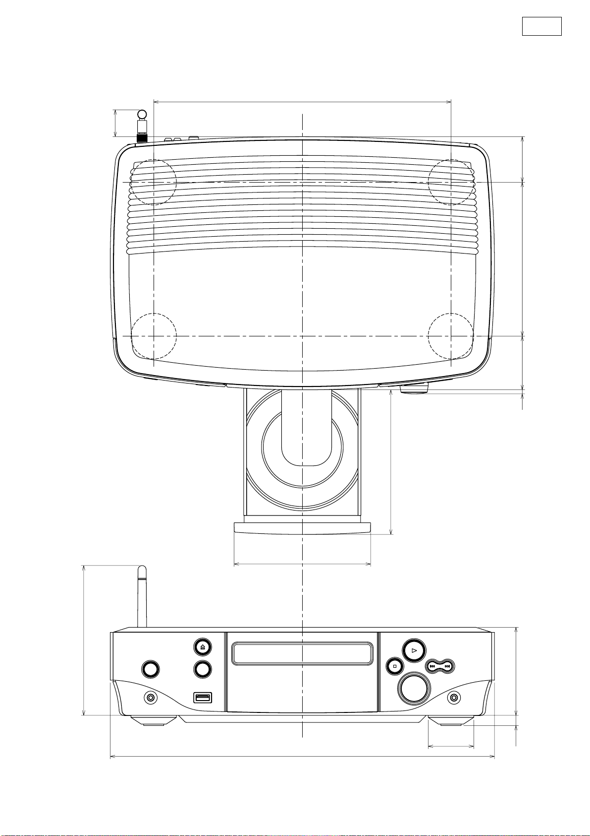
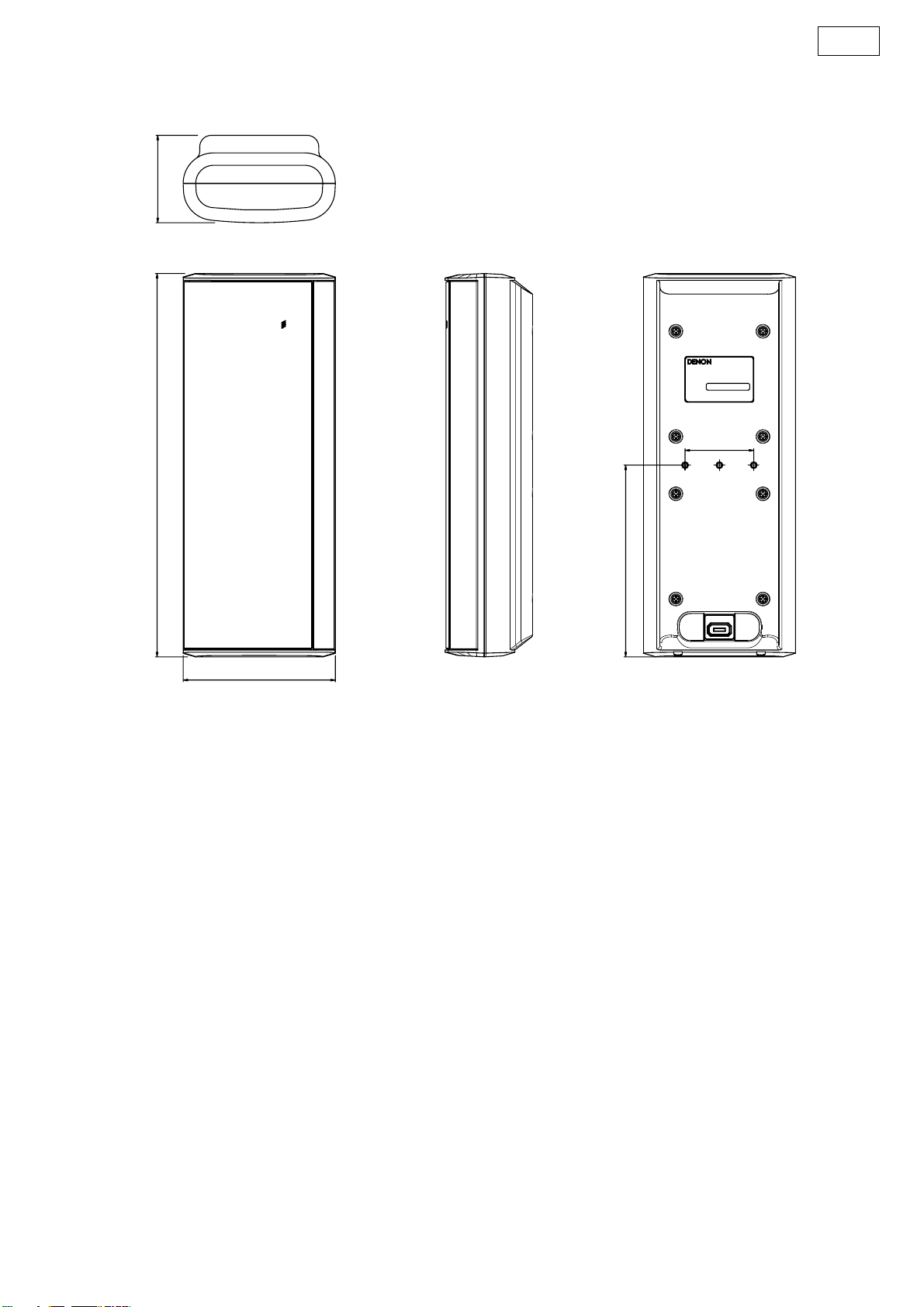
DIMENSION
ADV-S302
㪉㪍㪅㪌
㩿㪮㫀㪽㫀㩷㪘㪥㪫㪜㪥㪥㪘㪀
S-302
㪉㪐㪋
㪈㪋㪏
㩿㪮㫀㪽㫀㩷㪘㪥㪫㪜㪥㪥㪘㪀
㪋 㪌㪊 㪈㪌㪉 㪋㪌
㪈㪋㪉㪅㪏
㪈㪊㪌
㪏㪎㪈㪇
㪊㪏㪇
㪋㪌
3
Page 4
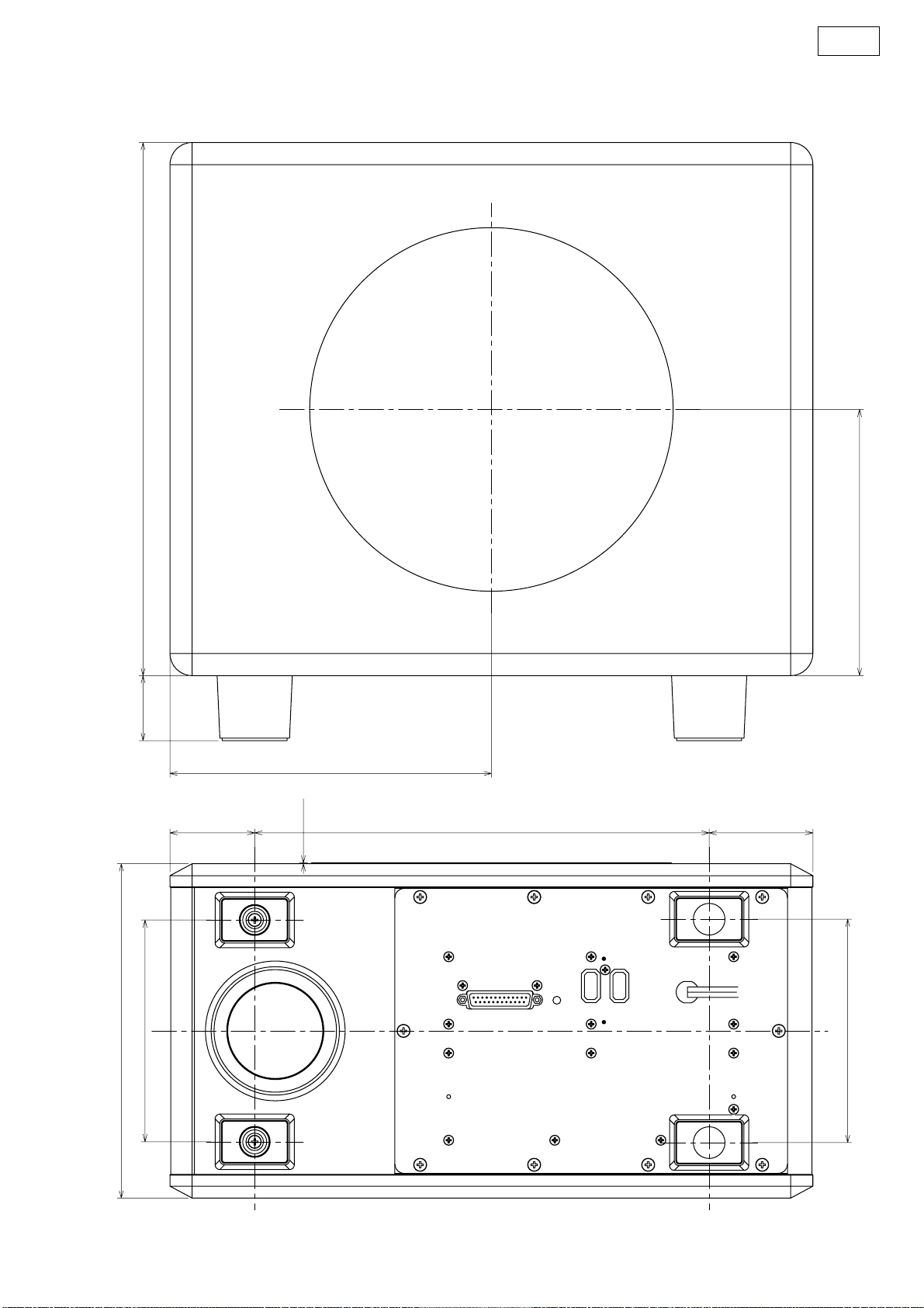
DSW-S302
㪊㪊㪍㪅㪌
S-302
㪋㪈
㪇㪅㪌
㪈㪍㪏
㪉㪇㪊
㪍㪌㪅㪌㪉㪏㪎㪌㪊㪅㪌
㪉㪈㪈
㪈㪋㪇
㪈㪋㪈
4
Page 5
SC-S302
S-302
76.3
60
335
133
167.5
5
Page 6
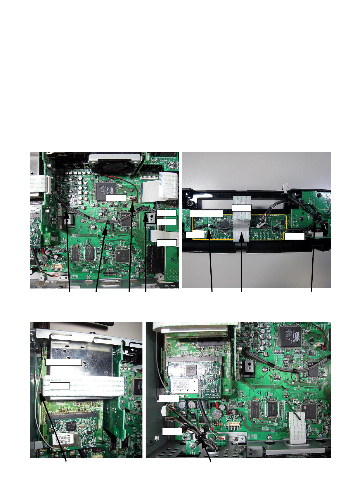
S-302
WIRE ARRANGEMENT
If wire bundles are untied or moved to perform adjustment or
parts replacement etc., be sure to rearrange them neatly as
they were originally bundled or placed afterward.
Otherwise, incorrect arrangement can be a cause of noise
generation.
1. ADV-S302
① Fasten the CX31 3P connector cord to the circuit board with
a style pin.
② Fasten the CX33 3P connector cord and CY072 7P connec-
tor cord to the circuit board with a style pin and clamp band.
③ Pass the CY211 FFC through the protect sheet.
④ Pass the CW052 5P connector cord through the protect
sheet.
⑤ Fasten the CW051 5P connector cord and CW052 5P
connector cord to the circuit board with a cord holder.
CX031
ワイヤー整形図
調整や部品の交換等により、ワイヤー類の結束をはずしたり移
動させた場合には、それらの作業が完了した時点でワイヤーの
整形をおこなってください。正しく整形されてないとノイズ発
生の原因となることがあります。
1. ADV-S302
① CX031 3P コネクターコードをスタイルピンで基板に固定
する。
② CY033 3P コネクターコードとCY0727P コネクターコー
ドをスタイルピンとクランプバンドで基板に固定する。
③CY211 のFFCをProtectSheetに通す。
④ CW052 5P コネクターコードを ProtectSheet に通す。
⑤ CW051 5P コネクターコードとCW0525P コネクターコー
ドをコードホルダーで基板に固定する。
CY072
CY033
CX171
①⑤④③②② ②
⑥ Pass the antenna cable next to the CX154 FFC.
⑦ Fasten the CW051 5P connector cord and CW052 5P
connector cord with a cord holder.
Anntena Cable
Protect Sheet
CW052
⑥ AnntenaCableは CX154の FFC の横を通す。
⑦ CW051 5P コネクターコードとCW0525P コネクターコー
ドをコードホルダーで固定する。
CY211
CW051
CX154
CW052
CW051
⑦⑥
6
Page 7
S-302
⑧ Fasten the CX061 6P connector cord with a cord holder.
CX061
Ferrite Cramp
⑧ CX061 6P コネクターコードをコードホルダーで固定す
る。
⑧⑧
7
Page 8
S-302
2. DSW-302
① Fasten the CX041 4P connector cord to the chassis with a
clamp band.
② Fasten the CW041 4P connector cord and CX081 8P con-
nector cord to the chassis with a clamp band.
③ Fasten with a clamp band.
④ Fasten the CX021 2P connector cord to the chassis with a
clamp band.
CX151
CX041 CX081
2. DSW-302
① CX041 4P コネクターコードをクランプバンドでシャーシ
に固定。
② CW041 4P コネクターコードと CX0818P コネクターコー
ドをクランプバンドでシャーシに固定。
③ クランプバンドで結束。
④ CX021 2P コネクターコードをクランプバンドでシャーシ
に固定。
④
CX021
③
CX022
①②
8
Page 9
S-302
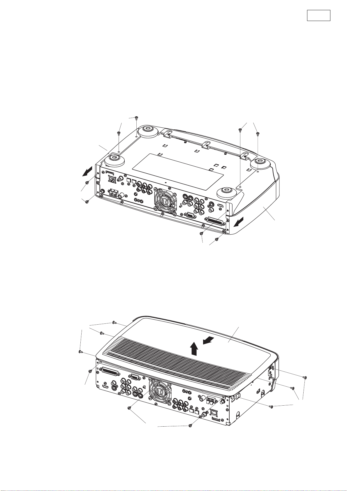
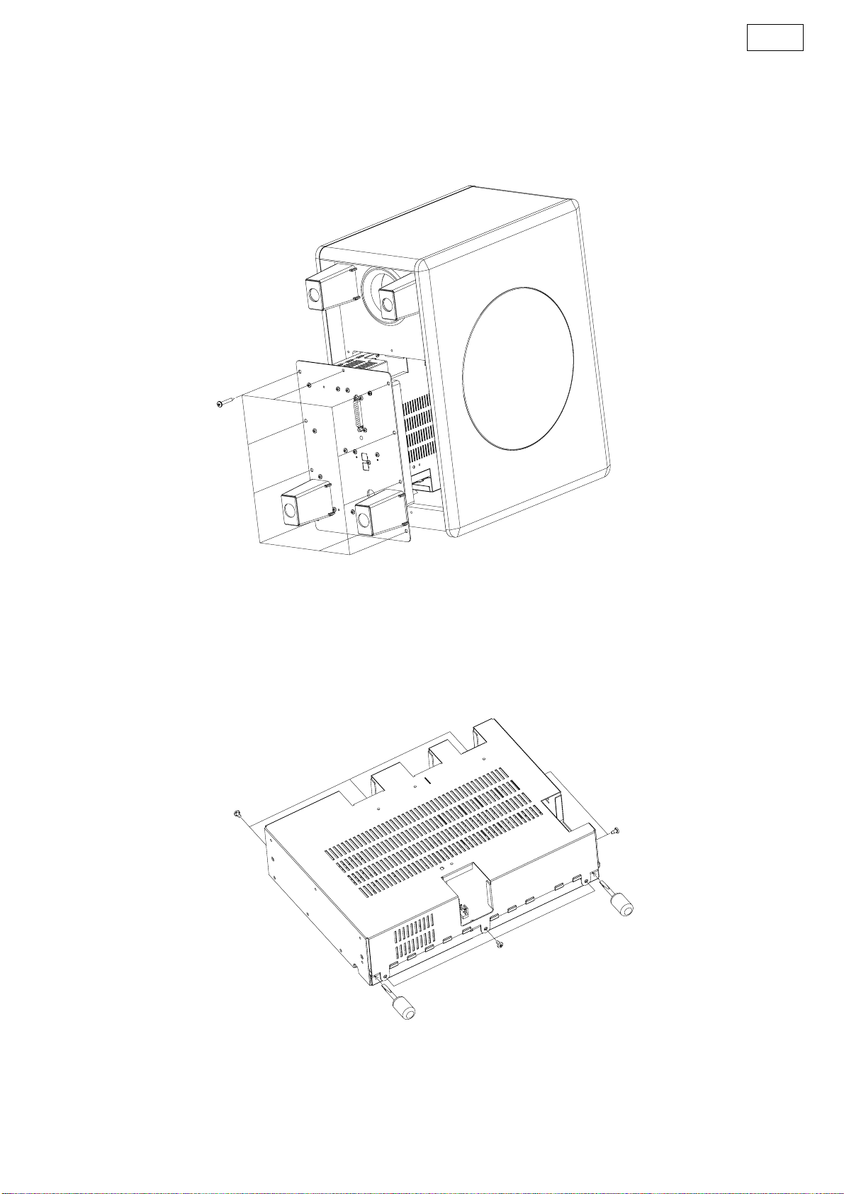
DISASSEMBLY
(Follow the procedure below in reverse order when reassembling.)
● ADV-S302
1. Side panel
(1) Remove 4 screws 104 on the rear side and 4 screws 104
on the bottom side.
(2) Detach the Side panel.
104
Side panel
104
各部のはずしかた
(組み立てるときは、逆の順序でおこなってください。)
● ADV-S302
1. Sidepanel
(1) 背面側から 104 のねじ 4 本と底面側から 104 のねじ 4
本をはずします。
(2) Sidepanelをはずします。
104
2. Top cover
(1) Remove 3 screws 104 on the rear side and 6 screws 105
on the both sides.
(2) Detach the Top cover.
105
104
Side panel
104
2. Topcover
(1) 背面側から 104 のねじ 3 本と側面側から 105 のねじ 6
本をはずします。
(2) Topcover をはずします。
Top cover
104
105
9
Page 10
S-302
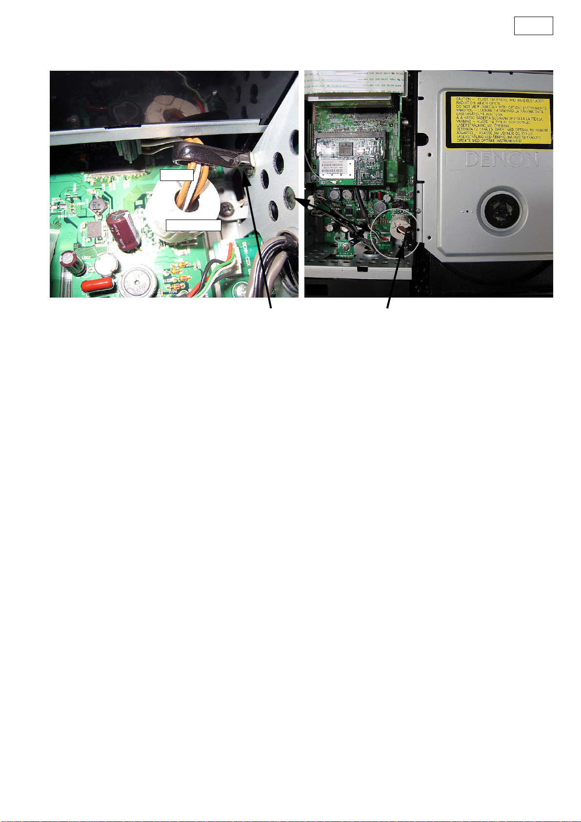
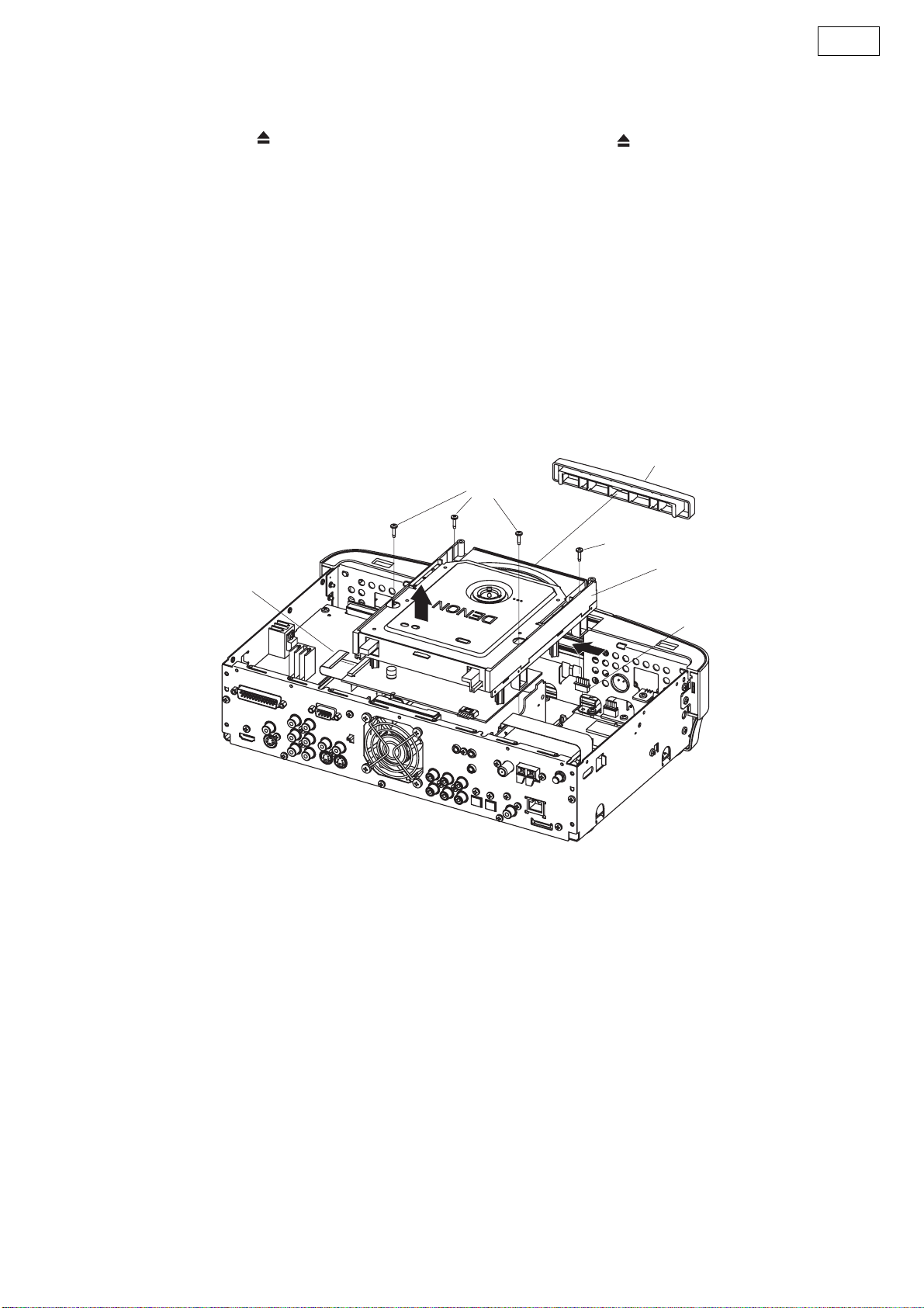
3. Drive unit
3.1. When the Disc tray can be ejected electrically.
(1) Switch on, and press [ (OPEN/CLOSE)] button to open
the Disc tray.
(2) Detach the Loader panel by lifting.
(3) Close the Disc tray.
(4) Remove 4 screws 102 on the top side.
(5) Disconnect the Wire [CX061] from the Main unit and the
FFC cable [CY301] from the Drive unit.
(6) Detach the Drive unit
3.2. When the Disc tray cannot be ejected
electrically.
(1) Push the Plate Gear of the Drive unit from direction of
arrow A, to open the Disc Tray.
(2) The same steps described on 3.1. (2)~(6).
3. Driveunit
3.1. ディスクトレイが電源でオープン出来る場合
(1) 電源を入れ「 (OPEN/CLOSE)」ボタンを押して、ディ
スクトレイを開きます。
(2) LoaderPanel を持ち上げてはずします。
(3) ディスクトレイを閉じます。
(4) 天面側から 102 のねじ 4 本をはずします。
(5) Mainunit からワイヤー [CX061]と Driveunit から FFC
ケーブル [CY301] をはずします。
(6) Driveunit をはずします。
3.2. ディスクトレイが電源でオープン出来ない場合
(1) 矢印 A 方向から Driveunit のプレートギアを押して
ディスクトレイを開きます。
(2) 3.1.(2) 〜 (6) の作業に同じ。
Loader panel
102
FFC Cable
102
Drive unit
Wire
A
10
Page 11
S-302
4. Front panel assy
(1) Remove 3 screws 106 on the bottom side.
(2) Disconnect the Wire [CX051],[CX052] and the FFC cable
[CX211] from the Main unit and the Wire [CX054] from
the USB unit.
(3) Remove 3 screws 103 and 2 screws 105 on the top side
and 2 screws 105 on the both sides.
(4) Detach the Front panel assy.
4. Frontpanelassy
(1) 底面側から 106 のねじ 3 本をはずします。
(2) Mainunit からワイヤー [CX051]、[CX052] と FFC ケー
ブル [CX211] を USB キバンからワイヤー [CY054] をは
ずします。
(3) 天面側から 103 のねじ 3 本と 105 のねじ 2 本を側面側
から 105 のねじ 2 本をはずします。
(4) Frontpanelassy をはずします。
106
Front panel assy
Front panel assy
105
103
FFC Cable
105
Wire
103
105
105
Wire
11
Page 12
S-302
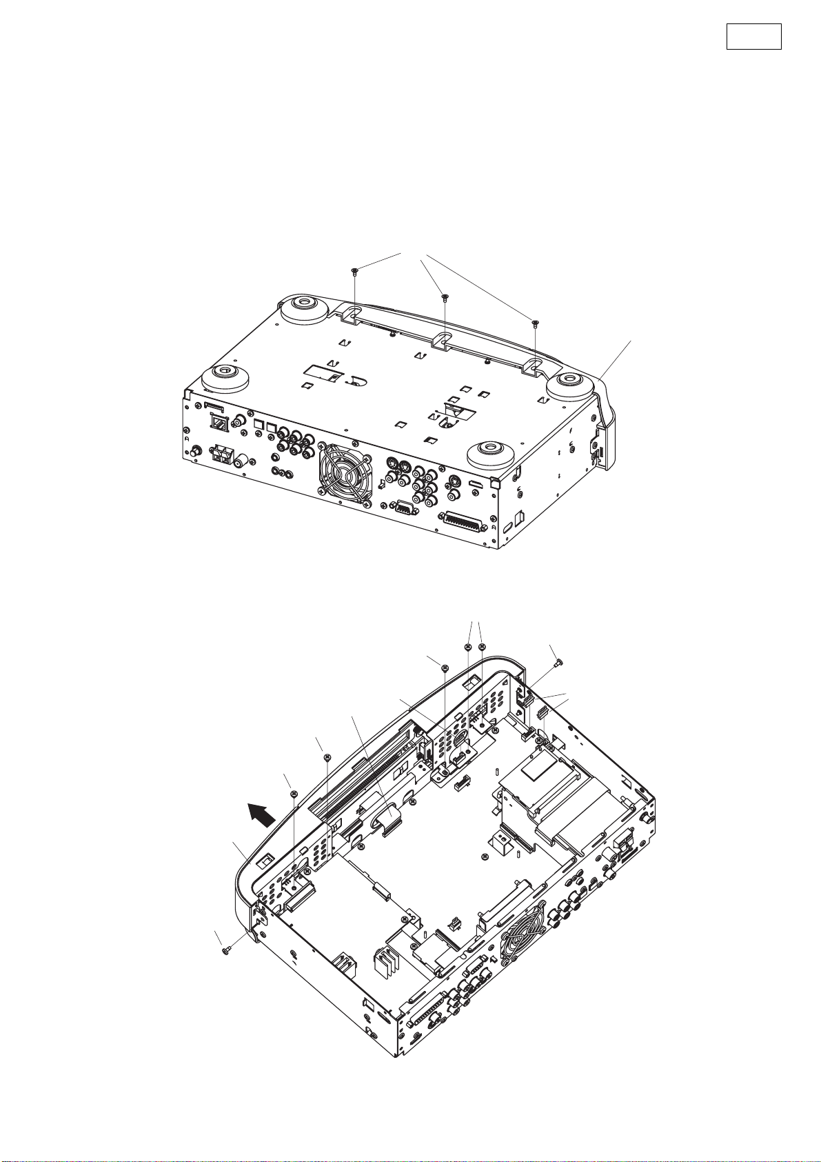
5. Rear panel assy
(1) Remove 10 screws 103 on the top side.
(2) Remove 5 screws 105 on the rear side and 4 screws 105
on the both sides.
(3) Detach the Rear panel assy.
103
103
5. Rearpanelassy
(1) 天面側から 103 のねじ 10 本をはずします。
(2) 後面側から 105 のねじ 5 本を側面側から 105 のねじ 4
本をはずします。
(3) Rearpanelassy をはずします。
Rear panel assy
103
105
105
103
103
105
Rear panel assy
105
12
Page 13
S-302
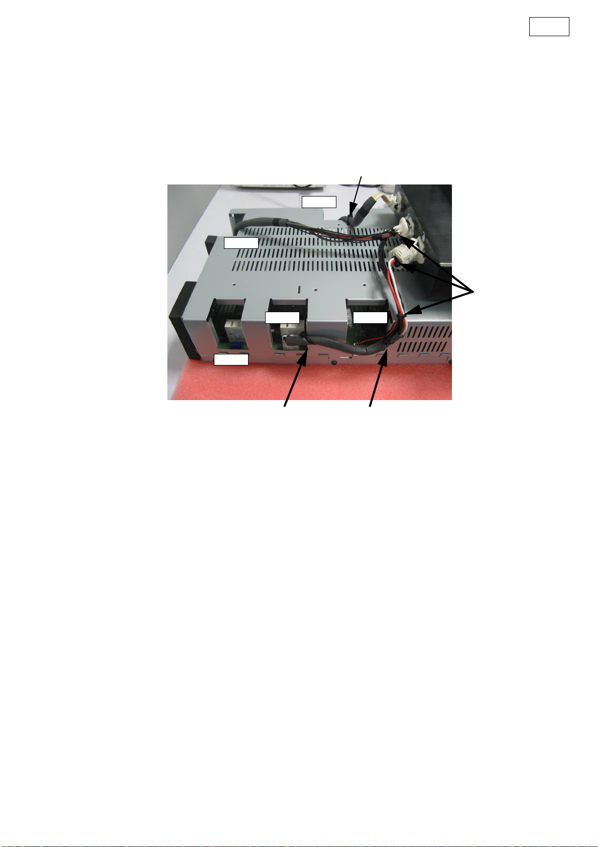
● DSW-S302
1. Rear panel
(1) Remove 10 screws 101 on the bottom side.
(2) Detach the Rear panel.
101
● DSW-S302
1. Rearpanel
(1) 底面側から 101 のねじ 10 本をはずします。
(2) Rearpanelをはずします。
2. SHIELD COVER
(1) Remove 8 screws 103 on the Side.
(2) Lift the shield cover using a flat-headed screwdriver and
remove it. When doing this, be careful not to deform the
main bracket's hook.
103
2. SHIELDCOVER
(1) 側面側から 103 のねじ 8 本をはずします。
(2) マイナスドライバーでシールドカバーを持ち上げては
ずします。このとき、メインブラケットのつめを変形
させないように注意してください。
103
103
13
Page 14
S-302
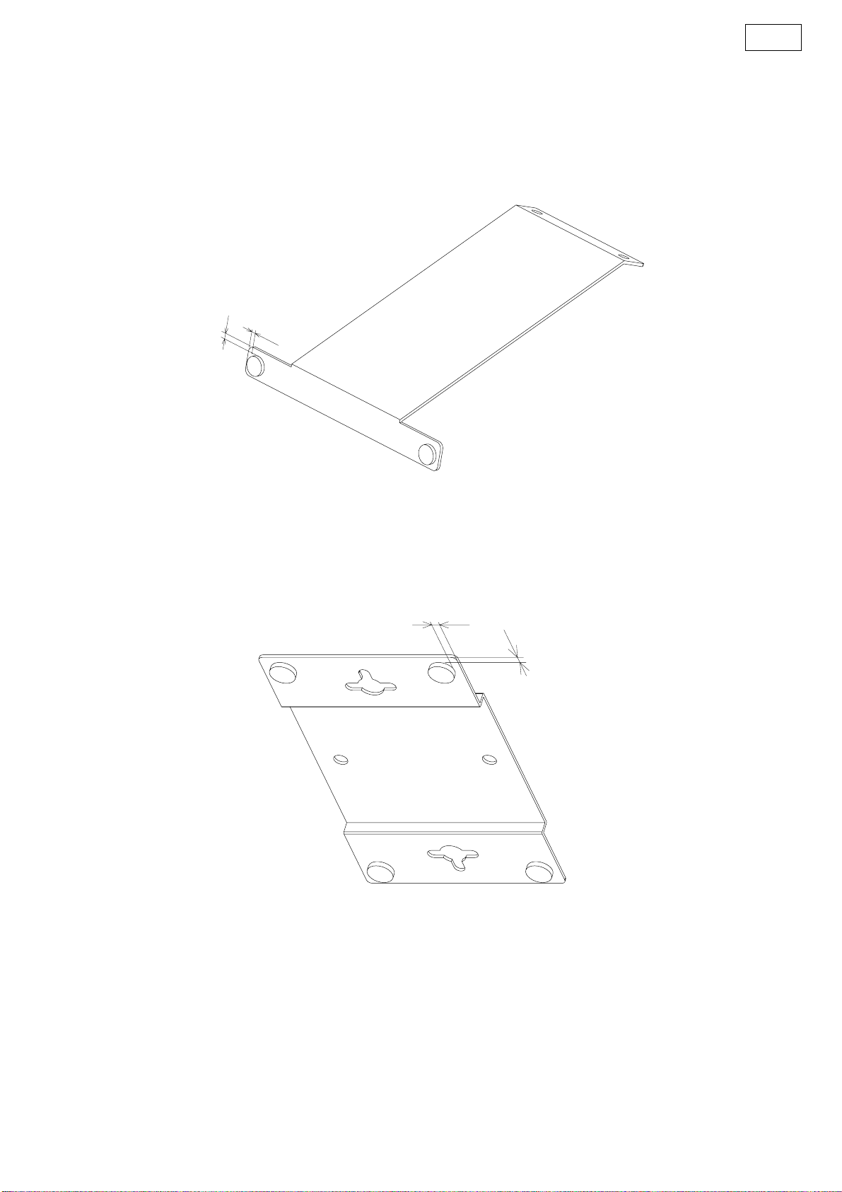
ATTACHING THE ANTI-SLIP PADS
※ Attach the anti-slip pads as shown on the diagram below.
Press firmly so they do not peel off subsequently.
● Speaker stand
2mm
2mm
すべり止めの貼りかた
※ 下図のように、すべり止めを貼り付けます。
後から剥がれないよう、充分に押し付けてください。
● スピーカースタンド
● Wall bracket
● 壁掛けブラケット
3mm
3mm
14
Page 15
S-302
DIAGNOSTICS OF OPTICAL PICKUP AND REPLACING TRAVERSE UNIT
Make failure diagnostics of the Optical Pickup as follows.
If the laser drive current (Iop) becomes more than 1.5 times of
the initial value, the Optical Pickup should be replaced.
The laser drive current initial value is checked by "Iop checked
Method" of next page.
In case of replacing the Pickup, change the whole part of the
Traverse Unit.
No mechanical adjustment is necessary after the replacement.
レーザー駆動電流初期値 :
Laser drive current initial value:
DVD:
CD:
FLDisplay(Thedisplaypartof13digits)
12345678910111213
T22―mmmm―nnnn
FLDisplay(Thedisplaypartof13digits)
12345678910111213
T2 1 ―mmmm―nnnn
光ピックアップの故障診断とトラバース
ユニットの交換
次の順序で故障診断を行ってください。
レーザー駆動電流 Iop 値が初期値の 1.5 倍以上になっている
場合は光ピックアップ交換の目安となります。
レーザー駆動電流初期値は、次ページ "Iop 値の確認方法 " で
確認できます。
ピックアップ交換の場合は、トラバースユニット単位での交
換となります。メカの調整は不要です。
Disc no read, unsteady playback, etc.
Laser drive current (Iop) check
HF wave form check
(Refer to WAVE FORMS)
Present value exceeds the initial value by 1.5 times
Traverse Unit replacing
ディスクを読み込まない
スムーズに再生しない、等
レーザー駆動電流 Iop 値の確認
HF 波形の確認
(WAVEFORMS参照)
現在値が初期値の
1.5 倍になっている
トラバースユニット交換
Laser current (Iop) memorizing after replacement
交換後にレーザー電流値の記憶
15
Page 16
S-302
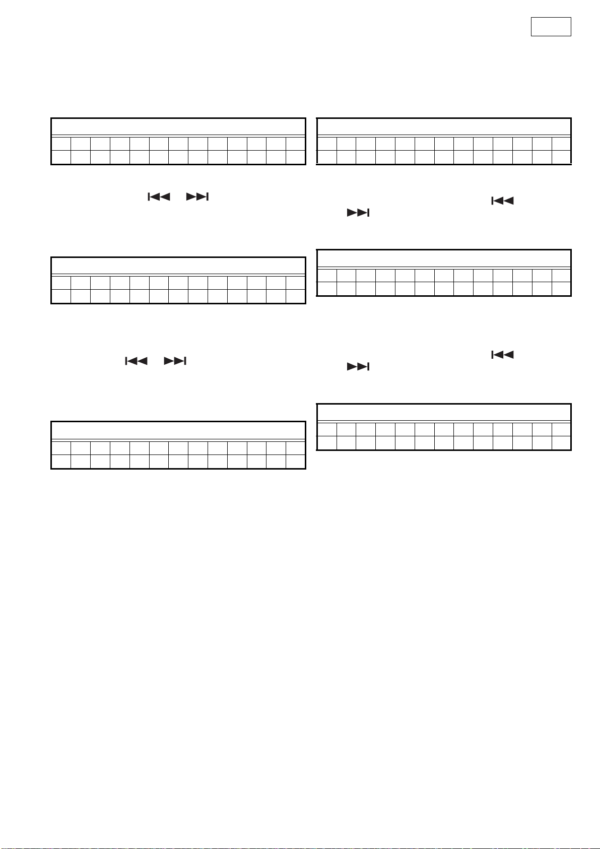
1. Iop checked Method
Select the laser ON/OFF (CD/DVD) mode of the test mode,
and check the lop value of DVD laser or CD laser.
(See page 21 for test mode.)
FLDisplay(Thedisplaypartof13digits)
12345678910111213
T2 L a s e r O n O f f
1.1. DVD laser current check
(1) Press the SKIP or button to display the la-
ser current value, and then select T22.
(2) Press the PLAY button and check the current value of
Iop (nnnn).
(Use the disc TDV-520)
FLDisplay(Thedisplaypartof13digits)
12345678910111213
T22―mmmm―nnnn
( − : Off, DVD laser, Initial value: mm.mm [mA],
Current value: nn.nn [mA])
1.2. CD Laser current check
(1) Press the or button to display the laser
current value, and then select T21.
(2) Press the PLAY button and check the current value of
Iop (nnnn).
(Use the disc TCD-784)
FLDisplay(Thedisplaypartof13digits)
12345678910111213
T2 1 ―mmmm―nnnn
( − : Off, CD laser, Initial value: mm.mm [mA],
Current value: nn.nn [mA])
d
d
1. Iop 値の確認方法
レーザー駆動電流を確認する場合は、テストモードのレー
ザー ON/OFF(CD/DVD) モードを選択して、DVD レーザー
または CD レーザーの lop 値を確認します。
(詳細は 21 ページ、テストモード参照)
FL 管の表示 (13 桁の表示部 )
12345678910111213
T2 L a s e r O n O f f
1.1. DVD レーザー電流確認
(1) レーザー電流値を表示する場合は、 ボタンまたは
ボタンを押し、T22 を選択します。
(2) PLAYボタンを押して、現在のlop値(nnnn)を確認します。
(Disc は TDV-520 を使用 )
FL 管の表示 (13 桁の表示部 )
12345678910111213
T22―mmmm―nnnn
( −:消灯、DVD レーザー、初期値:mm.mm[mA],
現在値:nn.nn[mA])
1.2. CD レーザー電流確認
(1) レーザー電流値を表示する場合は、 ボタンまたは
ボタンを押し、T21 を選択します。
(2) PLAYボタンを押して、現在のlop値(nnnn)を確認します。
(Disc は TCD-784 を使用 )
FL 管の表示 (13 桁の表示部 )
12345678910111213
T2 1 ―mmmm―nnnn
( −:消灯、CD レーザー、初期値:mm.mm[mA],
現在値:nn.nn[mA])
d
d
2. Note for Handling the Laser Pick-Up
The protection for the damage of laser diode.
If you want to change the optical device unit from any other
units, you must keep the following.
(1) It should be done at the desk already took measures the
static electricity in care of removing the OPU's (Optical
device unit) connector cable.
(2) Workers should be put on the "Earth Band".
(3) It should be done to add the solder to the short land to
prevent the broken Laser diode before removing the 24P
FFC cable.
(4) Don't touch OPU's connector parts carelessly.
3. Replacement of the Laser Pick-up
(Traverse Unit)
Check the Iop (Laser drive current)
If the present Iop (current) value exceeds.+150% of the initial value, replace the Traverse unit (Laser Pick-up) with a
new one.
2. レーザーピックアップの取扱注意
レーザーダイオードの破壊防止。
光素子ユニットを交換するときは、以下を遵守してくださ
い。
(1) 光素子ユニットの接続ケーブルをはずすときは、静電対
策を行ったデスク上で作業してください。
(2) 作業者は、リストストラップを使用してください。
(3) レーザーダイオードの破壊防止のため、24PFFC ケーブ
ルをはずす前にランドを半田付けショートしてくださ
い。
(4) 光素子ユニットのコネクタ部に触れないでください。
3. レーザーピックアップ ( トラバースユニッ
ト ) の交換
Iop( レーザー駆動電流)をチェックします。
現在の Iop 値が初期値の 150%を越えている場合、トラバー
スユニット(レーザーピックアップ)を交換してください。
16
Page 17
S-302
4. Rewriting the default value of the laser
current
To rewrite the default value of the laser current, press the
button for at least 5 seconds while the CD or DVD laser
current is displayed, then press the or button
to select T23. (For details, see "Iop checked Method" on
page 22.)
If the button is pressed while T23 is displayed, the current value is displayed at "mmmm" and stored in the EEPROM.
FLDisplay(Thedisplaypartof13digits)
12345678910111213
T23 ―mmmm―――――
5. Resetting the accumulated laser on time
To clear the accumulated laser on time, press the button
while the accumulated laser on time is displayed (TB1, TB2
: For details, see "Test Mode" on page 22.) until " * " appears at the fourth position, then press the or
button to select TB3.
If the button is pressed while TB3 is displayed, the accumulated laser on time of CD and DVD is cleared.
When TB1 or TB2 is selected with the or button, "nnnnnnn" is displayed as 0 so you can check.
FLDisplay(Thedisplaypartof13digits)
12345678910111213
TBY―――nnnnnnn
( − : Off, Y:1: CD, 2: DVD, nnnnnnn: Hour [h])
4. レーザー電流初期値の書き換え方法
レーザー電流の初期値を書き換えるには、CD または DVD
レーザー電流が表示されている時に ボタンを5秒以上押
し、次に ボタンまたは ボタンを押して T23 を
選択します。(詳細は 22 ページ、Iop 値の確認方法参照)
T23 表示時に ボタンを押と、mmmm 部に現在値を表示
し、EEPROM に保存します。
FL 管の表示 (13 桁の表示部 )
12345678910111213
T23 ―mmmm―――――
5. レーザー ON 累積時間のリセット方法
レーザーON 累積時間をクリアするには、レーザーON 累
積時間表示 (TB1,TB2) の時(詳細は 22 ページ、テストモー
ド参照)に ボタンを 4 桁目に ' * ' が表示されるまで押
し、 ボタンまたは ボタンを押し TB3 を表示させ
ます。
TB3 表示時に ボタンを押すと、CD 及び DVD レーザー
ON 累積時間をクリアします。
ボタンまたは ボタンで TB1 または TB2 を選択
すると、nnnnnnn 部が 0 表示となり確認できます。
FL 管の表示 (13 桁の表示部 )
12345678910111213
TBY―――nnnnnnn
( −:消灯、Y:1:CD,2:DVD、nnnnnnn:時間 [h])
17
Page 18
S-302
HOW TO REPLACE TRAVERSE UNIT
Caution: The optical pickup can be damaged easily by
static electricity charged on human body.
Take necessary anti-static measures when
repairing around the optical pickup.
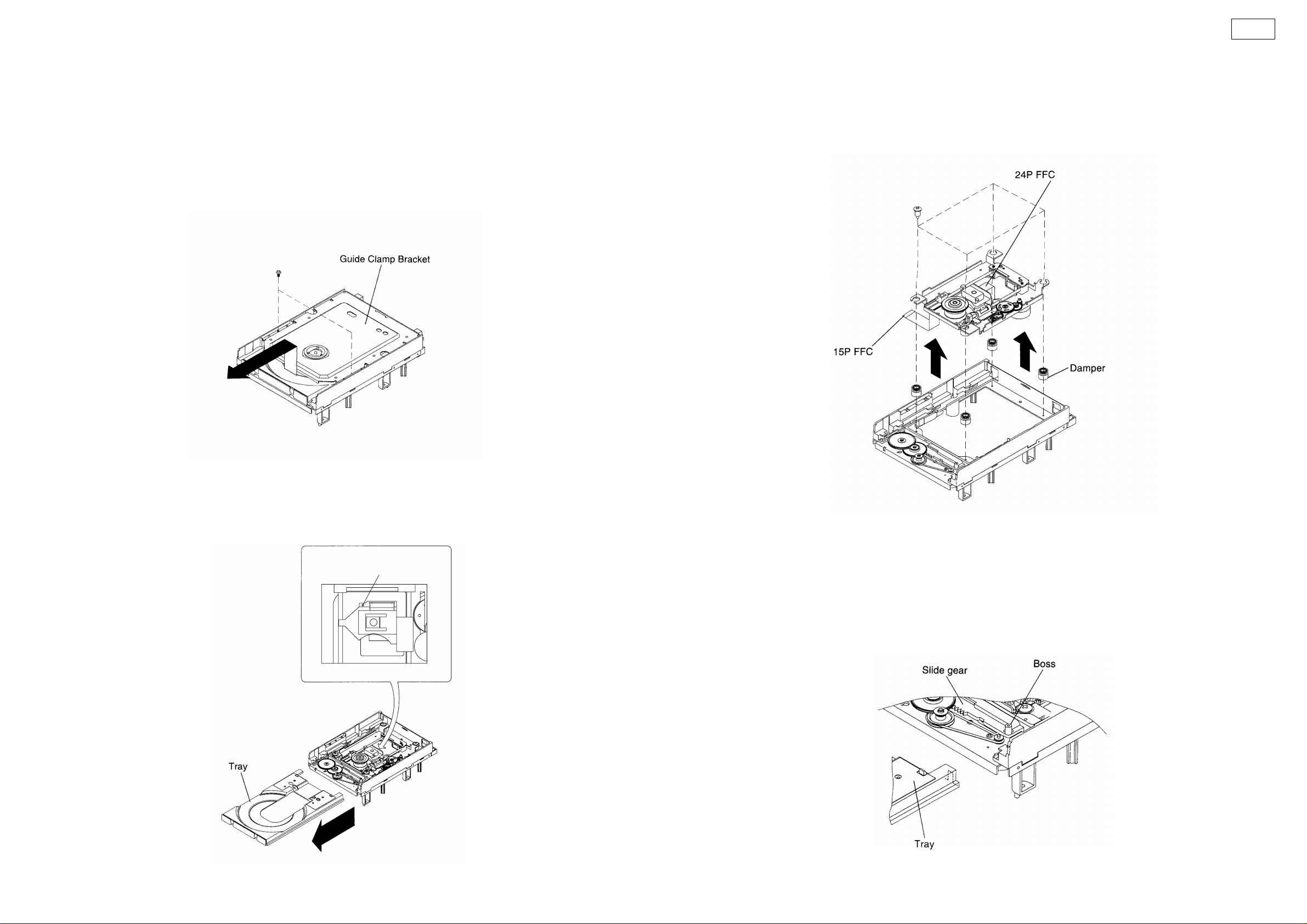
1. Guide Clamp Bracket disassembly
(1) Remove 2 screws.
(2) Remove Guide Clamp Bracket to arrow direction.
トラバースユニットの交換方法
注意 : 光ピックアップは、人体に帯電した静電気等で静電
破壊することがあります。光ピックアップ周辺を修
理する際は、必要な静電対策を行ってください。
1. ガイドクランプブラケットのはずしかた
(1) ねじ 2 本をはずします。
(2) ガイドクランプブラケットを矢印方向にとりはずしま
す。
3. Traverse Unit disassembly
(1) Remove 24P FFC, 15P FFC and 5P PH WIRE connect-
ing with from the Main P.W.B.
(2) Remove 4 screws fixing Damper.
(3) Remove Traverse Unit to arrow direction.
3. トラバースユニットのはずしかた
(1) メイン基板に接続している 24PFFC、15PFFC、5PPH
ワイヤをはずします。
(2) ダンパーを固定しているねじ 4 本をはずします。
(3) トラバースユニットを矢印方向にとりはずします。
2. Tray disassembly
(1) Remove to arrow direction.
(2) Solder the short-circuit (see in the frame).
2. トレイのはずしかた
(1) 矢印方向にとりはずします。
(2) 半田付けショートを行います。(枠内図参照 )
半田ショート
Solder to short-circuit
Short-circuit with Solder
半田ショート拡大図
Note for disassembly Traverse Unit
(1) When assembling, reverse the order of the above.
(2) When inserting Tray, confirm boss on Slide Cam set to
ditch of the Tray (Compare with below drawing).
トラバースユニット分解の注意
(1) 組み立てるときは、上記の逆の順序で行ってください。
(2) トレイ組込み時、スライドカムのボスがトレイの溝に
合っているか確認してください。(下図参照)
18
Page 19
S-302
SERVICE MODE
1. Aging Mode
1.1. preparation0
(1) Equipment used: Any one of DVD Karaoke Disc (containing more than 10 titles).
(ex : Heat run disc TDV-HR01)
(2) Unit setting : No spec other than the following procedure.
1.2. procedure
※ Perform aging of the DVD.
(1) Pressing the and buttons simultaneously, plug the AC cord into a power outlet. This sets the aging mode.
• Once the aging mode is set, press the FUNCTION button to switch the mode.
(After the display is put out at the switch, it selects.)
(a) To select the normal aging mode ... Start from (2)
(b) To select the error rate display mode ... Start from (8)
(2) Press the button and play all the tracks recorded on the disc.
(3) Both the " " and " " indicators light on the fluorescent display tube.
(4) When the button is pressed once with the tray open, titles 1 and 10 recorded on the disc are played.
(5) The " " indicator flashes and the " " indicator lights on the fluorescent display tube.
(6) Once playback is completed, open and close the tray and repeat the operation in step (3) or (4).
(7) If there is an error while in the aging mode, the error is displayed and the stop mode is set with the status at that time.
NOTE)・The FUNCTION button on the main unit and the FUNCTION selector button on the remote control unit will not work
during the aging mode.
・The ON/STANDBY buttons on the main unit and the remote control unit will not work during the aging mode.
(If the set's power is turned off, the DVD stops and the aging mode is canceled.)
サービスモードについて
1. エージングモード
1.1. 準備
(1) 使用機器:DVD カラオケディスク (10 タイトル以上のもの)
(例:ヒートランディスク TDV-HR01)
(2) 本体設定:下記設定以外規定無。
1.2. 手順
※ DVD のエージングをおこなう。
(1) 本体の ボタンと ボタンを同時に押しながら AC コードをコンセントへ接続すると、エージングモードが設定される。
・ エージングモード設定後、FUNCTION ボタンを押して、モードを切り替える。
(切り替え時に表示を出してから選択する。)
(a) 通常のエージングモードを選択・・・(2) から開始
(b) エラーレート表示モードを選択・・・(8) から開始
(2) ボタンを押し、ディスクに収録されている全ての曲を再生する。
(3) FL 管の インジケーターと インジケーターが両方とも点灯する。
(4) トレイを開いた状態で ボタンを 1 回押して、ディスクに収録されているタイトル 1 とタイトル 10 を再生する。
(5) FL 管の インジケーターが点滅し、 インジケーターが点灯する。
(6) 再生終了後、トレイを開閉させ (3) または (4) の動作をする。
(7) エージングモード中にエラーが発生すると、エラーを表示し、その時の状態で停止する。
注 )・ エージングモード中は、本体の FUNCTION ボタンおよび、リモコンの FUNCTION 切替ボタンは動作しない。
・ エージングモード中は本体およびリモコンの ON/STANDBY ボタンを動作しない。
(セットの電源を OFF にすると DVD が停止し、エージングモードが解除される。)
No. Error contents FL display
1 Bad DIsc
2 Forcus Error
3 Read Error
4 Tracking Error
5Tray Error
6 Navigation Pack Read Error
7 Cmmunication Error
FLDisplay(Thedisplaypartof13digits)
12345678910111213
E7 XX XX XX
No. エラー内容 FL 管表示
1 不良ディスク
2 フォーカスエラー
3 リードエラー
4 トラッキングエラー
5 トレイエラー
6 ナビゲーションパックエラー
7 コマンド通信エラー
FL 管の表示 (13 桁の表示部 )
12345678910111213
E7 XX XX XX
19
Page 20
S-302
2. Initial Setting Mode
2.1. Preparation
(1) Equipment used: None
(2) Unit setting: No spec other than the following procedure.
2.2. Procedure
● SYSTEM
※ This initializes the data for the function, volume, DVD mechanism, etc.
(1) When the ON/STANDBY button is pressed to turn the set on while pressing the main unit's FUNCTION and buttons
simultaneously, the initialization mode is set.
(2) The standby indicator lights yellow and "INITIALIZE" is displayed on the fluorescent display tube.
(If you set the button free, the LED indicator lights blue.)
(3) Once the entire initialization procedure has been completed, the set is in the normal mode with the power turned on.
d
● DVD
※ This initializes the data for the DVD mechanism.
(1) With the power on, set the function to DVD, and in the playback stopped mode, press the and buttons simultaneously
for at least 2 seconds to set the DVD initialization mode.
(2) "INITIALIZE" is displayed on the fluorescent display tube about 0.5 seconds.
d
3. µcom Firm Check Mode
3.1. Preparation
(1) Equipment used: None
(2) Unit setting: No spec other than the following procedure.
3.2. Procedure
※ Use this to display the version information, etc.
(1) When the STANDBY mode, the FUNCTION, the and the ON/STANDBY button are simultaneously pressed. Afterwards,
when the power supply of the set is turned on pressing the ON/STANDBY button, the system check mode is set.
(2) Press the STATUS button on the remote control unit to display the following information, in this order: System microprocessor
version → Date of system microprocessor version updating → ESS version → Date of ESS version updating → drive microprocessor version of DVD mechanism → M850 version → Region code.
(3) Unplug AC cord to clear this mode.
NOTE) The DVD mechanism driver version and ESS version are not displayed un less the function is once set to DVD.
2. イニシャルモード
2.1. 準備
(1) 使用機器:無
(2) 本体設定:下記手順以外規定無。
2.2. 手順
● システム
※ ファンクション、VOL 等および DVD メカのバックアップデータの初期化をおこなう。
(1) 本体 FUNCTION ボタンと ボタンを同時に押しながら、ON/STANDY ボタンを押してセットの電源を入れるとイニシャ
ルモードが設定される。
(2) スタンバイ LED が黄色に点灯し、FL 管にINITIALIZEが表示される。
( ボタンを離すと LED は青色点灯になる )
(3) 全ての初期化完了後、通常モードの電源 ON の状態になる。
d
●DVD
※ DVD のみのバックアップデータの初期化をおこなう。
(1) 電源 ON 時にファンクッションを DVD にし再生停止状態で、 ボタンと ボタンを 2 秒以上同時に押し続けると、
DVD 初期化モードが設定される。
(2) FL 管にINITIALIZEが 0.5 秒程表示される。
d
3. マイコンファームチェックモード
3.1. 準備
(1) 使用機器:無
(2) 本体設定:下記手順以外規定無。
3.2. 手順
※ バージョン表示等をおこなう。
(1) STANDBY 時に本体 FUNCTION ボタン、 ボタンと ON/STANDBY ボタンを同時に押す。その後、ON/STANDBY ボタンを
押してセットの電源を入れると、システムチェックモードが設定される。
(2) リモコンの STATUS ボタンを押すと、システムマイコンのバージョン→システムマイコンのバージョンアップ日→ ESS の
バージョン→ ESS のバージョンアップ日→ DVD メカのドライブマイコンのバージョン→ DM850 のバージョン→リージョ
ンコードの順に表示される。
(3) AC コードを抜くことにより、システムチェックモードを解除する。
注 ) DVD メカのドライブバージョン、ESS のバージョンの表示については、一度ファンクッションを DVD にしないと表示
されない。
20
Page 21
S-302
4. Test mode
4.1. Entering the test mode
To enter the test mode, press the and buttons simultaneously while in the Aging mode. Not insert the disc.
(The Aging mode is entered by pressing the and buttons simultaneously to turn on the AC power.
When the Aging mode is set, the and indicators light.)
Press and buttons simultaneously
Power turns on
Press and buttons simultaneously
Test mode
button
Set the disc
button
After the TOC reading
button
Aging mode
button
Set the disc
button
Aging mode start
4. テストモード
4.1. テストモードの設定
テストモードの設定はエージングモード時に ボタンと ボタンを同時に押すことでおこなう。ディスクは挿入していな
いこと。
( エージングモードの設定は ボタンと ボタンを同時に押しながら、AC コードをコンセントへ接続し、セットの電源を入れ
る。エージングモードになると FL 管の インジケーターと インジケーターが点灯する。)
ボタンと ボタンの同時押し
電源 ON
ボタンと ボタンの同時押し
テストモード
ボタン
ディスクを載せる
ボタン
TOC リード後
ボタン
エージングモード
ボタン
ディスクを載せる
ボタン
エージング開始
Test mode start
FL tube display when test mode entered
FLDisplay(Thedisplaypartof13digits)
12345678910111213
TEST MODE
4.2. Selecting the mode
The following modes are available.
(1) Laser on/off (CD/DVD) mode : T2
(2) Servo adjustment value display mode : T3
(3) Trace mode (error rate display) : T7
(4) Accumulated laser on time : TB
① When the button is pressed after entering the test mode, the display switches in the order: T2, T3, T7, TB, T2 …
FLDisplay(Thedisplaypartof13digits)
12345678910111213
T2 L a s e r O n O f f
FLDisplay(Thedisplaypartof13digits)
12345678910111213
T3 S e r v o A d j
テストモード開始
テストモード設定時の FL 管表示
FL 管の表示 (13 桁の表示部 )
12345678910111213
TEST MODE
4.2. モードの選択
モードには、次のモードがある。
(1) レーザー ON/OFF(CD/DVD) モード : T2
(2) サーボ調整値表示モード : T3
(3) トレースモード ( エラーレート表示 ) : T7
(4) レーザー ON 累積時間 : TB
①テストモード中に ボタンを押すと、T2,T3,T7,TB,T2…の順に表示される。
FL 管の表示 (13 桁の表示部 )
12345678910111213
T2 L a s e r O n O f f
FL 管の表示 (13 桁の表示部 )
12345678910111213
T3 S e r v o A d j
FLDisplay(Thedisplaypartof13digits)
12345678910111213
T7 T r a c e M o d e
FLDisplay(Thedisplaypartof13digits)
12345678910111213
TB L a s e r O n T i m
FL 管の表示 (13 桁の表示部 )
12345678910111213
T7 T r a c e M o d e
FL 管の表示 (13 桁の表示部 )
12345678910111213
TB L a s e r O n T i m
21
Page 22
S-302
4.3. Setting the mode
With the mode selected, press the button to set that mode.
① In the laser on/off (CD/DVD) mode, laser on/off control is executed and the laser current is displayed.
Press the or button to switch the CD/DVD (T21, T22, T21. .).
To save the current laser current value, press and hold in the button for at least 5 seconds to turn off the "mmmm" section
of the display, then press the or button and select T23. When the button is pressed while T23 is displayed, the
data is displayed in the "mmmm" section.
For the CD laser
FLDisplay(Thedisplaypartof13digits)
12345678910111213
T21―mmmm―nnnn
( − : Off, CD laser, Stored data: mm.mm [mA], Current value: nn.nn [mA])
For the DVD laser
FLDisplay(Thedisplaypartof13digits)
12345678910111213
T22―mmmm―nnnn
( − : Off, DVD laser, Stored data: mm.mm [mA], Current value: nn.nn [mA])
② In the servo adjustment value display mode (See "Table 1 - Servo adjustment value display mode details")
FLDisplay(Thedisplaypartof13digits)
12345678910111213
T X X −−−−−−nnnn
(XX : Selection mode, n : Adjustment value (HEX))
③ In the trace mode (error rate display), select the trace of the innermost circumference of 1 layer.
FLDisplay(Thedisplaypartof13digits)
12345678910111213
T71FFFFFFFFFF
(F : When address and error rate not set, F is displayed.)
④ Displaying the accumulated laser on time (stored in the EEPROM)
FLDisplay(Thedisplaypartof13digits)
12345678910111213
T B Y―――nnnnnnn
(Y : 1:CD, 2:DVD, nnnnn: Time [h])
※ Fractions of hours are counted up one hour on the display.
4.3. モードの確定
モードを選択してある状態で ボタンを押すとモードを確定する。
①レーザーON/OFF(CD/DVD) モードの場合、レーザーのON/OFF 制御を実行し、レーザー電流を表示する。CD/DVD の切り替
えは、 ボタンまたは ボタンを押す (T21、T22、T21..)。
現在のレーザー電流値を保存する場合、 ボタンを 5 秒以上押し続け、mmmm 部を非表示にし、 ボタンまたは
ボタンを押して、T23 を選択する。T23 を表示時に ボタンを押すと、mmmm 部にデータが表示される。
CD レーザーの場合
FL 管の表示 (13 桁の表示部 )
12345678910111213
T21―mmmm―nnnn
( −:消灯、CD レーザー、保存データ:mm.mm[mA],現在値:nn.nn[mA])
DVD レーザーの場合
FL 管の表示 (13 桁の表示部 )
12345678910111213
T22―mmmm―nnnn
( −:消灯、DVD レーザー、保存データ:mm.mm[mA],現在値:nn.nn[mA])
②サーボ調整値表示モードの場合 (表 1 サーボ調整値表示モード詳細参照)
FL 管の表示 (13 桁の表示部 )
12345678910111213
TXX――――――nnnn
(XX: 選択モード、n: 調整値 (HEX))
③トレースモード ( エラーレート表示 ) の場合は、1層内周のトレースを選択する。
FL 管の表示 (13 桁の表示部 )
12345678910111213
T71FFFFFFFFFF
(F: アドレス及びエラーレートは未確定時、F を表示する。)
④レーザー ON 累積時間 (EEPROM に記憶 ) を表示する。
FL 管の表示 (13 桁の表示部 )
12345678910111213
T B Y―――nnnnnnn
(Y:1:CD、2:DVD、nnnnn: 時間 [h])
※ 1 時間未満は切り上げて表示する。
22
Page 23
S-302
4.4. Change within the mode
Changes within modes are made by pressing the and buttons while the mode is set.
① In the laser on/off (CD/DVD) mode, laser on/off control is executed and the laser current is displayed.
For the CD laser
FLDisplay(Thedisplaypartof13digits)
12345678910111213
T21―mmmm―nnnn
( − : Off, CD laser, Stored data: mm.mm [mA], Current value: nn.nn [mA])
For the DVD laser
FLDisplay(Thedisplaypartof13digits)
12345678910111213
T22―mmmm―nnnn
( − : Off, DVD laser, mm.mm [mA], nn.nn [mA])
When there is no saved data (for the DVD laser)
FLDisplay(Thedisplaypartof13digits)
12345678910111213
T2 2 ――――――nnnn
( − : Off, DVD laser, nn.nn [mA])
To store the current value, press the button for " * " appears at the fourth position, then press the or button to
select T23.
If the button is pressed while T23 is displayed, the current value is displayed at "mmmm" and stored in the EEPROM.
FLDisplay(Thedisplaypartof13digits)
12345678910111213
T2 3 ―mmmm―nnnn
( − : Off, DVD laser, nn.nn [mA])
If the current value is over 100 mA, the 4th and 9th digit sections are used.
② In the servo adjustment value display mode (See "Table 1 - Servo adjustment value display mode details")
FLDisplay(Thedisplaypartof13digits)
12345678910111213
TXX――nnnnnnnn
(XX : Selection mode, n: Adjustment value (HEX))
For the adjustment values, 0's are added in front of the effective number of bytes.
(Ex.: If the value is 0x123 for 4-byte data, "00 00 01 23" is displayed.)
⑤ In the trace mode (error rate display) (See "Table 2 - Trace mode details")
FLDisplay(Thedisplaypartof13digits)
12345678910111213
TYYFFFFFFFFFF
(YY : Selection mode [71 to 94], F: When address and error rate not set, F is displayed.)
⑥ In the accumulated laser on time display
FLDisplay(Thedisplaypartof13digits)
12345678910111213
T B Y―――nnnnnnn
(Y : 1: CD, 2: DVD, nnnnnnn: Time [h]) ※ If the current value is over 100 mA, the 4th and 9th digit sections are used.
To clear the accumulated laser on time, press the button while the accumulated laser on time is displayed (TB1, TB2) until
" * " appears at the fourth position, then press the or button to select TB3.
If the PLAY button is pressed while TB3 is displayed, the accumulated laser on time of CD and DVD is cleared.
When TB1 or TB2 is selected with the or button, "nnnnnnn" is displayed as 0 so you can check.
4.4. モード内での変更
モードを確定してある状態で ボタンまたは ボタンを押すとモード内での変更をおこなう。
①レーザーON/OFF(CD/DVD) モードの場合、レーザーのON/OFF 制御を実行し、レーザー電流を表示する。
CD レーザーの場合
FL 管の表示 (13 桁の表示部 )
12345678910111213
T21―mmmm―nnnn
( −:消灯、CD レーザー、保存データ:mm.mm[mA],現在値:nn.nn[mA])
DVD レーザーの場合
FL 管の表示 (13 桁の表示部 )
12345678910111213
T22―mmmm―nnnn
( −:消灯、DVD レーザー、mm.mm[mA],nn.nn[mA])
保存データなしの場合 (DVD レーザーの場合 )
FL 管の表示 (13 桁の表示部 )
12345678910111213
T22――――――nnnn
( −:消灯、DVD レーザー、nn.nn[mA])
現在値を保存するには、 ボタンを 4 桁目に*が表示されるまで押し、次に ボタンまたは ボタンを押して T23
を選択する。T23 表示時に、 ボタンを押すと、mmmm 部に現在値を表示し、EEPROM に保存される。
FL 管の表示 (13 桁の表示部 )
12345678910111213
T2 3 ―mmmm―――――
( −:消灯、DVD レーザー、mm.mm[mA])
電流値が 100mA 以上の場合は、4 桁、9 桁部分を使用。
②サーボ調整値表示モードの場合 (表 1 サーボ調整値表示モード詳細参照)
FL 管の表示 (13 桁の表示部 )
12345678910111213
TXX――nnnnnnnn
(XX: 選択モード、n: 調整値 (HEX))
調整値は、有効バイト数分先頭に 0 をつける。
(例:4 バイトデータで値が 0x123 の場合は00000123)
③トレースモード ( エラーレート表示 ) の場合(表 2 トレースモード詳細参照)
FL 管の表示 (13 桁の表示部 )
12345678910111213
TYYFFFFFFFFFF
(YY: 選択モード [71 〜 94]、F: アドレス及びエラーレートは未確定時、F を表示する。)
⑥レーザー ON 累積時間を表示場合
FL 管の表示 (13 桁の表示部 )
12345678910111213
T B Y―――nnnnnnn
(Y:1:CD,2:DVD、nnnnnn: 時間 [h]) ※ 1 時間未満は切り上げて表示する。
レーザー ON 累積時間をクリアする場合、レーザー ON 累積時間表示時 (TB1、TB2) のとき、 ボタンを 4 桁目に*が表
示されるまで押し、 ボタンまたは ボタンを押し、TB3 を表示させる。TB3 表示時に ボタンを押すと CD および
DVD レーザー ON 累積時間をクリアする。 ボタンまたは ボタンを押して、TB1 または TB2 を選択すると、
nnnnnn 部が 0 表示になり確認できる。
23
Page 24
S-302
4.5. Execution of trace mode (error rate display) (See "Table 2 - Trace mode details")
Trace will be performed if the button is pushed after choosing operation.
FLDisplay(Thedisplaypartof13digits)
12345678910111213
TYYmmmmmmllll
(YY : selection mode [71 to 94], m : address [PBA][HEX], l : error rate [COUNT/SEC] [HEX])
Note) CD : Error rate of 75 frames is displayed (1 second).
DVD : Error rate of 8ECC block is displayed.
The mode chosen when selection mode was changed into the trace execution and the button was pushed is performed
from the beginning.
When the button is pushed without changing selection mode, the mode under selection is performed from the beginning.
(If the button is pushed, the address corresponding to the chosen mode will be searched again.)
The pause mode is set after tracing is completed.
4.6. Other operations
① When the button is pressed, the mode returns to the previously selected mode.
4.5. トレースモード ( エラーレート表示 ) の実行(表 2 トレースモード詳細参照)
動作を選択した後、 ボタンを押すとトレースを実行する。
FL 管の表示 (13 桁の表示部 )
12345678910111213
TYYmmmmmmllll
(YY: 選択モード [71 〜 94]、m: アドレス [PBA][HEX]、l: エラーレート [COUNT][DEC])
注 ) CD : 表示するエラーレートは、75 フレーム分の値 (1 秒 )。
DVD : 表示するエラーレートは、8ECC ブロック分の値。
トレース実行中に選択モードを変更し、 ボタンを押すと選択したモードを最初から実行する。
選択モードを変更せずに ボタンを押した場合も、選択中のモードを最初から実行する。
( ボタンを押すと、選択しているモードに対応したアドレスを再度サーチする。)
トレース終了時は、PAUSE 状態になります。
4.6. その他の動作
① ボタンを押すと、前の選択モードに戻る。
(1) Test mode detailed table
Table 1: Servo adjustment value display mode details
XXX
Name Size Meaning Remarks
T31 fbal0 16bits CD/DVD L0 layer focus balance adjust-
T32 tbal0 16bits CD/DVD L0 layer tracking balance adjust-
T33 fcga0 16bits CD/DVD L0 layer focus Loop Gain adjust-
T34 tkga0 16bits CD/DVD L0 layer tracking Loop Gain
T35 Fbal1 16bits DVD L1 layer focus balance adjustment
T36 Tbal1 16bits DVD L1 layer tracking balance adjustment
T37 Fcga1 16bits DVD L1 layer focus Loop Gain adjustment
T38 Tkga1 16bits DVD L1 layer tracking Loop Gain adjust-
T39 Asoffs 16bits AS signal Offset value Upper 10 bit is valid
T40 Envoffse 16bits ENV signal Offset adjustment value Upper 10 bit is valid
T41 Foffse 16bits FE signal Offset adjustment value Upper 10 bit is valid
T42 Teoffse 16bits TE signal Offset adjustment value Upper 10 bit is valid
T43 RFfc 8bits RF signal frequency adjustment value
T44 RFbst 8bits RF signal Boost adjustment value
T45 RFgdl 8bits
T46 RFgdh 8bits
ment value
ment value
ment value
adjustment value
value
value
value
ment value
RF signal low range group delay adjust-
ment value
RF signal high range group delay adjust-
ment value
FBAL range: 0x8000 < FBAL < 0x7FC0(Center:0x0000)
TBAL range: 0x0000 < TBAL < 0x003F
1x for 0x100 [0x200 (2x) set to Typ.
(1x for 0x100, 2x for 0x200. Y/0x100 ratio calculation.)
Adjustment value 0x200 sets so that gain crossover reaches target.
1x for 0x100 [0x200 (2x) set to Typ.
(1x for 0x100, 2x for 0x200. Y/0x100 ratio calculation.)
Adjustment value 0x202 sets so that gain crossover reaches target.
Adjustment range : 0x0000 〜 0x001F
0x0000 : 0dB
0x001F : 14dB
(1) テストモード詳細一覧表
表 1サーボ調整値表示モード詳細
XXX 名称 サイズ 意味 備考
T31 fbal0 16 ビット CD/DVDL0 層フォーカスバランス調整値
T32 tbal0 16 ビット CD/DVDL0 層トラッキングバランス調整値
T33 fcga0 16 ビット CD/DVDL0 層フォーカス LoopGain 調整値 0x100 で 1 倍[0x200(2 倍 ) を Typ に設定する ]
T34 tkga0 16 ビット
T35 Fbal1 16 ビット DVDL1 層フォーカスバランス調整値
T36 Tbal1 16 ビット DVDL1 層トラッキングバランス調整値
T37 Fcga1 16 ビット DVDL1 層フォーカス LoopGain 調整値 0x100 で 1 倍[0x200(2 倍 ) を Typ に設定する ]
T38 Tkga1 16 ビット DVDL1 層トラッキング LoopGain 調整値 0x100 で 1 倍[0x200(2 倍 ) を Typ に設定する ]
T39 Asoffs 16 ビット AS 信号の Offset 値 上位 10bit が有効
T40 Envoffse 16 ビット ENV 信号の Offset 調整値 上位 10bit が有効
T41 Foffse 16 ビット FE 信号の Offset 調整値 上位 10bit が有効
T42 Teoffse 16 ビット TE 信号の Offset 調整値 上位 10bit が有効
T43 RFfc 8 ビット RF 信号の周波数調整値
T44 RFbst 8 ビット RF 信号の Boost 調整値 調整範囲: 0x0000 〜 0x001F
T45 RFgdl 8 ビット RF 信号の低域群遅延調整値
T46 RFgdh 8 ビット RF 信号の高域群遅延調整値
CD/DVDL0 層トラッキング LoopGain 調整値
FBAL の範囲は 0x8000<FBAL<0x7FC0。( センター :0x0000)
TBALの範囲は 0x0000<TBAL<0x003F。
(0x100 で 1 倍、0x200 で 2 倍。Y/0x100 の比率計算)
調整値 0x200 で Gain 交点が目標ターゲットになる様設定している。
0x100 で 1 倍[0x200(2 倍 ) を Typ に設定する。]
(0x100 で 1 倍、0x200 で 2 倍。Y/0x100 の比率計算)
調整値 0x202 で Gain 交点が目標ターゲットになる様設定している。
FBAL の範囲は 0x8000<FBAL<0x7FC0。( センター :0x0000)
TBAL の範囲は 0x0000<TBAL<0x003F。
(0x100 で 1 倍、0x200 で 2 倍。Y/0x100 の比率計算)
調整値 0x200 で Gain 交点が目標ターゲットになる様設定している。
(0x100 で 1 倍、0x200 で 2 倍。Y/0x100 の比率計算)
調整値 0x202 で Gain 交点が目標ターゲットになる様設定している。
0x0000:0dB
0x001F:14dB
24
Page 25
S-302
Table 2: Trace mode details
YY Contents Contents supplement
71 A display of PO error detection number of the inner circumference
of 1-layer and an address.
72 A display of PO uncorrectable number of the inner circumference of
1-layer and an address.
73 A display of PI error detection number of the inner circumference of
1-layer and an address.
74 A display of PI uncorrectable number of the inner circumference of
1-layer and an address.
75 A display of PO error detection number of the central circumfer-
ence of 1-layer and an address.
76 A display of PO uncorrectable number of the central circumference
of 1-layer and an address.
77 A display of PI error detection number of the central circumference
of 1-layer and an address.
78 A display of PI uncorrectable number of the central circumference
of 1-layer and an address.
79 A display of PO error detection number of the outer circumference
of 1-layer and an address.
80 A display of PO uncorrectable number of the outer circumference
of 1-layer and an address.
81 A display of PI error detection number of the outer circumference of
1-layer and an address.
82 A display of PI uncorrectable number of the outer circumference of
1-layer and an address.
It is invalid at the time of CD operation.
It is invalid at the time of CD operation.
CD : C1 error detection number (x3)
It is invalid at the time of CD operation.
It is invalid at the time of CD operation.
It is invalid at the time of CD operation.
CD : C1 error detection number (x3)
It is invalid at the time of CD operation.
It is invalid at the time of CD operation.
It is invalid at the time of CD operation.
CD : C1 error detection number (x3)
It is invalid at the time of CD operation.
表 2トレースモード詳細
YY 内容 補足説明
71 1 層内周の PO 誤り検出数とアドレスの表示 CD 時は無効。
72 1 層内周の PO 訂正不可数とアドレスの表示 CD 時は無効。
73 1 層内周の PI 誤り検出数とアドレスの表示 CD 時は C1 誤り検出数。(x3)
74 1 層内周の PI 訂正不可数とアドレスの表示 CD 時は無効。
75 1 層中周の PO 誤り検出数とアドレスの表示 CD 時は無効。
76 1 層中周の PO 訂正不可数とアドレスの表示 CD 時は無効。
77 1 層中周の PI 誤り検出数とアドレスの表示 CD 時は C1 誤り検出数。(x3)
78 1 層中周の PI 訂正不可数とアドレスの表示 CD 時は無効。
79 1 層外周の PO 誤り検出数とアドレスの表示 CD 時は無効。
80 1 層外周の PO 訂正不可数とアドレスの表示 CD 時は無効。
81 1 層外周の PI 誤り検出数とアドレスの表示 CD 時は C1 誤り検出数。(x3)
82 1 層外周の PI 訂正不可数とアドレスの表示 CD 時は無効。
83 A display of PO error detection number of the inner circumference
of 2-layer and an address.
84 A display of PO uncorrectable number of the inner circumference of
2-layer and an address.
85 A display of PI error detection number of the inner circumference of
2-layer and an address.
86 A display of PI uncorrectable number of the inner circumference of
2-layer and an address.
87 A display of PO error detection number of the central circumfer-
ence of 2-layer and an address.
88 A display of PO uncorrectable number of the central circumference
of 2-layer and an address.
89 A display of PI error detection number of the central circumference
of 2-layer and an address.
90 A display of PI uncorrectable number of the central circumference
of 2-layer and an address.
91 A display of PO error detection number of the outer circumference
of 2-layer and an address.
92 A display of PO uncorrectable number of the outer circumference
of 2-layer and an address.
93 A display of PI error detection number of the outer circumference of
2-layer and an address.
94 A display of PI uncorrectable number of the outer circumference of
2-layer and an address.
In the case of 1-layer DVD and CD disc, it is invalid.
In the case of 1-layer DVD and CD disc, it is invalid.
In the case of 1-layer DVD and CD disc, it is invalid.
In the case of 1-layer DVD and CD disc, it is invalid.
In the case of 1-layer DVD and CD disc, it is invalid.
In the case of 1-layer DVD and CD disc, it is invalid.
In the case of 1-layer DVD and CD disc, it is invalid.
In the case of 1-layer DVD and CD disc, it is invalid.
In the case of 1-layer DVD and CD disc, it is invalid.
In the case of 1-layer DVD and CD disc, it is invalid.
In the case of 1-layer DVD and CD disc, it is invalid.
In the case of 1-layer DVD and CD disc, it is invalid.
83 2 層内周の PO 誤り検出数とアドレスの表示 DVD1 層ディスクの場合、無効。
CD 時は無効。
84 2 層内周の PO 訂正不可数とアドレスの表示 DVD1 層ディスクの場合、無効。
CD 時は無効。
85 2 層内周の PI 誤り検出数とアドレスの表示 DVD1 層ディスクの場合、無効。
CD 時は無効。
86 2 層内周の PI 訂正不可数とアドレスの表示 DVD1 層ディスクの場合、無効。
CD 時は無効。
87 2 層中周の PO 誤り検出数とアドレスの表示 DVD1 層ディスクの場合、無効。
CD 時は無効。
88 2 層中周の PO 訂正不可数とアドレスの表示 DVD1 層ディスクの場合、無効。
CD 時は無効。
89 2 層中周の PI 誤り検出数とアドレスの表示 DVD1 層ディスクの場合、無効。
CD 時は無効。
90 2 層中周の PI 訂正不可数とアドレスの表示 DVD1 層ディスクの場合、無効。
CD 時は無効。
91 2 層外周の PO 誤り検出数とアドレスの表示 DVD1 層ディスクの場合、無効。
CD 時は無効。
92 2 層外周の PO 訂正不可数とアドレスの表示 DVD1 層ディスクの場合、無効。
CD 時は無効。
93 2 層外周の PI 誤り検出数とアドレスの表示 DVD1 層ディスクの場合、無効。
CD 時は無効。
94 2 層外周の PI 訂正不可数とアドレスの表示 DVD1 層ディスクの場合、無効。
CD 時は無効。
25
Page 26
TROUBLE SHOOTING トラブルシューティング
トラブルシューティン
グ
1. 1U-3808(MAINUNIT)
t
1.1. FL
管点灯
せ
ず
立ち上
が
程
半田付
けを
確
T
O.K
源電圧確
半田付
けを
確
T
O.K
発振波形確
半田付
けを
確
T
O.K
源電圧確
半田付
けを
確
T
O.K
源電圧確
半田付
けを
確
T
O.K
源電圧確
半田付
けを
確
T
O.K
データバ
T
付
けを
確
良
O.K
次
立ち上
げ
● ADV-S302 ● ADV-S302
1. 1U-3808 (MAIN UNIT)
1.1. FL TUBE dosen't ligh
(1) Check the Set-up process of System μ-COM (1) システムμ-COM
Check Power Supply Voltages. 電源電圧確認
1U-3808-1(MAIN UNIT) 1U-3808-1(MAINUNIT)
䊶 [IC303]: N.G Check Soldering. ・ [IC303]: N.G
+9V_DNS 䊶 CX801 on MAIN UNIT. +9VDNS ・ MAINUNI
S-302
りチェック工
認
のCX801
O.K.
Check Power Supply Voltages. 電
1U-3808-1(MAIN UNIT) 1U-3808-1(MAINUNIT)
䊶 [IC201]: N.G Check Soldering. ・ [IC201]: N.G
+3.3V_DNS 䊶 IC303 on MAIN UNIT. +3.3VDNS ・ MAINUNI
O.K.
Check Oscillation waveform.
1U-3808-1(MAIN UNIT) 1U-3808-1(MAINUNIT)
䊶 [IC201]: N.G Check Soldering. ・ [IC201]: N.G
24MHz at 20pin. 䊶 X201 on MAIN UNIT. 24MHzat20pin. ・ MAINUNI
O.K.
Check Power Supply Voltages. 電
1U-3808-1(MAIN UNIT) 1U-3808-1(MAINUNIT)
䊶 [IC201]: N.G Check Soldering. ・ [IC201]: N.G
"H"level at [ON/STBY]3pin 䊶 IC201 on MAIN UNIT. "H"levelat[ON/STBY]3pin ・ MAINUNI
and "L"LEVEL at [CHOP_ON]63pin? and"L"LEVELat[CHOPON]63pin?
O.K.
Check Power Supply Voltages. 電
1U-3808-1(MAIN UNIT) 1U-3808-1(MAINUNIT)
䊶 [IC306]: N.G Check Soldering. ・ [IC306]: N.G
+12V_M1 䊶 IC306 on MAIN UNIT. +12VM1 ・ MAINUNI
認
認
認
認
.
.
.
.
認
のIC303
認
のX201
認
のIC201
認
のIC306
O.K.
Check Power Supply Voltages. 電
1U-3808-1(MAIN UNIT) 1U-3808-1(MAINUNIT)
䊶 [CX211]:19pin N.G Check Soldering. ・ [CX211]:19pin N.G
-HB=-35V±3䌖䊶T201 on MAIN UNIT. -HB=-35V±3V ・ MAINUNI
O.K.
Check Data Bus between
1U-3810-1(DISPLAY CENTER UNIT) 1U-3810-1(DISPLAYCENTERUNIT)
FLD Driver(1U-3810-4(IC201)] N.G (1) Check soldering of CX211 on MAIN UNIT. FLDDriver(1U-3810-4(IC201)] N.G (1) MAINUNI
䊶 [FL_RST]:"H"level? (2) 1U-3810-1 is N.G.(No Good). ・ [FLRST]:"H"level? (2) 1U-3810-1 の不
O.K.
Continue to next step.
Check the Set-up process of SUB μ-COM. (2)SUBμ-COM
のステップへ
認
スの確認
.
.
.
チェック工程へ
認
のT201
のCX211の半田
認
26
Page 27
S-302
サブ
立ち上
が
程
半田付
けを
確
T
O.K
T
信号の確
半田付
けを
確
T
O.K
発振波形確
半田付
けを
確
T
O.K
T
信号の確
半田付
けを
確
T
O.K
次
/
立ち上
げ
(2) Check the Set-up process of SUB μ-COM (2)
Check Power Supply Voltages. 電源電圧確認
1U-3808-1(MAIN UNIT) 1U-3808-1(MAINUNIT)
・ [IC301]: N.G Check Soldering. ・ [IC301]: N.G
+3.3V_D1 ・ IC305 on MAIN UNIT. +3.3VD1 ・ MAINUNI
O.K.
Check Reset signal. RESE
1U-3808-1(MAIN UNIT) 1U-3808-1(MAINUNIT)
・ [IC301]:[SUB_RST]17 pin. N.G Check Soldering. ・ [IC301]:[SUBRST]17pin. N.G
"H"level O.K.? ・ IC301 on MAIN UNIT. "H"levelO.K.? ・ MAINUNI
O.K.
Check Oscillation waveform.
1U-3808-1(MAIN UNIT) 1U-3808-1(MAINUNIT)
・ [IC301]: N.G Check Soldering. ・ [IC301]: N.G
12MHz at 18pin. ・ X301 on MAIN UNIT. 12MHzat18pin. ・ MAINUNI
O.K.
Check Reset signal. RESE
1U-3808-1(MAIN UNIT) 1U-3808-1(MAINUNIT)
・ [IC301]:[DIR_RST]109 pin. N.G Check Soldering. ・ [IC301]:[DIRRST]109pin. N.G
"H"level O.K.? ・ IC301 on MAIN UNIT. "H"levelO.K.? ・ MAINUNI
μ-COM
りチェック工
認
のIC305
.
認
認
のIC301
.
認
認
のX301
.
認
認
のIC301
O.K.
Continue to next step.
Check the Set-up process of B/E μ-COM. (2)B
のステップへ
Eμ-COM
.
チェック工程へ
27
Page 28
(3) Check the Set-up process of B/E μ-COM (3) B/Eμ-COM 立ち上がりチェック工程
源電圧確
半田付
けを
確
O.K
クク
波形確
クク
波形確
を
確
半田付
けを
確
IC112,R202
O.K
T
信号の確認半田付
けを
確
O.K
O.K
半田付
けを
確
と
ドデ
確
タバ
O.K
制御信
半田付
けを
確
終
S-302
Check Power Supply Voltages. 電
1U-3808-1(MAIN UNIT) N.G Check Soldering. 1U-3808-1(MAINUNIT) N.G
・ [IC101]: ・ [IC305] ・ [IC101]: ・ [IC305]
+3.3V_D2,+2.0V_ESS O.K.? ・ [IC111] +3.3VD2,+2.0VESSO.K.? ・ [IC111]
O.K.
Check Clock waveform. Check 27MHz(3.3V)at (1) Check Soldering. of X101.
1U-3808-1(MAIN UNIT) N.G 4pin of IC109. N.G (2) Check Soldering. of IC109 1U-3808-1(MAINUNIT) ・ [IC109]:4pin (2)
・ [IC101]:49,105,116pin and ・ [IC101]:49,105,116pinand ・ [IC109]
117pin. 117pin.
27MHz(3.3V),O.K.? O.K.
O.K.
Check Reset signal. Check Soldering. RESE
1U-3808-1(MAIN UNIT) N.G ・ IC108,R112 1U-3808-1(MAINUNIT) N.G ・ IC108,R112
・ [IC101]:[BE_RST]24 pin. ・ [IC101]:[BERST]24pin.
"H"level O.K.? "H"levelO.K.?
O.K.
䋲
Check I
1U-3808-1(MAIN UNIT) 1U-3808-1(MAIN UNIT) 1U-3808-1(MAINUNIT) 1U-3808-1(MAINUNIT)
・ [IC101]: N.G ・ [IC104] ・ [IC101]: N.G ・ [IC104]
C Signal. Check Soldering. I2C信号の確認 半田付けを確認
"H"level at 160pin and 161pin. ・ CX801 "H"levelat160pinand161pin. ・ CX801
Check Soldering. Of
IC112,R202 ・
認
認
.
の認ロッ
27MHz(3.3V),O.K.? O.K.
.
.
N.G
の認ロッ
認
N.G (1) [X101]
半田付けを確認
認
認
O.K.
1U-3808-1(MAIN UNIT) Check Soldering at Address,Data Bus,Control Signal. 1U-3808-1(MAINUNIT)
Check Address,Data Bus between 1U-3808-1(MAIN UNIT) [IC101]
[IC101],[1C102]and[IC103] N.G ・ [LD0-LD7],[LCS3,LOE] ア
O.K.
Check controll signal. Check Soldering.
1U-3808-1(MAIN UNIT) N.G ・ IC105 1U-3808-1(MAINUNIT) N.G ・ IC105
・ [IC105]:[BE_ON]19 pin. ・ [IC105]:[BEON]19pin.
"H"level O.K.? "H"levelO.K.?
END
[1C102]と[IC103]間の 1U-3808-1(MAINUNIT)
ー
スの N.G ・ [LD0-LD7],[LCS3,LOE]
号の確認
了
.
認レス、
.
認
認
28
Page 29
1.2. No Sound,Noise generated
1.2.ディスク読め
ず
[NoPlay],[0000]等の表示
Y
ず
半
ド
を
確
kを確
発光
付
けを
確
ネクタ
接続を確
ザ
K
発光
トドT
ザ
流
付
けを
確
とその周辺の半田付
けを
確
O.K
ピンドルドブ
信
確
付
けを
確
信
付
けを
確
とその周辺の半田付
けを
確
O.K
終
ク
程
半田付
けを
確
トポイント
T
約
差動出力
付
けを
確
O.K
終
[No Play], [00 00] displayed etc.
(1) CD,DVD PLA
S-302
(1)ディスク回転せ
(1) Check Soldering of P.U.
・ short-circuit?
Check the Emission of Pick-up. (2) Check the circumference soldering of TR603 (1) P.U.の
IU-3807(FEP UNIT) and TR604. Pic
・ Emission of P.U. laser O.K.? N.G (3) Check connector insertion. IU-3807(FEPUNIT) N.G (3) コ
・ The test mode "T2" is executed. ・ [P.U.]-[IU-3807] FFC(CX241) ・ P.U.レー
Laser current O.K.? (4) Check the soldering [IC601] and circumference ・テス
soldering of [IC601] (5) [IC101],[IC102]
(5) Check the soldering [IC101] ,[IC102]and
circumference soldering of [IC101] ,[IC102]
O.K.
(1) Check soldering of [IC101]:56, 75pin
Check Spindle drive. N.G (2) Check the circumference soldering of ス
IU-3807(FEP UNIT) [SPDRV], [FG] signal. IU-3807(FEPUNIT) (2) [SPDRV][FG]
・ [SPDRV]: "H" level? (3) Check the soldering [IC151] and circumference ・ [SPDRV]:"H"level? (3) [IC151]
soldering of [IC151]
O.K.
END
(2) CD or DVD check process (2) CDorDVDチェッ
田ショートラン
認-upの
ー
O. .? ・ [P.U.]-[IU-3807]FFC(CX241)
モー 2実行レー ー電 OK? (4) [IC601]とその周辺の半田
.
認ライ 号の N.G (1) [IC101]56,75pinの半田
.
了
工
(2)TR603,TR604周辺の半田
認
号ライン周辺の半田
認
認
認
認
認
認
認
Check the RF signal. RF信号の確認
IU-3807(FEP UNIT) N.G Check Soldering. IU-3807(FEPUNIT) N.G
・ Check the voltage of Test-Point (TP) 㪠㪬㪄㪊㪏㪇㪎㩿㪝㪜㪧㩷㪬㪥㪠㪫㪀 ・テス
・ TP[mAMON1] [AMON2]: differential output ・ Check the circumference soldering of [IC101], ・
about1.0Vp-p [IC601]
O.K.
END
P[A
MON1][AMON2]:
(TP)の電圧確認 IU-3807-1(FEPUNIT)
1.0Vp-p ・ [IC101],[IC601]とその周辺の半田
.
了
認
認
29
Page 30
1.3. No Sound,Noise generated
1.3. 音声出力せず、ノイズ発生
源電圧確
半田付
けを
確
f
f
O.K
T
信号の確
半田付
けを
確
O.K
/Eから
デジタルオーディオ
半田付
けを
確
データ
出力確
/
力:出力
O.K
から
デジタルオーディオ
データ
出力確
半田付
けを
確
/
力:出力
O.K
から
デジタ
オーデ
オデ
出力確
半田付
けを
確
/
力:出力
O.K
から
デジタ
半田付
けを
確
オーデ
オデ
出力確
/
力:出力
/
力:出力
O.K
から
デジタ
オーデ
オデ
出力確
半田付
けを
確
/
力:出力
O.K
(1) CD,DVD PLAY (1) CD,DVD再生時
S-302
Check Power Supply Voltages. 電
1U-3808(MAIN UNIT) N.G Check Soldering. 1U-3808(MAINUNIT) N.G
・ +12V_A1,-12V_A1 ・ CX801 ・ +12VA1,-12VA1 ・ CX801
・ +7V,-7V of [IC601] ・ IC602,IC603 ・ +7V,-7Vo
・ +1.2V_DSP of [IC401] ・ IC404 ・ +1.2VDSPo
O.K.
Check Reset signal of [IC401], RESE
[IC501],[IC502]. Check Soldering. [IC401].[IC501],[IC502]
1U-3808(MAIN UNIT) N.G ・ [IC301]:115,82,109 pin 1U-3808(MAINUNIT) N.G ・ [IC301]:115,82,109pin
・ [IC401]:[DSP_RST]202pin ・ IC401,RR210 ・ [IC401]:[DSPRST]202pin ・ IC401,RR210
・ [IC501]:[CODEC_RST]10 pin. ・ IC501,R603 ・ [IC501]:[CODECRST]10pin. ・ IC501,R603
・ [IC502]:[DIR_RST]41 pin. ・ IC502,R661 ・ [IC502]:[DIRRST]41pin. ・ IC502,R661
"H"level O.K.? "H"levelO.K.?
O.K.
Check Digital Audio Data output Check Soldering. B
from B/E to DIR N.G ・ [IC101]:41pin
1U-3808(MAIN UNIT) ・ R119 1U-3808(MAINUNIT) ・ R119
・ [IC101]output and [IC502]input: ・ [IC502]:2pin ・ [IC101]
[BE_SPDIF] ・ R685 [BESPDIF] ・ R685
O.K.
Check Digital Audio Data output DIR
from DIR to PLD N.G Check Soldering.
1U-3808(MAIN UNIT) ・ [IC502]:22,23,21pin 1U-3808(MAINUNIT) ・ [IC502]:22,23,21pin
・ [IC502]output and [IC503]input: ・ R670-672 ・ [IC502]
[DIR_S_64FS],[DIR_S_FS], ・ [IC503]:71,72,70pin [DIRS64FS],[DIRSFS], ・ [IC503]:71,72,70pin
[DIR_DA] ・ R737-739 [DIRDA] ・ R737-739
認
[IC601] ・ IC602,IC603
[IC401] ・ IC404
.
認
.
DIRへの
認
[IC502]入 ・ [IC502]:2pin
.
PLDへの
認
[IC503]入 ・ R670-672
N.G ・ [IC101]:41pin
N.G
認
認
認
認
O.K.
Check Digital Audio Data output PLD
from PLD to DSP N.G Check Soldering.
1U-3808(MAIN UNIT) ・ [IC503]:60,59,55pin 1U-3808(MAINUNIT) ・ [IC503]:60,59,55pin
・ [IC503]output and [IC401]input: ・ R719,722,723 ・ [IC503]
[DSPI_64FS],[DSPI_FS], ・ [IC401]:146,144,125pin [DSPI64FS],[DSPIFS], ・ [IC401]:146,144,125pin
[DSPI_FDA] ・ RR165,167 [DSPIFDA] ・ RR165,167
O.K.
Check Digital Audio Data output Check Soldering. DSP
from DSP to PLD/CODEC N.G ・ [IC401]:137,143,133,135pin
1U-3808(MAIN UNIT) ・ RR169,168,173,171 1U-3808(MAINUNIT) ・ RR169,168,173,171
・ [IC401]output and [IC503]input: ・ [IC503]:64,61pin ・ [IC401]
[DSPO_64FS],[DSPO_FS] ・ R725,724 [DSPO64FS],[DSPOFS] ・ R725,724
・ [IC401]output and [IC501]input: ・ [IC501]:16,15pin ・ [IC401]
[DSPO_FDA],[DSPO_CWDA] ・ R656,655 [DSPOFDA],[DSPOCWDA] ・ R656,655
O.K.
Check Digital Audio Data output PLD
from PLD to CODEC N.G Check Soldering.
1U-3808(MAIN UNIT) ・ [IC503]:79,80pin 1U-3808(MAINUNIT) ・ [IC503]:79,80pin
・ [IC503]output and [IC501]input: ・ R728,727 ・ [IC503]
[DSC_64FS],[DAC_FS], ・ [IC501]:17,18pin [DSC64FS],[DACFS], ・ [IC501]:17,18pin
・ R657,658 ・ R657,658
DSPへの
ィータ認
[IC401]入 ・ R719,722,723
PLD/CODECへの
ィータ認
[IC503]入 ・ [IC503]:64,61pin
[IC501]入 ・ [IC501]:16,15pin
CODECへの
ィータ認
[IC501]入 ・ R728,727
ル
ル
.
N.G
.
ル
N.G ・ [IC401]:137,143,133,135pin
.
N.G
認
認
認
O.K.
.
30
Page 31

Check Analog Audio Data output CODECからAMPへのアナロ
グ
オーデ
オデ
出力確
半田付
けを
確
/
力:出力
O.K
オーディオ
ト
信号の確認半田付
けを
確
T
O.K
から
グ
オーデ
オデ
出力確
半田付
けを
確
出力
/
O.K
から
差動
グ
オーデ
オデ
出力確
半田付
けを
確
/
力:出力
差動
O.K
オーディオ
ト
信号の確認半田付
けを
確
T
O.K
差動
オ
データ
出力確
半田付
けを
確
出力
O.K
終
from CODEC to AMP. N.G Check Soldering.
1U-3808(MAIN UNIT) ・ [IC501]:28,29,31pin 1U-3808(MAINUNIT) ・ [IC501]:28,29,31pin
・ [IC501]output and [IC506],[IC507] ・ [IC506],[IC507] ・ [IC501]
[FL],[FR],[SW] [FL],[FR],[SW]
ィータ認
[IC506],[IC507]入 ・ [IC506],[IC507]
N.G
認
S-302
O.K.
Check audio mute signal. Check Soldering.
1U-3808(MAIN UNIT) N.G ・ [IC503]:86pin 1U-3808(MAINUNIT) N.G ・ [IC503]:86pin
・ [DAC_MUTE] ・ TR501-505 ・ [DACMUTE] ・
"L"level O.K.? "L"levelO.K.?
O.K.
Check Analog Audio Data output AMP
from AMP to FUNC.VR. N.G Check Soldering.
1U-3808(MAIN UNIT) ・ [IC601]:11,12,8pin 1U-3808(MAINUNIT) ・ [IC601]:11,12,8pin
・ AMPoutput and [IC601]input: ・AMP
[DSP_FL],[DSP_FR],[DSP_LFE] [DSPFL],[DSPFR],[DSPLFE]
O.K.
Check Analog Audio Data output FUNC.VR.
from FUNC.VR. to Diff.AMP. N.G Check Soldering.
1U-3808(MAIN UNIT) ・ [IC601]:54,47,35pin 1U-3808(MAINUNIT) ・ [IC601]:54,47,35pin
・ [IC601]output and Diff.AMP.input: ・ IC609,610 ・ [IC601]
[IC601]:54,47,35pin [IC601]:54,47,35pin
O.K.
Check audio mute signal. Check Soldering.
1U-3808(MAIN UNIT) N.G ・ [IC201]:79pin 1U-3808(MAINUNIT) N.G ・ [IC201]:79pin
・ [PRE_MUTE_MAIN], ・ [IC301]:83pin ・ [PREMUTEMAIN], ・ [IC301]:83pin
[PRE_MUTE_SUB] ・ TR609-615 [PREMUTESUB] ・
"L"level O.K.? "L"levelO.K.?
ミュー
FUNC.VR.へのアナロ
ィータ認
[IC601]入力:
AMPへのアナロ
ィータ認
AMP入 ・ IC609,610
ミュー
.
認
R501-505
.
N.G
.
N.G
.
R609-615
認
認
認
O.K.
Check Analog Audio Data output
from Diff.AMP. N.G Check Soldering.
1U-3808(MAIN UNIT) ・ IC609,610 1U-3808(MAINUNIT) ・ IC609,610
・ [IC609],[IC610]output: ・ CX171 ・[ :IC609],[IC610]
[FL+],[FL-],[FR+],[FR-], [FL+],[FL-],[FR+],[FR-],
[SW+],[SW-] [SW+],[SW-]
O.K.
END
AMPのアナログオーディ
認
了
.
N.G
・ CX171
.
認
31
Page 32

(2) Analog audio in(AUX1,AUX2,AUX3) (2) アナログオーディオ入力時(AUX1,AUX2,AUX3)
から
グ
オーデ
オデ
力確
半田付
けを
確
O.K
から
グ
オーデ
オデ
力確
半田付
けを
確
/力出力
O.K
から
グ
半田付
けを
確
オーデ
オデ
力確
/
出力
/
力
O.K
から
デジタ
オーデ
オデ
出力確
半田付
けを
確
/
力:出力
O.K
終
デジタルオーディオ
力時
デジタ
オーデ
オデ
力確
半田付
けを
確
O.K
終
S-302
Check Analog Audio Data input AUX1-3
from AUX1-3 to FUNC.VR. N.G Check Soldering.
1U-3808(MAIN UNIT) ・ JIK601 1U-3808(MAINUNIT) ・ JIK601
・ [AUX1-3 IN]-L/R ・ [IC601]74-79pin ・ [AUX1-3IN]-L/R ・ [IC601]74-79pin
O.K.
Check Analog Audio Data input FUNC.VR.
from FUNC.VR. to AMP N.G Check Soldering.
1U-3808(MAIN UNIT) ・ [IC601]14,17pin 1U-3808(MAINUNIT) ・ [IC601]14,17pin
・ [IC601]output and [IC504] ・ IC504,505 ・ [IC601]
/[IC505]input: [A/DL],[A/DR]
[A/D_L],[A/D_R]
O.K.
Check Analog Audio Data input Check Soldering. AMP
from AMP to CODEC N.G ・ IC504,505
1U-3808(MAIN UNIT) ・ [IC501]39-42pin 1U-3808(MAINUNIT) ・ [IC501]39-42pin
・ [IC504/505]output and [IC501]input: ・ [IC504
O.K.
Check Digital Audio Data output CODEC
from CODEC to DIR N.G Check Soldering.
1U-3808(MAIN UNIT) ・ [IC501]:20pin 1U-3808(MAINUNIT) ・ [IC501]:20pin
・ [IC501]output and [IC502]input: ・ [IC502]:24pin ・ [IC501]
[AD_FDA] [ADFDA]
FUNC.VR.へのアナロ
ィータ入認
AMPへのアナロ
ィータ入認
[IC504],[IC505]入 ・ IC504,505
CODECへのアナロ
ィータ入認
505]
DIRへの
ィータ認
[IC501]入
ル
[IC502]入 ・ [IC502]:24pin
N.G
.
N.G
.
N.G ・ IC504,505
.
N.G
認
認
認
認
O.K.
END
(3) Digital audio in (3)
Check Digital Audio Data input Dig-INからDIRへの
from Dig-IN to DIR N.G Check Soldering.
1U-3808(MAIN UNIT) ・ JIK511,501 1U-3808(MAINUNIT) ・ JIK511,501
・ [DIN1],[DIN2] ・ [IC601]8,9pin ・ [DIN1],[DIN2] ・ [IC601]8,9pin
O.K.
END
了
入
ル
ィータ入認
了
.
N.G
.
認
32
Page 33

3. 1U-3809-1 (VIDEO UNIT)
3. 1U-3809-1(VIDEOUNIT)
3-1.DVD再
生時
源確
半田付
けを
確
O.K
CheckP
電源電圧確認
半田付
けを
確
O.K
クロック
波形確
半田付
けを
確
O.K
T
信号の確
半田付
けを
確
O.K
ビデオ
ト
信号の確
半田付
けを
確
O.K
/Eからのデジタ
映像
データ
出力の確認半田付
けを
確
出力
O.K
から
デジタ
映像
データ
出力
A
半田付
けを
確
/
力:出力
O.K
から
デジタ
映像
データ
出力
半田付
けを
確
//力:出力
O.K
3-1.DVD PLAY
(1) INTERLACE output does not outputed. (1) インターレース映像出力せず
S-302
Check Power Supply Voltages. N.G Check Soldering. 電
1U-3809-1(VIDEO UNIT) ・ CY501 1U-3809-1(VIDEOUNIT) ・ CY501
・ +27V_D1,+3.3V_DV,±5V_V1,+9V_V1 ・ IC110 ・ +27VD1,+3.3VDV,±5VV1,+9VV1 ・ IC110
O.K.
owerSupplyVoltages.
1U-3809-1(VIDEO UNIT) N.G Check Soldering. 1U-3809-1(VIDEOUNIT) N.G
・ [IC201]:+2.5V_DV,+1.2V_int,+1.2V_APLL ・ IC206,207,208 ・ [IC201]:+2.5VDV,+1.2Vint,+1.2VAPLL ・ IC206,207,208
・ [IC301]:+1.8V ・ IC510,511 ・ [IC301]:+1.8V ・ IC510,511
・ [IC501/502]:+2.5V_DE,+2.5V_A ・ IC509,507 ・ [IC501/502]:+2.5VDE,+2.5VA ・ IC509,507
O.K.
Check Clock waveform.
1U-3809-1(VIDEO UNIT) N.G Check Soldering. 1U-3809-1(VIDEOUNIT) N.G
・ [IC205]:48MHz OK? ・ IC205 ・ [IC205]:48MHzOK? ・ IC205
・ [IC301]192pin ・ X301 ・ [IC301]192pin ・ X301
13.5MHz OK? 13.5MHzOK?
O.K.
Check Reset signal. RESE
1U-3809-1(VIDEO UNIT) Check Soldering. 1U-3809-1(VIDEOUNIT)
・ [IC201]:[GUI_RST] N.G ・ CY501,R306 ・ [IC201]:[GUIRST] N.G ・ CY501,R306
・ [IC301]:[FLI_RST] ・ CY801,R601 ・ [IC301]:[FLIRST] ・ CY801,R601
・ [IC501]:[ENC2_RST] ・ CY801,RR139 ・ [IC501]:[ENC2RST] ・ CY801,RR139
・ [IC502]:[ENC1_RST] ・ CY801,RR239 ・ [IC502]:[ENC1RST] ・ CY801,RR239
"H"level O.K.? "H"levelO.K.?
認電圧 N.G
.
.
の
認
.
認
認
認
認
認
O.K.
Check video mute signal.
1U-3809-1(VIDEO UNIT) N.G Check Soldering. 1U-3809-1(VIDEOUNIT) N.G
・ [IC707]:[S/V_MUTE],[COMP_MUTE1] ・ CY501 ・ [IC707]:[S/VMUTE],[COMPMUTE1] ・ CY501
・ [IC602]:[COMP_MUTE2] ・ IC707 ・ [IC602]:[COMPMUTE2] ・ IC707
"H"level O.K.? ・ IC602 "H"levelO.K.? ・ IC602
O.K.
Check Digital Video DATA output from B/E Check Soldering. B
1U-3808-1(MAIN UNIT) N.G ・ [IC101]:106-110,113-115,118,119pin 1U-3808-1(MAINUNIT) N.G ・ [IC101]:106-110,113-115,118,119pin
・ [IC101]out: ・ IC112 ・ [IC101] :
[BE_ID0-7.],[BE_HS],[BE_VS],[BE_ICK] ・ CX801 [BEID0-7.],[BEHS],[BEVS],[BEICK] ・ CX801
O.K.
Check Digital signal for Video CY801
from CY801 to FPG
1U-3809-1(VIDEO UNIT) N.G ・ CY801 1U-3809-1(VIDEOUNIT) N.G ・ CY801
・ [CY801]output and [IC201]input: ・ R313-323 ・ [CY801]
[BE_ID0-7.],[BE_HS],[BE_VS],[BE_ICK] [BEID0-7.],[BEHS],[BEVS],[BEICK]
O.K.
Check Digital signal for Video FPGA
from FPGA to ENCODER Check Soldering. の確認
1U-3809-1(VIDEO UNIT) N.G ・ R360-373 1U-3809-1(VIDEOUNIT) N.G ・ R360-373
・ [IC201]output and [IC501/502]input: ・ [IC501]49-62,32pin ・ [IC201]
[EID0-9],[EIHS],[EIVS],[EICLK] ・ [IC502]49-62,32pin [EID0-9],[EIHS],[EIVS],[EICLK] ・ [IC502]49-62,32pin
Check Soldering. の確認
ミュー
ル
FPGAへの
[IC201]入 ・ R313-323
ENCODERへの
[IC501 502]入 ・ [IC501]49-62,32pin
.
認
認
.
認
・ IC112
.
ル
認
.
ル
認
O.K.
.
33
Page 34

S-302
から
ビデオドライバ
グ
半田付
けを
確
映像
データ
確
T
出力
/
力:出力
O.K
ビデオドライバ
から
ビデオセレクタ
グ
半田付
けを
確
映像
データ
確
T
出力
出力
/
O.K
ビデオバナログセレクタ
から
ビデオド
半田付
けを
確
映像
データ
確
T
出力
出力
/
O.K
から
ビデオセレクタ
グ
半田付
けを
確
映像
データ
確/出力
T
/
力:出力
O.K
ビデオセレクタ
から
ビデオドライバ
グ
半田付
けを
確
映像
データ
確/出力
出力
/
O.K
終
Check analog signal for Video Check Soldering. ENCODER
from ENCODER to Video driver(COMPONENT) ・ [IC501]37-39pin
1U-3809-1(VIDEO UNIT) N.G ・ VR501-503 1U-3809-1(VIDEOUNIT) N.G ・ VR501-503
・ [IC501]output and [IC707]input: ・ TR501-503 ・ [IC501]
[ENC_Y],[ENC_CB],[ENC_CR] ・ [IC707]10,14,16pin [ENCY],[ENCCB],[ENCCR] ・ [IC707]10,14,16pin
O.K.
Check analog signal for Video Check Soldering.
from Video driver to Video selector(COMPONENT) ・ [IC707]23,21,18pin
1U-3809-1(VIDEO UNIT) N.G ・ [IC601]6,8,10pin 1U-3809-1(VIDEOUNIT) N.G ・ [IC601]6,8,10pin
・ [IC707]output and [IC601]input: ・ [IC707]
[MONI_Y],[MONI_CB],[MONI_CR] [MONIY],[MONICB],[MONICR]
O.K.
Check analog signal for Video N.G Check Soldering.
from Video selector to Video driver(COMPONENT) ・ [IC601]30,32,34pin
1U-3809-1(VIDEO UNIT) ・ [IC602]1,3,5pin 1U-3809-1(VIDEOUNIT) ・ [IC602]1,3,5pin
・ [IC601]output and [IC602]input: ・ [IC601]
O.K.
Check analog signal for Video Check Soldering. ENCODER
from ENCODER to Video selector(CVBS/YC) ・ [IC502]37,38pin
1U-3809-1(VIDEO UNIT) N.G ・ TR604,505 1U-3809-1(VIDEOUNIT) N.G ・
・ [IC502]output and [IC703]input: ・ [IC703]5,14pin ・ [IC502]
[MONI_SY],[MONI_SC] [MONISY],[MONISC]
の
認(COMPONEN ・ [IC501]37-39pin
[IC707]入 ・TR501-503
ー
の
認(COMPONEN ・ [IC707]23,21,18pin
[IC601]入力:
の
認(COMPONEN ・ [IC601]30,32,34pin
[IC602]入力:
の
認(CVBS YC) ・ [IC502]37,38pin
[IC703]入 ・ [IC703]5,14pin
ーへのアナロ
)
.
へのアナロ
)
.
ライ へのア N.G
)
.
へのアナロ
認
認
認
認
R604,505
O.K.
Check analog signal for Video Check Soldering.
from selector to Video driver(CVBS/YC) N.G ・ [IC703]3,13pin
1U-3809-1(VIDEO UNIT) ・ [IC707]8,2pin 1U-3809-1(VIDEOUNIT) ・ [IC707]8,2pin
・ [IC703]output and [IC707]input: ・ [IC703]
O.K.
END
の
認(CVBS YC) N.G ・ [IC703]3,13pin
[IC707]入力:
了
.
ーへのアナロ
.
認
34
Page 35

(2) PROGRESSIVE output does not outputed. (2) プログレッシブ映像出力せず
からI/
デジタ
映像
データ
出力
半田付
けを
確
/
力:出力
O.K
/Pから
デジタ
映像
データ
出力
半田付
けを
確
/
力:出力
O.K
から
デジタ
映像
データ
出力
半田付
けを
確
/
力:出力
O.K
から
ビデオドライバ
グ
半田付
けを
確
映像
データ
出力
/
力:出力
O.K
ビデオドライバ
から
ビデオセレクタ
グ
半田付
けを
確
映像
データ
出力
出力
/
O.K
ビデオセレクタ
から
ビデオドライバ
グ
半田付
けを
確
映像
データ
出力
出力
/
O.K
終
S-302
Check Digital signal for Video FPGA
from FPGA to I/P Check Soldering. の確認
1U-3809-1(VIDEO UNIT) N.G ・ R328-339 1U-3809-1(VIDEOUNIT) N.G ・ R328-339
・ [IC201]output and [IC301]input: ・ [IC301]195-208pin ・ [IC201]
[IPID0-D7],[IPIHS],[IPIVS],[IPICK] [IPID0-D7],[IPIHS],[IPIVS],[IPICK]
O.K.
Check Digital signal for Video I
from I/P to FPGA Check Soldering. の確認
1U-3809-1(VIDEO UNIT) N.G ・ [IC301]118-155pin 1U-3809-1(VIDEOUNIT) N.G ・ [IC301]118-155pin
・ [IC301]output and [IC201]input: ・ R670-697 ・ [IC301]
[IPHDY0-9],[IPHDC0-9],[IPHDHS],[IPHDVS], [IPHDY0-9],[IPHDC0-9],[IPHDHS],[IPHDVS],
[IPHDDE],[IPHDCLK] [IPHDDE],[IPHDCLK]
O.K.
Check Digital signal for Video FPGA
from FPGA to ENCODER Check Soldering. の確認
1U-3809-1(VIDEO UNIT) N.G ・ R374-397 1U-3809-1(VIDEOUNIT) N.G ・ R374-397
・ [IC201]output and [IC501]input: ・ [IC301]195-208pin ・ [IC201]
[EIY0-9],[EIC0-9],[EIPHS],[EIPVS], ・ RR105-135 [EIY0-9],[EIC0-9],[EIPHS],[EIPVS], ・ RR105-135
[IEIPDE],[EIPCK] [IEIPDE],[EIPCK]
O.K.
Pへの
FPGAへの
ENCODERへの
ル
認
[IC301]入 ・ [IC301]195-208pin
.
ル
認
[IC201]入 ・ R670-697
.
ル
認
[IC501]入 ・ [IC301]195-208pin
.
Check analog signal for Video Check Soldering. ENCODER
from ENCODER to Video driver ・ [IC501]37-39pin
1U-3809-1(VIDEO UNIT) N.G ・ VR501-503 1U-3809-1(VIDEOUNIT) N.G ・ VR501-503
・ [IC501]output and [IC707]input: ・ TR501-503 ・ [IC501]
[ENC_Y],[ENC_CB],[ENC_CR] ・ [IC707]10,14,16pin [ENCY],[ENCCB],[ENCCR] ・ [IC707]10,14,16pin
O.K.
Check analog signal for Video Check Soldering.
from Video driver to Video selector ・ [IC707]23,21,18pin
1U-3809-1(VIDEO UNIT) N.G ・ [IC601]6,8,10pin 1U-3809-1(VIDEOUNIT) N.G ・ [IC601]6,8,10pin
・ [IC707]output and [IC601]input: ・ [IC707]
[MONI_Y],[MONI_CB],[MONI_CR] [MONIY],[MONICB],[MONICR]
O.K.
Check analog signal for Video Check Soldering.
from Video selector to Video driver N.G ・ [IC601]30,32,34pin
1U-3809-1(VIDEO UNIT) ・ [IC602]1,3,5pin 1U-3809-1(VIDEOUNIT) ・ [IC602]1,3,5pin
・ [IC601]output and [IC602]input: ・ [IC601]
O.K.
END
の確認
[IC707]入 ・TR501-503
ー
の確認
[IC601]入力:
の確認
[IC602]入力:
了
ーへのアナロ
.
へのアナロ
.
へのアナロ
.
認
・ [IC501]37-39pin
認
・ [IC707]23,21,18pin
認
N.G ・ [IC601]30,32,34pin
35
Page 36

(3) HDMI output does not outputed. (3) HDMI映像出力せず
CheckP
電源電圧確認
半田付
けを
確
O.K
T
信号の確
半田付
けを
確
O.K
から
T
デジタ
映像
データ
出力の確認半田付
けを
確
/
力:出力
O.K
T
ネクタ
デジタ
半田付
けを
確
映像
データ
出力
T
出力
O.K
終
3-2.
外部入力時
Ch k P S l V
N.G
CheckSolderi
電源電圧確認
N.G
半田付
けを
確認
O.K
クク
波形確
半田付
けを
確
O.K
T
信号の確
半田付
けを
確
O.K
から
デジタ
映像
データ
出力
半田付
けを
確
A
出力
O.K
終
owerSupplyVoltages.
1U-3809-1(VIDEO UNIT) N.G Check Soldering. 1U-3809-1(VIDEOUNIT) N.G
・ [IC401]:+1.8V ・ IC604 ・ [IC401]:+1.8V ・ IC604
S-302
認
O.K.
Check Reset signal. RESE
1U-3809-1(VIDEO UNIT) N.G Check Soldering. 1U-3809-1(VIDEOUNIT) N.G
・ [IC401]:[HDMI_RST] ・ CY801,R812 ・ [IC401]:[HDMIRST] ・ CY801,R812
"H"level O.K.? "H"levelO.K.?
O.K.
Check Digital signal for Video FPGA
from FPGA to TRANSMITTER Check Soldering.
1U-3809-1(VIDEO UNIT) N.G ・ R399-426 1U-3809-1(VIDEOUNIT) N.G ・ R399-426
・ [IC201]output and [IC401]input: ・ [IC401]49-80,1,2pin ・ [IC201]
[HDMTY0-9],[HDMTC0-9],[HDMTHS], [HDMTY0-9],[HDMTC0-9],[HDMTHS],
[HDMTVS],[HDMTDE],[HDMTCLK] [HDMTVS],[HDMTDE],[HDMTCLK]
O.K.
Check Digital signal for Video Check Soldering.
from TRANSMITTER to HDMI_CON. N.G ・ [IC401]26-36pin
1U-3809-1(VIDEO UNIT) ・ TR401 1U-3809-1(VIDEOUNIT) ・
・ [IC401]output ・ JK401 ・ [IC401]
O.K.
END
RANSMITTERからHDMIコ
認
RANSMITTERへの
[IC401]入 ・ [IC401]49-80,1,2pin
の確認
了
.
.
ル
.
への
.
ル
N.G ・ [IC401]26-36pin
R401
・ JK401
認
認
認
3-2.AUX IN
oec ower upp y ltages.
1U-3809-1(VIDEO UNIT) ・ CY501 1U-3809-1(VIDEOUNIT) ・ CY501
・ +27V_D1,+3.3V_DV,±5V_V1,+9V_V1 ・ IC110 ・ +27VD1,+3.3VDV,±5VV1,+9VV1 ・ IC110
O.K.
Check Clock waveform. N.G Check Soldering.
1U-3809-1(VIDEO UNIT) ・ X101 1U-3809-1(VIDEOUNIT) ・ X101
・ [IC101]:28.63636MHz OK? ・ [IC101]:28.63636MHzOK?
O.K.
Check Reset signal. RESE
1U-3809-1(VIDEO UNIT) N.G Check Soldering. 1U-3809-1(VIDEOUNIT) N.G
・ [IC101]:[DEC_RST] ・ CY801 ・ [IC101]:[DECRST] ・ CY801
"H"level O.K.? "H"levelO.K.?
O.K.
Check Digital Video DATA output DECODER
from DECODER to FPG
1U-3809-1(VIDEO UNIT) N.G ・ [IC101]:4-36,91-99pin 1U-3809-1(VIDEOUNIT) N.G ・ [IC101]:106-110,113-115,118,119pin
・ [IC101]out: ・ R101-111,120-123,138-143 ・ [IC101 :
[VDCY0-9.],[VDCC0-9],[VDCHS],[VDCVS], ・ CX801 [VDCY0-9.],[VDCC0-9],[VDCHS],[VDCVS], ・ CX801
[VDCDE],[VDCCLK] ・ CX801 [VDCDE],[VDCCLK] ・ CX801
Check Soldering. の確認
ng.
の認ロッ
認
FPGAへの
.
N.G
.
.
ル
・ IC112
認
認
認
END
O.K.
了
.
36
Page 37

S-302
● DSW-S302
1. 1U-3811 (D.AMP/SMPS UNIT)
(1) AMPLIFER
Check Reset signal.
(IC208 4pin)
"H" level (About 3.3V)
O.K.
Check Clock waveform.
• (IC201 2pin)
• (IC203 15pin)
• (IC204 15pin)
Refer (waveform 1)
O.K.
Check PWM sginal waveform.
• (IC206 4,5,6pin)
• (IC206 14,15,16pin)
• (IC207 2,4,17pin)
Refer (waveform 2)
N.G.
N.G.
N.G.
Check the following parts (and surrounding area) and
their soldering.
• [IC208] (BD4730)
• [IC201] circumference of 9pin(TAS5066PAGRG4)
Also circuits connected to this part
Check the following parts (and surrounding area) and
their soldering.
• [X201] (X-TAL)
• [IC202] (SN74HCU04APWR)
• [IC201] circumference of 2pin(TAS5066PAGRG4)
• [IC203] circumference of 15pin(PCM1803DBR)
• [IC204] circumference of 15pin(PCM1803DBR)
Also circuits connected to this part
Check the following parts (and surrounding area) and
their soldering.
• [IC201] ALL pin (TAS5066PAGRG4)
Also circuits connected to this part
● DSW-S302
1. 1U-3811 (D.AMP/SMPS UNIT)
(1) アンプ
リセット信号の確認
・ (IC208 4pin)
"H" レベル ( 約 3.3V)
O.K.
クロック波形の確認?
・ (IC201 2pin)
・ (IC203 15pin)
・ (IC204 15pin)
( 波形 1」を参照
O.K.
PWM 信号波形の確認
・ (IC206 4,5,6pin)
・ (IC206 14,15,16pin)
・ (IC207 2,4,17pin)
「波形2」を参照
O.K.
N.G.
N.G.
N.G.
以下部品(周辺)の状態・半田付けチェック
・ [IC208] (BD4730)
・ [IC201] 9pin 周辺 (TAS5066PAGRG4)
その他この部品につながる回路
以下部品(周辺)の状態・半田付けチェック
・ [X201] (X-TAL)
・ [IC202] (SN74HCU04APWR)
・ [IC201] 2pin 周辺 (TAS5066PAGRG4)
・ [IC203] 15pin 周辺 (PCM1803DBR)
・ [IC204] 15pin 周辺 (PCM1803DBR)
その他この部品につながる回路
以下部品(周辺)の状態・半田付けチェック
・ [IC201] 全てのピン (TAS5066PAGRG4)
その他この部品につながる回路
O.K.
Check Digital amp carrier waveform.
• (IC206 33,30pin)
• (IC206 26,22pin)
• (IC207 29,25pin)
Refer (waveform 3)
O.K.
Check Speaker relay.
• Is (RL201,RL202) switched?
O.K.
Check A/D signal waveform.
• (IC201 24,23,21,19)
Refer (waveform 4-6)
O.K.
Check Input circuit.
• (IC101 1,7)
• (IC102 1,7)
• (IC103 1,7)
No DC produced
Input signal output with level converted
N.G.
N.G.
N.G.
N.G.
Check the following parts (and surrounding area) and
their soldering.
• [IC206] ALL pin (TAS5142DKD)
• [IC207] ALL pin (TAS5121DKDR)
Also circuits connected to this part
Check the following parts (and surrounding area) and
their soldering.
• [RL201,RL202] (DS2SU12VDC)
• [TR205] (KRC102S)
• [TR206] (TR206)
Also circuits connected to this part
Check the following parts (and surrounding area) and
their soldering.
• [IC203] (PCM1803DBR)
• [IC204] (PCM1803DBR)
Also circuits connected to this part
Check the following parts (and surrounding area) and
their soldering.
• [IC101] (RC4580)
• [IC102] (RC4580)
• [IC103] (RC4580)
Also circuits connected to this part
デジタルアンプキャリア波形の確認
・ (IC206 33,30pin)
・ (IC206 26,22pin)
・ (IC207 29,25pin)
「波形3」を参照
O.K.
スピーカーリレーの確認
・ (RL201,RL202)
切り替わっているか?
O.K.
A / D 信号波形の確認
・ (IC201 24,23,21,19)
「波形4〜6」を参照
O.K.
入力回路の確認
・ (IC101 1,7)
・ (IC102 1,7)
・ (IC103 1,7)
DC が出ていない
入力信号がレベル変換されて出ている
O.K.
終了
N.G.
N.G.
N.G.
N.G.
以下の部品の状態・半田付けチェック
・ [IC206] 全てのピン (TAS5142DKD)
・ [IC207] 全てのピン (TAS5121DKDR)
その他この部品につながる回路
以下部品(周辺)の状態・半田付けチェック
・ [RL201,RL202] (DS2SU12VDC)
・ [TR205] (KRC102S)
・ [TR206] (TR206)
その他この部品につながる回路
以下の部品の状態・半田付けチェック
・ [IC203] (PCM1803DBR)
・ [IC204] (PCM1803DBR)
その他この部品につながる回路
以下の部品の状態・半田付けチェック
・ [IC101] (RC4580)
・ [IC102] (RC4580)
・ [IC103] (RC4580)
その他この部品につながる回路
END
O.K.
37
Page 38

S-302
波形1:クロック波形 (24.576MHz) 波形4: A/D波形 1
波形5: A/D波形 2(拡大)
波形6: A/D波形 3(拡大)
波形2:PWM信号 (パルス幅は入力信号により変化します。)
波形3:デジタルアンプキャリア波形
CH1:IC20633pin,IC20626pin, IC20629pin
CH2:IC20630pin,
IC20625pinIC20622pin,
CH1:IC2064pin, IC20614pin, IC2072pin
CH2:IC2065pin,
IC2074pinIC20615pin,
CH3:IC2066pin,
IC2071pinIC20616pin,
CH1:IC20124pin
CH2:IC20123pin
CH3:IC20121pin
C
H4:IC20119pin
CH1:IC20124pin
CH2:IC20123pin
CH3:IC20121pin
CH4:IC20119pin
CH1:IC20124pin
CH2:IC20123pin
CH3:IC20121pin
CH4:IC20119pin
(2) WAVEFORM
Waveform 1:Clock Waveform (24.576MHz) Waveform 4: A/DWaveform 1
(2) 波形図
CH1:IC201 24pin
CH2:IC201 23pin
CH3:IC201 21pin
CH4:IC201 19pin
Waveform 2:PWM Signal (Pulse width changed by input signal)
CH1:IC206 4pin, IC20 6 14pin, IC207 2pin
CH2:IC206 5pin,
CH3:IC206 6pin,
Waveform 3:Digital amp carrier Waveform
CH1:IC206 33pin, IC206 26pin, IC206 29pin
CH2:IC206 30pin,
Waveform 5: A/DWaveform 2(Magnification)
CH1:IC201 24pin
IC207 4pinIC206 15pin,
IC207 1pinIC206 16pin,
Waveform 6: A/D Waveform 3(Magnification)
IC206 25pinIC206 22pin,
CH2:IC201 23pin
CH3:IC201 21pin
CH4:IC201 19pin
CH1:IC201 24pin
CH2:IC201 23pin
CH3:IC201 21pin
CH4:IC201 19pin
38
Page 39

S-302
(3) POWER SUPPLY
Check FUSE Condition
• FUSE (F401)OPEN?
O.K.
Check FUSE Condition
• FUSE (F402)OPEN?
O.K.
Check +9V_NSW Output
• Voltage Check
+9V_NSW DC (non-switched) Voltage is O.K.?
(CX151 14pin output)
O.K.
Check Power relay.
• IS (RL401) switched?
O.K.
Check +HB(about 31V) Output
• Voltage Check
+HB(about 31V) DC (non-switched) Voltage is O.K.?
(CX081 6pin output)
O.K.
Check +12V_D Output
• Voltage Check
+12V_D DC (non-switched) Voltage is O.K.?
(L404 C471 side)
O.K.
Check +3.3V_D Output
• Voltage Check
+3.3V_D DC (non-switched) Voltage is O.K.?
(L405 C469 side)
N.G.
N.G.
N.G.
N.G.
N.G.
N.G.
N.G.
Check Primary Parts and Soldering
• [D405] (GSIB660)
• [IC401] (SW_TRANS)
• [C432] (330/400) for E2
(1000/200) for E3/J
• [T401] (SW_TRANS)
Check the following parts (and surrounding area) and
their soldering.
• [CX081] (8P-PH)
Short-circuit or damaged wire in ADV side circuit
Check the following parts (and surrounding area) and
their soldering.
• [T402] (POWER_TRANS)
• [D408,D410] (RB521S)
• [C436] (3300/25)
and Other Circuits
Check the following parts (and surrounding area) and
their soldering.
• [RL401] (DLS9D10_M)
• [TR401] (KTC3199)
• [TR402] (KTC3875S)
and Other Circuits
Check the following parts (and surrounding area) and
their soldering.
• [IC401] (STR-F6267S) for E2
(STR-F6238S) for E3/J
• [D405] (GSIB660)
• [T401] (SW_TRANS)
• [IC407] (PC123-Y-22)
• [IC405] (SE-B2)
• [D402] (FMX-G22S)
• [C447.C448] (2200/35)
and Other Circuits
Check the following parts (and surrounding area) and
their soldering.
• [IC402] ALL pin (SPI-8002TW)
• [L404] (7E10H_470M)
• [C471] (470/16)
•[D426] (SFPB-74)
and Other Circuits
Check the following parts (and surrounding area) and
their soldering.
• [IC402] ALL pin (SPI-8002TW)
• [L405] (7E10H_470M)
• [C469] (470/10)
•[D427] (SFPB-74)
and Other Circuits
(3) 電源
ヒューズは切れているか?
・ FUSE(F401)
O.K.
ヒューズは切れているか?
・ FUSE(F402)
O.K.
+9VNSW 出力電圧は正常か?
・ (CX15114pin出力 )
O.K.
パワーリレーの確認
・ (RL401) が切り替わっているか?
O.K.
+HB( 約 31V)出力電圧は正常か?
・(CX0816pin出力 )
O.K.
+12VD出力電圧は正常か?
・ (L404C471 側 )
O.K.
+3.3VD 出力電圧は正常か?
・ (L405C469 側 )
O.K.
N.G.
N.G.
N.G.
N.G.
N.G.
N.G.
N.G.
一次側の回路部品の破損
・ [D405] (GSIB660)
・ [IC401] (SWTRANS)
・ [C432] (330/400)仕向けE2
(1000/200)仕向けE3/J
・ [T401] (SWTRANS)
以下部品(周辺)の状態・半田付けチェック
・ [CX081] (8P-PH)
ADV 側の回路のショート若しくは破損
以下部品(周辺)の状態・半田付けチェック
・ [T402] (POWER TRANS)
・ [D408 〜 D410] (RB521S)
・ [C436] (3300/25)
その他この出力の負荷となる回路
以下部品(周辺)の状態・半田付けチェック
・ [RL401] (DLS9D10M)
・ [TR401] (KTC3199)
・ [TR402] (KTC3875S)
その他この出力の負荷となる回路
以下部品(周辺)の状態・半田付けチェック
・ [IC401] (STR-F6267S) 仕向けE2
(STR-F6238S) 仕向けE3/J
・ [D405] (GSIB660)
・ [T401] (SWTRANS)
・ [IC407] (PC123-Y-22)
・ [IC405] (SE-B2)
・ [D402] (FMX-G22S)
・ [C447.C448] (2200/35)
その他この出力の負荷となる回路
以下部品(周辺)の状態・半田付けチェック
・ [IC402] 全てのピン (SPI-8002TW)
・ [L404] (7E10H470M)
・ [C471] (470/16)
・[D426] (SFPB-74)
その他この出力の負荷となる回路
以下部品(周辺)の状態・半田付けチェック
・ [IC402] 全てのピン (SPI-8002TW)
・ [L405] (7E10H470M)
・ [C469] (470/10)
・[D427] (SFPB-74)
その他この出力の負荷となる回路
O.K.
39
Page 40

S-302
Check +12V_A Output
• Voltage Check
+12V_A DC (non-switched) Voltage is O.K.?
(IC403 O Terminal (Output Terminal))
O.K.
Check -12V_A Output
• Voltage Check
-12V_A DC (non-switched) Voltage is O.K.?
(IC404 O Terminal (Output Terminal))
O.K.
Check +5V_A Output
• Voltage Check
+5V_A DC (non-switched) Voltage is O.K.?
(IC205 O Terminal (Output Terminal))
O.K.
END
N.G.
N.G.
N.G.
Check the following parts (and surrounding area) and
their soldering.
• [T401] (SW_TRANS)
• [IC403] (KIA7812API)
• [D418] RN-1Z
and Other Circuits
Check the following parts (and surrounding area) and
their soldering.
• [T401] (SW_TRANS)
• [IC404] (KIA7912PI)
• [D419] RN-1Z
and Other Circuits
Check the following parts (and surrounding area) and
their soldering.
• [IC205] (KIA7805API)
and Other Circuits
+12VA出力電圧は正常か?
・ (IC403O 端子 ( 出力端子 ))
O.K.
-12VA 出力電圧は正常か?
・ (IC404O 端子 ( 出力端子 ))
O.K.
+5VA 出力電圧は正常か?
・ (IC205O 端子 ( 出力端子 ))
O.K.
終了
N.G.
N.G.
N.G.
以下部品(周辺)の状態・半田付けチェック
・ [T401] (SWTRANS)
・ [IC403] (KIA7812API)
・[D418] RN-1Z
その他この出力の負荷となる回路
以下部品(周辺)の状態・半田付けチェック
・ [T401] (SWTRANS)
・ [IC404] (KIA7912PI)
・[D419] RN-1Z
その他この出力の負荷となる回路
以下部品(周辺)の状態・半田付けチェック
・ [IC205] (KIA7805API)
その他この出力の負荷となる回路
40
Page 41

S-302
ELECTRICAL ADJUSTMENT FOR VIDEO
1. SETTING
(1) Connect the monitor TV to the video output terminal.
(2) Connect the oscilloscope to the Y-signal and C-signal of
S-VIDEO output terminal and each terminate at 75
Ohms.
(3) Connect the oscilloscope to the Y-signal, P
R-signal of Component video output terminal and each
P
terminate at 75 Ohms.
※ Use the 75 Ohms resistance must be 1%
(4) DVD test disc : VT502
2. BEFORE ADJUSTMENT
2.1. Setting the Oscilloscope as below.
(1) PB/PR
(a) TIME/DIV : 20µS
(b) VOLT/DIV : 100mV
(Use the probe : x10 )
(2) Y
(a) TIME/DIV : 20µS
(b) VOLT/DIV : 200mV
(Use the probe : x10 )
(3) C
(a) TIME/DIV : 20µS
(b) VOLT/DIV : 50mV
(Use the probe : x10 )
Power on. Power Supply
U.S.A. & Canada : 120V
Europe & Asia : 230V
China : 220V
Japan : 100V
B-signal and
ビデオ回路の調整
1. セッティング手順
(1) セットのVIDEOOUT端子にテレビモニターを接続する。
(2) セットの S2VIDEOOUT端子から Y 信号と C 信号をそ
れぞれオシロスコープ(終端抵抗:75Ω)に接続する。
(3) セットの COMPONENTVIDEOOUT の端子(Y/P
をそれぞれオシロスコープ(終端抵抗:75Ω)に接続
する。
※ 75Ω 抵抗は 1%品を使用する事。
(4) DVD テストディスク:VT502 を用意する。
2. 調整のまえに
2.1. オシロスコープを下記に設定する。
(1) PB/PR
(a) TIME/DIV : 20μS
(b) VOLT/DIV : 100mV
(プローブ x10 使用)
(2) Y
(a) TIME/DIV : 20μS
(b) VOLT/DIV : 200mV
(プローブ x10 使用)
(3) C
(a) TIME/DIV : 20μS
(b) VOLT/DIV : 50mV
(プローブ x10 使用)
電源電圧 :100V(Japan)
:120V(U.S.A.&Canada)
:230V(Europe&Asia)
:220V(China)
B/PR)
2.2. Preparation
(1) Power on.
(2) Check the Component output signal is progressive.
(“PROGRESSIVE” is shown on the FL display)
(3) Check the HDMI output is off.
(“HDMI” is not shown on the FL display)
(4) Push [ ] button, then open the Disc Tray. Set DVD test
disc (VT502) on the Disc Tray, and then push [ ] button.
(5) FL display appear “STOP”, push [ ] button to playback
DVD.
(6) Press the remote control unit [CALL] button twice to dis-
play the title number.
(7) Press the remote control unit [ ] cursor button to select
the title number to be played.
(8) Push the [3] button, select title 3 of DVD.
(9) Push the [ENTER] button, playback title 3. (color bar
100%)
2.2. 準備手順
(1) セットの AC コードをコンセントへ挿入し、セットの電
源を ON する。
(2) セットの COMPONENTVIDEOOUT 端子の出力が PRO-
GRESSIVE になっていることを確認する。
(FL 管の "PROGRESSIVE" が点灯していること )
(3) HDMI 出力が OFF になっていることを確認する。
(FL 管の "HDMI" が消灯していること )
(4) セットの「 」ボタンを押しトレイを開き、トレイ上
に DVD テストディスク(VT502)をセット後、「」
ボタンを押す。
(5) セット表示管上に "STOP" が表示されてから、「」ボ
タンを押し、ディスクを再生する。
(6) リモコンの「CALL」ボタンを 2 回押し、Titleナンバー
を表示する。
(7) リモコンのカーソル「 」ボタンを押して、Titleナン
バーを選択する。
(8) 番号ボタンの [3] ボタンを押し、Title3 を選択する。
(9) 「ENTER」ボタンを押し、Title3 を再生する(100%カ
ラーバー信号)。
41
Page 42

S-302
3. PROCEDURE
(1) Adjust the signal of S-VIDEO out by the wave of oscillo-
scope.
(a) Target, Y-signal
Point : VR504
Adjustment Value : 1000 ± 20mV
Waveform
Y
Y-signal of S-VIDEO out
(b) Target, C-signal
Point : VR505
Check Value : 286 ± 10mV
Waveform
3. 手順
(1) セットの S2VIDEOOUT の信号レベルをオシロスコープ
上の波高値で調整する。
(a) Y 信号レベル
調整個所 :VR504
調整値 :1000 ± 20mV
波形
Y
S2 VIDEO OUT の Y 信号レベル
(b) C 信号レベル
調整個所 :VR505
確認 :286 ± 10mV
波形
C
C-signal of S-VIDEO out
(2) Adjust the signal of COMPONENT OUT (PROGRES-
SIVE) by the wave of oscilloscope.
(a) Target, Y-signal
Point : VR501
Adjustment Value : 1000 ± 20mV
Waveform
Y
Y-signal
(b) Target, P
Point : VR502
Check Value : *700 ± 10mV
Waveform
B-signal
C
S2 VIDEO OUT の C 信号レベル
(2) COMPONENTOUT(PROGRESSIVE)の信号レベルをオシ
ロスコープ上の波高値で調整する。
(a) Y 信号レベル
調整個所 :VR501
調整値 :1000 ± 20mV
波形
Y
プログレッシブの Y 信号レベル
(b) P
B 信号レベル
調整個所 :VR502
確認 :*700 ± 10mV
波形
PB-signal
P
B
PB 信号レベル
PB
42
Page 43

S-302
(c) Target, PR-signal
Point : VR503
Check Value : 700 ± 10mV
Waveform
PR-signal
2
Deletion of comment
(c) PR 信号レベル
調整個所 :VR503
調整値 :700 ± 10mV
波形
R
R
P
P
PR 信号レベル
コメント削除
2
43
Page 44

BLOCK DIAGRAMS
ADV-S302
S-302
44
Page 45

DSW-S302
S-302
FL
TAS5142
FR
Internal SP
TAS5121
DSW-S302 Block Diagram
TAS5066
Internal PS
4580
FL IN
PCM1803
4580
FR IN
PCM1803
4580
SW IN
24.576MHz
+9V_NSW
SMPS
50/60Hz
AC IN
45
Page 46

LEVEL DIAGRAM
0dBFs
-10dBFs
-20dBFs
-30dBFs
-35dBFs
0dBFs
-10dBFs
-20dBFs
-20dBFs
200mV
Total +37.8dB
+6dB
+29.0dB
+20.0dB
+17.8dB
+17.8dB
Front
Sub Woofer
S-302
46
Page 47

SEMICONDUCTORS
Only major semiconductors are shown, general semiconductors etc. are omitted to list.
主な半導体を記載しています。汎用の半導体は記載を省略しています。
1. IC’s
ES6178FF (IC101: 1U-3808)
PINOUT DIAGRAM
HCS3FX#/AUX3[6]
VEE
/AUX4[4]
HA2
I2CDATA/AUX0
I2C_CLK/AUX1
LCS0#/PIXOUT_CLK
CAMIN0/PIXIN0
CAMIN1/PIXIN1
VEE
AUX2/IOW#
VSS
VEE
AUX3/IOR#
AUX4
AUX5
AUX6
AUX7
LOE#
VSS
VCC
LCS1#
LCS2#
LCS3#
VSS
LD0
LD1
LD2
LD3
LD4
VEE
VSS
LD5
LD6
LD7
LD8
LD9
LD10
LD11
VSS
VEE
LD12
LD13
LD14
LD15
LWRLL#
LWRH L#
VSS
VEE
LA0
LA1
LA2
LA3
VSS
HCS1FX#/AUX3[7]
HA1/AUX4[3]
VSS
HA0/AUX4[2]
152
153
154
155
156
157
158
159
160
161
162
163
164
165
166
167
168
169
170
171
172
173
174
175
176
177
178
179
180
181
182
183
184
185
186
187
188
189
190
191
192
193
194
195
196
197
198
199
200
201
202
203
204
205
206
207
208
1
2 3 4 5 6 7 8 910111213141516171819202122232425262728293031323334353637383940414243444546474849505152
HIOCS16#/AUX3[4]/CAMCLK/PIXIN_CLK
HRD#/DCI_ACK#/ AUX4[6]
150
151
VSS
HIORDY/AUX3[3]
HIRQ/DCI_ERR#/AUX4[7]
HRST#/AUX3[5]
HWR#/DCI_CLK/AUX4 [5]
VEE
148
149
HRRQ#/AUX4[0]/CAMIN2/PIXIN2
143
144
145
146
147
VSS
HD13/AUX2[5]/SP
HD12/AUX2[4]/C2PO
HD11/AUX2[3]//IRQ
HD10/AUX2[2]
HD9/AUX2[1]
HD8/DCI_FDS#/AUX2[0]/VFD_CLK
HWRQ#/DCI_REQ#/AUX4[1]
HD15/AUX2[7]/IR
HD14/AUX2[6]
VCC
134
135
136
137
138
139
140
141
142
VSS
HD7/DCI7/AUX1[7]/VFD_DIN
VEE
HD6/DCI6/AUX1[6]/VFD_DOUT
128
129
130
131
132
133
HD1/DCI1/AUX1 [1]
HD0/DCI0/AUX1 [0]
HD4/DCI4/AUX1 [4]
HD5/DCI5/AUX1 [5]
HD2/DCI2/AUX1 [2]
HD3/DCI3/AUX1 [3]
122
123
124
125
126
127
ES6178
S-302
VCC
VSS
HSYNC#/AUX3[0]/CAMIN7/PIXIN7
PCLK2XSCN/CAMIN4/PI XIN4
FDAC/YUV7/PIXOUT7
VDAC/YUV6/PI XOUT6
PCLKQSCN/AUX3[2]/CAMIN5/PIXIN5
VSYNC#/AUX3[1]/CAMIN6/ PIXIN6
118
119
120
121
YDAC/YUV5/PI XOUT5
ADVSS
ADVEE
RSET/YUV4/PIXOUT4
COMP/YUV3/PIXOUT3
CDAC/YUV2/PIXOUT2
VREF/YUV1/PI XOUT1
UDAC/YUV0/PIXOUT0
DCLK
105
106
107
108
109
110
111
112
113
114
115
116
117
104
103
102
101
100
96
94
93
91
57
99
98
97
95
92
90
89
88
87
86
85
84
83
82
81
80
79
78
77
76
75
74
73
72
71
70
69
68
67
66
65
64
63
62
61
60
59
58
56
55
54
53
VEE
VSS
DSCK
DQM
DCS0#
VEE
VSS
DCS1#
DB15
DB14
DB13
DB12
VEE
VSS
DB11
DB10
DB9
DB8
DB7
DB6
VSS
VCC
DB5
DB4
DB3
DB2
DB1
DB0
VSS
VEE
DMBS1
DMBS0
DRAS#
DWE#
DOE#/DSCK_EN
DCAS#
VEE
VSS
DMA11
DMA10
DMA9
DMA8
DMA7
DMA6
VSS
VEE
DMA5
DMA4
DMA3
DMA2
DMA1
DMA0
LA4
LA5
LA6
LA7
LA8
VEE
LA9
VSS
VCC
LA11
LA10
LA12
VSS
VEE
LA13
LA14
LA15
LA16
LA20
LA17
LA18
LA19
VEE
VSS
LA21
TDMDR
RESET#
TDMCLK
TDMDX/RSEL
VSS
VCC
TSD3
TSD0/SEL_PLL0
TSD2
TSD1/SEL_PLL1
TDMFS
TDMTSC#
TWS/SEL_PLL2
VSS
VCC
TBCK
MCLK
SPDIF_IN
SEL_PLL3/SPDIF_OUT
RSD
XIN
RWS
RBCK
AVE E
AVS S
XOUT
CAMIN3/PIXIN3
47
Page 48

S-302
ES6178FF PIN DESCRIPTION
Name Pin Numbers I/O Definition
VEE 1,18, 27, 59, 68, 75,
92, 99, 104, 130,
148, 157, 159, 164,
183, 193, 201
LA[21:0]
VSS 8, 17, 26, 34, 43,
VCC
RESET# 24 I Reset input; (5V tolerant input).
TDMDX
RSEL I LCS3 ROM Boot Data Width Select. Strapped to VCC or ground via 4.7-k:
2-7, 10-16, 19-23,
204-207
60, 67, 76, 84, 91,
98, 103, 120, 129,
138, 147, 156, 163,
171, 177, 184, 192,
200, 208
9, 35, 44, 83, 121,
139, 172
25
P I/O power supply.
O RISC port address bus.
G Ground.
P Core power supply.
O TDM transmit data output.
resistor; read only during reset.
RSEL Selection
016-bit ROM
18-bit ROM
TDMDR 28 I TDM receive data input; (5V tolerant input).
TDMCLK 29 I TDM clock input; (5V tolerant input).
TDMFS 30 I TDM frame sync input; (5V tolerant input).
TDMTSC# 31 O TDM output enable.
TWS
SEL_PLL2 I System and DSCK output clock frequency selection is made at the rising edge of
32
O Audio transmit frame sync output.
RESET#. The matrix below lists the available clock frequencies and their
respective PLL bit settings. Strapped to VCC or ground via 4.7-k: resistor; read
only during reset.
SEL_PLL2 SEL_PLL1 SEL_PLL0 PLL Settings
0 0 0 DCLK u.5
0 0 1 DCLK u 5.0
010 Bypass
0 1 1 DCLK u4.0
1 0 0 DCLK u4.25
1 0 1 DCLK u4.75
1 1 0 DCLK u 5.5
1 1 1 DCLK u6.0
48
Page 49

S-302
Name Pin Numbers I/O Definition
TSD0
33
SEL_PLL0 I Refer to the description and matrix for SEL_PLL2 pin 32.
TSD1
36
SEL_PLL1 I Refer to the description and matrix for SEL_PLL2 pin 32.
TSD2 37 O Audio transmit serial data output 2. This pin must be pulled down to VSS via a
TSD3 38 O Audio transmit serial data output 3.
MCLK 39 I/O Audio master clock for audio DAC.
TBCK 40 I/O Audio transmit bit clock. TBCK is an input during reset and subsequently is
SEL_PLL3
41
O Audio transmit serial data output 0.
O Audio transmit serial data output 1.
4.7-k: resistor for proper operation.
programmed as an output via the AUDIOXMT register (addr 0x2000D00Ch, bit 4).
I Clock source select. Strapped to VCC or ground via 4.7-k: resistor; read only
during reset.
SEL_PLL3 Clock Source
0 Crystal oscillator
1 DCLK input
SPDIF_OUT O S/PDIF output.
SPDIF_IN 42 I S/PDIF input; (5V tolerant input).
RSD 45 I Audio receive serial data; (5V tolerant input).
RWS 46 I Audio receive frame sync; (5V tolerant input).
RBCK 47 I Audio receive bit clock; (5V tolerant input).
CAMIN3
48
PIXIN3 I CCIR656 input pixel 3.
XIN 49 I 27-MHz crystal input.
XOUT 50 O 27-MHz crystal output.
AVEE 51 P Analog power for PLL.
AVSS 52 G Analog ground for PLL.
DMA[11:0] 53-58, 61-66 O DRAM address bus.
DCAS# 69 O DRAM column address strobe.
DOE#
70
DSCK_EN O DRAM clock enable.
DWE# 71 O DRAM write enable.
DRAS# 72 O DRAM row address strobe.
DMBS0 73 O DRAM bank select 0.
DMBS1 74 O DRAM bank select 1.
DB[15:0] 77-82, 85-90, 93-96 I/O DRAM data bus.
DCS[1:0]# 97,100 O DRAM chip select.
DQM 101 O Data input/output mask.
DSCK 102 O Output clock to DRAM.
I Camera YUV 3.
O DRAM output enable.
49
Page 50

Name Pin Numbers I/O Definition
DCLK 105 I Clock input to PLL; (5V tolerant input).
UDAC
O Video DAC output.
S-302
106
Value
0 CVBS/Chroma CVBS1 Y C N/A
1 CVBS/Chroma CVBS1 Y C CVBS2
2 CVBS/Chroma N/A Y C N/A
3 CVBS/Chroma CVBS1 N/A N/A CVBS2
4 CVBS/Chroma CVBS1 N/A N/A N/A
5 CVBS/Chroma CVBS1 Y Pb Pr
6 CVBS/Chroma N/A Y Pb Pr
7 N/A SYNC G B R
8 CVBS/Chroma Chroma Y Pb Pr
9 CVBS CVBS1 G B R
10 CVBS CVBS1 G R B
11 N/A SYNC G R B
12 CVBS/Chroma N/A Y Pr Pb
13 CVBS/Chroma CVBS1 Y Pr Pb
14 Chroma Y G R B
F DAC
(pin 115)
V DAC
(pin 114)
Y DAC
(pin 113)
C DAC
(pin 108)
U DAC
(pin 106)
F: CVBS/chroma signal for simultaneous mode.
Y: Luma component for YUV and Y/C processing.
C: Chrominance signal for Y/C processing.
U: Chrominance component signal for YUV mode.
V: Chrominance component signal for YUV mode.
YUV0 O YUV pixel 0 output data.
PIXOUT0 O CCIR656 output pixel 0.
VREF
YUV1 O YUV pixel 1 output data.
PIXOUT1 O CCIR656 output pixel 1.
CDAC
YUV2 O YUV pixel 2 output data.
PIXOUT2 O CCIR656 output pixel 2.
COMP
YUV3 O YUV pixel 3 output data.
PIXOUT3 O CCIR656 output pixel 3.
RSET
YUV4 O YUV pixel 4 output data.
PIXOUT4 O CCIR656 output pixel 4.
107
108
109
110
I Internal voltage reference to video DAC. Bypass to ground with 0.1-PF capacitor.
O Video DAC output. Refer to description and matrix for UDAC pin 106.
I Compensation input. Bypass to ADVEE with 0.1-PF capacitor.
I DAC current adjustment resistor input.
50
Page 51

Name Pin Numbers I/O Definition
ADVEE 111 P Analog power for video DAC.
ADVSS 112 G Analog ground for video DAC.
YDAC
YUV5 O YUV pixel 5 output data
PIXOUT5 O CCIR656 output pixel 5.
VDAC
YUV6 O YUV pixel 6 output data.
PIXOUT6 O CCIR656 output pixel 6.
FDAC
YUV7 O YUV pixel 7 output data.
PIXOUT7 O CCIR656 output pixel 7.
PCLK2XSCN
CAMIN4 I Camera YUV 4.
PIXIN4 I CCIR656 input pixel 4.
PCLKQSCN
AUX3[2] I/O Aux3 data I/O; (5V tolerant input).
CAMIN5 I Camera YUV 5.
PIXIN5 I CCIR656 input pixel 5.
VSYNC#
AUX3[1] I/O Aux3 data I/O; (5V tolerant input).
CAMIN6 I Camera YUV 6.
PIXIN6 I CCIR656 input pixel 6.
HSYNC#
AUX3[0] I/O Aux3 data I/O; (5V tolerant input).
CAMIN7 I Camera YUV 7.
PIXIN7 I CCIR656 input pixel 7.
HD[5:0]
DCI[5:0] I/O DVD channel data I/O; (5V tolerant input).
AUX1[5:0] I/O Aux1 data I/O; (5V tolerant input).
HD6
DCI6 I/O DVD channel data I/O; (5V tolerant input).
AUX1[6] I/O Aux1 data I/O; (5V tolerant input).
VFD_DOUT I VFD data output.
HD7
DCI7 I/O DVD channel data I/O; (5V tolerant input).
AUX1[7] I/O Aux1 data I/O; (5V tolerant input).
VFD_DIN I VFD data input.
113
114
115
116
117
118
119
122-127
128
131
O Video DAC output. Refer to description and matrix for UDAC pin 106.
O Video DAC output. Refer to description and matrix for UDAC pin 106.
O Video DAC output. Refer to description and matrix for UDAC pin 106.
I/O 27-MHz video output pixel clock.
O 13.5-MHz video output pixel clock.
I/O Vertical sync; (5V tolerant input).
I/O Horizontal sync; (5V tolerant input).
I/O Host data bus lines; (5V tolerant input).
I/O Host data bus line; (5V tolerant input).
I/O Host data bus line; (5V tolerant input).
S-302
51
Page 52

Name Pin Numbers I/O Definition
HD8
DCI_FDS# I/O DVD input sector start; (5V tolerant input).
AUX2[0] I/O Aux2 data I/O; (5V tolerant input).
VFD_CLK I VFD clock input.
HD9
AUX2[1] I/O Aux2 data I/O; (5V tolerant input).
HD10
AUX2[2] I/O Aux2 data I/O; (5V tolerant input).
HD11
AUX2[3] I/O Aux2 data I/O; (5V tolerant input).
IRQ O IRQ.
HD12
AUX2[4] I/O Aux2 data I/O; (5V tolerant input).
C2PO I C2PO error correction flag from CD-ROM; (5V tolerant input).
HD13
AUX2[5] I/O Aux2 data I/O; (5V tolerant input).
SP I 16550 UART serial port input.
HD14
AUX2[6] I/O Aux2 data I/O; (5V tolerant input).
HD15
AUX2[7] I/O Aux2 data I/O; (5V tolerant input).
IR I IR remote control input; (5V tolerant input).
HWRQ#
DCI_REQ# O DVD control interface request.
AUX4[1] I/O Aux4 data I/O; (5V tolerant input).
HRRQ#
AUX4[0] I/O Aux4 data I/O; (5V tolerant input).
CAMIN2 I Camera YUV 2.
PIXIN2 I CCIR656 input pixel 2.
HIRQ
DCI_ERR# I/O DVD channel data error; (5V tolerant input).
AUX4[7] I/O Aux4 data I/O; (5V tolerant input).
HRST#
AUX3[5] I/O Aux3 data I/O; (5V tolerant input).
HIORDY
AUX3[3] I/O Aux3 data I/O; (5V tolerant input).
132
133
134
135
136
137
140
141
142
143
144
145
146
I/O Host data bus line; (5V tolerant input).
I/O Host data bus line; (5V tolerant input).
I/O Host data bus line; (5V tolerant input).
I/O Host data bus line; (5V tolerant input).
I/O Host data bus line; (5V tolerant input).
I/O Host data bus line; (5V tolerant input).
I/O Host data bus line; (5V tolerant input).
I/O Host data bus line; (5V tolerant input).
O Host write request.
O Host read request.
I/O Host interrupt.
OHost reset.
I Host I/O ready.
S-302
52
Page 53

Name Pin Numbers I/O Definition
HWR#
DCI_CLK I/O DVD channel data clock; (5V tolerant input).
149
I/O Host write.
AUX4[5] I/O Aux4 data I/O; (5V tolerant input).
HRD#
DCI_ACK# I/O DVD channel data valid; (5V tolerant input).
150
OHost read.
AUX4[6] I/O Aux4 data I/O; (5V tolerant input).
HIOCS16#
I Device 16-bit data transfer.
AUX3[4] I/O Aux3 data I/O; (5V tolerant input).
151
CAMCLK I Camera port pixel clock input.
PIXIN_CLK I CCIR656 input pixel clock.
HCS1FX#
OHost select 1.
152
AUX3[7] I/O Aux3 data I/O; (5V tolerant input).
HCS3FX#
OHost select 3.
153
AUX3[6] I/O Aux3 data I/O; (5V tolerant input).
HA[2:0]
I/O Host address bus.
154, 155, 158
AUX4[4:2] I/O Aux4 data I/Os; (5V tolerant input).
AUX0
160
I2CDATA I/O I
AUX1
161
I2C_CLK I/O I
AUX2
I/O Auxiliary port 0 (open collector); (5V tolerant input).
2
C data I/O; (5V tolerant input).
I/O Auxiliary port 1 (open collector); (5V tolerant input).
2
C clock I/O; (5V tolerant input).
I/O Auxiliary port; (5V tolerant input).
162
IOW# O I/O write strobe (LCS1).
AUX3
I/O Auxiliary port; (5V tolerant input).
165
IOR# O I/O read strobe (LCS1).
AUX4-7 166-169 I/O Auxiliary ports; (5V tolerant input).
LOE# 170 O RISC port output enable.
LCS0#
O RISC port chip select 0.
173
PIXOUT_CLK O CCIR656 output pixel clock.
LCS[3:1]# 174-176 O RISC port chip select [3:1].
LD[15:0]
178-182, 185-191,
194-197
I/O RISC port data bus; (5V tolerant input).
LWRLL# 198 O RISC port low-byte write enable.
LWRHL# 199 O RISC port high-byte write enable.
CAMIN0
I Camera YUV 0.
202
PIXIN0 I CCIR656 input pixel 0.
CAMIN1
I Camera YUV 1.
203
PIXIN1 I CCIR656 input pixel 1.
S-302
53
Page 54

BCOIC-DM850E-CQL (IC101: 1U-3777)
S-302
54
Page 55

Pin Name Pin Name Pin Name Pin Name
1 VSSIO 53 USBREF 105 A[19] 157 VSSIO
2 AV0CLK 54 VSSIOUSB 106 A[2 0] 158 VDDIO
3 VDDIO 55 VDDIOUSB 107 A[21] 159 A[5 ]
4 AV0DATA[0] 56 VDDUSBPLL 108 NWE 160 A[6]
5 AV0DATA[1] 57 VSSUSBPLL 109 NCS[2] 161 AV1DATA[0]
6 AV0DATA[2] 58 VSSIO 110 N CS[1] 162 AV1DATA[1]
7 AV0DATA[3] 59 USBXTA LI 111 NCS[0] 163 AV1DATA[2]
8 GPIO[0] 60 USBXTALO 112 VSSIO 164 AV1DATA[3]
9 GPIO[6] 61 VDDIO 11 3 VDDIO 165 A[7 ]
10 GPIO[11] 62 GPIO[3] 114 VDDC 166 A[8 ]
11 GPIO[10] 63 RXD0 11 5 NOE 167 AV4CTRL[0]
12 AV2DATA[0] 64 GPIO[1] 11 6 VSSC 168 AV4CTRL[1]
13 AV2DATA[1] 65 TXD0 11 7 MEMC KE 169 A[9 ]
14 AV2DATA[2] 66 GPIO[2] 11 8 D[0] 170 A[10]
15 VSSIO 67 SYNC 11 9 D[1 ] 171 A[11]
16 VDDIO 68 M IIRXER 120 D[2] 172 A[1 2]
17 VSSC 69 M IIRXCLK 121 D[3] 173 VSSC
18 VDDC 70 MIIRXDV 122 D[4] 174 VDDC
19 GPIO[9] 71 VDDC 123 D[5] 175 VSSIO
20 GPIO[8] 72 VSSC 124 VSSIO 176 VDDIO
21 AV4DATA[0] 73 M IIRXD[0] 125 VDDIO 177 A[13]/RAS
22 AV4DATA[1] 74 MIIRXD[ 1] 126 D[6] 178 A[1 4]/CAS
23 AV4DATA[2] 75 M IIRXD[2] 127 D[7] 179 A[1 5]/BA [0]
24 AV4DATA[3] 76 M IIRXD[3] 128 VDDC 180 A[1 6]/BA [1]
25 M IITXD[3] 77 VSSIO 129 VSSC 181 A[1 7]/DQM[0]
26 M IITXD[2] 78 VDDIO 130 D[8] 182 A[1 8]/DQM[1]
27 M IITXD[1] 79 RXD1 131 D[9] 183 NW AIT
28 M IITXD[0] 80 TXD1 132 D[10] 184 VCO[1]
29 M IITXEN 81 M IIPHYCLK 133 D[11] 185 PDOUT[1]
30 CL KO UT 82 M IIDC 134 D[1 2] 186 TEST1
31 VSSIO 83 M IIDIO 135 MEMCLK 187 NTEST2
32 VDDIO 84 TMS 136 VDDIO 188 VSSC
33 AV3CLK 85 TCK 137 VSSIO 189 VDDC
34 AV3CTRL[0] 86 VDDC 138 D[13] 190 NRESET
35 AV3CTRL[1] 87 VSSC 139 D[14] 191 VSSIO
36 VSSC 88 VSSIO 140 D[15] 19 2 VDDIO
37 U SBVBUSDRV 89 VDDIO 14 1 SPICLK 19 3 VCO[0]
38 VDDC 90 NC 14 2 SPINCS[1] 194 PDOUT[0]
39 AV3DATA[0] 91 TEST5 143 SPINCS[0] 195 AV 4CL K
40 AV3DATA[1] 92 NC 144 VDDC 196 AV0CTRL[0]
41 M IITXCLK 93 TDI 145 VSSC 197 AV0CTRL[1]
42 M IITXER 94 TDO 146 SPIMISO 198 AV2 CLK
43 VDDIO 95 VDDC 147 SPIMOSI 199 AV2CTRL[0]
44 AV3DATA[2] 96 VSSC 14 8 NTEST3 200 AV2CTRL[1]
45 VSSIO 97 MI ICRS 14 9 NTEST4 201 VDDIO
46 AV3DATA[3] 98 M IICOL 150 VSSIO 202 VSSIO
47 VDDU SB 99 GPIO[15] 151 VDDIO 203 XTALI
48 U SBD+ 10 0 GPIO[14] 152 A[0] 204 XTALO
49 U SBD- 101 GPIO[13] 153 A[1 ] 205 VDDPLL
50 VSSUSB 10 2 GPIO[12] 154 A[2 ] 206 VSSPLL
51 USBVBUS 103 VDDIO 155 A[3 ] 207 VDDDCO
52 U SBID 104 VSSIO 156 A[4 ] 208 VSSDCO
S-302
55
Page 56

DSP21367 (IC401: 1U-3808)
S-302
56
Page 57

M3087BFKBGP (IC201: 1U-3808)
S-302
Pin
Function Port name
No
1 P96 N.C. O - OPEN
2 P95 N.C. O - OPEN
3 P94 ON/_STBY O - ON/OFF control of MAIN POWER
4 P93 OSD_ACK I Pu OSD controller communication ACK input
5 P92 OSD_MTXD SO Pu OSD controller communication data output
6 P91 OSD_DRXD SI Pu OSD controller communication data intput
7 P90 OSD_CLK SO - OSD controller communication clock output
8 P146 N.C. O - OPEN
9 P145 N.C. O - OPEN
10 P144 N.C. O - OPEN
11 P143 N.C. O - OPEN
12 P142 _TEMP_DET I Pu Temperature malfunction detection signal (malfunction detection : L)
13 P141 AUX_SW I FR Pu Plug insertion detection signal of front AUX input (Connected: H)
14 P140 HP_SW I FR Pu Headphone insertion detection signal (Connected: H)
15 - Connect to GND
16 CNVSS1 I Pd Internal flash memory update choice signal
17 P87 RESERVE 32.768K O - Sub clock circuit (OPEN) 32.768kHz
18 P86 RESERVE 32.768K O - Sub clock circuit (OPEN) 32.768kHz
Port
setting
INIT PU Explanation
57
Page 58

S-302
Pin
Function Port name
No
19 Pu DNS RESET
20 O - 24MHz
21 - Connect to GND
22 I - 24MHz
23 - Connect to 3.3V
24 P85 NMI I - Connect to VCC
25 P84 _REMOTE INT FR Pu DNS
26 P83 _PROTECT INT Pu DNS Protect detection interruption of main (Protect:L)
27 P82 E_REQ INT Pd DM850 communications need interruption
28 P81 P_DOWN( 50/60Hz ) EC Pu DNS Power supply 50/60Hz pulse signal input
29 P80 IPOD_MRXD SI Pu DNS Rxd data input from iPod connect
30 P77 N.C. O - OPEN
31 P76 IPOD_MTXD SO Pu DNS Txd data output to of iPod connect
32 P75 VOL_B I FR Pu DNS JOG pulse input B for VOL
33 P74 VOL_A I FR Pu DNS JOG pulse input A for VOL
34 P73 PWB_CHK I Pd P.W.B check mode (H:P.W.B check mode)
35 P72 BE_CLK SI BE pd SCI CLK input from ESS
36 P71 BE_MRXD SI BE Pu SCI DATA input from ESS
37 P70 BE_MTXD SO BE Pu SCI DATA output to ESS
38 P67
39 - Connect to +3.3V
40 P66
41 - Connect to GND
42 P65 _E_RST O Pd Reset of DM850
43 P64 E_MODE I Pd EMODE input from DM850
44 P63 IPOD_D_MTXD SO Pu DNS TxD data output to of iPod Dock
45 P62 IPOD_D_MRXD SI Pu DNS Rxd data input from of iPod Dock
46 P61 F_EXT_CK O FR 47 P60 F_EXT_DA O FR 48 P137 _E_SPICS O - SCI CE signal output to DM850
49 P136 E_CLK SO - SCI CLK output to DM850
50 P135 E_DIN SI - SCI DATA input from DM850
51 P134 E_DOUT SO - SCI DATA output to DM850
52 P57 DC/DC_ON O ON/OFF control output of DC/DC CONV. ( ON: H)
53 P56 N.C. O - OPEN
54 P55 F_EPM1 O - Flash rewriting
55 P54 IPOD_ID O - iPod Accessary ID control signal(H:Connected, L:Unconnected)
56 P133 _SAN_RST O Pd Reset output to of tuner RDS IC (L:Reset)
57 - Connect to GND
58 P132 _TU_MU O Pd Mute output of tuner (L:MUTE, H:MUTE OFF)
59 - Connect to +3.3V
60 P131 TU_POWER O Pd Power supply of tuner (+12V/+5V) ON/OFF H:P.ON
61 P130 IPOD_CNT I Pu DNS Connected detection of iPod (H:Unconnected, L:Connected)
62 P53 IPOD_ON O - iPod Charge POWER control (Charge ON:H)
63 P52 _CHOP_ON O pd POWER ON/OFF control output of peripheral circuit (H:OFF, L:ON)
64 P51 _OSD_RST O Pd Reset to OSD uCom
65 P50 F_CE1 O 66 P127 FAN ON/OFF O Pd FAN ON/OFF control H:FAN ON
67 P126 FAN SPEED O - FAN SPEED control H:Slow L:Fast
68 P125 N.C. O - OPEN
69 P47 N.C. O - OPEN
70 P46 N.C. O - OPEN
71 P45 N.C. O - OPEN
72 P44 N.C. O - OPEN
73 P43 N.C. O - OPEN
74 - Connect to +3.3V
75 P42 IPOD_PROTECT I Pu iPod protect detection (H:FNormal, L:GProtect)
76 - Connect to GND
77 P41 N.C. O - OPEN
78 P40 H/P MUTE_MAIN O Pu Headphone MUTE signal(MUTE:H)
79 P37 PRE_MUTE_MAIN O Pu PreOut MUTE signal (MUTE:H)
80 P36 SP_CON I pu Speaker connection detection (SP connected:H)
81 P35 SP_RL O Pu Relay MUTE signal for FRONT/SW speaker (Relay ON:H)
82 P34 IPod MUTE O Pu iPod output MUTE (MUTE:H)
83 P33 DRV_ON O BE - DVD (ESS) power supply ON/OFF control of unit (ON:H)
84 P32 SYS_REQ O BE - Communication start request signal to ESS
SYS_MTXD(AMX TXD)
SYS_MRXD(AMX RXD)
Port
setting
INIT PU Explanation
Remote control signal interruption
SO Pu DNS TxD data output to AMX
SI Pu DNS RxD data input to AMX
FRONT PANEL extended output port IC (BU2090F) for serial clock output LED lighting
FRONT PANEL extended output port IC (BU2090F) for serial data output LED lighting
※ Pu is built in Photo Detectors.
58
Page 59

S-302
Pin
Function Port name
No
85 P31 N.C. - OPEN
86 P124 _BE RST O BE Pd DVD (ESS) reset signal of unit
87 P123 BE ON I BE Pd Input of ESS IC Active state output signal
88 P122 N.C. - OPEN
89 P121 N.C. O - OPEN
90 P120 N.C. O - OPEN
91 92 P30 OSD_VUP O - OSD version up change selecting signal
93 94 P27 VUP_SEL2 O - Version upgrade UART switching selection 2
95 P26 VUP_SEL1 O - Version upgrade UART switching selection 1
96 P25 TU_STEREO I Pu Stereo indicator input of tuner
97 P24 TUNED I Pu Bureau existence detection input of tuner
98 P23 SAN_CE O 99 P22 SAN_MOSI O - Cereal data output to tuner PLL/RDS IC/FUNCTION IC(SANYO BUS)
100 P21 SAN_CK O - Cereal clock output to tuner PLL/RDS IC/FUNCTION(SANYO BUS)
101 P20 SAN_MISO I Pu Cereal data input from tuner PLL/RDS IC(SANYO BUS)
102 P17 BE_CS INT BE Pd CS interrupt of communication with ESS
103 P16 _BE_AUDIO_RST INT BE Pu Audio reset interrupt from ESS
104 P15 SUB_REQ INT AU Pu SUB uCom (AUDIO/VIDEO) communication demand interrupt
105 P14 E2P_CS O Pu DNS Chip selection to EEPROM
106 P13 E2P_CLK O - SCI clock to EEPROM
107 P12 E2P_MOSI O - SCI DATA OUT to EEPROM
108 P11 E2P_MISO I - SCI DATA IN to EEPROM
109 P10 N.C. O - OPEN
110 P07 N.C. O - OPEN
111 P06 N.C. O - OPEN
112 P05 N.C. O - OPEN
113 P04 N.C. O - OPEN
114 P114 FL_CS Çn - FL controller chip selection
115 P113 OSD_REQ Çn - Request signal to OSD uCom
116 P112 N.C. O - OPEN
117 P111 FL_CLK SO - SCI clock output to FL controller
118 P110 FL_DOUT SO - SCI data output to FL controller
119 P03 N.C. O - OPEN
120 P02 N.C. O - OPEN
121 P01 N.C. O - OPEN
122 P00 N.C. O - OPEN
123 P157 DIMMER AD FR Pd Illuminance sensor input
124 P156 _FL_RST O Pd FLT display driver reset signal (Reset:L)
125 P155 N.C. O - OPEN
126 P154 _SUB_RST O AU Pd Reset of SUB uCom (AUDIO/VIDEO)
127 P153 SUB_ACK O AU - ACK output to SUB uCom (AUDIO/VIDEO)
128 P152 SUB_MRXD SI AU Pu SCI data input from SUB uCom (AUDIO/VIDEO
129 P151 SUB_CLK SO AU - SCI clock output to SUB uCom (AUDIO/VIDEO)
130 131 P150 SUB_MTXD SO AU Pu SCI data output to SUB uCom (AUDIO/VIDEO)
132 133 P107 PULL UP I Pu DNS PULL UP(necessity key interruption is put)
134 P106 KEY2 AD FR Pu Detection input 2 of substance operation button input
135 P105 KEY1 AD FR Pu Detection input 1 of substance operation button input
136 P104 KEY0 AD FR Pu Detection input 0 of substance operation button input
137 P103 MODE2 AD - DVD REGION selection input
138 P102 MODE1 AD - Treatment area selection input of product
139 P101 N.C. AD Pu +3.3V fixing
140 - Connect to GND
141 P100 SW1_IN AD 142 - Connect to +3.3V
143 - Connect to +3.3V
144 P97 N.C. O - OPEN
Port
setting
INIT PU Explanation
Communication chip enable output to tuner PLL/RDS IC/FUNCTION IC(SANYO BUS)
HDMI/PROGRESSIVE/INTERLACE change SW input (H: HDMI, M: PROG, L: INT)
59
Page 60

FRONT PANEL extension output port (BU2090F P60: F_EXT_DA /P61: F_EXT_CK) (IC202:1U-3810 )
S-302
Pin
Port Port Name
No
4 ON/ST_RD O - POWER button red LED lighting control: Red lighting at standby(lighting: L. )
5ON/ST_YL O6 OP/CL_LED O - OPEN/CLOSE button LED lighting control(lighting: L. )
7 STOP_LED O - STOP button LED lighting control(lighting: L. )
8 FUNC_LED O - FUNC button LED lighting control(lighting: L. )
9 REV_LED O - A.REV button LED lighting control(lighting: L. )
10 AFWD_LED O - A.FWD button LED lighting control(lighting: L. )
11 PLAY_LED O - PLAY button LED lighting control(lighting: L. )
12 VOLT_A O - LED lighting voltage control A
13 VOLT_B O - LED lighting voltage control B
14 VOLT_C O - LED lighting voltage control C
15 ON/ST_BL O -
Port
setting
INIT PU Explanation
POWER button yellow LED lighting control: Yellow lighting at timer standby(lighting: L. )
POWER button blue LED lighting control: Blue lighting at POWER ON(lighting: L.)
FL driver extension output port (M66005-0001AHP)
Pin
Port Port Name
No
9 FEX_PWR O FR - FRONT PANEL expansion output IC (BU2090F)power supply control H:P.ON
Port
setting
INIT PU Explanation
60
Page 61

M30627FHPGP (IC301: 1U-3808)
S-302
Pin No Port name Function I/O Explanation
1 VREF VREF - AD standard +3.3V
2 AVCC AVCC - AD +3.3V
3 P97/SIN4 DSP_MISO I Data input from DSP
4 P96/SOUT4 DSP_MOSI O Data output to DSP
5 P95/CLK4 DSP_CK O Clock output to DSP
6 P94 I2CSEL O I2C switching control terminal ( ESS / Sub-uCom )
7 P93 N.C. O OPEN
8 P92/SOUT3 N.C. O OPEN
9 P91/SIN3 N.C. O OPEN
10 P90/CLK3 N.C. O OPEN
11 P141 N.C. O OPEN
12 P140 _FLI_RST O FLI2310 reset
13 BYTE BYTE - GND(Ext. data bus bit width switching, 16bit="L")
14 CNVCS CNVSS - Singlechip/Microprocessor mode switching (Normal single-chip:L, Rewrite boot pro-
15 P87 N.C. O OPEN
16 P86 _HDMIT_RST O Reset for HDMI TRANSMITTER (Si I9030)
17 RESET SUB_RST I Reset signal input from main uCom
18 XOUT X1 O Connect to Oscillator
19 VSS VSS - GND
20 XIN X2 I Connect to Oscillator
21 VCC1 VCC1 - +3.3V
22 P85/NMI _NMI I Not used(Fixed:"H")
gram start:H input set)
61
Page 62

Pin No Port name Function I/O Explanation
23 P84/INT2 _DIR_INT I DIR interrupt input
24 P83/INT1 SUB_ACK I
25 P82/INT0 N.C. O OPEN
26 P81/TA4IN N.C. O OPEN
27 P80 PWB_CHK O PWB check
28 P77 _DEC_RST O Reset for ADV7403
29 P76 _ENC2_RST O Reset for ADV7320-2
30 P75/TA2IN N.C. OPEN
31 P74/TA2OUT N.C. OPEN
32 P73/CTS2/TA1IN N.C. OPEN
33 P72/CLK2 N.C. O OPEN
34 P71/RXD2 N.C. O OPEN
35 P70/TXD2 N.C. O OPEN
36 P67/TXD1 F_TXD2 O
37 VCC1 VCC1 - +3.3V
38 P66/RXD1 F_RXD2 O
39 VSS VSS - GND
40 P65/CLK1 N.C. O OPEN
41 P64/CTS1 N.C. O OPEN
42 P63/TXD0 SUB_STXD O Data output to of main uCom
43 P62/RXD0 SUB_SRXD I Data input to of main uCom
44 P61/CLK0 SUB_CLK I Clock input from of main uCom
45 P60/CTS0 SUB_REQ O Communication Request to of main uCom
46 P137 CK_SEL O Video Encoder clock switching for ZONE2
47 P136 HD/_SD O VideoEncoder resolution switching(SD/SD or more)
48 P135 HDMI_DEBUG_3 O HDMI DEBUG 3 (DEBUG output)
49 P134 HDMI_DEBUG_6 O HDMI DEBUG 6 (DEBUG output)
50 P57 _ENC1_RST O Reset for ADV7320-1
51 P56 V_DET I CVBS video input detection
52 P55/EPM F_EPM2 O Port for Flash rewriting/HDMI DEBUG 2 (DEBUG output)
53 P54 N.C. O OPEN
54 P133 N.C. O OPEN
55 P132 HDMI_SCL I/O VIDEO I2C clock (HDMI system)
56 P131 HDMI_SDA I/O VIDEO I2C data (HDMI system)
57 P130 VD_SCL I/O VIDEO I2C clock (Video processing system)
58 P53 VD_SDA I/O VIDEO I2C data (Video processing system)
59 P52 N.C. O OPEN
60 P51 N.C. O OPEN
61 P50/CE _F_CE2 O Port for Flash rewriting/HDMI DEBUG 1 (DEBUG output)
62 P127 P_SAVE O
63 P126 N.C. O OPEN
64 P125 N.C. O OPEN
65 P47 N.C. O OPEN
66 P46 N.C. O OPEN
67 P45 FNVL_DA O Function volume IC data output (RENESAS system data)
68 P44 FNVL_CK O Function volume IC clock output (RENESAS system clock)
69 P43 FNVL_CE O Function volume IC latch output (RENESAS system latch )
70 P42 N.C. O OPEN
71 P41 N.C. O OPEN
72 P40 N.C. O OPEN
73 P37 N.C. O OPEN
74 P36 N.C. O OPEN
75 P35 N.C. O OPEN
76 P34 EXT_CK O Video system (+5V system) expansion output port clock output
77 P33 EXT_DA O Video system (+5V system) expansion output port clock output
78 P32 CODEC_MISO I Data input from CODEC
79 P31 HDMI SENS I HDMI IN signal presence detection input
80 P124 VSEL_CS1 O Video selector PLD chip select
81 P123 VSEL_CS2 O Video selector FPGA chip select
82 P122 CODEC_RST O CODEC reset output
83 P121 PRE_MUTE_SUB O Mute output of volume output
84 P120 HP_MUTE_SUB O MUTE output of head phone MUTE:H
85 VCC2 VCC2 - +3.3V
86 P30 BE/_DIR O Route of voice output (BE/external input) switching
87 VSS VSS - GND
88 P27 CODEC_CE O ODEC chip enabling
89 P26 TCK_AV O Main PLD JTAG
MAIN-SUB uCom communications control input terminal (ACK “L” return from main uCom)
Data output for Flash rewriting /HDMI DEBUG 5 (DEBUG output for communication)
Data output for Flash rewriting /HDMI DEBUG 4 (DEBUG output for communication)
COMPONENT → CONVERT route DISABLE terminal
S-302
62
Page 63

Pin No Port name Function I/O Explanation
90 P25 DSP_IO_MUTE O DSP IO MUTE control output (DSO IO MUTE: H)
91 P24 _AD/DIG O AD way/DIGITAL switching (AD way:L)
92 P23 _ERR_MUTE O Mute output at time of DSP ERR occurrence (MUTE:L)
93 P22 _BSE O Bit Stream Enable(Bit Stream:L)
94 P21 TDO_VFPGA I Main PLD JTAG data input
95 P20 COMP_DET I Component video input detection
96 P17/INT5 TMS_AV O Main PLD JTAG clock output
97 P16/INT4 S_DET I S video input detection
98 P15/INT3 TDI_AV O Main PLD JTAG data output (S-302 schematic TDO_APLD inscription)
99 P14 VSEL_CLK O Video selector clock
100 P13 VSEL_DATA O Video selector data
101 P12 _COMP_MUTE2 O COMPONENT output last step driver (NJM2581) MUTE signal (MUTE:L)
102 P11 _S/V_MUTE O YC/CVBS output MUTE signal (MUTE: L)
103 P10 nCONFIG O VIDEO PLD control terminal
104 P07/AN07 nCS O VIDEO PLD control terminal
105 P06/AN06 nDE O VIDEO PLD control terminal
106 P05/AN05 DDCLK O VIDEO PLD control terminal
107 P04/AN04 DATA_0 O VIDEO PLD control terminal
108 P03/AN03 ASDI O VIDEO PLD control terminal
109 P02/AN02 _DIR_RST O DIR reset output Reset:L
110 P01/AN01 DIR_CE O DIR chip enabling
111 P00/AN00 DIR/CODEC_CK O DIR/CODEC clock output
112 P117 DIR_MISO I Data input from DIR
113 P116 DIR/CODEC_MOSI O Data output to DIR/CODEC
114 P115 _DSPROM_RST O ROM reset for DSP
115 P114 _DSP_RST O Reset for DSP (Reset:L)
116 P113 DSP_CS O DSP chip select
117 P112 FLAG0 I DSP FLAG0 input
118 P111 N .C. O O PEN
119 P110 N .C. O O PEN
120 P107/AN7 Pull up O OPEN
121 P106/AN6 Pull up O OPEN
122 P105/AN5 Pull up O OPEN
123 P104/AN4 Pull up O OPEN
124 P103/AN3 Pull up O OPEN
125 P102/AN2 Pull up O OPEN
126 P101/AN1 Pull up O OPEN
127 AVSS AVSS - AD GND
128 P100/AN0 CONF_DONE O VIDEO PLD control terminal
S-302
IC302 expansion output (BU2090)
Port Port name I/O
Q0 SIN_SELA O
Q1 SIN_SELB O
Q2 SIN_SELC O
Q3 VIN_SELA O
Q4 VIN_SELB O
Q5 VMONI_SEL O
Q6 N.C. O
Q7 N.C. O
Q8 _COMP MUTE1 O
Q9 FIL_SEL O
Q10 N.C. O
Q11 SMONI_SEL O
63
Page 64

AW9864 (IC402: 1U-3808)
PIN DESCRIPTION
PIN NAME FUNCTION DESCRIPTION
A0−A10
Address Multiplexed pins for row and column address.
Row address: A0−A10. Column address: A0−A7.
A10 is sampled during a precharge command to determine if
all banks are to be precharged or bank selected by BS0, BS1.
BS0, BS1 Bank Select
Select bank to activate during row address latch time, or bank
to read/write during address latch time.
DQ0−DQ31
Data Input/
Output
Multiplexed pins for data output and input.
Chip Select Disable or enable the command decoder. When command
decoder is disabled, new command is ignored and previous
operation continues.
Row Address
Strobe
Command input. When sampled at the rising edge of the
clock
and WE define the operation to be
executed.
Column Address
Strobe
Referred to
Write Enable
Referred to
DQM0
−
DQM3
Input/output mask
The output buffer is placed at Hi-Z (with latency of 2) when
DQM is sampled high in read cycle. In write cycle, sampling
DQM high will block the write operation with zero latency.
CLK Clock Inputs System clock used to sample inputs on the rising edge of
clock.
CKE Clock Enable CKE controls the clock activation and deactivation. When
CKE is low, Power Down mode, Suspend mode, or Self
Refresh mode is entered.
V
CC
Power (+3.3V) Power for input buffers and logic circuit inside DRAM.
V
SS
Ground Ground for input buffers and logic circuit inside DRAM.
V
CCQ
Power (+3.3V) for
I/O buffer
Separated power from V
CC
, to improve DQ noise immunity.
V
SSQ
Ground for I/O
buffer
Separated ground from VSS, to improve DQ noise immunity.
NC No Connection No connection
S-302
CS
RAS
CAS
WE
RAS,CAS
RAS
RAS
64
Page 65

NT5DS16M16CS (IC202: 1U-3809)
S-302
Input/Output Functional Description
Symbol Type Function
CK, CK
CKE Input
CS
RAS
,CAS,WE Input Command Inputs: RAS,CASand WE (along with CS) define the command being entered.
DM Input
BA0, BA1 Input
A0 - A12 Input
DQ Input/Output Data Input/ Output: Data bus.
DQS, LDQS, UDQS Input/Output
NC No Connect: No internal electrical connection is present.
NU Electrical connection is present. Should not be connec ted at second level of assembly.
V
DDQ
V
SSQ
V
DD
V
SS
V
REF
Input
Input
Supply DQ Power Supply: 2.5V ± 0.2V for DDR3 33; 2.6V ± 0.1V for DDR400.
Supply DQ Ground
Supply Power Supply: 2.5V ± 0.2V for DDR333; 2.6V ± 0. 1V for DDR400.
Supply Ground
Supply SSTL_2 reference voltage
Clock: CK and CK
on the crossing of the positive edge of CK and negative edge of CK
enced to the crossings of CK and CK
Clock Enable: CKE HIGH activates, and CKE Low deactivates, internal clock signals and device
input buffers and output drivers. Taking CKE Low prov ides Precharge Power Down and Se lf
Refresh operation (all banks idle), or Active Power Down (row A ct ive in any bank). CKE is synchronous for power do wn entry and exit, and for self refresh entry. CKE is asynchronous fo r self
refresh exit. CKE must be maintained high throughout read and write accesses. Input buffers,
excluding CK, CK
disabled during self refresh. The standard pinout includes one CKE pin.
Chip Select: All commands are masked when CS
bank selection on systems with multiple banks. CS
standard pinout includes one CS
Input Data Mask: DM is an input mask signal for write data. Input data is masked when DM is
sampled high coincident with that input data during a Write access. DM is sampled on both edges
of DQS. Although DM pins are input only, the DM loading matches the DQ and DQS loading. During a Read, DM can be driven high, low, or floated.
Bank Address Inputs: BA0 and BA1 def ine to which bank an Active, Read, Write or Precharge
command is being applied. BA0 and BA1 also determines if the mode register or extended mode
register is to be accessed during a MRS or EMRS cycle.
Address Inputs: Provide the row address for Active commands, and the column address and
Auto Precharge bit for Read/Write commands, to select one location out of the memory array in
the respective bank. A 10 is sampled during a Precharge command to determine whether the Precharge applies to one bank (A10 low) or all banks (A10 high). If only one bank is to be precharged,
the bank is selected by BA0, BA1. The address inputs also provide the op-code during a Mode
Register Set command.
Data Strobe: O ut put with read data, input with write data. Edge-aligned with read data, centered
in write data. Used to capture write data. For the x16, LDQS corresponds to the data on DQ0DQ7; UDQS corresponds to the data on DQ8-DQ15
are differential clock inputs. All address and control input signals are sampled
(both directions of crossing).
and CKE are disabled during Power Down. Input buffers , excluding CKE, are
is registered high. CS provides for external
pin.
is considered part of the command code. The
. Output (read) data is refer-
65
Page 66

K4S641632 (IC103: 1U3808)
(p )
PIN FUNCTION DESCRIPTION
VDD
DQ0
V
DDQ
DQ1
DQ2
V
SSQ
DQ3
DQ4
V
DDQ
DQ5
DQ6
V
SSQ
DQ7
V
DD
LDQM
WE
CAS
RAS
CS
BA0
BA1
A10/AP
A0
A1
A2
A3
V
DD
1
2
3
4
5
6
7
8
9
10
11
12
13
14
15
16
17
18
19
20
21
22
23
24
25
26
27
54
53
52
51
50
49
48
47
46
45
44
43
42
41
40
39
38
37
36
35
34
33
32
31
30
29
28
VSS
DQ15
V
SSQ
DQ14
DQ13
V
DDQ
DQ12
DQ11
V
SSQ
DQ10
DQ9
V
DDQ
DQ8
V
SS
N.C/RFU
UDQM
CLK
CKE
N.C
A11
A9
A8
A7
A6
A5
A4
V
SS
S-302
54Pin TSOP (II)
(400mil x 875mil)
(0.8 mm Pin pitch)
Pin Name Input Function
CLK System clock Active on the positive going edge to sample all inputs.
CS
Chip select
Disables or enables device operation by masking or enabling all inputs except
CLK, CKE and L(U)DQM
Masks system clock to freeze operation from the next clock cycle.
CKE Clock enable
CKE should be enabled at least one cycle prior to new command.
Disable input buffers for power down in standby.
A
0 ~ A11 Address
BA0 ~ BA1 Bank select address
RAS
CAS
WE
Row address strobe
Column address strobe
Write enable
L(U)DQM Data input/output mask
DQ
0 ~ 15 Data input/output Data inputs/outputs are multiplexed on the same pins.
DD/VSS Power supply/ground Power and ground for the input buffers and the core logic.
V
V
DDQ/VSSQ Data output power/ground
N.C/RFU
No connection
/reserved for future use
Row/column addresses are multiplexed on the same pins.
Row address : RA
0 ~ RA11, Column address : CA0 ~ CA7
Selects bank to be activated during row address latch time.
Selects bank for read/write during column address latch time.
Latches row addresses on the positive going edge of the CLK with RAS
Enables row access & precharge.
Latches column addresses on the positive going edge of the CLK with CAS
Enables column access.
Enables write operation and row precharge.
Latches data in starting from CAS
Makes data output Hi-Z, t
,WE active.
SHZ after the clock and masks the output.
Blocks data input when L(U)DQM active.
Isolated power supply and ground for the output buffers to provide improved noise
immunity.
This pin is recommended to be left No Connection on the device.
low.
low.
66
Page 67

TAS5142DKD (IC206: 1U-3811)
S-302
67
Page 68

TAS5121DKD (IC207: 1U-3811)
1
2
3
4
5
6
7
8
9
10
11
12
13
14
15
16
17
18
36
35
34
33
32
31
30
29
28
27
26
25
24
23
22
21
20
19
GND
PWM_BP
GND
RESET
D
REG_RTN
GVDD
M3
DREG
DGND
M1
M2
DVDD
SD
DGND
OTW
GND
PWM_AP
GND
GVDD_
B
GVDD_
B
GND
BST_B
PVDD_B
PVDD_B
OUT_B
OUT_B
GND
GND
OUT_A
OUT_A
PVDD_A
PVDD_A
BST_A
GND
GVDD_
A
GVDD_
A
(1)
TERMINAL
NAME DKD
BST_A 22 P High side bootstrap supply (BST), external resistor and capacitor to OUT_A required
BST_B 33 P High side bootstrap supply (BST), external resistor and capacitor to OUT_B required
DGND 9, 14 P I/O reference ground
DREG 8 P Digital supply voltage regulator decoupling pin, 1 μFcapacitor connected to DREG_RTN
DREG_RTN 5 P Decoupling return pin
DVDD 12 P I/O reference supply input: 100 Ω to DREG, decoupled to GND, 0.1 μF capacitor connected to
GND 1, 3, 16,
18, 21,
27, 28,
GVDD 6 P Local GVDD decoupling \pin
GVDD_A 19, 20 P Gate drive input voltage
GVDD_B 35, 36 P Gate drive input voltage
M1 10 I Protection mode selection pin, connect to GND
M2 11 I Protection mode selection pin, connect to DREG
M3 7 I Output mode selection pin; connect to GND
OTW 15 O Overtemperature warning output, open drain with internal pullup, active-low when temperature
OUT_A 25, 26 O Output, half-bridge A
OUT_B 29, 30 O Output, half-bridge B
PVDD_A 23, 24 P Power supply input for half-bridge A
PVDD_B 31, 32 P Power supply input for half-bridge B
PWM_AP 17 I PWM input signal, half-bridge A
PWM_BP 2 I PWM input signal, half-bridge B
RESET 4 I Reset signal, active low
SD 13 O Shutdown signal for half-bridges A and B (open drain with internal pullup)
(1)
I = input, O = Output, P = Power
FUNCTION
P Power ground, connected to system GND
34
S-302
Terminal Functions
DESCRIPTION
GND
exceeds 115°C
68
Page 69

BU2360FV (IC109: 1U-3808)
S-302
BD7820 (IC511: 1U-3809)
FIN
12 3 4 5
Pin No. Pin Name
1
2
3
4
5
FIN
CTL
Vcc
N.C.
OUT
ADJ
GND
BLOCK DIAGRAM
Vre f
CTL (1PIN)
Vcc (2PIN) OUT (4PIN)
TSD
GND (FIN)
Driver
N. C. (3PIN)
OCP
ADJ (5PIN)
69
Page 70

2. FL DISPLAY
15-BT-102GN
Pin Connection
S-302
5098
1 49
Grid Assignment
Anode Connection
70
Page 71

PRINTED WIRING BOARDS
1U-3808 MAIN P.W.B. UNIT (1/2)
S-302
71
COMPONENT SIDE
Page 72

1U-3808 MAIN P.W.B. UNIT (2/2)
S-302
72
FOIL SIDE
Page 73

1U-3809 VIDEO P.W.B. UNIT (1/2)
S-302
73
COMPONENT SIDE
Page 74

1U-3809 VIDEO P.W.B. UNIT (2/2)
S-302
74
FOIL SIDE
Page 75

1U-3810 L.PWR/DISP P.W.B. UNIT (1/2)
S-302
75
COMPONENT SIDE
Page 76

1U-3810 L.PWR/DISP P.W.B. UNIT (2/2)
S-302
76
FOIL SIDE
Page 77

1U-3811 D.AMP/SMPS P.W.B. UNIT (1/2)
S-302
77
COMPONENT SIDE
Page 78

1U-3811 D.AMP/SMPS P.W.B. UNIT (2/2)
S-302
78
FOIL SIDE
Page 79

1U-3777 ETHERNET P.W.B. UNIT
S-302
FOIL SIDE
COMPONENT SIDE
FOIL SIDE
79
Page 80

1U-3807 FEP P.W.B. UNIT
S-302
COMPONENT SIDE
FOIL SIDE
80
Page 81

S-302
NOTE FOR PARTS LIST
• Parts for which "nsp" is indicated on this table cannot be supplied.
• When ordering of part, clearly indicate "1" and "I" (i) to avoid mis-
supplying.
• Ordering part without stating its part number can not be supplied.
• Part indicated with the mark " ★ " is not illustrated in the exploded view.
• Not including General-purpose Carbon Film Resistor in the P.W.Board
parts list. (Refer to the Schematic Diagram for those parts.)
• Not including General-purpose Carbon Chip Resistor in the P.W.Board
parts list. (Refer to the Schematic Diagram for those parts.)
WARNING:
Parts marked with this symbol ! have critical characteristics.
Use ONLY replacement parts recommended by the manufacturer.
ll
l Resistors
ll
Ex.: RN 14K 2E 182 G FR
Type Shape Power Resist- Allowable Others
and per- ance error
formance
RD : Carbon 2B : 1/8W F : ±1% P : Pulse-resistant type
RC : Composition 2E : 1/4W G : ±2% NL : Low noise type
RS : Metal oxide film 2H : 1/2W J : ±5% NB : Non-burning type
RW : Winding 3A : 1W K : ±10% FR : Fuse-resistor
RN : Metal film 3D : 2W M : ±20% F : Lead wire forming
RK : Metal mixture 3F : 3W
] Resistance
1 8 2 ⇒ 1800 ohm = 1.8 kohm
s
s
• Units: ohm
1 R 2 ⇒ 1.2 ohm
s
s
• Units: ohm
3H : 5W
Indicates number of zeros after effective number.
2-digit effective number.
1-digit effective number.
2-digit effective number, decimal point indicated by R.
部品表について
1.部品表に "nsp" と記載されている部品は供給できません。
2.部品を発注する際は特に数字の " 1 " と英字の "I" との区別をはっき
り記入してください。
3.部品番号を表示していない部品は供給できません。
4.!印の部品は安全上重要な部品です。交換するときは、安全および性
能維持のため必ず指定の部品をご使用ください。
5.★印のついている部品は分解図中には記載していません。
6.汎用カーボン抵抗器は記載していません。定数は回路図を参照願いま
す。
7.汎用カーボンチップ抵抗器は記載していません。定数は回路図を参照
願います。
8.部品表の抵抗器、コンデンサの品名記号の読み方は表を参照してくだ
さい。
RN 14K 2E 182 G FR
RD : 2B : 1/8 W F : ±1% P :
RC : 2E : 1/4 W G : ±2% NL :
RS : 2H : 1/2 W J : ±5% NB :
RW : 3A : 1 W K : ±10% FR :
RN : 3D : 2 W M : ±20% F :
RK : 3F : 3 W
∗
18 2
1R 2
3H : 5 W
1800
Ö
2
1.2
Ö
1
2 R
=1.8k
0
ll
l Capacitors
ll
Ex.: CE 04W 1H 2R2 M BP
Type Shape Dielectric Capacity Allowable Others
and per- strength error
formance
CE : Aluminum foil 0J : 6.3V F : ±1% HS : High stability type
electrolytic
CA : Aluminum solid 1A : 10V G : ±2% BP : Non-polar type
electrolytic
CS : Tantalum electrolytic 1C : 16V J : ±5% HR : Ripple-resistant type
CQ : Film 1E : 25V K : ±10% DL : For change and discharge
CK : Ceramic 1V : 35V M : ±20% HF : For assuring high
CC : Ceramic 1H : 50V Z : +80% U : UL par t
CP : Oil 2A : 100V –20% C : CSA part
CM : Mica 2B : 125V P : +100% W : UL-CSA type
CF : Metallized 2C : 160V –0% F : Lead wire forming
CH : Metallized 2D : 200V C : ±0.25pF
] Capacity (electrolyte only)
2 2 2 ⇒ 2200μF
s
s
• Units: μF.
2 R 2 ⇒ 2.2μF
s
s
• Units: μF.
] Capacity (except electrolyte)
2 2 2 ⇒ 2200pF=0.0022μF
s
s
(More than 2) Indicates number of zeros after effective number.
• Units: pF.
2 2 1 ⇒ 220pF
s
s
(0 or 1) Indicates number of zeros after effective number.
• Units: pF.
• When the dielectric strength is indicated in AC, "AC" is included after the dieelectric
strength value.
2E : 250V D : ±0.5pF
2H : 500V = : Others
2J : 630V
Indicates number of zeros after effective number.
2-digit effective number.
1-digit effective number.
2-digit effective number, decimal point indicated by R.
2-digit effective number.
2-digit effective number.
requency
CE 04W 1H 2R2 M BP
CE : 0J : 6.3 V F : ±1% HS :
CA : 1A : 10 V G : ±2% BP :
CS : 1C : 16 V J : ±5% HR :
CQ : 1E : 25 V K : ±10% DL :
CK : 1V : 35 V M : ±20% HF :
CC : 1H : 50 V Z : +80% U : UL
CP : 2A : 100 V −20% C : CSA
CM : 2B : 125 V P : +100% W : UL-CSA
CF : 2C : 160 V − 0% F :
CH : 2D : 200 V C : ±0.25pF
2E : 250 V D : ±0.5pF
2H : 500 V = :
2J : 630 V
∗
22 2
22 2
2200μF
Ö
2
μ
F
2200pF=0.0022μF
Ö
(0 2 )
2
p
F
0
0
2R 2
22 1
Ö
1
2 R
μ
F
Ö
(0 0 1 )
2
p
F
AC
2.2μF
220pF
0
81
Page 82

PARTS LIST OF P.W.B. UNIT
*本表に"nsp" と記載されている部品は供給できません。
* Parts for which "nsp" is indicated on this table cannot be supplied.
*本表に記載されている部品は、補修用部品のため製品に使用している部品とは一部、形状、寸法などが異なる場合があります。
* The parts listed below are for maintenance only, might differ from the parts used in the unit in appearances or dimensions.
Note: The symbols in the column "Remarks" indicate the following destinations.
E3 : U.S.A. & Canada model E2 : Europe model JP : Japan model
1U-3777A ETHERNET P.W.B. UNIT ASS'Y
Ref. No. Part No. Part Name Remarks Q'ty New
SEMICONDUCTORS GROUP
IC101 nsp BCOIC-DM850E-CQL
IC102 00D GEN 8631 DM850 ROM ASSY S29GL064A90TFIR40 *
IC103 00D 262 3685 004 W9812G6GH-6
IC104 00D 262 3712 003 RTL8201CP
IC105 00D 262 3522 905 MIC2025-1YM
IC111 00D 263 1290 902 BA33DD0WHFP *
IC112 00D 263 1110 901 PQ070XZ01ZP +C
IC113 00D 262 2516 909 SN74LV32APW-EL2 +C
IC114 00D 262 3412 905 TC74VHC14FT
IC115 00D 279 0055 907 MICROSMD175F
IC116 00D 262 2516 909 SN74LV32APW-EL2 +C
IC402 00D 262 3711 004 SAA7121H
S-302
TR101 00D 269 0193 901 KRC104S-RTK/P (47K-47K)
TR102 00D 269 0184 907 KRA102S-RTK/P (10K-10K)
TR105,106 00D 269 0192 902 KRC102S-RTK/P (10K-10K)
TR107 00D 275 7001 907 FDC608PZ
TR108 00D 269 0192 902 KRC102S-RTK/P (10K-10K)
D401 00D 276 0750 902 RB521S-30TE61 +REF
ZD101,102 00D 276 0837 906 NSAD500F-T1B-A
RESISTORS GROUP
R118 nsp RM73B--6041DT(1608)
R361 nsp RM73B--511FT +1608
R364 nsp RM73B--102FT +1608
CAPACITORS GROUP
C101 00D 257 0039 907 CK73B0J106MT
C102,103 nsp CK73F1E104ZT +1608
C104 nsp CK73F1H103ZT +1608
C105-108 nsp CK73F1C104ZT +1005
C109-112 nsp CK73B1H102KT +1005
C113-116 nsp CK73B1A104KT +1005
C117-120 nsp CK73B1H102KT +1005
C123 00D 257 0039 907 CK73B0J106MT
C124 nsp CK73B1H102KT +1608
C125 nsp CK73F1E104ZT +1608
C126,127 nsp CK73F1H103ZT +1608
C128,129 00D 257 0039 907 CK73B0J106MT
C130 nsp CK73B1H102KT +1608
C131,132 nsp CK73F1C104ZT +1005
C133,134 nsp CK73B1H102KT +1005
C135 nsp CK73F1E104ZT +1608
82
Page 83

Ref. No. Part No. Part Name Remarks Q'ty New
C136-141 nsp CK73F1C104ZT +1005
C142,143 nsp CK73B1H102KT +1005
C147 nsp CK73B1E104KT +2125
C148-150 nsp CK73F1E104ZT +1608
C151-153 nsp CK73B1H102KT +1608
C154 00D 257 0039 907 CK73B0J106MT
C155 nsp CK73F1E104ZT +1608
C156 00D 254 4738 904 CE67W0J101MT(GV)
C157,158 nsp CK73F1E104ZT +1608
C159 00D 254 4740 905 CE67W1C220MT(GV)
C160 nsp CK73F1E104ZT +1608
C161 nsp CK73B1H102KT +1608
C162 nsp CK73F1E104ZT +1608
C163 nsp CK73B1H102KT +1608
C164,165 nsp CK73F1E104ZT +1608
C166 00D 254 4738 904 CE67W0J101MT(GV)
C167,168 nsp CK73F1E104ZT +1608
C169 00D 257 0039 907 CK73B0J106MT
C174 00D 254 4738 904 CE67W0J101MT(GV)
C175 nsp CK73F1E104ZT +1608
C176 nsp CK73B1H102KT +1608
C182 00D 257 0039 907 CK73B0J106MT
C183 nsp CK73B1H102KT +1608
C184 nsp CC73CH1H101JT +1608
C185 nsp CK73B1H102KT +1608
C186 00D 257 0039 907 CK73B0J106MT
C187 nsp CC73CH1H101JT +1608
C189 nsp CK73B1H102KT +1608
C190 00D 254 4738 904 CE67W0J101MT(GV)
C191 00D 257 0039 907 CK73B0J106MT
C192 nsp CC73CH1H101JT +1608
C193,194 nsp CK73B1E104KT +1608
C195 nsp CK73B1H102KT +1608
C196 nsp CK73B1E104KT +1608
C197-204 nsp CC73CH1H100DT +1608
C205,206 nsp CC73CH1H100DT +1005
C207-210 nsp CC73CH1H100DT +1608
C211-213 nsp CC73CH1H100DT +1005
C214-216 nsp CK73F1E104ZT +1608
C217 nsp CK73F1H103ZT +1608
C218 00D 254 4740 905 CE67W1C220MT(GV)
C405 00D 254 4740 934 CE67W1C101MT(GV)
C406-410 nsp CK73B1E104KT +1608
C411 00D 257 0039 907 CK73B0J106MT
C412-415 nsp CK73B1E104KT +1608
C416 nsp CK73B1H102KT +1608
C417 nsp CK73F1E104ZT +1608
C418 nsp CK73F1H103ZT +1608
C419 nsp CK73B1H102KT +1608
C826 nsp CK73F1E104ZT +1608
C827 nsp CK73F1H103ZT +1608
C828 nsp CK73B1H102KT +1608
S-302
83
Page 84

Ref. No. Part No. Part Name Remarks Q'ty New
OTHERS PARTS GROUP
CX054 nsp 5P PH CON BASE(TAPE) +REF
CX072 nsp 7P PH CON.BASE(L) +REF
CX124 00D 205 1434 005 MINI-PCI-CONNECTOR
CX151 nsp 15P SOCKET(9120)
FB102-107 nsp CHIP EMIFIL(11A121) +1608
FB401 nsp CHIP EMIFIL(11A121) +1608
JK101 00D 205 1333 009 8P MODULAR
W801 nsp M3 SCREW TERMINAL
S-302
84
Page 85

1U-3808A/B/C MAIN P.W.B. UNIT ASS'Y
Ref. No. Part No. Part Name Remarks Q'ty New
SEMICONDUCTORS GROUP
IC101 00D 262 3708 004 ES6178FF
IC102 00D GEN 8629 S302 B/E ROM ASSY ES29LV160EB-70TGI
IC103 00D 262 3759 008 K4S641632K-UC60 *
IC104 00D 262 3402 902 BR24L32F-WE2 +C
IC105 00D 262 3242 900 SN74LV273APW-EL2 +REF
IC108 00D 262 2516 909 SN74LV32APW-EL2 +C
IC109 00D 262 3751 909 BU2360FV-FE2 *
IC110 00D 262 3046 902 TC7WH157FU +C
IC111 00D 263 1110 901 PQ070XZ01ZP +C
IC112 00D 262 2515 900 SN74LV04APW-EL2 +C
IC201 00D GEN 8627 S302 SYSTEM ROM ASSY M3087BFKBGP
IC202 00D 262 3707 908 BR25L640F-WE2
IC203 00D 262 3082 924 BD4730G-TR
IC205 00D 262 2953 902 SN74HCT244APW +C
IC209 00D 262 2517 908 SN74LV08APW-EL2 +REF
IC210 00D 262 2813 903 SN74AHCT08PW-EL2 +C
IC211 00D 262 2517 908 SN74LV08APW-EL2 +REF
IC301 00D GEN 8628 S302 SUB ROM ASSY M30627FHPGP
IC302 00D 262 2745 903 BU2090F(E2) +C
IC303 00D 263 1240 907 BA33B00FP-E2
IC304 00D 263 1278 908 SI-8001FDE *
IC305 00D 263 1279 907 SI-8008TM *
IC306 00D 263 1278 908 SI-8001FDE *
IC401 00D 262 3709 003 ADSP21367KSZ1A1138
IC402 00D 262 3746 008 W9864G2GH-7
IC403 00D GEN 8630 DSP ROM ASSY ES29LV160EB-70TGI *
IC404 00D 263 1281 908 BD9130NV-E2 *
IC501 00D 262 3757 000 ADAU1328BSTZ1138 *
IC502 00D 262 3449 004 LC89057W-VF4A
IC503 00D 262 3750 007 LC4064V-75TN100C(S302) *
IC504,505 00D 263 0934 900 BA4510F-E2 +C
IC506,507 00D 263 0896 909 NJM2068MD-TE1 +C
IC508 00D 262 2977 946 BA33BC0FP-E2 +REF
IC509 00D 262 3077 900 TC74VHCU04FT +REF
IC510 00D 269 0230 000 GP1FAV31TK0F
IC511 00D 269 0231 009 GP1FAV31RK0F
IC601 00D 263 1245 009 M61531FP
IC602 00D 263 1232 902 NJM79L07UA-TE1
IC603 00D 263 1231 903 NJM78L07UA-TE1
IC604,605 00D 263 1292 900 UTC4558E *
IC608 00D 263 0995 004 NJM4556AD +T
IC609,610 00D 263 0615 902 BA15218F-DXE2 +C
IC611-613 00D 263 1277 909 RC4580IDR
S-302
TR201 00D 274 0188 905 2SD1858TV2(Q/R)
TR202 00D 269 0184 907 KRA102S-RTK/P (10K-10K)
TR204 00D 269 0192 902 KRC102S-RTK/P (10K-10K)
TR205 00D 271 0238 908 2SA1037KT146S +C
TR206 00D 269 0192 902 KRC102S-RTK/P (10K-10K)
TR207,208 00D 275 0100 902 2SK771-5-TB
TR209 00D 269 0184 907 KRA102S-RTK/P (10K-10K)
TR210 00D 269 0192 902 KRC102S-RTK/P (10K-10K)
TR211,212 00D 273 0488 000 2SC4614 (HFE S/T)
TR213 00D 275 0117 908 RSQ035P03-TR
85
Page 86

Ref. No. Part No. Part Name Remarks Q'ty New
TR214 00D 269 0192 902 KRC102S-RTK/P (10K-10K)
TR215 00D 273 0384 900 2SC2412KT96(S) +C
TR216 00D 269 0192 902 KRC102S-RTK/P (10K-10K)
TR301-303 00D 269 0192 902 KRC102S-RTK/P (10K-10K)
TR501-503 00D 273 0460 905 KTC2875-B-RTK/P
TR504 00D 269 0192 902 KRC102S-RTK/P (10K-10K)
TR505 00D 269 0184 907 KRA102S-RTK/P (10K-10K)
TR601-604 00D 273 0460 905 KTC2875-B-RTK/P
TR605 00D 273 0384 900 2SC2412KT96(S) +C
TR606,607 00D 269 0184 907 KRA102S-RTK/P (10K-10K)
TR608 00D 269 0192 902 KRC102S-RTK/P (10K-10K)
TR609 00D 273 0384 900 2SC2412KT96(S) +C
TR610,611 00D 269 0184 907 KRA102S-RTK/P (10K-10K)
TR612 00D 269 0192 902 KRC102S-RTK/P (10K-10K)
TR613-617 00D 273 0460 905 KTC2875-B-RTK/P
TR618 00D 269 0184 907 KRA102S-RTK/P (10K-10K)
TR619 00D 269 0192 902 KRC102S-RTK/P (10K-10K)
D101 00D 276 0794 900 KDS160-RTK/P
D201,202 00D 276 0794 900 KDS160-RTK/P
D204,205 00D 276 0794 900 KDS160-RTK/P
D206 00D 276 0560 901 DAN202KT146 +C
D207-209 00D 276 0750 902 RB521S-30TE61 +REF
D210-213 00D 276 0401 905 1SS133T77 (TAPE)
D214,215 00D 276 0750 902 RB521S-30TE61 +REF
D301 00D 276 0825 905 SFPB-74V
D302 00D 276 0824 906 SFPB-64V
D303 00D 276 0825 905 SFPB-74V
D401 00D 276 0750 902 RB521S-30TE61 +REF
D501,502 00D 276 0750 902 RB521S-30TE61 +REF
D506,507 00D 276 0794 900 KDS160-RTK/P
D601 00D 276 0750 902 RB521S-30TE61 +REF
D604 00D 276 0750 902 RB521S-30TE61 +REF
D609,610 00D 276 0560 901 DAN202KT146 +C
D613 00D 276 0560 901 DAN202KT146 +C
D614 00D 276 0559 909 DAP202KT146 +C
D615 00D 276 0560 901 DAN202KT146 +C
D616 00D 276 0559 909 DAP202KT146 +C
S-302
ZD201 00D 276 0683 914 UDZS9.1B-TE17 +C
ZD205 00D 276 0760 989 MTZJ7.5B T77
RESISTORS GROUP
R219 nsp RM73B--122FT +1608
R220 nsp RM73B--102FT +1608
R221 nsp RM73B--122FT +1608
R387,388 00D 244 2688 907 RS14B3A1R2JNBST(S)
R452,453 00D 241 2313 901 RD14B2E101GFRST
R846 00D 244 2051 974 RS14B3A102JNBST(S)
CAPACITORS GROUP
C101,102 00D 257 2018 900 CS77B1A100MT(NOJ)
C103-105 nsp CK73F1C104ZT +1005
C107 nsp CK73F1H103ZT +1005
86
Page 87

Ref. No. Part No. Part Name Remarks Q'ty New
C108 nsp CK73F1C104ZT +1005
C110 00D 254 4739 916 CE67W1A470MT(GV)
C111 nsp CK73F1C104ZT +1005
C112 00D 254 4739 916 CE67W1A470MT(GV)
C113-121 nsp CK73F1C104ZT +1005
C122 00D 254 4739 916 CE67W1A470MT(GV)
C123-133 nsp CK73F1C104ZT +1005
C134 nsp CK73F1E104ZT +1608
C137 00D 254 4739 916 CE67W1A470MT(GV)
C138 nsp CK73B1H102KT +1005
C139 nsp CK73F1C104ZT +1005
C140 nsp CK73F1H103ZT +1005
C141 00D 254 4739 916 CE67W1A470MT(GV)
C142-148 nsp CK73F1C104ZT +1005
C149 nsp CK73F1H103ZT +1608
C150 nsp CK73F1E104ZT +1608
C151 nsp CK73B1H102KT +1608
C153 nsp CK73F1E104ZT +1608
C154 00D 254 4739 916 CE67W1A470MT(GV)
C155 nsp CC73CH1H7R0DT +1608
C156 nsp CK73F1E104ZT +1608
C157 nsp CC73CH1H7R0DT +1608
C158 nsp CK73F1H103ZT +1608
C159 nsp CK73F1E104ZT +1608
C160 nsp CK73B1H102KT +1608
C161 nsp CK73F1H103ZT +1608
C162 nsp CK73F1E104ZT +1608
C163 nsp CK73B1H102KT +1608
C166 nsp CK73F1E104ZT +1608
C167,168 nsp CK73B1H102KT +1608
C169 nsp CK73F1E104ZT +1608
C170 00D 254 4739 916 CE67W1A470MT(GV)
C171,172 nsp CK73F1E104ZT +1608
C173 00D 254 4739 916 CE67W1A470MT(GV)
C180 nsp CK73F1E104ZT +1608
C192 nsp CK73F1E104ZT +1608
C193 nsp CK73B1H102KT +1608
C194,195 nsp CK73F1E104ZT +1608
C201 nsp CK73F1E104ZT +1608
C207 nsp CK73F1E104ZT +1608
C208 nsp CK73B1H102KT +1608
C210 00D 254 4739 916 CE67W1A470MT(GV)
C211-215 nsp CK73F1E104ZT +1608
C218,219 nsp CK73F1E104ZT +1608
C220 00D 254 4739 916 CE67W1A470MT(GV)
C221 00D 254 4740 976 CE67W1C100MT(GV)
C222 nsp CK73F1E104ZT +1608
C223 nsp CK73B1H102KT +1608
C224 nsp CK73F1E104ZT +1608
C226 nsp CK73F1E104ZT +1608
C234 nsp CK73F1E104ZT +1608
C237,238 nsp CK73F1E104ZT +1608
C241-243 nsp CK73F1E104ZT +1608
C246 nsp CK73F1H103ZT +1608
C247,248 nsp CK73F1E104ZT +1608
C249 nsp CK73B1H102KT +1608
S-302
87
Page 88

Ref. No. Part No. Part Name Remarks Q'ty New
C251 nsp CK73F1E104ZT +1608
C252 nsp CK73B1H102KT +1608
C254 nsp CK73F1E104ZT +1608
C255 nsp CK73B1H102KT +1608
C256,257 nsp CK73F1E104ZT +1608
C260-262 nsp CK73F1E104ZT +1608
C263 nsp CK73F1H103ZT +1608
C264 nsp CK73B1H102KT +1608
C265,266 nsp CK73F1E104ZT +1608
C276 nsp CK73F1E104ZT +1608
C277 nsp CK73B1H102KT +1608
C278 00D 254 4740 934 CE67W1C101MT(GV)
C279 nsp CK73F1E104ZT +1608
C281 nsp CK73F1H103ZT +1608
C282 00D 254 4756 902 CE04W1H101MT HB5(KY)
C283 nsp CK73F1E104ZT +1608
C284,285 nsp CK73F1H473ZT +1608
C286 00D 255 1278 907 CQ93M2D562JT(B)
C287 00D 254 4713 916 CE04W1E470MT E11(KY)
C291 00D 254 4743 944 CE67W1H010MT(GV)
C292 nsp CK73F1E104ZT +1608
C293 00D 254 4740 976 CE67W1C100MT(GV)
C294 nsp CK73F1E104ZT +1608
C301 nsp CK73F1E104ZT +1608
C302 nsp CK73F1H103ZT +1608
C303 nsp CK73F1E104ZT +1608
C304 00D 254 4740 921 CE67W1C470MT(GV)
C305 nsp CK73F1E104ZT +1608
C306 nsp CK73B1H102KT +1608
C307 00D 254 4740 921 CE67W1C470MT(GV)
C308 nsp CK73F1E104ZT +1608
C311 nsp CK73F1E104ZT +1608
C312 nsp CK73B1H102KT +1608
C313-317 nsp CK73F1E104ZT +1608
C318,319 nsp CK73F1H103ZT +1608
C320 nsp CK73F1E104ZT +1608
C321-323 nsp CK73F1H103ZT +1608
C324,325 00D 254 4740 976 CE67W1C100MT(GV)
C326 00D 254 4739 916 CE67W1A470MT(GV)
C327 nsp CK73F1H103ZT +1608
C328 00D 254 4739 916 CE67W1A470MT(GV)
C329,330 nsp CK73F1H103ZT +1608
C331 00D 254 4740 921 CE67W1C470MT(GV)
C332 00D 254 4740 976 CE67W1C100MT(GV)
C333 00D 254 4743 986 CE67W1H100MT(GV)
C361 00D 254 4709 700 CE04W1V221MC JC5(KY)
C362 00D 257 1020 915 CK73B1H225KT
C363 nsp CK73B1E104KT +1608
C365 nsp CK73F1E104ZT +1608
C366 00D 254 4711 905 CE04W1A471MT HB5(KY)
C367 00D 254 4709 700 CE04W1V221MC JC5(KY)
C368 00D 257 1020 915 CK73B1H225KT
C369 nsp CK73B1E104KT +1608
C371 nsp CK73F1E104ZT +1608
C372 00D 254 4711 905 CE04W1A471MT HB5(KY)
C373 00D 254 4709 700 CE04W1V221MC JC5(KY)
S-302
88
Page 89

Ref. No. Part No. Part Name Remarks Q'ty New
C374 00D 257 1020 915 CK73B1H225KT
C375 nsp CK73B1E104KT +1608
C377 nsp CK73F1E104ZT +1608
C378 00D 254 4712 700 CE04W1C471MC JC5(KY)
C379 nsp CK73F1E104ZT +1608
C380 nsp CK73B1H102KT +1608
C401 nsp CK73F1C104ZT +1005
C402-409 nsp CK73F1H103ZT +1005
C410-415 nsp CC73CH1H101JT +1005
C416-420 nsp CK73B1H102KT +1005
C421 00D 257 2018 900 CS77B1A100MT(NOJ)
C422 nsp CC73CH1H101JT +1005
C423 nsp CK73F1H103ZT +1005
C424 nsp CK73B1H102KT +1005
C425,426 nsp CK73F1C104ZT +1005
C427 00D 257 2018 900 CS77B1A100MT(NOJ)
C428 nsp CK73B1H102KT +1005
C429 nsp CK73F1C104ZT +1005
C430 nsp CK73B1H102KT +1005
C431 nsp CK73F1C104ZT +1005
C432 00D 257 0039 910 CK73B0J226MT
C433 nsp CK73B1H102KT +1608
C434 nsp CK73B1A106KT +2125
C435 nsp CK73F1C104ZT +1005
C436-446 nsp CK73F1H103ZT +1005
C447,448 nsp CK73F1C104ZT +1005
C449,450 nsp CC73CH1H8R0DT +1608
C451,452 nsp CK73F1C104ZT +1005
C453,454 00D 257 2018 900 CS77B1A100MT(NOJ)
C501 nsp CK73F1E104ZT +1608
C502 nsp CK73B1H102KT +1608
C503 nsp CK73B1E223KT +1608
C504 00D 254 4740 921 CE67W1C470MT(GV)
C505 nsp CK73F1E104ZT +1608
C506,507 nsp CK73F1H103ZT +1608
C508 nsp CK73F1E104ZT +1608
C509 00D 254 4740 976 CE67W1C100MT(GV)
C510 00D 254 4742 916 CE67W1V100MT(GV)
C511,512 nsp CK73F1E104ZT +1608
C513 00D 254 4740 976 CE67W1C100MT(GV)
C514,515 nsp CK73F1H103ZT +1608
C517 00D 254 4740 921 CE67W1C470MT(GV)
C518 nsp CK73F1E104ZT +1608
C520 nsp CK73B1H562KT +1608
C521 nsp CC73CH1H391JT +1608
C523 00D 254 4740 921 CE67W1C470MT(GV)
C524 nsp CK73F1H103ZT +1608
C525 nsp CK73F1E104ZT +1608
C526 nsp CK73B1H102KT +1005
C527 nsp CK73F1E104ZT +1608
C528 nsp CC73CH1H121JT +1608
C529 00D 254 4740 976 CE67W1C100MT(GV)
C530 nsp CC73CH1H101JT +1608
C531 00D 254 4740 921 CE67W1C470MT(GV)
C532 nsp CC73CH1H101JT +1608
C533 nsp CK73B1H102KT +1005
S-302
89
Page 90

Ref. No. Part No. Part Name Remarks Q'ty New
C534 nsp CK73F1E104ZT +1608
C535 nsp CC73CH1H121JT +1608
C536 00D 254 4740 976 CE67W1C100MT(GV)
C537 nsp CC73CH1H101JT +1608
C538 00D 254 4740 921 CE67W1C470MT(GV)
C539 nsp CC73CH1H101JT +1608
C541,542 nsp CC73CH1E681JT +1608
C543 00D 254 4742 916 CE67W1V100MT(GV)
C544 nsp CK73B1H332KT +1608
C545,546 nsp CK73F1E104ZT +1608
C547,548 00D 254 4740 934 CE67W1C101MT(GV)
C550,551 nsp CC73CH1E681JT +1608
C552 00D 254 4742 916 CE67W1V100MT(GV)
C553 nsp CK73B1H332KT +1608
C554 nsp CK73F1E104ZT +1608
C556,557 nsp CC73CH1E681JT +1608
C558 00D 254 4742 916 CE67W1V100MT(GV)
C559 nsp CK73B1H332KT +1608
C560 nsp CK73F1E104ZT +1608
C561 nsp CK73F1H103ZT +1608
C563 00D 254 4743 902 CE67W1H0R1MT(GV)
C564 00D 254 4740 921 CE67W1C470MT(GV)
C565 nsp CK73F1E104ZT +1608
C566 nsp CK73B1H102KT +1608
C567,568 nsp CK73F1E104ZT +1608
C569 00D 256 1058 971 CF93A1H104JT (JL)
C570,571 nsp CK73F1E104ZT +1608
C572 00D 255 1265 978 CQ93M1H223JT(B)
C573 nsp CC73CH1H100DT +1608
C574 nsp CC73CH1H120JT +1608
C575 nsp CK73B1H102KT +1608
C576 nsp CK73F1E104ZT +1608
C577 nsp CK73F1H103ZT +1608
C578 nsp CK73F1E104ZT +1608
C579 nsp CK73F1H103ZT +1608
C580 nsp CK73F1E104ZT +1608
C581 nsp CC73CH1H220JT +1608
C583 nsp CK73F1E104ZT +1608
C584 nsp CC73CH1H220JT +1608
C586 00D 254 4743 902 CE67W1H0R1MT(GV)
C587 nsp CK73F1H103ZT +1608
C588 nsp CC73CH1H220JT +1608
C589-591 nsp RM73B--0R0KT +1608
C592 nsp CK73B1H102KT +1608
C593 nsp CK73F1E104ZT +1608
C601 nsp CK73B1H102KT +1608
C602 nsp CK73F1H103ZT +1608
C603 nsp CK73F1E104ZT +1608
C604 00D 254 4740 921 CE67W1C470MT(GV)
C605-613 nsp CK73F1E104ZT +1608
C702,703 00D 254 4742 916 CE67W1V100MT(GV)
C704,705 nsp CK73B1E473KT +1608
C706 00D 254 4740 934 CE67W1C101MT(GV)
C707 nsp CK73F1H103ZT +1608
C708 00D 254 4740 921 CE67W1C470MT(GV)
C709 nsp CK73F1H103ZT +1608
S-302
90
Page 91

Ref. No. Part No. Part Name Remarks Q'ty New
C710 00D 254 4742 916 CE67W1V100MT(GV)
C711 nsp CK73F1H103ZT +1608
C712 nsp CK73F1E104ZT +1608
C714 nsp CK73B1H222KT +1608
C715 nsp CK73B1E473KT +1608
C716,717 nsp CK73B1A224KT +1608
C718 nsp CK73B1E473KT +1608
C719 nsp CK73B1H222KT +1608
C720,721 nsp CK73F1E104ZT +1608
C724,725 00D 254 4742 903 CE67W1V4R7MT(GV)
C726 00D 254 4740 921 CE67W1C470MT(GV)
C727,728 nsp CK73F1H103ZT +1608
C729 nsp CK73F1E104ZT +1608
C731 nsp CK73F1E104ZT +1608
C732-739 00D 254 4742 916 CE67W1V100MT(GV)
C740 nsp CK73F1E104ZT +1608
C741 00D 254 4740 934 CE67W1C101MT(GV)
C742,743 nsp CC73CH1H101JT +1608
C744 nsp CK73F1E104ZT +1608
C745 00D 254 4740 934 CE67W1C101MT(GV)
C746 nsp CK73F1H103ZT +1608
C749 00D 254 4742 916 CE67W1V100MT(GV)
C751 nsp CC73CH1H101JT +1608
C752 00D 254 4740 976 CE67W1C100MT(GV)
C753-755 nsp CK73F1E104ZT +1608
C758 00D 254 4742 929 CE67W1V220MT(GV)
C759 nsp CK73F1E104ZT +1608
C760 00D 254 4742 916 CE67W1V100MT(GV)
C762 nsp CC73CH1H470JT +1608
C763 00D 254 4742 929 CE67W1V220MT(GV)
C764 nsp CK73F1E104ZT +1608
C765 00D 254 4742 916 CE67W1V100MT(GV)
C767 00D 254 4742 916 CE67W1V100MT(GV)
C769 nsp CC73CH1H101JT +1608
C770 00D 254 4740 976 CE67W1C100MT(GV)
C771 nsp CK73F1H103ZT +1608
C774 00D 254 4742 929 CE67W1V220MT(GV)
C775 nsp CK73F1E104ZT +1608
C777 nsp CC73CH1H470JT +1608
C778 00D 254 4742 929 CE67W1V220MT(GV)
C779 nsp CK73F1E104ZT +1608
C781 00D 254 4742 916 CE67W1V100MT(GV)
C783 nsp CC73CH1H221JT +1608
C784 00D 254 4740 976 CE67W1C100MT(GV)
C785,786 nsp CK73F1E104ZT +1608
C790 00D 254 4742 929 CE67W1V220MT(GV)
C791 nsp CK73F1E104ZT +1608
C793 nsp CC73CH1H470JT +1608
C794 00D 254 4742 929 CE67W1V220MT(GV)
C795 nsp CK73F1E104ZT +1608
C796 00D 254 4742 916 CE67W1V100MT(GV)
C798 nsp CC73CH1H470JT +1608
C799 nsp CK73F1E104ZT +1608
C800 00D 254 4742 916 CE67W1V100MT(GV)
C802 nsp CC73CH1H470JT +1608
C803 nsp CK73F1E104ZT +1608
S-302
91
Page 92

Ref. No. Part No. Part Name Remarks Q'ty New
C804,805 00D 254 4740 976 CE67W1C100MT(GV)
C806,807 nsp CK73B1H102KT +1608
C808 nsp CC73CH1H121JT +1608
C810 nsp CC73CH1H121JT +1608
C811 nsp CK73F1E104ZT +1608
C812-814 00D 254 4740 976 CE67W1C100MT(GV)
C815,816 nsp CK73B1H102KT +1608
C817 nsp CC73CH1H121JT +1608
C819 nsp CC73CH1H121JT +1608
C820 nsp CK73F1E104ZT +1608
C821 00D 254 4740 976 CE67W1C100MT(GV)
C841-846 nsp CC73CH1H221JT +1608
CC901 nsp CK73F1E104ZT +1608
CC902 nsp CK73F1H103ZT +1608
CC903 nsp CK73B1H102KT +1608
CC904 nsp CK73F1E104ZT +1608
CC905 nsp CK73F1H103ZT +1608
CC906 nsp CK73B1H102KT +1608
CC907 nsp CK73F1E104ZT +1608
CC908 nsp CK73F1H103ZT +1608
CC909 nsp CK73B1H102KT +1608
CC910 nsp CK73F1E104ZT +1608
CC911 nsp CK73F1H103ZT +1608
CC912 nsp CK73B1H102KT +1608
CC913 nsp CK73F1E104ZT +1608
CC914 nsp CK73F1H103ZT +1608
CC915 nsp CK73B1H102KT +1608
CC916 nsp CK73F1E104ZT +1608
CC917 nsp CK73F1H103ZT +1608
CC918 nsp CK73B1H102KT +1608
CC919 nsp CK73F1E104ZT +1608
CC920 nsp CK73F1H103ZT +1608
CC921 nsp CK73B1H102KT +1608
CC922 nsp CK73F1E104ZT +1608
CC923 nsp CK73F1H103ZT +1608
CC924 nsp CK73B1H102KT +1608
CC925 nsp CK73F1E104ZT +1608
CC926 nsp CK73F1H103ZT +1608
CC927 nsp CK73B1H102KT +1608
CC928 nsp CK73F1E104ZT +1608
CC929 nsp CK73F1H103ZT +1608
CC930 nsp CK73B1H102KT +1608
CC931 nsp CK73F1E104ZT +1608
CC932 nsp CK73F1H103ZT +1608
CC933 nsp CK73B1H102KT +1608
CC934 nsp CK73F1E104ZT +1608
CC935 nsp CK73F1H103ZT +1608
CC936 nsp CK73B1H102KT +1608
CC939 nsp CK73F1E104ZT +1608
CC940 nsp CK73F1H103ZT +1608
CC941 nsp CK73B1H102KT +1608
CC942-944 nsp CK73F1E104ZT +1608
CC945 nsp CK73B1H103KT (1608) +1608
CC946 nsp CK73F1H103ZT +1608
CC947 nsp CK73B1H102KT +1608
S-302
92
Page 93

Ref. No. Part No. Part Name Remarks Q'ty New
OTHERS PARTS GROUP
CX031 nsp 3P PH CON.BASE(TAPE) +REF
CX033 nsp 3P ZH-ZR CON.BASE-T
CX051 nsp 5P CONN.BASE(KR-PH)
CX052 nsp 5P ZH-ZR CON.BASE-T
CX061 nsp 6P PH CON.BASE +REF
CX091 nsp 9P CON.BASE TUC-P
CX121 nsp 12P CON.BASE TUC-P
CX123,124 nsp 12P PIN HEADER(9120)
CX153 nsp 15P CON.BASE TUC-P
CX171 00D 205 1343 989 17P FFC BASE(9610SC)
CX211 00D 205 1343 947 21P FFC BASE(9610SC)
CX301 00D 205 1401 902 30P-FFC-BASE(9610SC)
CX501 00D 205 1428 901 50P SOCKET (377)
CX501 00D 205 1429 007 50P PLUG (377)
CX801 00D 205 1430 902 80P SOCKET (377)
CX801 00D 205 1431 008 80P PLUG (377)
FB101 nsp FBMJ1608HS280NT +1608
FB204,205 nsp CHIP EMIFIL(11A121) +1608
FB501 nsp CHIP EMIFIL(11A121) +1608
S-302
JK181 00D 205 1369 905 I-POD_CONNECTOR
JK301 00D 204 8713 001 2P/S-TERM(SYK22)
JK501 00D 204 8593 001 1P PIN JACK(OR,NI)
JK601 00D 204 8749 004 6P PIN JACK(FGND NI) *
L201 00D 235 0166 003 INDUCTOR 100UH(7208M
L301 00D 235 0186 902 INDUCTOR 47UH(7B12N)
L302 00D 235 0185 903 INDUCTOR 47UH(7E10H)
L303 00D 235 0186 902 INDUCTOR 47UH(7B12N)
L401 00D 235 0183 905 INDUCTOR 2.2UH(7E06N
L503 00D 235 0060 905 INDUCTOR(2R2)ST
S201 00D 279 0051 008 NTSA0WB203EE1B0
ST101-103 nsp STYLE PIN
ST105,106 nsp STYLE PIN
T201 00D 231 8087 001 D/D TRANS(060478026) *
!
W801 nsp M3 SCREW TERMINAL
X101 00D 399 0619 906 XTAL(27MHZ) +REF
X201 00D 399 1090 906 CSTCW24M0X51R-R0
X301 00D 399 1104 902 CSTCE12M0G52-R0 *
X401 00D 399 1113 906 X-TAL(L5030-16.660) *
X501 00D 399 1116 903 X-TAL(S-24.576) *
93
Page 94

1U-3809A VIDEO P.W.B. UNIT ASS'Y
Ref. No. Part No. Part Name Remarks Q'ty New
SEMICONDUCTORS GROUP
IC101 00D 262 3495 003 ADV7403BSTZ-110
IC104,105 00D 263 1295 907 TA48018BF(T6L1,NQ) *
IC106 00D 263 1297 905 TA48033BF(T6L1,NQ) *
IC110 00D 263 1278 908 SI-8001FDE *
IC201 nsp EP2C35F484C8N
IC202 00D 262 3718 007 NT5DS16M16CS-6K
IC203 00D 262 3715 929 M25P64-VMF6TG(EE5B)
IC204 00D 262 3767 906 EPCS16SI16N/PT(GUI) *
IC205 00D 262 3714 904 FCXO-05(48.0MHZ) *
IC206 00D 262 3473 902 LP2995M
IC207 00D 263 1296 906 TA48025BF(T6L1,NQ)
IC208 00D 263 1272 904 LM2832XMY
IC209 00D 262 3754 906 CDCVF2505PWR
IC301 nsp FLI2310-LF-CF
IC302 00D 262 3598 007 K4S643232H-UC60
IC401 00D 262 3364 011 SII9030CTU-7
IC501,502 00D 262 3478 004 ADV7320
IC505 00D 262 3277 904 SN74LVC157APW-EL2 +C
IC507 00D 262 2977 917 BA25BC0FP-E2
IC509 00D 262 2977 917 BA25BC0FP-E2
IC510 00D 263 1296 906 TA48025BF(T6L1,NQ) *
IC511 00D 263 1282 907 BD7820FP-E2 *
IC601 00D 262 3551 002 NJW1321FP1
IC602 00D 263 1225 906 NJM2581M-TE1
IC604 00D 263 1295 907 TA48018BF(T6L1,NQ)
IC701,702 00D 262 3445 901 TC4051BFT
IC703 00D 262 3446 900 TC4052BFT
IC704 00D 262 3445 901 TC4051BFT
IC706 00D 263 1082 903 TK15420MTL +C
IC707 00D 263 1273 903 NJM2566AV
IC708 00D 263 1082 903 TK15420MTL +C
S-302
TR101 00D 269 0192 902 KRC102S-RTK/P (10K-10K)
TR401 00D 275 0110 905 HN1K02FU-TE85L
TR501-505 00D 271 0293 901 2SA1022-B +C
TR601 00D 275 0110 905 HN1K02FU-TE85L
TR602 00D 271 0312 905 KTA1504S-GR-RTK/P
TR603 00D 269 0144 905 DTC114YKA-T146 +C
TR604 00D 269 0192 902 KRC102S-RTK/P (10K-10K)
TR701,702 00D 269 0192 902 KRC102S-RTK/P (10K-10K)
TR703 00D 271 0312 905 KTA1504S-GR-RTK/P
TR704,705 00D 269 0192 902 KRC102S-RTK/P (10K-10K)
TR706 00D 271 0312 905 KTA1504S-GR-RTK/P
D101 00D 276 0794 900 KDS160-RTK/P
D103,104 00D 276 0794 900 KDS160-RTK/P
D105 00D 276 0827 903 SPB-G54SVR
D201 00D 276 0794 900 KDS160-RTK/P
D304 00D 276 0846 900 RB060M-30
D401-408 00D 276 0833 900 ESD PROTECTOR(6802)
D501 00D 276 0794 900 KDS160-RTK/P
D503 00D 276 0794 900 KDS160-RTK/P
D511,512 00D 276 0794 900 KDS160-RTK/P
D604 00D 276 0773 905 RB501V-40 +2125
94
Page 95

Ref. No. Part No. Part Name Remarks Q'ty New
D608-610 00D 276 0794 900 KDS160-RTK/P
D713,714 00D 276 0794 900 KDS160-RTK/P
D721,722 00D 276 0794 900 KDS160-RTK/P
ZD801 00D 276 0683 930 UDZS5.1B-TE17 +C
RESISTORS GROUP
R241 nsp CK73F1E104ZT +1608
R242 nsp CK73B1H102KT +1608
R243 nsp CK73F1E104ZT +1608
R244 nsp CK73B1H102KT +1608
R245 nsp CK73F1E104ZT +1608
R246 nsp CK73B1H102KT +1608
R247 nsp CK73F1E104ZT +1608
R248 nsp CK73B1H102KT +1608
VR501-505 00D 211 6148 906 V03PB471MT(RH03ADCS) +REF
S-302
CAPACITORS GROUP
C101-103 nsp CK73F1C104ZT +1005
C104 00D 257 2018 900 CS77B1A100MT(NOJ)
C105,106 nsp CC73CH1H6R0DT +1608
C107 00D 257 3023 949 CF73=1C103JT(ECHUX)
C108 00D 257 3024 951 CF73=1C823JT(ECHUX)
C109 nsp CK73F1C104ZT +1005
C110 nsp CK73B1H102KT +1005
C111 nsp CK73F1C104ZT +1005
C114,115 nsp CK73F1C104ZT +1005
C116 nsp CK73F1H103ZT +1005
C117,118 nsp CK73F1C104ZT +1005
C119-121 00D 257 2018 900 CS77B1A100MT(NOJ)
C122,123 nsp CK73F1C104ZT +1005
C124 00D 257 2018 900 CS77B1A100MT(NOJ)
C125 nsp CK73F1C104ZT +1005
C126 nsp CK73F1H103ZT +1005
C127,128 nsp CK73B1H102KT +1005
C129 00D 257 2018 900 CS77B1A100MT(NOJ)
C130 nsp CC73CH1H100DT +1005
C131,132 nsp CK73B1H102KT +1005
C134,135 nsp CK73B1H102KT +1005
C136 00D 257 2018 900 CS77B1A100MT(NOJ)
C138,139 nsp CK73B1H102KT +1005
C140 00D 257 2018 900 CS77B1A100MT(NOJ)
C146 nsp CK73B1E104KT +1608
C152 nsp CK73B1E104KT +1608
C154 nsp CK73B1E104KT +1608
C156 nsp CK73B1E104KT +1608
C157 nsp CK73B1H102KT +1005
C159 nsp CK73B1E104KT +1608
C161 nsp CK73B1E104KT +1608
C171 nsp CK73F1H103ZT +1005
C172 nsp CK73F1C104ZT +1005
C201 nsp CK73F1E104ZT +1608
C202 nsp CK73F1H103ZT +1608
95
Page 96

Ref. No. Part No. Part Name Remarks Q'ty New
C203 00D 254 4740 934 CE67W1C101MT(GV)
C204 nsp CK73F1E104ZT +1608
C205 nsp CK73F1H103ZT +1608
C206 00D 254 4740 934 CE67W1C101MT(GV)
C214 nsp CK73F1E104ZT +1608
C215 nsp CK73F1H103ZT +1608
C216-220 nsp CK73F1E104ZT +1608
C221 nsp CK73F1C104ZT +1005
C222 nsp CK73F1H103ZT +1005
C223 nsp CK73B1H102KT +1005
C224 nsp CK73F1C104ZT +1005
C225 nsp CK73F1H103ZT +1005
C226 nsp CK73B1H102KT +1005
C227 nsp CK73F1C104ZT +1005
C228 nsp CK73F1H103ZT +1005
C229 nsp CK73B1H102KT +1005
C230 nsp CK73F1C104ZT +1005
C231 nsp CK73F1H103ZT +1005
C232 nsp CK73B1H102KT +1005
C233 nsp CK73F1C104ZT +1005
C234 nsp CK73F1H103ZT +1005
C235 nsp CK73B1H102KT +1005
C238 nsp CK73B1H102KT +1005
C239 nsp CK73F1C104ZT +1005
C240 nsp CK73F1H103ZT +1005
C241 nsp CK73B1H102KT +1005
C242 nsp CK73F1C104ZT +1005
C243 nsp CK73F1H103ZT +1005
C244 nsp CK73B1H102KT +1005
C245 nsp CK73F1C104ZT +1005
C246 nsp CK73F1H103ZT +1005
C247 nsp CK73B1H102KT +1005
C248 nsp CK73F1C104ZT +1005
C249 nsp CK73F1H103ZT +1005
C250 nsp CK73B1H102KT +1005
C251 nsp CK73F1C104ZT +1005
C252 nsp CK73F1H103ZT +1005
C253 nsp CK73B1H102KT +1005
C254 nsp CK73F1C104ZT +1005
C255 nsp CK73F1H103ZT +1005
C256 nsp CK73B1H102KT +1005
C291 00D 254 4709 700 CE04W1V221MC JC5(KY)
C292 00D 257 1020 915 CK73B1H225KT
C293 nsp CK73B1E104KT +1608
C295 nsp CK73F1E104ZT +1608
C296 00D 254 4711 905 CE04W1A471MT HB5(KY)
C301-305 nsp CK73F1C104ZT +1005
C306 00D 257 2018 900 CS77B1A100MT(NOJ)
C307 nsp CK73F1C104ZT +1005
C308 00D 257 2018 900 CS77B1A100MT(NOJ)
C309 nsp CK73F1C104ZT +1005
C310 nsp CK73B1H102KT +1005
C311 nsp CK73F1H103ZT +1005
C312 nsp CC73CH1H101JT +1005
C313 00D 257 2018 900 CS77B1A100MT(NOJ)
C314-323 nsp CK73F1C104ZT +1005
S-302
96
Page 97

Ref. No. Part No. Part Name Remarks Q'ty New
C324 nsp CK73B1H102KT +1005
C325 nsp CK73F1C104ZT +1005
C326 nsp CK73B1H102KT +1005
C327,328 nsp CK73F1C104ZT +1005
C329 nsp CK73B1H102KT +1005
C330 00D 257 2018 900 CS77B1A100MT(NOJ)
C331 nsp CK73F1C104ZT +1005
C332 nsp CK73B1H102KT +1005
C333-342 nsp CK73F1C104ZT +1005
C344 nsp CK73F1C104ZT +1005
C345-349 nsp CK73B1H102KT +1005
C350-353 nsp CK73F1C104ZT +1005
C355 nsp CK73F1C104ZT +1005
C356 00D 257 2018 900 CS77B1A100MT(NOJ)
C357,358 00D 257 0039 910 CK73B0J226MT
C359 nsp CK73F1C104ZT +1005
C364,365 nsp CK73B1H102KT +1005
C366 00D 257 2018 900 CS77B1A100MT(NOJ)
C367-369 00D 257 0039 910 CK73B0J226MT
C370 nsp CK73B1H102KT +1005
C372 nsp CK73B1H102KT +1005
C373 00D 257 2018 900 CS77B1A100MT(NOJ)
C374 00D 254 4570 939 CE67C1C221MT(MVY) +REF
C381-390 nsp CK73B1H102KT +1005
C391-400 nsp CK73F1C104ZT +1005
C401 00D 257 2018 900 CS77B1A100MT(NOJ)
C402-411 nsp CK73B1H102KT +1005
C412-421 nsp CK73F1C104ZT +1005
C422 00D 257 2018 900 CS77B1A100MT(NOJ)
C423-432 nsp CK73B1H102KT +1005
C433-442 nsp CK73F1C104ZT +1005
C443 00D 257 2018 900 CS77B1A100MT(NOJ)
C444 nsp CK73B1H102KT +1005
C445 nsp CK73F1C104ZT +1005
C446 00D 257 2018 900 CS77B1A100MT(NOJ)
C447,448 nsp CK73B1H102KT +1005
C449,450 nsp CK73F1C104ZT +1005
C451,452 00D 257 2018 900 CS77B1A100MT(NOJ)
C453 nsp CK73B1H102KT +1005
C454 nsp CK73F1C104ZT +1005
C455 00D 257 2018 900 CS77B1A100MT(NOJ)
C456 nsp CK73B1H102KT +1005
C457 nsp CK73F1C104ZT +1005
C458 00D 257 2018 900 CS77B1A100MT(NOJ)
C459,460 nsp CK73B1H102KT +1005
C461,462 nsp CK73F1C104ZT +1005
C463,464 00D 257 2018 900 CS77B1A100MT(NOJ)
C465 nsp CK73B1H102KT +1005
C466 nsp CK73F1C104ZT +1005
C467 00D 257 2018 900 CS77B1A100MT(NOJ)
C471 00D 257 2018 900 CS77B1A100MT(NOJ)
C472 nsp CK73F1C104ZT +1005
C473 nsp CK73F1H103ZT +1005
C474 nsp CK73B1H102KT +1005
C475 nsp CC73CH1H101JT +1005
C476 nsp CC73CH1H200JT +1005
S-302
97
Page 98

Ref. No. Part No. Part Name Remarks Q'ty New
C477,478 00D 257 5003 983 CC73CH1H470JT
C479 00D 257 2018 900 CS77B1A100MT(NOJ)
C481,482 nsp CC73CH1H101JT +1005
C486,487 nsp CC73CH1H100DT +1005
C501 nsp CK73F1H103ZT +1005
C502,503 nsp CK73F1C104ZT +1005
C504 nsp CK73F1H103ZT +1005
C505-508 nsp CK73F1C104ZT +1005
C509 nsp CK73F1H103ZT +1005
C510 00D 257 2018 900 CS77B1A100MT(NOJ)
C511 nsp CK73F1H103ZT +1005
C512 nsp CK73F1C104ZT +1005
C513 00D 257 2018 900 CS77B1A100MT(NOJ)
C514-523 nsp CK73F1C104ZT +1005
C524,525 nsp CC73CH1H180JT +1608
C526-531 nsp CK73F1C104ZT +1005
C532 nsp CK73F1H103ZT +1005
C533 nsp CK73B1H102KT +1005
C534 nsp CK73F1H103ZT +1005
C535 nsp CK73F1C104ZT +1005
C536 00D 257 2018 900 CS77B1A100MT(NOJ)
C537-548 nsp CK73F1C104ZT +1005
C549,550 nsp CK73B1H102KT +1005
C551 nsp CK73F1C104ZT +1005
C552 nsp CK73B1E104KT +1608
C553 nsp CK73F1C104ZT +1005
C554 nsp CK73F1H103ZT +1608
C555 nsp CK73F1C104ZT +1005
C556 00D 257 2018 900 CS77B1A100MT(NOJ)
C557 nsp CK73F1C104ZT +1005
C559 00D 257 2018 900 CS77B1A100MT(NOJ)
C601-604 nsp CK73F1C104ZT +1005
C607 00D 257 2018 900 CS77B1A100MT(NOJ)
C608,609 nsp CK73B1H102KT +1005
C610 00D 257 2018 900 CS77B1A100MT(NOJ)
C611 nsp CK73B1H102KT +1005
C612 00D 257 2018 900 CS77B1A100MT(NOJ)
C613 nsp CK73F1C104ZT +1005
C614 00D 257 2018 900 CS77B1A100MT(NOJ)
C615,616 nsp CK73B1H102KT +1005
C617 nsp CK73F1C104ZT +1005
C618 nsp CK73B1H102KT +1005
C620,621 00D 257 5003 983 CC73CH1H470JT
C622,623 nsp CK73F1C104ZT +1005
C624 nsp CK73B1H102KT +1005
C625,626 nsp CK73F1C104ZT +1005
C627 nsp CK73B1H102KT +1005
C628 00D 257 2018 900 CS77B1A100MT(NOJ)
C629,630 nsp CK73B1E104KT +1608
C635 nsp CK73B1H102KT +1005
C636 00D 257 2018 900 CS77B1A100MT(NOJ)
C637-640 nsp CK73B1E104KT +1608
C641 nsp CK73F1C104ZT +1005
C642 nsp CK73F1H103ZT +1005
C643 nsp CK73F1E104ZT +1608
C644 nsp CK73F1H103ZT +1608
S-302
98
Page 99

Ref. No. Part No. Part Name Remarks Q'ty New
C645 nsp CK73B1H102KT +1608
C701,702 00D 257 2018 900 CS77B1A100MT(NOJ)
C703-705 nsp CK73F1C104ZT +1005
C708 nsp CK73F1H103ZT +1005
C711 nsp CK73F1E104ZT +1608
C713 00D 257 2018 900 CS77B1A100MT(NOJ)
C714,715 nsp CK73F1C104ZT +1005
C716 nsp CK73F1E104ZT +1608
C717 nsp CK73B1H821KT +1608
C718 nsp CK73B1H392KT +1608
C719 nsp CK73B1H102KT +1005
C720-722 nsp CK73F1E104ZT +1608
C723 00D 257 2018 900 CS77B1A100MT(NOJ)
C725 nsp CK73F1C104ZT +1005
C727 00D 257 2018 900 CS77B1A100MT(NOJ)
C728 00D 254 4740 918 CE67W1C330MT(GV)
C729 nsp CK73F1E104ZT +1608
C735 00D 257 2018 900 CS77B1A100MT(NOJ)
C736 nsp CK73F1C104ZT +1005
C737 00D 257 2018 900 CS77B1A100MT(NOJ)
C738,739 nsp CK73F1C104ZT +1005
C742 nsp CK73F1H103ZT +1005
C745 nsp CK73F1E104ZT +1608
C747 00D 257 2018 900 CS77B1A100MT(NOJ)
C748,749 nsp CK73F1C104ZT +1005
C750 nsp CK73F1E104ZT +1608
C751 nsp CK73B1H821KT +1608
C752 nsp CK73B1H392KT +1608
C753,754 nsp CK73F1E104ZT +1608
C755 nsp CK73B1H102KT +1005
C756 nsp CK73F1C104ZT +1005
C770 nsp CK73F1C104ZT +1005
C773 nsp CK73F1C104ZT +1005
C775,776 nsp CK73B1H102KT +1005
C778,779 nsp CK73B1H102KT +1005
C801-803 nsp CC73CH1H470JT +1608
C804,805 nsp CK73B1E104KT +1608
C806,807 00D 254 4740 976 CE67W1C100MT(GV)
C808 nsp CK73B1E104KT +1608
C809 00D 254 4740 976 CE67W1C100MT(GV)
C810-812 nsp CK73F1E104ZT +1608
C813 00D 254 4740 934 CE67W1C101MT(GV)
C814 nsp CK73F1E104ZT +1608
C815 00D 254 4743 944 CE67W1H010MT(GV)
C816-818 nsp CK73F1E104ZT +1608
C819,820 00D 254 4740 976 CE67W1C100MT(GV)
C821,822 nsp CK73F1E104ZT +1608
C823,824 00D 254 4740 934 CE67W1C101MT(GV)
C825,826 nsp CK73B1H103KT (1608) +1608
C827 00D 254 4740 934 CE67W1C101MT(GV)
C828 nsp CK73B1H103KT (1608) +1608
C829 00D 254 4740 934 CE67W1C101MT(GV)
C830-833 nsp CK73F1H103ZT +1608
C834 00D 254 4740 934 CE67W1C101MT(GV)
C835,836 nsp CK73F1H103ZT +1608
C837-839 nsp CC73CH1H470JT +1608
S-302
99
Page 100

Ref. No. Part No. Part Name Remarks Q'ty New
C840-842 00D 254 4740 934 CE67W1C101MT(GV)
C843-845 nsp CK73B1H103KT (1608) +1608
C846 00D 254 4740 976 CE67W1C100MT(GV)
C854 nsp CK73B1E473KT +1608
C855 nsp CC73CH1H221JT +1608
C856 nsp CK73B1H103KT (1608) +1608
C857 nsp CK73B1E473KT +1608
C858 00D 254 4743 944 CE67W1H010MT(GV)
C859 nsp CK73B1E473KT +1608
C911,912 nsp CK73F1E104ZT +1608
C915,916 nsp CK73F1E104ZT +1608
C918 00D 254 4740 934 CE67W1C101MT(GV)
C920 nsp CK73F1E104ZT +1608
C922 nsp CK73F1E104ZT +1608
C923 00D 254 4740 934 CE67W1C101MT(GV)
C925,926 nsp CK73F1E104ZT +1608
C928 00D 254 4740 934 CE67W1C101MT(GV)
C930 00D 254 4740 934 CE67W1C101MT(GV)
C935 nsp CK73B1E473KT +1608
C936 00D 254 4743 944 CE67W1H010MT(GV)
C937 nsp CK73B1E104KT +1608
C938,939 nsp CK73B1E473KT +1608
C955,956 nsp CK73F1E104ZT +1608
C958 00D 254 4740 934 CE67W1C101MT(GV)
C963 00D 254 4740 934 CE67W1C101MT(GV)
C964 nsp CK73F1E104ZT +1608
C965 00D 254 4740 934 CE67W1C101MT(GV)
C966 nsp CK73F1E104ZT +1608
C968 nsp CK73B1E473KT +1608
C969 00D 254 4743 944 CE67W1H010MT(GV)
C970 nsp CK73B1E104KT +1608
C971,972 nsp CK73B1E473KT +1608
C974 nsp CK73B1E104KT +1608
C975-979 00D 254 4740 976 CE67W1C100MT(GV)
C980 nsp CK73F1E104ZT +1608
C981 nsp CK73F1H103ZT +1608
C982 00D 254 4740 934 CE67W1C101MT(GV)
C983 nsp CK73B1E104KT +1608
C984 00D 254 4740 934 CE67W1C101MT(GV)
C985-989 00D 254 4738 946 CE67W0J102MT(GV)
C990-993 nsp CK73B1E104KT +1608
S-302
OTHERS PARTS GROUP
CN071 nsp 7P FFC BASE(9610SC)
CX122 nsp 12P CON.BASE TUC-P
CX401 nsp 40P CON.SOCKET 9828S
CY033 nsp 3P ZH-ZR CON.BASE-T
CY072 nsp 7P ZH-ZR CON.BASE-T
CY501 00D 205 1428 901 50P SOCKET (377)
CY801 00D 205 1430 902 80P SOCKET (377)
FB101 nsp FBMJ1608HS280NT +1608
FB201-214 nsp FBMJ1608HS280NT +1608
100
 Loading...