

Page 1
For U.S.A., Canada,
Europe & Japan model
Ver. 6
SERVICE MANUAL
Please refer to the
MODIFICATION NOTICE.
MODEL S-301
DVD HOME THEATER SYSTEM
HOME THEATER SYSTEM (S-301) consists of DVD SURROUND RECEIVER (ADV-S301),
SUB WOOFER (DSW-S301) and SPEAKER SYSTEM (SC-S301)
注 意
サービスをおこなう前に、このサービスマニュアルを
必ずお読みください。本機は、火災、感電、けがなど
に対する安全性を確保するために、さまざまな配慮を
おこなっており、また法的には「電気用品安全法」に
もとづき、所定の許可を得て製造されております。
従ってサービスをおこなう際は、これらの安全性が維
持されるよう、このサービスマニュアルに記載されて
いる注意事項を必ずお守りください。
●
For purposes of improvement, specifications and
design are subject to change without notice.
●
Please use this service manual with referring to the
operating instructions without fail.
●
Some illustrations using in this service manual are
slightly different from the actual set.
Denon Brand Company, D&M Holdings Inc.
●
●
●
●
TOKYO, JAPAN
本機の仕様は性能改良のため、予告なく変更すること
があります。
補修用性能部品の保有期間は、製造打切後8年です。
修理の際は、必ず取扱説明書を参照の上、作業を行っ
てください。
本文中に使用しているイラストは、説明の都合上現物
と多少異なる場合があります。
X0245 V.06 DE/CDM 0612
Page 2
SAFETY PRECAUTIONS
The following check should be performed for the continued protection of the customer and service technician.
LEAKAGE CURRENT CHECK
Before returning the unit to the customer, make sure you make either (1) a leakage current check or (2) a line to chassis
resistance check. If the leakage current exceeds 0.5 milliamps, or if the resistance from chassis to either side of the power
cord is less than 460 kohms, the unit is defective.
LASER RADIATION
Do not stare into beam or view directly with optical instruments, class 3A laser product.
S-301
CAUTION
Please heed the points listed below during servicing and inspection.
◎ Heed the cautions!
Spots requiring particular attention when servicing, such as
the cabinet, parts, chassis, etc., have cautions indicated on
labels or seals. Be sure to heed these cautions and the cautions indicated in the handling instructions.
◎ Caution concerning electric shock!
(1) An AC voltage is impressed on this set, so touching inter-
nal metal parts when the set is energized could cause
electric shock. Take care to avoid electric shock, by for example using an isolating transformer and gloves when
servicing while the set is energized, unplugging the power
cord when replacing parts, etc.
(2)There are high voltage parts inside. Handle with extra care
when the set is energized.
◎
Caution concerning disassembly and assembly!
Though great care is taken when manufacturing parts from
sheet metal, there may in some rare cases be burrs on the
edges of parts which could cause injury if fingers are moved
across them. Use gloves to protect your hands.
◎ Only use designated parts!
The set's parts have specific safety properties (fire resistance, voltage resistance, etc.). For replacement parts, be
sure to use parts which have the same properties. In particular, for the important safety parts that are marked ! on wiring
diagrams and parts lists, be sure to use the designated parts.
◎ Be sure to mount parts and arrange the
wires as they were originally!
For safety reasons, some parts use tape, tubes or other insulating materials, and some parts are mounted away from the
surface of printed circuit boards. Care is also taken with the
positions of the wires inside and clamps are used to keep
wires away from heating and high voltage parts, so be sure to
set everything back as it was originally.
◎ Inspect for safety after servicing!
Check that all screws, parts and wires removed or disconnected for servicing have been put back in their original positions, inspect that no parts around the area that has been
serviced have been negatively affected, conduct an insulation
check on the external metal connectors and between the
blades of the power plug, and otherwise check that safety is
ensured.
(Insulation check procedure)
Unplug the power cord from the power outlet, disconnect the
antenna, plugs, etc., and turn the power switch on. Using a
500V insulation resistance tester, check that the insulation resistance between the terminals of the power plug and the externally exposed metal parts (antenna terminal, headphones
terminal, microphone terminal, input terminal, etc.) is 1MΩ or
greater. If it is less, the set must be inspected and repaired.
CAUTION
Many of the electric and structural parts used in the set have
special safety properties. In most cases these properties are
difficult to distinguish by sight, and using replacement parts
with higher ratings (rated power and withstand voltage) does
not necessarily guarantee that safety performance will be preserved. Parts with safety properties are indicated as shown
below on the wiring diagrams and parts lists is this service
manual. Be sure to replace them with parts with the designated part number.
(1) Schematic diagrams ... Indicated by the ! mark.
(2) Parts lists ... Indicated by the ! mark.
Concerning important safety parts
Using parts other than the designated parts
could result in electric shock, fires or other
dangerous situations.
注 意
サービス、点検時にはつぎのことにご注意願います。
◎注意事項をお守りください!
サービスのとき特に注意を必要とする個所についてはキャ
ビネット、部品、シャーシなどにラベルや捺印で注意事項を
表示しています。これらの注意書きおよび取扱説明書などの
注意事項を必ずお守りください。
◎感電に注意!
(1) このセットは、交流電圧が印加されていますので通電時
に内部金属部に触れると感電することがあります。従っ
て通電サービス時には、絶縁トランスの使用や手袋の着
用、部品交換には、電源プラグを抜くなどして感電にご
注意ください。
(2) 内部には高電圧の部分がありますので、通電時の取扱に
は十分ご注意ください。
◎分解、組み立て作業時のご注意!
板金部品の端面の『バリ』は、部品製造時に充分管理をして
おりますが、板金端面は鋭利となっている箇所が有りますの
で、部品端面に触れたまま指を動かすとまれに怪我をする場
合がありますので十分注意して作業して下さい。手の保護の
ために手袋を着用してください。
◎指定部品の使用!
セットの部品は難燃性や耐電圧など安全上の特性を持った
ものとなっています。従って交換部品は、使用されていたも
のと同じ特性の部品を使用してください。特に配線図、部品
表に!印で指定されている安全上重要な部品は必ず指定の
ものをご使用ください。
◎部品の取付けや配線の引きまわしは、
元どおりに!
安全上、テープやチューブなどの絶縁材料を使用したり、プ
リント基板から浮かして取付けた部品があります。また内部
配線は引きまわしやクランパーによって発熱部品や高圧部
品に接近しないように配慮されていますので、これらは必ず
元どおりにしてください。
◎サービス後は安全点検を!
サービスのために取り外したねじ、部品、配線などが元どお
りになっているか、またサービスした個所の周辺を劣化させ
てしまったところがないかなどを点検し、外部金属端子部
と、電源プラグの刃の間の絶縁チェックをおこなうなど、安
全性が確保されていることを確認してください。
(絶縁チェックの方法)
電源コンセントから電源プラグを抜き、アンテナやプラグな
どを外し、電源スイッチを入れます。500V 絶縁抵抗計を用
いて、電源プラグのそれぞれの端子と外部露出金属部[アン
テナ端子、ヘッドホン端子マイク端子、入力端子など]との
間で、絶縁抵抗値が1 MΩ 以上であること、この値以下の
ときはセットの点検修理が必要です。
注 意
本機に使用している多くの電気部品、および機構部品は安全
上、特別な特性を持っています。この特性はほとんどの場合、
外観では判別つきにくく、またもとの部品より高い定格(定
格電力、耐圧)を持ったものを使用しても安全性が維持され
るとは、限りません。安全上の特性を持った部品は、この
サービスマニュアルの配線図、部品表につぎのように表示し
ていますので必ず指定されている部品番号のものを使用願
います。
(1) 配線図…!マークで表示しています。
(2) 部品表…!マークで表示しています。
安全上重要な部品について
指定された部品と異なるものを使用した場合に
は、感電、火災などの危険を生じる恐れがあり
ます。
2
Page 3
S-301
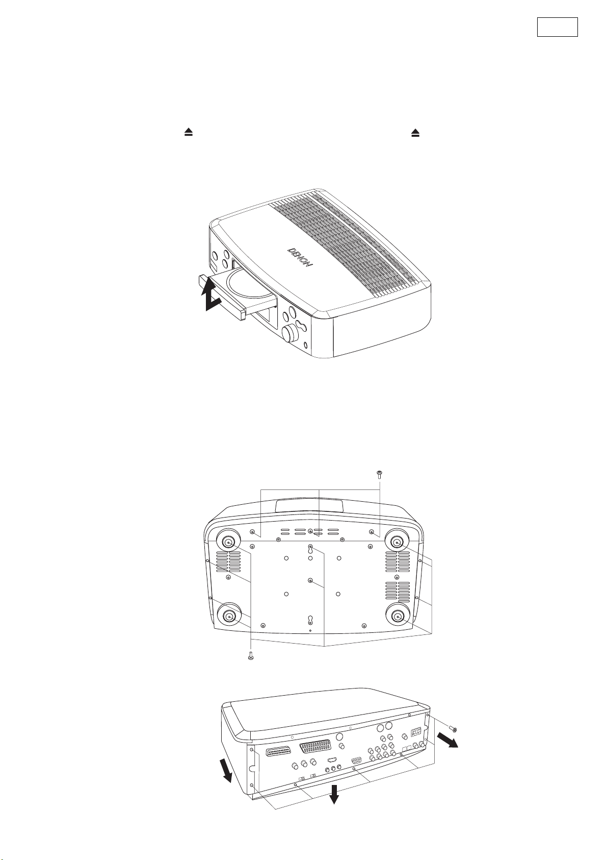
DISASSEMBLY
(Follow the procedure below in reverse order when
reassembling.)
1. Loader Panel
(1) Switch on, and press [ (OPEN/CLOSE)] button
to open the Disc tray.
(2) Detach the Loader Panel by lifting.
各部のはずしかた
(組み立てるときは、逆の順序でおこなってください。)
1. ローダーパネルのはずしかた
(1) 電源を入れ「 (OPEN/CLOSE)」ボタンを押して、
ディスクトレイを開きます。
(2) ローダーパネルを持ち上げてはずします。
2. Side Panel, Bottom Cover
(1) Remove 13 bottom screws.
(2) Remove 7 rear screws, then detach Side Panel and
Bottom Cover.
2. サイドパネル、ボトムカバーのはずしかた
(1) 底面よりネジを 13 本はずします。
(2) 裏面よりネジを 7 本はずし、サイドパネル、ボト
ムカバーをそれぞれ矢印の方向へはずします。
3
Page 4
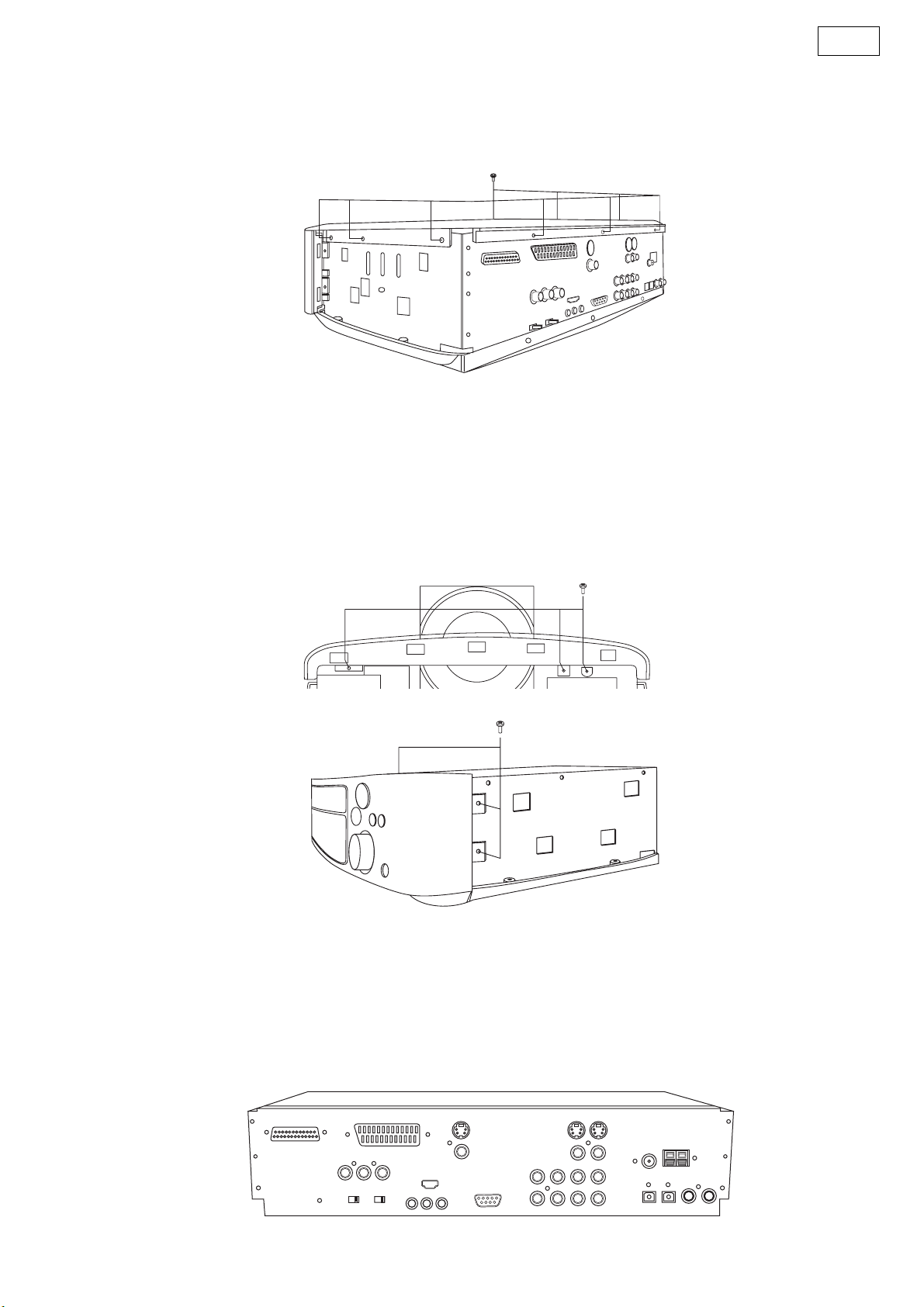
S-301
3. Top Cover
(1) Remove 9 top screws, then detach Top Cover.
4. Front Panel Ass’y
(1) Remove 3 Front panel screws, then detach P.W.B.
and chassis.
(2) Remove 4 Front panel side screws, then detach the
Front Panel Ass’y.
3. トップカバーのはずしかた
(1) トップカバーを止めている上部のネジ 9 本をはず
し、トップカバーを矢印の方向へはずします。
4. フロントパネルのはずしかた
(1) フロントパネルからの基板とシャーシを止めてい
るネジを 3 本はずします。
(2) フロントパネル側面を止めているネジ 4 本(左右
各 2 本)をはずし、フロントパネルを矢印の方向
へはずします。
5. Front Panel Ass’y
(1) Remove each terminal screws, Back Panel screws
and Chassis screws, then detach the Back Panel.
5. バックパネルのはずしかた
(1) 各端子を止めているネジおよびバックパネルと
シャーシを止めているネジをはずし、バックパネ
ルをはずします。
4
Page 5
S-301
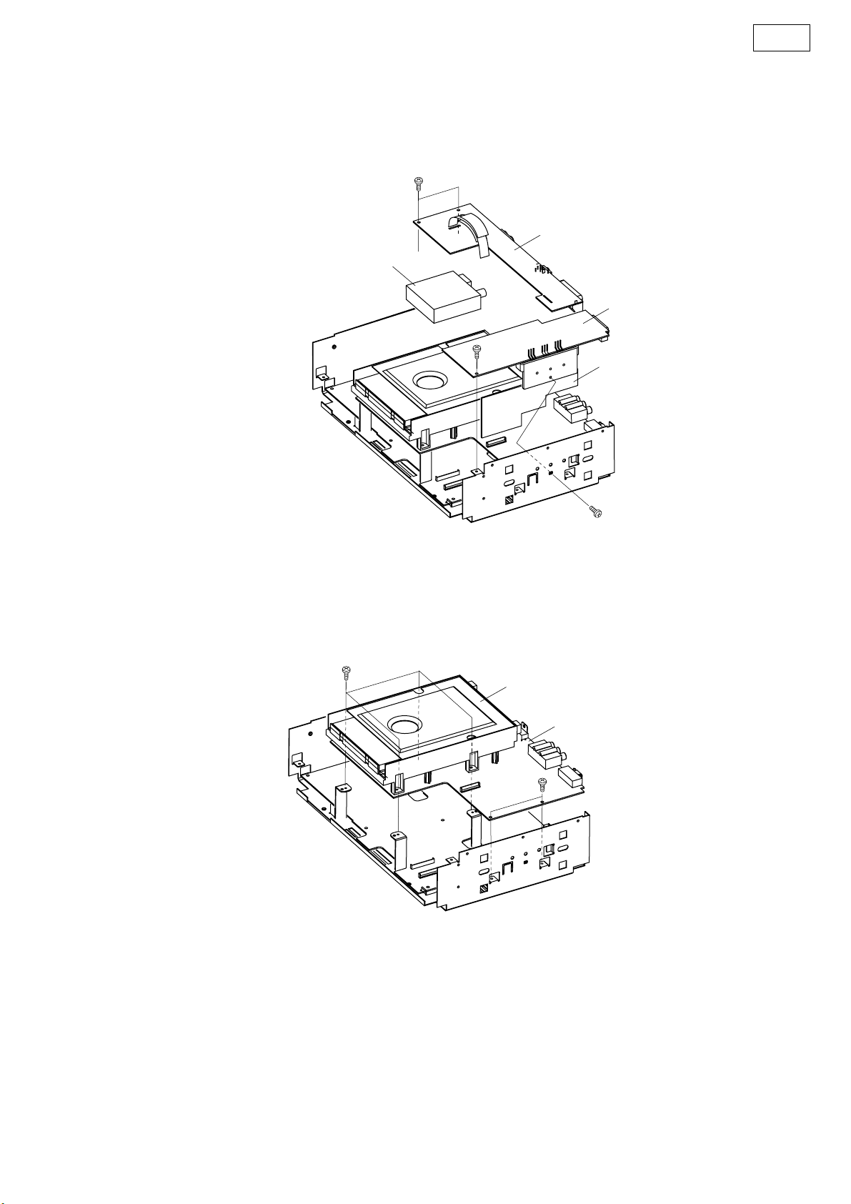
6. DVD Mecha
(1) Remove 4 screws, then detach P.W.B.(1U-3695-1,
1U-3695-2, 1U-3695-3) and TUNER PACK.
TUNER PACK
6. DVD メカの取りはずしかた
(1) ネジを 4 本はずし、1U-3695-1 基板と 1U-3695-2
基板と 1U-3695-3 基板と TUNERPACK をはずしま
す。
1U-3695-3
1U-3695-1
1U-3695-2
(2) Remove 6 screws, then detach 1uU-3692 P.W.B.
with DVD mecha from bottom chassis.
(2) ネジを 6 本はずし、1U-3692 基板と DVD メカを
一体でシャーシよりはずします。
D
VD mecha
1U-3692
5
Page 6
S-301
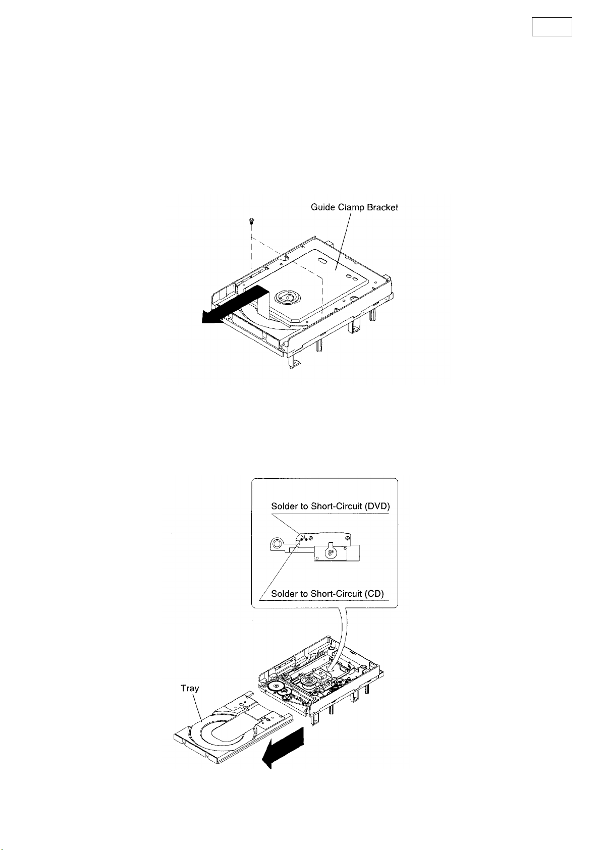
7. Traverse Unit Disassembly
Caution: The optical pickup can be damaged easily
by static electricity charged on human body. Take
necessary anti-static measures when repairing
around the optical pickup.
7.1. Guide Clamp Bracket disassembly
(1) Remove 2 screws.
(2) Remove Guide Clamp Bracket to arrow direction.
7. トラバースユニットのはずしかた
注意:光ピックアップは、人体に帯電した静電気等で
静電破壊することがあります。光ピックアップ周辺を
修理する際は、必要な静電対策を行ってください。
7.1. ガイドクランプブラケットのはずしかた
(1) ねじ 2本をはずします。
(2) ガイドクランプブラケットを矢印の方向にとりは
ずします。
7.2. Tray disassembly
(1) Remove to arrow direction.
(2) Solder the short-circuit (see in the frame).
7.2. トレイのはずし方
(1) 矢印の方向にとりはずします。
(2) 半田付けショートを行います。(枠内図参照 )
6
Page 7
S-301
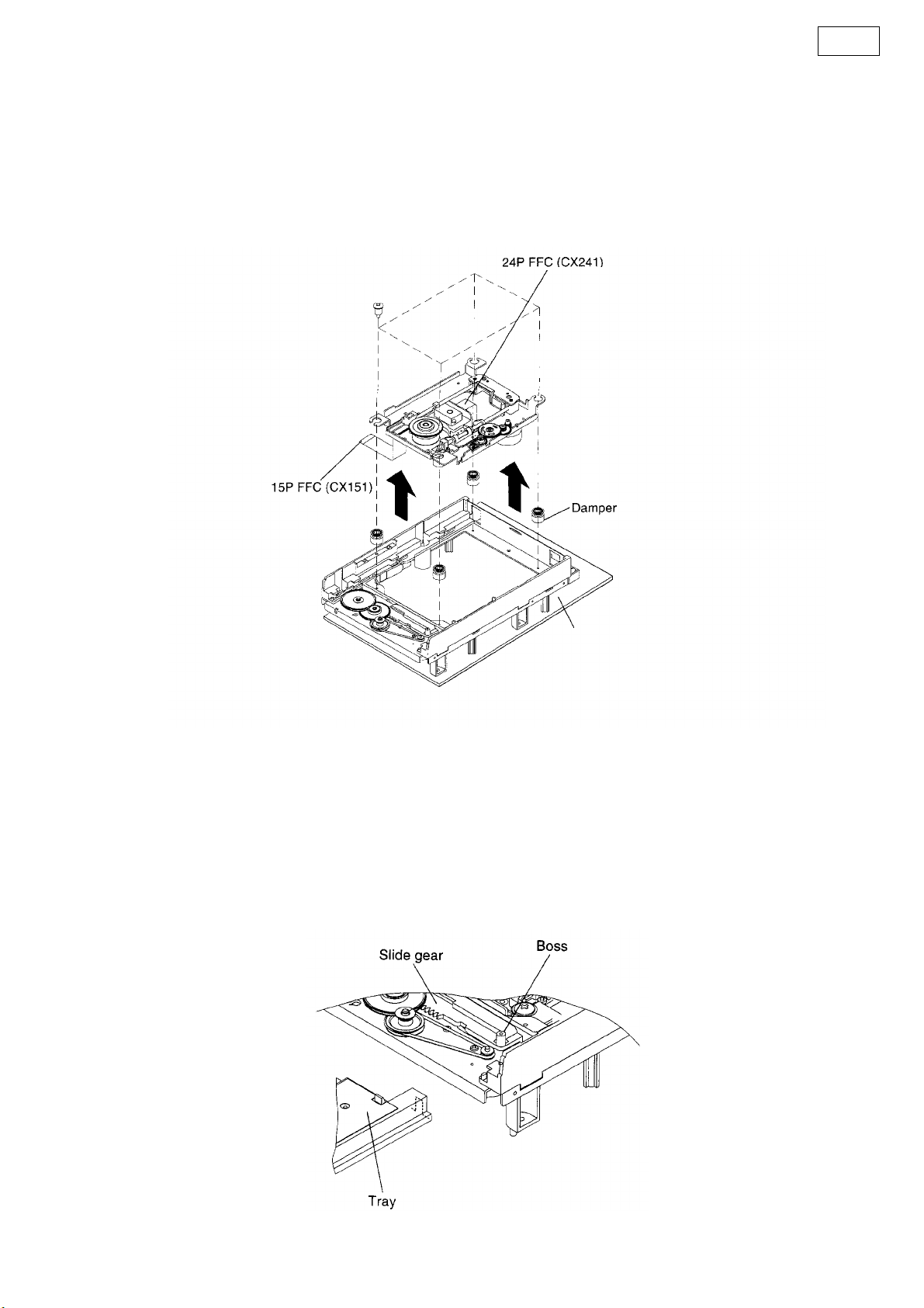
7.3. Traverse Unit disassembly
(1) Remove 24P FFC (CX241), 15P FFC (CX151), 5P
PH WIRE (CX051) connecting with from 1U-3692
P.W.B.
(2) Remove 4 screws fixing Damper.
(3) Remove Traverse Unit to arrow direction.
7.3. トラバースユニットのはずしかた
(1) 1U-3692 基板に接続している 24PFFC(CX241)、
15PFFC(CX151)、5PPHワイヤ(CX051) をはずし
ます。
(2) ダンパーを固定しているねじ 4本をはずします。
(3) トラバースユニットを矢印の方向にとりはずしま
す。
Note for disassembly Traverse Unit
(1) When assembling, reverse the order of the above.
(2) When inserting Tray, confirm boss on Slide Cam
set to ditch of the Tray (Compare with below drawing).
1U-3692 P.W.B.
トラバースユニット分解の注意
(1) 組み立てるときは、上記の逆の順序で行ってくだ
さい。
(2) トレイ組込み時、スライドカムのボスがトレイの
溝に合っているか確認してください。(下図参照)
7
Page 8
S-301
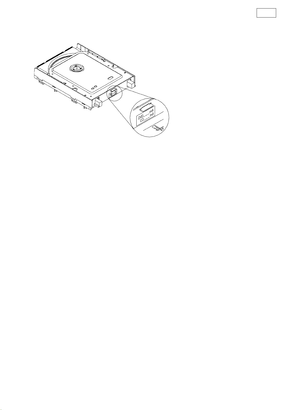
DIAGNOSTICS OF OPTICAL PICKUP AND REPLACING TRAVERSE UNIT
Make failure diagnostics of the Optical Pickup as follows.
If the laser drive current (Iop) becomes more than 1.5 times of
the initial value, the Optical Pickup should be replaced.
The laser drive current is registered on the seal attached to the
rear of the Mecha.Unit.
In case of replacing the Pickup, change the whole part of the
Traverse Unit.
No mechanical adjustment is necessary after the replacement.
Example:
例:
DVD 30mA
CD 30mA
光ピックアップの故障診断とトラバース
ユニットの交換
次の順序で故障診断を行ってください。
レーザー駆動電流 Iop 値が初期値の 1.5 倍以上になっている
場合は光ピックアップ交換の目安となります。
レーザー駆動電流初期値は、メカの後部のシール上に記入さ
れています。
ピックアップ交換の場合は、トラバースユニット単位での交
換となります。メカの調整は不要です。
Disc no read, unsteady playback, etc.
Laser drive current (Iop) check
HF wave form check
(Refer to WAVE FORMS)
Present value exceeds the initial value by 1.5 times
Traverse Unit replacing
(See page 6, 7 for details)
ディスクを読み込まない
スムーズに再生しない、等
レーザー駆動電流 Iop 値の確認
HF 波形の確認
(WAVEFORMS参照)
現在値が初期値の
1.5 倍になっている
トラバースユニット交換
(詳細は 6,7 ページ)
Laser current registering after replacement.
Step: Disc playback
Write the measured value on the seal attached to the
Mecha. Unit
* As to the measuring method, refer to page 9, 10.
交換後のレーザー電流記入
手順:ディスクを再生
その時の Iop 値をメカ後方のシールの上に重ねて貼る
等で更新する。
*Iop の測定方法は、9,10 ページ参照。
8
Page 9
S-301
1. Label Indication of SACD Mechanism.
2. Note for Handling the Laser Pick-Up
The protection for the damage of laser diode.
If you want to change the optical device unit from any other
units, you must keep the following.
(1) It should be done at the desk already took measures the
static electricity in care of removing the OPU's (Optical
device unit) connector cable.
(2) Workers should be put on the "Earth Band".
(3) It should be done to add the solder to the short land to
prevent the broken Laser diode before removing the 24P
FFC cable.
(4) Don't touch OPU's connector parts carelessly.
1. SACD メカのラベル表示
Laser current consumption value
DVD
㧖㧖㧖
㧖㧖㧖
mA, CD
mA, CD
ex) DVD
ࠩ㚟േ㔚ᵹ୯
㧕
㧖㧖㧖
㧖㧖㧖
mA
mA
2. レーザーピックアップの取扱注意
レーザーダイオードの破壊防止。
光素子ユニットを交換するときは、以下を遵守してくださ
い。
(1) 光素子ユニットの接続ケーブルをはずすときは、静電対
策を行ったデスク上で作業してください。
(2) 作業者は、リストストラップを使用してください。
(3) レーザーダイオードの破壊防止のため、24PFFC ケーブ
ルをはずす前にランドを半田付けショートしてくださ
い。
(4) 光素子ユニットのコネクタ部に触れないでください。
3. Replacement of the Laser Pick-up
(Traverse Unit)
Check the Iop (Laser drive current)
If the present Iop (current) value exceeds.+150% of the initial value, replace the Traverse unit (Laser Pick-up) with a
new one.
4. Iop Measurement Method
When measuring Laser drive current (Iop), playback the
discs (CD,DVD) described below, measure Iop for CD Laser
and DVD Laser by the test point (+5V-A2~ LD (CD), LD
(DVD))on the Main P.W.B.
Test Disc : DVD/DVDT-S01 or commercially available
discs.
: CD/TCD-784 (manufactured by ALMEDIO
INC) or commercially available discs.
3. レーザーピックアップ ( トラバースユニッ
ト ) の交換
Iop( レーザー駆動電流)をチェックします。
現在の Iop値が初期値の 150%を越えている場合、トラバー
スユニット(レーザーピックアップ)を交換してください。
4. Iop の測定方法
レーザー駆動電流を測定する場合、下記のディスク
(CD,DVD) を再生します。
Main 基板上のテストポイント(+5V-A2 〜LD(CD),LD(DVD))
にて、CD レーザーと DVD レーザーの Iop を測定してくだ
さい。
テストディスク: DVD/DVDT-S01または市販同等ディスク
: CD/TCD-784(ALMEDIO社製)または市販
同等ディスク
9
Page 10
S-301
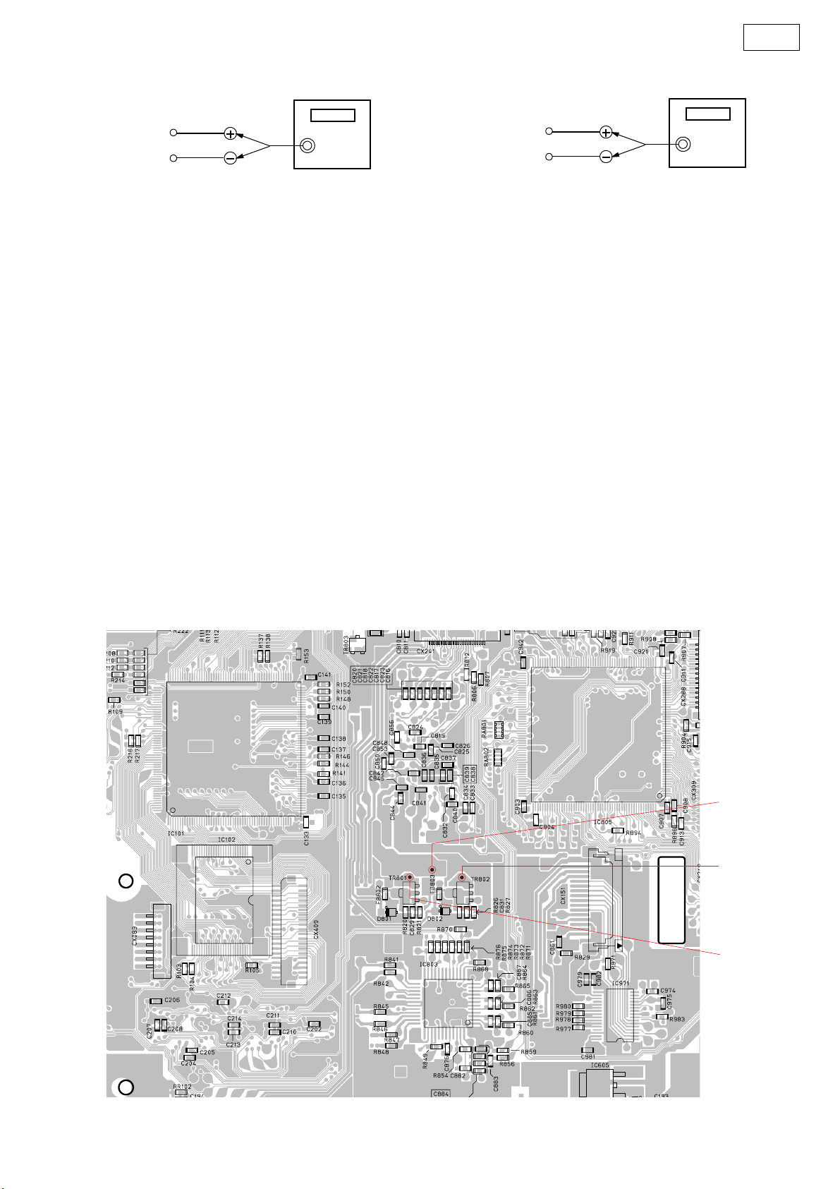
4.1. DVD Laser current measurement
LD (DVD)
+5V-A2
Oscilloscope
(1) Connect the oscilloscope to +5V-A2 of test point for
GND side and LD (DVD) of test point for signal side.
(2) Playback the multi layer track 1 of the DVD Test Disc.
(3) Measure the voltage between +5V-A2 and LD (DVD),
calculate Iop by the formula as shown below.
Iop
Measurement Voltage Value
-----------------------------------------------------------------------------=
14 (Resistance value)
4.2. CD Laser current measurement
(1) Connect the oscilloscope to +5V-A2 of test point for
GND side and LD (CD) of test point for signal side.
(2) Playback the track 1 of the CD Test Disc.
(3) Measure the voltage between +5V-A2 and LD (CD), cal-
culate Iop by the formula as shown below.
4.1. DVD レーザー電流測定
LD (DVD)
+5V-A2
Oscilloscope
(1) オシロスコープをテストポイント +5V-A2(GND) と
LD(DVD)( 信号 ) へ接続します。
(2) DVDテストディスクのマルチレイヤートラック 1 を再生
します。
(3) +5V-A2 と LD(DVD) 間の電圧を測定し、次式により Iop
を算出します。
Iop
測定電圧値
-----------------------------=
14(抵抗値)
4.2. CD レーザー電流測定
(1) オシロスコープをテストポイント +5V-A2(GND) と
LD(CD)( 信号 ) へ接続します。
(2) CD テストディスクのトラック 1 を再生します。
(3) +5V-A2 と LD(CD) 間の電圧を測定し、次式より Iop を
算出します。
Iop
Measurement Voltage Value
-----------------------------------------------------------------------------=
11.75 (Resistance value)
Iop
測定電圧値
------------------------------------=
11.75(抵抗値)
+5V_A2
LD(CD)
1u-3692 foil side
10
LD(DVD)
Page 11
S-301
Special operating procedures
1. Initialization
※ This initializes the data for the function, volume,
DVD mechanism (RL-874), etc.
(1) Check that the AC cord is disconnected from the
power outlet. (AC OFF)
(2) While pressing the FUNCTION and OPEN/CLOSE
( ) buttons on the main unit, plug the AC cord into
the power outlet. (AC ON)
(3) Check that the entire display and all the LEDs light,
then release the FUNCTION and OPEN/CLOSE
() buttons.
(4) After about 3 seconds, "INITIALIZE" appears on the
display.
(5) After initialization is complete (when "INITIALIZE"
turns off), the function is set to "DVD" and the volume level is set to -∞ ("-dB" is displayed).
2. System check mode
※ Use this to display the version information, etc.
(1) In the standby mode, while pressing the STOP ( )
and A.FWD ( ) buttons on the main unit, press
the ON/STANDBY button.
(2) Press the STATUS button on the remote control
unit (RC-1005 or RC-1006) to display the following
information, in this order: Time (TIME) → System
microprocessor version (SYS Ver) → Date of system microprocessor version updating (SYS Date)
→ DSP version (DSP Ver) → Date of DSP version
updating (DSP Date) → Date of drive microprocessor version updating (Dr Date) → ESS version (Ess
Ver) → Date of ESS version updating (Ess Date) →
Region number (Region No.)
(3) To cancel, unplug the AC cord. (AC OFF)
NOTE 1: The DVD mechanism driver version and
ESS version are not displayed unless the
function is once set to DVD.
特殊操作方法
1. 初期化
※ ファンクション、VOL 及び DVD メカ (RL-874) 等の
データを初期化します。
(1) ACコードがコンセントより外れていることを確認
します。(ACOFF)
(2) 本体の FUNCTION ボタンと OPEN/CLOSE( ) ボタ
ンを押しながら、AC コードをコンセントに接続
(ACON) します。
(3) ディスプレイと LED の全点灯を確認したら、本体
の FUNCTION ボタンと OPEN/CLOSE( ) ボタンを
離します。
(4) 約 3 秒後、ディスプレイに "INITIALIZE" が表示され
ます。
(5) 初期化完了 ("INITIALIZE" 消灯 ) 後、FUNCTION は
"DVD"、VOL位置は- ∞ ( 表示は "---dB") となります。
2. システムチェックモード
※ バージョン表示等をおこないます。
(1) STANDBY 時、本体の STOP( )ボタンと A.FWD
( )ボタンを押しながら、ON/STANDBY ボタ
ンを押します。
(2) リモコン(RC-1005orRC-1006)の STATUS ボタン
を押すことにより
時間(TIME)→システムマイコンのバージョン(SYS
Ver) →システムマイコンのバージョンアップ日
(SYSDate)→DSP のバージョン (DSPVer) → DSP
のバージョンアップ日(DSPDate)→ドライブマイ
コンのバージョンアップ日 (DrDate) →ESS のバー
ジョン (EssVer) → Ess のバージョンアップ日 (Ess
Date) →地域番号 (RegionNo.)
の順に表示されます。
(3) 解除するにはAC コードを抜きます。(ACOFF)
( 注 1) DVD メカのドライブバージョン表示、ESS
のバージョン表示については、1 度ファン
クッションを DVD にしないと表示されま
せん。
11
Page 12

S-301
ADJUSTMENT
1. SETTING
(1) Connect the oscilloscope to the Y-signal, PB-signal and
C
B-signal, PR-signal and CR-signal of ZONE2 COMPO-
NENT OUT terminal and each terminate at 75 Ohms.
※ Use the 75 Ohms resistance must be 1%
(2) DVD test disc : DVDT-S01
(3) S OUT of DVD player is connected to AUX1 S IN.
2. Before Adjustment
2.1. Setting the Oscilloscope as below.
(1) PB/CB, PR/CR
(a) TIME/DIV : 10μs
(b) VOLT/DIV : 100mV
(Use the probe : x10 )
(2) Y
(a) TIME/DIV : 10μs
(b) VOLT/DIV : 200mV
(Use the probe : x10 )
Power on. Power Supply
USA & Canada : 120V
Europe : 230V
Japan : 100V
China & Korea : 220V
調整
1. セッティング手順
(1) セットの ZONE2COMPONENTOUT の端子(Y,PB/CB,
PR/CR)をそれぞれオシロスコープ(終端抵抗:75Ω)
に接続します。
※ 75Ω 抵抗は 1%品を使用する事。
(2) DVD テストディスク:DVDT-S01 を用意します。
(3) DVD プレーヤーの SOUT を AUX1SIN に接続します。
2. 調整のまえに
2.1. オシロスコープを下記に設定
(1) PB/CB,PR/CR
(a) TIME/DIV : 10μs
(b) VOLT/DIV : 100mV
(プローブ x10 使用)
(2) Y
(a) TIME/DIV : 10μs
(b) VOLT/DIV : 200mV
(プローブ x10 使用)
電源電圧 : 100V
2.2. Setup the DVD player and confirmation of the
stators
(1) Set to "INTERLACED" mode at the COMPONENT OUT.
(2) Confirm the DVD player’s out put level is equal as the
item 2.4. in following.
2.3. Preparation
(1) Push the FUNCTION knob to select "AUX1" input.
(2) Push [OPEN/CLOSE] button of DVD player, then open
the Disc Tray.
Set DVD test disc (DVDT-S01) on the Disc Tray, and
then push [CLOSE] button.
(3) DVD player FL display appear "STOP", push [PLAY] but-
ton to playback DVD.
(4) Push the [DISPLAY] button of remote control of DVD
player unit and then appear the ON-Screen Display (GUI)
on the monitor TV.
(5) Push the [+10] and [2] button, select Title 12 of DVD.
(6) Push the [ENTER] button, playback Title 12.
(color bar 75%)
2.2. DVD プレーヤの設定と確認
(1) COMPONENTOUTの設定を"インターレース "にします。
(2) DVD プレーヤーの出力が以下 2.4. に合っていることを
確認します。
2.3. 準備手順
(1) FUNCTION ノブを押し、入力を "AUX1" に切り替えます。
(2) DVD プレーヤーの「OPEN/CLOSE」ボタンを押しトレイ
を開き、トレイ上に DVD テストディスク(DVDT-S01)
をセット後、「CLOSE」ボタンを押します。
(3) DVD プレーヤーの表示管上に "STOP" が表示されてか
ら、「PLAY」ボタンを押し、ディスクを再生します。
(4) DVD プレーヤーのリモコンの「DISPLAY」ボタンを押
しグラフィカル・ユーザー・インターフェイス (GUI) 画
面を出します。
(5) 番号ボタンの「 +10 」 , 「 2 」ボタンを押し、Title12 を選択
します。
(6) 「ENTER」ボタンを押し、Title12 を再生します。
(75%カラーバー信号)。
12
Page 13
S-301
2.4. Procedure
(1) Adjust the signal of COMPONENT OUT by the wave of
oscilloscope.
(a) Target, Y-signal
Point : 1U-3695-3 VR601
Adjustment Value : 714 ± 35mV
Waveform
Y
Y-signal COMPONENT OUT
(b) Target, P
Point : 1U-3695-3 VR602
Adjustment Value : *525 ± 25mV
Waveform
B/CB-signal
PB
2.4. 手順
(1) COMPONENTOUTの信号レベルをオシロスコープ上の
波高値で調整します。
(a) Y 信号レベル
調整個所 : 1U-3695-3VR601
調整値 : 714 ± 35mV
波形
Y
COMPONENTOUT の Y 信号レベル
B/CB 信号レベル
(b) P
調整個所 : 1U-3695-3VR602
調整値 : 525 ± 25mV
波形
PB/CB
PB/CB-signal COMPONENT OUT
(c) Target, PR/CR-signal
Point : 1U-3695-3 VR603
Adjustment Value : *525 ± 25mV
Waveform
PR/CR
PR/CR-signal COMPONENT OUT
* : 486 ± 10mV for U.S.A. & Canada model
COMPONENTOUT の PB/CB 信号レベル
(c) PR/CR 信号レベル
調整個所 : 1U-3695-3VR603
調整値 : 525 ± 25mV
波形
PR/CR
COMPONENTOUT の PR/CR 信号レベル
13
Page 14
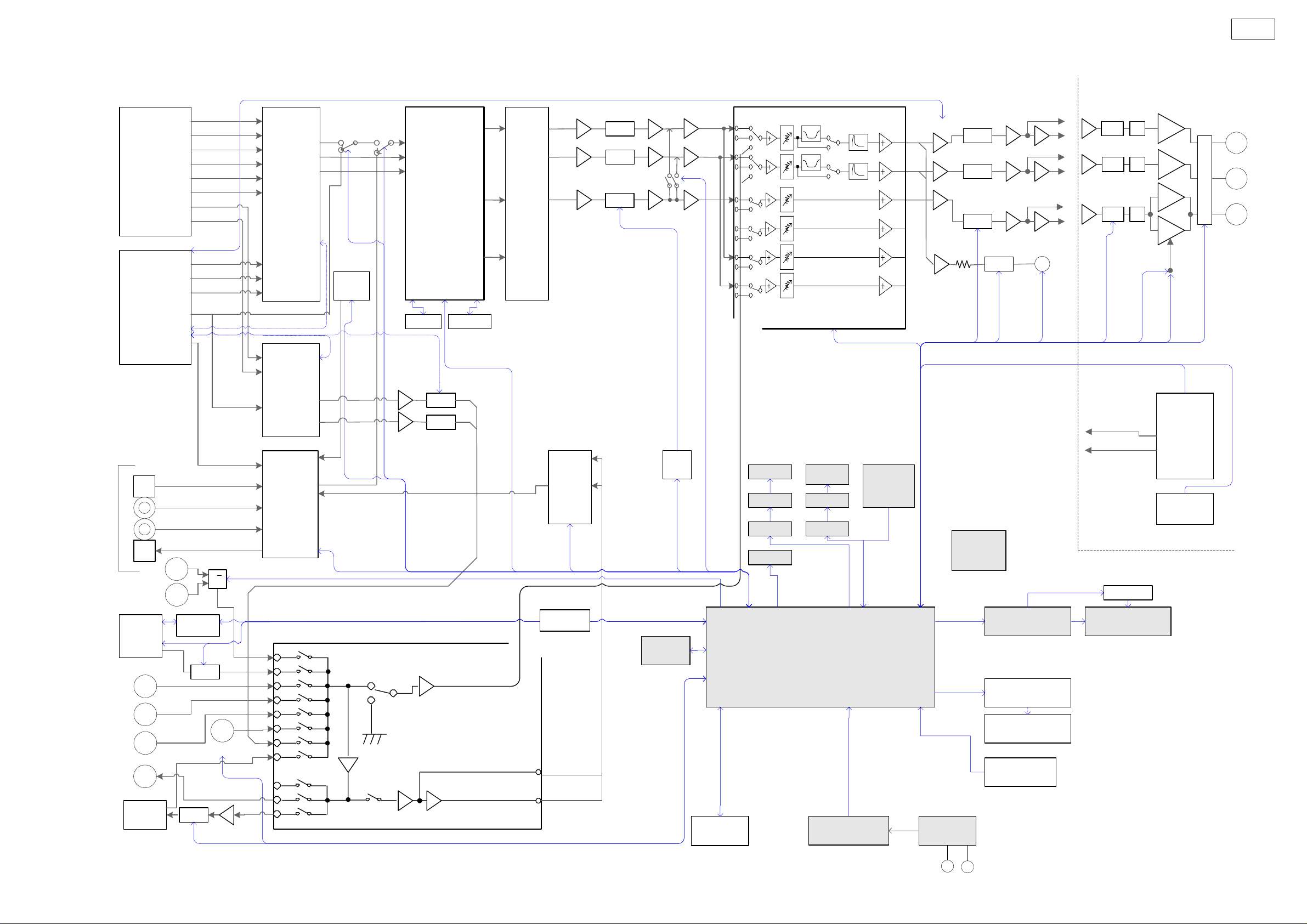
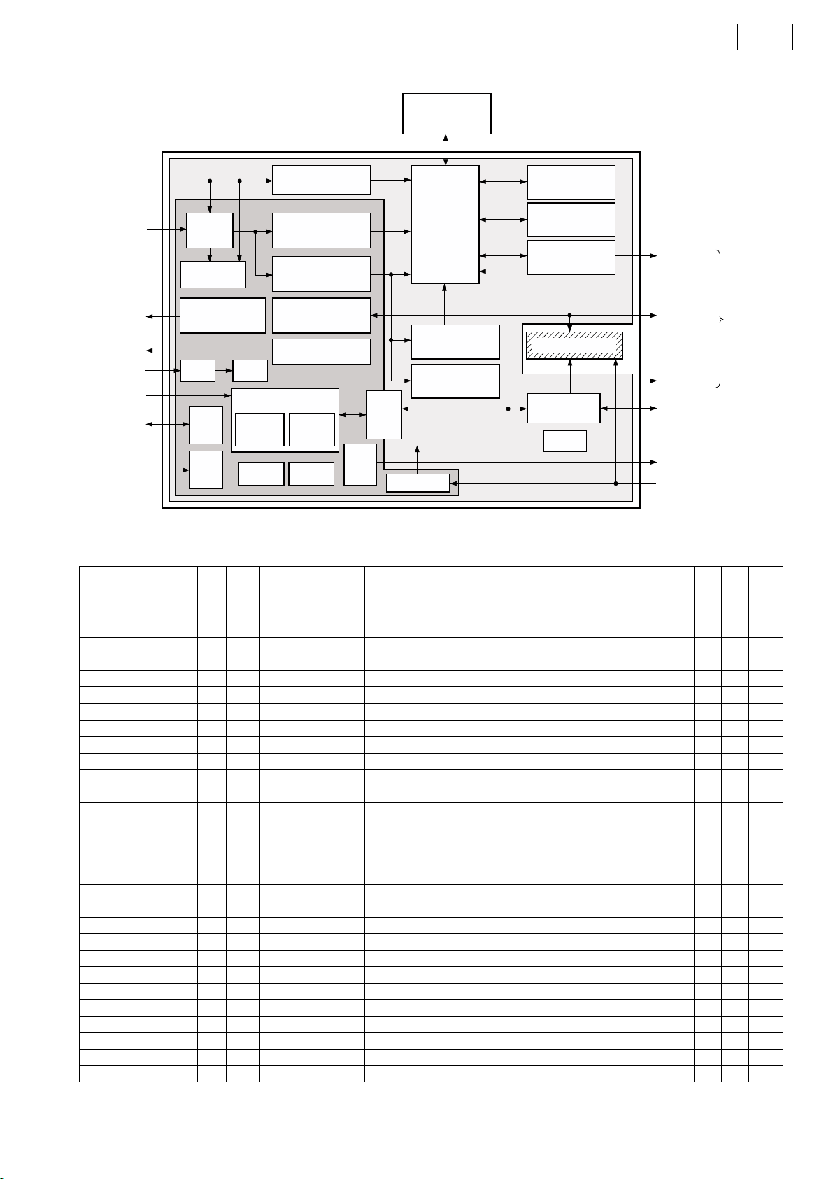
BLOCK DIAGRAM
S-301
㪜㫏㫋㪅
㪛㫀㪾㫀㫋㪸㫃㩷㪠㫅
㫏㪊
㪜㫏㫋㪅
㪘㫅㪸㫃㫆㪾㩷㪠㫅
㫏㪊
㪪㪘㪚㪛
㪛㪜㪚㪦㪛㪜㪩
㪚㪯㪛㪉㪎㪌㪊㪩
㪠㪉㪪㩷㪦㪬㪫
㪛㪭㪛
㪛㪜㪚㪦㪛㪜㪩
㪧㪅㪧㪚㪤㪆㪤㪧㪊㪆㪮㪤㪘
㪛㪜㪚㪦㪛㪜
㪜㪪㪍㪈㪊㪏
㪪㪧㪛㪠㪝㩷㪦㪬㪫
㪦㪧㪫
㪠㪥㪈
㪚㪦㪘
㪠㪥
㪚㪦㪘
㪠㪥
㪦㪧㪫
㪦㪬㪫
㫀㪧㫆㪻
㫀㫅
㪬㪪㪙
㫀㫅
㪫㪬㪥㪜㪩
㪫㪬㪥㪜㪩
㪧㪘㪚㪢
㪧㪘㪚㪢
㪣㪚㪎㪉㪈㪊㪈
㪣㪚㪎㪉㪈㪊㪈
㪘㪥㪘
㪘㪥㪘
㪘㪥㪘
㪘㪥㪘
㪦㪬㪫
㪣㪆㪩
㪣㪆㪩
㪠㪥
㪣㪆㪩
㪠㪥
㪣㪆㪩
㪠㪥
㪣㪆㪩
㪪㪚㪘㪩㪫
㪦㪬㪫
㩿㪜㪉㩷㫆㫅㫃㫐㪀
㪛㪪㪛㩷㪦㪬㪫
㪛㪪㪛㩷㪝㪣
㪛㪪㪛㩷㪝㪩
㪛㪪㪛㩷㪪㪣
㪛㪪㪛㩷㪪㪩
㪛㪪㪛㩷㪚
㪛㪪㪛㩷㪪㪮
㪛㪪㪛㩷㪤㪠㪯㩷㪣
㪛㪪㪛㩷㪤㪠㪯㩷㪩
㪧㪚㪤㩷㪝㪣㪆㪝㪩
㪧㪚㪤㩷㪪㪣㪆㪪㪩
㪧㪚㪤㩷㪚㩷㪆㪪㪮
㪧㪚㪤㩷㪤㪠㪯㩷㪣㪆㪩
㪩㪯㪇㪄㪍䉕㪪㪜㪣㪜㪚㪫䈚䈩ജ
㪪㪮
㪩㪛㪪
㪣㪚㪎㪉㪎㪉㪇
㪤㪬㪫㪜
㪘㪥㪘
㪠㪥
㪧㫆㫉㫋㪸㪹㫃㪼㩷㪠㫅
㩿㪽㫉㫆㫅㫋㩷㫇㪸㫅㪼㫃㪀
㪪㪚㪘㪩㪫㩷㪠㪥
㪣㪆㪩
㪤㪬㪫㪜
㪝㪩㪠㪥㩷㪪㪮
㪩㪜㪚㩷㪦㪬㪫㪈
㪂
㪪㪚㪘㪩㪫㪶㪤㪬㪫㪜
㪛㪪㪛㩷㪠㪥
㪧㪚㪤㩷㪠㪥
㪩㪯㪈
㪪㪘㪥㪶㪛㪦
㪪㪘㪥㪶㪛㪠
㪪㪘㪥㪶㪚㪢
㪪㪘㪥㪶㪚㪜
㪧㪚㪤㩷㪝㪣㪆㪝㪩
㪧㪚㪤㩷㪚㪆㪪㪮
㪛㪪㪛
㪧㪚㪤㩷㪪㪣㪆㪪㪩
㪛㪸㫋㪸㩷㪪㪼㫃㪼㪺㫋㫆㫉
㪛㪪㪛㪄㪧㪚㪤㩷㪚㫆㫅㫍㪼㫉㫋
㪛㪪㪛㪆㪜㪯㪫
㪪㪜㪣㪶㪝㫊㪈
㪠㪥㪠㪫
㪜㪯㪫
㪛㪪㪛㪆㪧㪚㪤
㪛㪘㪚
㪛㪪㪛㪈㪎㪐㪈
㩿㪩㪼㪺㫆㫌㫋㪆
㪪㪚㪘㪩㪫㪀
㪩㪯
㪩㪯
㪛㪠㪩
㪩㪯
㪣㪚㪏㪐㪇㪌㪎
㪆㪫㪶㪤㪬㪫㪜
㪆㪪㪰㪩
㪆㪫㪬㪥㪜㪛
㪪㪫㪜㪩㪜㪦
㪩㪜㪚㩷㪦㪬㪫
㪤㪠㪯
㪛㪘㪫㪘
㪚㪣㪢
㪩㪜㪪㪜㪫
㪚㪜
㪬㪪㪙
㪪㪧㪛㪠㪝
㪛㪠㪩
㪘㪛
㪠㪥
㪤㫌㫃㫋㫀 㪤㫌㫃㫋㫀
㪛㪠㪩
㪤㪠㪯㪆㪤㪬㪣㪫㪠
㪠㪉㪪㩷㪛㪘㪫㪘
㪦㪬㪫
㪬㪪㪙
㪤㪦㪛㪬㪣㪜
㪬㪪㪙㪶㪫㪯㪛
㪬㪪㪙㪶㪩㪯㪛
㪬㪪㪙㪶㪚㪣㪢
㪬㪪㪙㪶㪩㪪㪫
㪬㪪㪙㪶㪚㪜
㪬㪪㪙㪶㪩㪜㪨
㪬㪪㪙㪶㪤㪦㪛㪜
㪬㪪㪙㪶㪧㪦㪮㪶㪦㪥
㪩㪜㪚㩷㩷㪣㪆㪩
㪛㪠㪩㪆㪚㪦㪛㪜㪚㪶㪚㪣㪢
㪛㪠㪩㪶㪚㪜
㪛㪠㪩㪆㪚㪦㪛㪜㪚㪶㪛㪠㪥
㪛㪠㪩㪶㪛㪦㪬㪫
㪛㪠㪩㪶㪩㪪㪫
㪆㪠㪥㪫㪈
㪠㪥㪧㪬㪫
㪪㪜㪣㪜㪚㪫㪦㪩
㪂
㪤㪬㪣㪫㪠㪆㪛㪠㪩
㪠㫅㫇㫌㫋㩷㪘㪫㪫
㪇㪆㪄㪍㪆㪄㪐㪆㪄㪈㪉㪻㪙
㪄
㪛㪪㪧
㪪㪿㪸㫉㪺㩷㪜㪯㩿㪨㪝㪧㪀
IN
DATP20:FL/FR
DAIP19:C/SW
DAIP18:SL/SR
OUT
DAIP16:FL/FR
DAIP16:0/SW
DAIP15:0/0
DAIP14:RECL/RECR
㪍㪋㪤
㪪㪛㪩㪘㪤
㪘㪤㪬㪫㪜
㪤㪬㪫㪜
㪤㪬㪫㪜
㪂
㪄
㪣㪆㪩
㪪㪮
㪩㪜㪚㩷㪣㪆㪩
㪈㪍㪤㩷㪩㪦㪤
㪝㪣㪘㪞㪊㪘
㪙㪬㪪㪰㪈
㪘㪚㪢㪈
㪩㪦㪤㪶㪩㪪㪫
㪛㪪㪧㪶㪩㪪㪫
㪭㪧㪧
㪩㪆㪮
㪙㪬㪪㪰㪶㪜㪧㪩㪦㪤
㪘㪥㪘㪣㪦㪞
㪛㪠㪩㪜㪚㪫
㪜㪣㪜㪚㪅㪭㪩㩷㩷㪙㪛㪊㪏㪈㪈
㩿㪉㪆㪉㪀
㪘㪆㪛㩷㪦㪬㪫㩷㪄
㪘㪆㪛㩷㪦㪬㪫㩷㪂
㪘㪛㪈㪏㪊㪎
㪏㪺㪿
㪚㪦㪛㪜㪚
㪈㪆㪉
㩿㪛㪘㪚㪀
㪛㪪㪧㪶㪠㪦㪶㪧㪦㪮
㪛㪪㪧㪶㪚㪦㪩㪜㪶㪧㪦㪮
㪛㪪㪧㪶㪦㪪㪚㪶㪦㪥
㪛㪪㪧㪤㪠㪪㪦
㪛㪪㪧㪤㪦㪪㪠
㪛㪪㪧㪪㪧㪠㪚㪣㪢
㪛㪪㪧㪪㪧㪠㪚㪪
㩿㪛㪠㪩㪆㪚㪦㪛㪜㪚㪶㪚㪣㪢㪀
㩿㪛㪠㪩㪆㪚㪦㪛㪜㪚㪶㪛㪠㪥㪀
㪚㪣㪘㪫㪚㪟
㪚㪦㪛㪜㪚㪶㪩㪪㪫
㪂㪌㪭㪆㪂㪊㪅㪊㪭
㪘㪛㪈㪏㪊㪎
㪏㪺㪿
㪚㪦㪛㪜㪚
㪉㪆㪉
㩿㪘㪛㪚㪀
㪚㫆㫅㫍㪅
㪝㫀㫃㫋㪼㫉
㪣㪆㪩
㪪㪮
㪛㪘㪚㪶㪤㪬㪫㪜
㪤㪬㪫㪜
㪤㪬㪫㪜
㪤㪬㪫㪜
㪪㪬㪙㪶㪪㪬㪤
㪜㪉㪧㪶㪛㪠
㪜㪉㪧㪶㪛㪦
㪜㪉㪧㪶㪚㪪
㪜㪉㪧㪶㪚㪢
㪄
㪄
㪄
㪣㪦㪞㪠㪚
㪜㪜㪧㪩㪦㪤
㪙㪩㪐㪊㪣㪏㪍
㩿㪈㪍㫂㪀
㪄
㪄
㪄
㪙㪪㪜
㪜㪩㪩㪤㪬㪫㪜
㪪㪜㪣㪚㪣㪢
㪦㪧㪶㪚㪣㪢
㪦㪧㪶㪚㪜
㪦㪧㪶㪛㪦
㪦㪧㪶㪛㪠
㪙㪜㪶㪦㪥
㪛㪝㪩㪪㪫
㪧㪣㪣㪶㪩㪪㪫
㪛㪭㪛㪶㪩㪪㪫
㫋㫆㩷㪛㪭㪛㩷㪛㫉㫀㫍㪼㪆
㪭㫀㪻㪼㫆㩷㪙㪣㪦㪚㪢
㪘㪥㪘㪣㪦㪞
㪛㪠㪩㪜㪚㪫
㪚㪣㪪㪶㪪㪮
㪦㪧㪥㪶㪪㪮
㪦㪧㪥㪶㪛㪩㪭
㪚㪣㪪㪶㪛㪩㪭
㪭㪶㪚㪦㪥㪫
㪣㪛㪶㪚㪦㪥㪫
㪧㪩㪦㪞㪆㪫㪥㪫㪜㪩
㪭㪛㪜㪫㪈
㪭㪛㪜㪫㪉
㪇㩷㫋㫆㩷㪄㪈㪇㪊㪻㪙
㪠㫅㫇㫌㫋㩷㪞㪸㫀㫅㩷㪘㫄㫇㪑
㩷㪇㪆㪂㪍㪻㪙
㪉㪊㪉㪚
㪣㪤㪪㪉㪇㪉
㪎㪋㪣㪭㪇㪏
㪫㪩㪠㪞㪞㪜㪩
㪫㪩㪠㪞㪞㪜㪩
㪭㪠㪛㪜㪦㪶㪘
㪭㪠㪛㪜㪦㪶㪙
㪭㪠㪛㪜㪦㪶㪚
㪭㪠㪛㪜㪦㪶㪛
㪭㪤㪬㪫㪜㪈
㪭㪤㪬㪫㪜㪉
㪤㪸㫀㫅㩷㪭㫆㫃
㪈㪻㪙㩷㫊㫋㪼㫇
㪜㪣㪜㪚㪅㪭㪩㩷㩷㪙㪛㪊㪏㪈㪈
㩿㪈㪆㪉㪀
㪊㪏㪈㪈㪚㪣㪢
㪊㪏㪈㪈㪛㪘㪫㪘
㪩㪜㪤㪦㪫㪜
㪚㪯㪘㪈㪌㪈㪈
㪎㪋㪣㪭㪇㪏
㪪㪰㪪㪫㪜㪤㩷㫌㪚㪦㪤
㪤㪊㪇㪍㪉㪎㪝㪟㪧㪞㪧
㩿㪈㪉㪏㫇㫀㫅㩷㪊㪏㪋㫂㪆㪊㪈㫂㪀
㩷㪠㪆㪦
㪫㪯㪛㪉㪊㪉㪚
㪩㪯㪛㪉㪊㪉㪚
㪢㪜㪰㪇
㪢㪜㪰㪈
㪡㪦㪞㪶㪘
㪡㪦㪞㪶㪙
㪫㪘㪚㪫㩷㪪㪮㩷㪆
㪩㪦㪫㪅㪜㪥㪚㪦㪛㪜㪩
㪦㫌㫋㫇㫌㫋㩷㪞㪸㫀㫅㩷㪘㫄㫇㪑
㩷㪇㪆㪂㪉㪆㪂㪋㪆㪂㪍㪆㪂㪏㪆
㪂㪈㪇㪆㪂㪈㪉㪻㪙
㪩㪜㪤㪦㪚㪦㪥
㪩㪜㪚㪠㪜㪭㪜㪩
㪞㪧㪈㪬㪜㪉㪎㪈㪯
㪩㪜㪤㪦㪚㪦㪥
㪟㪞㪘㪠㪥
㪣
㪩
㪪㪮
㪟㪆㪧㪄㪈
㪘㪆㪛
㪛㪠㪤㪤㪜㪩㪶㪠㪥
㪧㪣㪘㪰㩷㪢㪜㪰
㪧㫉㪼㩷㪘㫄㫇
㪥㪡㪤㪉㪇㪍㪏
㪟㪆㪧㩷㪘㫄㫇㪄㪈
㪘㪺㫋㫀㫍㪼㩷㪙㫃㫆㪺㫂
㪜㪯㪫㪶㪛㪘㪫㪘
㪜㪯㪫㪶㪚㪣㪢
㪝㪣㪶㪛㪘
㪝㪣㪶㪚㪪
㪝㪣㪶㪚㪢
㪝㪣㪶㪩㪪㪫
㪫㪦㪬㪚㪟
㪪㪜㪥㪪㪦㪩㩷㪠㪚
㪤㪬㪫㪜
㪤㪬㪫㪜
㪤㪬㪫㪜
㪧㪩㪜㪶㪤㪬㪫㪜
㪪㫋㪸㫅㪻㪹㫐
㪪㪫㪦㪧㩷㪢㪜㪰
㪘㪛㪭㪄㪪㪊㪇㪈
㪛㫀㪽㪽㪅㩷㪦㫌㫋㫇㫌㫋
㪄 㪄
㪄 㪄
㪄 㪄
㪤㪬㪫㪜
㪟㪆㪧㩷㪤㪬㪫㪜
㪪㪜㪩㪠㪄㪧㪘㪩㪘
㪚㪦㪥㪭㪜㪩㪫㩷㪠㪚
㪙㪬㪉㪇㪐㪇㪝
㪝㪣㩷㪛㪩㪠㪭㪜㪩
㪤㪍㪍㪇㪇㪌㪘㪟㪧
㪝㪣㪛
㪛㪠㪤㪤㪜㪩
㪪㪜㪥㪪㪦㪩㩷㪠㪚
㪟㪆㪧
㪟㪧㩷㪪㪮
㪉㪌㪧㩷㪛㪄㪪㫌㪹
㪣㪦㪞㪠㪚㩷㪘㪆㪙㪆㪚
㪛㫀㪽㪽㪅㩷㪠㫅㫇㫌㫋
㪚㫌㫉㫉㪅㪣㫀㫄㫀㫋㫋㪼㫉
㪝㪣㪂
㪝㪣㪄
㪝㪩㪂
㪝㪩㪄
㪪㪮㪂
㪪㪮㪄
㪤㪬㪫㪜
㪤㪬㪫㪜 㪘㪆㪛
㪘㪣㪚㪆
㪧㪼㪸㫂㫀㫅㪾㪆
㪚㫌㫉㫉㪅㪣㫀㫄㫀㫋㫋㪼㫉
㪤㪬㪫㪜
㪧㪩㪜㪶㪤㪬㪫㪜
㪌㪇㪆㪍㪇
㪧㪅㪦㪥㪆㪦㪝㪝
㪂㪊㪈㪭
㪂㪌㪅㪇㪭㪶㪥㪪㪮
㪧㪚㪤㪄㪈㪏㪇㪊
㪭㫆㫃㫋㪸㪾㪼㩷㪸㪻㫁㫌㫊㫋
㪢㪜㪰㩷㪣㪜㪛
㪪㪫㪘㪥㪛㪙㪰㩷㪣㪜㪛
㪪㪊㪇㪈㩷㪘㪬㪛㪠㪦㩷㪙㪣㪦㪚㪢㩷㪛㪠㪘
㪧㪚㪤㪄㪈㪏㪇㪉
㪘㪆㪛
㪧㪚㪤㪄㪈㪏㪇㪉
㪘㪆㪛
㪘㪤㪧㩷㪤㪬㪫㪜
㪏㫊㫋㪼㫇
㪛㪪㪮㪄㪪㪊㪇㪈
㪧㫆㫎㪼㫉㩷㪘㫄㫇
㪫㪘㪪㪌㪇㪍㪍㪆㪫㪘㪪㪌㪈㪉㪈
㪙㪫㪣
㪙㪫㪣
㪙㪫㪣㪙㪫㪣
㪧㪩㪦㪫㪜㪚㪫
㪚㪦㪥㪥㪜㪚㪫㪶㪪㪧㪈
㪪㪤㪧㪪㩷㪬㪥㪠㪫
㪝㫉㫆㫅㫋㩷㪪㪧
㪚㫆㫅㫅㪼㪺㫋㩷㪛㪼㫋㪼㪺㫋
㪣㪦㪞㪠㪚
㪪㪧
㪫㪼㫉㫄㫀㫅㪸㫃
㪣
㪩
㪩㪜㪣㪘㪰
㪪
㪮
㪩㪣㪶㪪㪧
14
Page 15
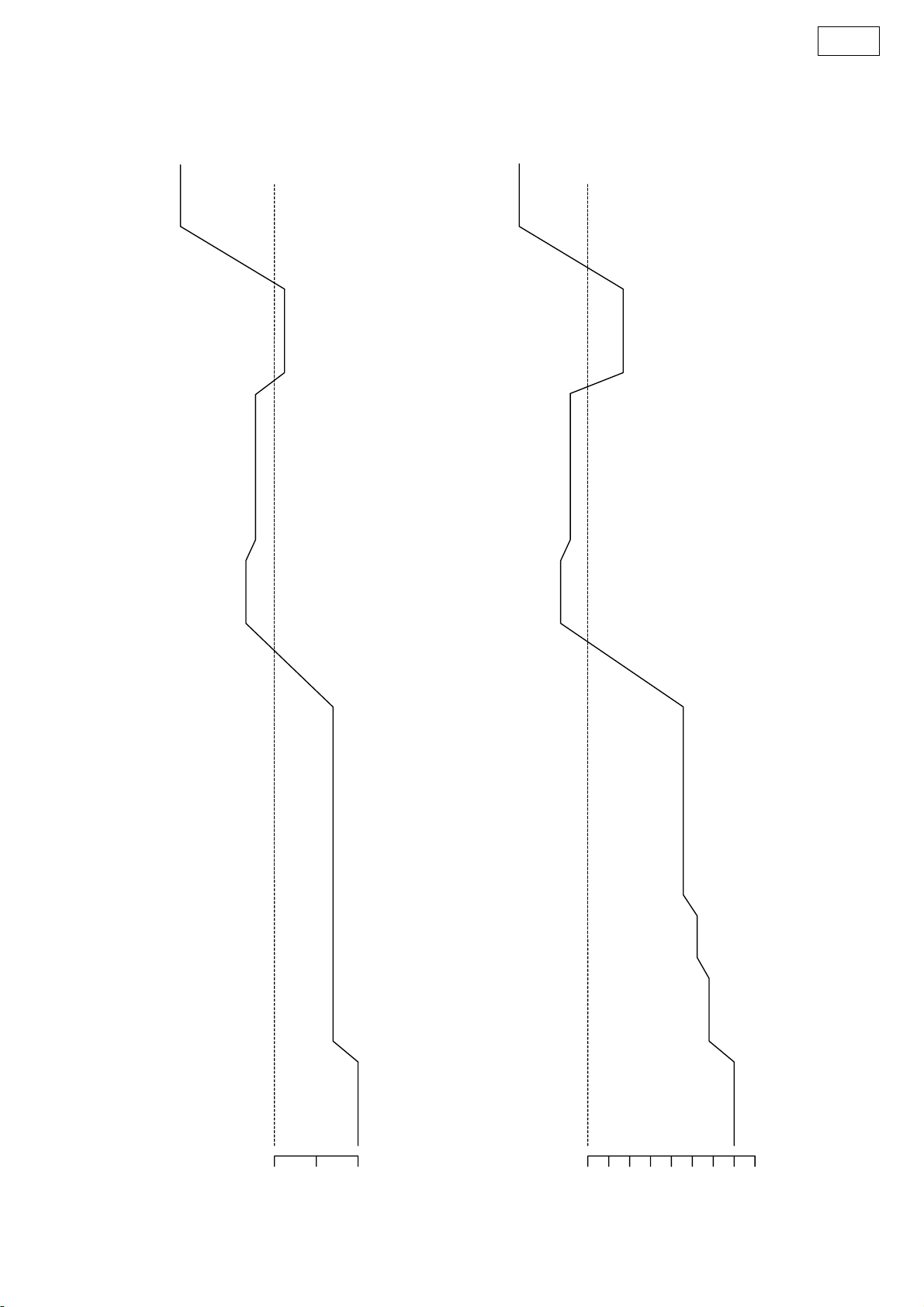
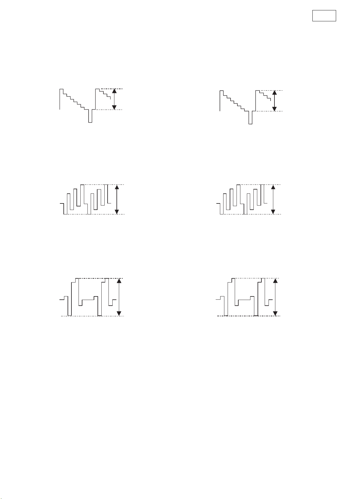
LEVEL DIAGRAM
S-301
㪂㪉㪋㪅㪐㪻㪙
㪄㪍㪅㪐㪻㪙
㪄㪉㪅㪊㪻㪙
㪂㪉㪇㪅㪏㪊㪻㪙
㪂㪉㪋㪅㪐㪻㪙
㪄㪈㪉㪅㪍㪻㪙
㪄㪉㪅㪊㪻㪙
㪂㪉㪐㪅㪊㪌㪻㪙
㪂㪊㪅㪊㪈㪻㪙
㪂㪉㪅㪏㪌㪻㪙
㪫㫆㫋㪸㫃㩷㪂㪊㪍㪅㪌㪉㪻㪙
㪂㪍㪻㪙
㪇㪻㪙㪝㫊
㪄㪈㪇㪻㪙㪝㫊
㪝㫉㫆㫅㫋㪄㪺㪿
㪄㪉㪇㪻㪙㪝㫊
㪇㪻㪙㪝㫊
㪄㪈㪇㪻㪙㪝㫊
㪪㪮㪄㪺㪿
㪄㪉㪇㪻㪙㪝㫊
㪂㪍㪻㪙
㪄㪊㪇㪻㪙㪝㫊
㪄㪋㪇㪻㪙㪝㫊
15
Page 16
SEMICONDUCTORS / 半導体一覧表
Only major semiconductors are shown, general semiconductors etc. are omitted to list.
主な半導体を記載しています。汎用の半導体は記載を省略しています。
1. IC’s
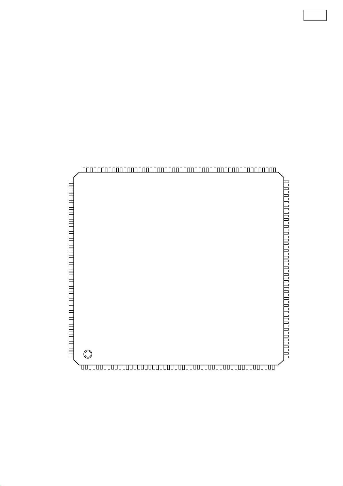
ES6138F (IC101: 1U-3692)
PINOUT DIAGRAM
HCS3FX#/AUX3[6]
VEE
/AUX4[4]
HA2
I2CDATA/AUX[0]
I2C_CLK/AUX[1]
VEE
AUX[2]/IOW#
VSS
VEE
AUX[3]/IOR#
AUX[4]
AUX[5]
AUX[6]
AUX[7]
LOE#
VSS
VCC
LCS0#
LCS1#
LCS2#
LCS3#
VSS
LD0
LD1
LD2
LD3
LD4
VEE
VSS
LD5
LD6
LD7
LD8
LD9
LD10
LD11
VSS
VEE
LD12
LD13
LD14
LD15
LWRLL#
LWR HL#
VSS
VEE
CAMIN0
CAMIN1
LA0
LA1
LA2
LA3
VSS
HCS1FX#/AUX3[7]
HA1/AUX4[3]
VSS
HA0/AUX4[2]
152
153
154
155
156
157
158
159
160
161
162
163
164
165
166
167
168
169
170
171
172
173
174
175
176
177
178
179
180
181
182
183
184
185
186
187
188
189
190
191
192
193
194
195
196
197
198
199
200
201
202
203
204
205
206
207
208
1
2 3 4 5 6 7 8 910111213141516171819202122232425262728293031323334353637383940414243444546474849505152
VSS
HIORDY/AUX3[3]
HIOCS16#/CAMCLK/AUX3[4]
HRD#/DCI_ACK#/AUX4[6]
150
151
HRST#/AUX3[5]
HWR#/DCI_CLK/AUX4[5]
VEE
145
146
147
148
149
HIRQ/DCI_ERR#/AUX4[7]
144
HRRQ#/AUX4[0]
143
HWRQ#/DCI_REQ#/AUX4[1]
142
HD15/AUX2[7]/IR
HD14/AUX2[6]
VCC
139
140
141
VSS
HD13/AUX2[5]/SP
HD12/AUX2[4]/C2PO
HD11/AUX2[3]//IRQ
135
136
137
138
ES6138F
HD10/AUX2[2]
HD9/AUX2[1]
HD8/DCI_FDS#/AUX2[0]/VFD_CLK
HD7/DCI7/AUX1[7]/VFD_DIN
131
132
133
134
VEE
130
VSS
129
HD6/DCI6/AUX1[6]/VFD_DOUT
128
HD5/DCI5/AUX1[5]
127
HD4/DCI4/AUX1[4]
126
HD3/DCI3/AUX1[3]
125
HD2/DCI2/AUX1[2]
124
HD1/DCI1/AUX1[1]
123
HD0/DCI0/AUX1[0]
122
VCC
121
VSS
120
HSYNC#/CAMIN7/AUX3[0]
119
VSYNC#/CAMIN6/AUX3[1]
118
PCLKQSCN/CAMIN5/AUX3[2]
117
PCLK2XSCN/CAMIN4
116
YUV7/FDAC/CAMIN3
YUV6/VDAC
YUV5/YDAC
ADVSS
112
113
114
115
ADVEE
YUV4/RSET
YUV3/COMP
YUV2/CDAC
108
109
110
111
YUV1/VREF
YUV0/CAMIN2/UDAC
DCLK
105
106
107
104
VEE
103
VSS
102
DSCK
101
DQM
100
DCS0#
99
VEE
98
VSS
97
DCS1#
96
DB15
95
DB14
94
DB13
93
DB12
92
VEE
91
VSS
90
DB11
89
DB10
88
DB9
87
DB8
86
DB7
85
DB6
84
VSS
83
VCC
82
DB5
81
DB4
80
DB3
79
DB2
78
DB1
77
DB0
76
VSS
75
VEE
74
DMBS1
73
DMBS0
72
DRAS#
71
DWE#
70
DOE#/DSCK_EN
69
DCAS#
68
VEE
67
VSS
66
DMA11
65
DMA10
64
DMA9
63
DMA8
62
DMA7
61
DMA6
60
VSS
59
VEE
58
DMA5
57
DMA4
56
DMA3
55
DMA2
54
DMA1
53
DMA0
S-301
NC
LA4
LA5
LA6
LA7
LA8
VEE
LA9
VSS
VCC
LA11
LA10
LA12
VSS
VEE
LA13
LA14
LA15
LA16
LA20
LA17
LA18
LA19
LA21
RESET#
TDMDX/RSEL
VEE
VSS
TDMDR
TDMCLK
VSS
VCC
TSD3
TDMFS
TDMTSC#
TWS/SEL_PLL2
TSD2
TSD0/SEL_PLL0
TSD1/SEL_PLL1
TBCK
MCLK
SPDIF_IN
SEL_PLL3/SPDIF_OUT
VSS
VCC
RSD
RWS
RBCK
XIN
AVE E
XOUT
AVS S
16
Page 17
ES6138F Pin Description
Name Pin Numbers I/O Definition
VEE 1,18, 27, 59, 68, 75,
92, 99, 104, 130,
148, 157, 159, 164,
183, 193, 201
P I/O power supply.
S-301
LA[21:0]
VSS 8, 17, 26, 34, 43,
VCC
RESET# 24 I Reset input (active-low).
TDMDX
RSEL I LCS3 ROM Boot Data Width Select. Strapped to VCC or ground via 4.7-kΩ
TDMDR 28 I TDM receive data input.
TDMCLK 29 I TDM clock input.
TDMFS 30 I TDM frame sync input.
2:7, 10:16, 19:23,
204:207
60, 67, 76, 84, 91,
98, 103, 120, 129,
138, 147, 156, 163,
171, 177, 184, 192,
200, 208
9, 35, 44, 83, 121,
139, 172
25
O RISC port address bus.
G Ground.
P Core power supply.
O TDM transmit data output.
resistor; read only during reset.
RSEL Selection
0 16-bit ROM
1 8-bit ROM
TDMTSC# 31 O TDM output enable (active-low).
TWS
SEL_PLL2 I System and DSCK output clock frequency selection is made at the rising edge of
32
O Audio transmit frame sync output.
RESET#. The matrix below lists the available clock frequencies and their
respective PLL bit settings. Strapped to VCC or ground via 4.7-kΩ resistor; read
only during reset.
SEL_PLL2 SEL_PLL1 SEL_PLL0 PLL Settings
0 0 0 DCLK × 4.5
001DCLK × 5.0
0 1 0 Bypass
011DCLK × 4.0
1 0 0 DCLK × 4.25
1 0 1 DCLK × 4.75
110DCLK × 5.5
111DCLK × 6.0
17
Page 18
p( )
Name Pin Numbers I/O Definition
S-301
TSD0
SEL_PLL0 I Refer to the description and matrix for SEL_PLL2 pin 32.
TSD1
SEL_PLL1 I Refer to the description and matrix for SEL_PLL2 pin 32.
TSD2 37 O Audio transmit serial data output 2.
TSD3 38 O Audio transmit serial data output 3.
NC 48 — No connect pins. Leave open.
MCLK 39 I/O Audio master clock for audio DAC.
TBCK 40 O Audio transmit bit clock.
SEL_PLL3
SPDIF_OUT O S/PDIF output.
SPDIF_IN 42 I S/PDIF input.
33
36
41
O Audio transmit serial data port 0.
O Audio transmit serial data port 1.
I Clock source select. Strapped to VCC or ground via 4.7-kΩ resistor; read only
during reset.
SEL_PLL3 Clock Source
0 Crystal oscillator
1 DCLK input
RSD 45 I Audio receive serial data.
RWS 46 I Audio receive frame sync.
RBCK 47 I Audio receive bit clock.
XIN 49 I 27-MHz crystal input.
XOUT 50 O 27-MHz crystal output.
AVEE 51 P Analog power for PLL.
AVSS 52 G Analog ground for PLL.
DMA[11:0] 53:58, 61:66 O DRAM address bus.
DCAS# 69 O DRAM column address strobe.
DOE#
70
DSCK_EN O DRAM clock enable.
DWE# 71 O DRAM write enable (active-low).
DRAS# 72 O DRAM row address strobe (active-low).
DMBS0 73 O DRAM bank select 0.
DMBS1 74 O DRAM bank select 1.
DB[15:0] 77:82, 85:90, 93:96 I/O DRAM data bus.
DCS[1:0]# 97,100 O DRAM chip select (active-low).
O DRAM output enable (active-low).
DQM 101 O Data input/output mask.
18
Page 19
p( )
Name Pin Numbers I/O Definition
DSCK 102 O Output clock to DRAM.
DCLK 105 I Clock input to PLL.
S-301
YUV0
CAMIN2 I Camera YUV 2.
UDAC O Video DAC output.
106
O YUV pixel 2 output data.
Pin 115 114 11 3 108 106
Value F DAC V DAC Y DAC C DAC U DAC
0 CVBS/Chroma CVBS1 Y C N/A
1 CVBS/Chroma CVBS1 Y C CVBS2
2 CVBS/Chroma N/A Y C N/A
3 CVBS/Chroma CVBS1 N/A N/A CVBS2
4 CVBS/Chroma CVBS1 N/A N/A N/A
5 CVBS/Chroma CVBS1 Y Pb Pr
6 CVBS/Chroma N/A Y Pb Pr
7 N/A SYNC G B R
8 CVBS/Chroma Chroma Y Pb Pr
9 CVBS CVBS1 G B R
10 CVBS CVBS1 G R B
11 N/A SYNC G R B
12 CVBS/Chroma N/A Y Pr Pb
13 CVBS/Chroma CVBS1 Y Pr Pb
14 Chroma Y G R B
F: CVBS/chroma signal for simultaneous mode.
Y: Luma component for YUV and Y/C processing.
C: Chrominance signal for Y/C processing.
U: Chrominance component signal for YUV mode.
V: Chrominance component signal for YUV mode.
YUV1
107
VREF I Internal voltage reference to video DAC. Bypass to ground with 0.1-µF capacitor.
YUV2
108
CDAC O Video DAC output. Refer to description and matrix for UDAC pin 106.
YUV3
109
COMP I Compensation input. Bypass to ADVEE with 0.1-µF capacitor.
YUV4
110
RSET I DAC current adjustment resistor input.
ADVEE 111 P Analog power for video DAC.
O YUV pixel 1 output data.
O YUV pixel 2 output data.
O YUV pixel 3 output data.
O YUV pixel 4 output data.
19
Page 20
p( )
Name Pin Numbers I/O Definition
ADVSS 112 G Analog ground for video DAC.
S-301
YUV5
YDAC O Video DAC output. Refer to description and matrix for UDAC pin 106.
YUV6
VDAC O Video DAC output. Refer to description and matrix for UDAC pin 106.
YUV7
FDAC O Video DAC output. Refer to description and matrix for UDAC pin 106.
CAMIN3 I Camera YUV 3.
PCLK2XSCN
CAMIN4 I Camera YUV 4.
PCLKQSCN
CAMIN5 I Camera YUV 5.
AUX3[2] I/O Aux3 data I/O.
VSYNC#
CAMIN6 I Camera YUV 6.
AUX3[1] I/O Aux3 data I/O.
HSYNC#
CAMIN7 I Camera YUV 7.
113
114
115
116
117
118
119
O YUV pixel 5 output data.
O YUV pixel 6 output data.
O YUV pixel 7 output data.
I/O 27-MHz video output pixel clock.
O 13.5-MHz video output pixel clock.
I/O Vertical sync (active-low).
I/O Horizontal sync (active-low).
AUX3[0] I/O Aux3 data I/O.
HD[5:0]
DCI[5:0] I/O DVD channel data I/O.
AUX1[5:0] I/O Aux1 data I/O.
HD6
DCI6 I/O DVD channel data I/O.
AUX1[6] I/O Aux1 data I/O.
VFD_DOUT I VFD data output.
HD7
DCI7 I/O DVD channel data I/O.
AUX1[7] I/O Aux1 data I/O.
VFD_DIN I VFD data input.
HD8
DCI_FDS# I/O DVD input sector start (active-low).
AUX2[0] I/O Aux2 data I/O.
VFD_CLK I VFD clock input.
122:127
128
131
132
I/O Host data bus lines 5:0.
I/O Host data bus line 6.
I/O Host data bus line 7.
I/O Host data bus line 8.
20
Page 21
p( )
Name Pin Numbers I/O Definition
S-301
HD9
AUX2[1] I/O Aux2 data I/O.
HD10
AUX2[2] I/O Aux2 data I/O.
HD11
AUX2[3] I/O Aux2 data I/O.
IRQ O IRQ.
HD12
AUX2[4] I/O Aux2 data I/O.
C2PO I C2PO error correction flag from CD-ROM.
HD13
AUX2[5] I/O Aux2 data I/O.
SP I 16550 UART serial port input.
HD14
AUX2[6] I/O Aux2 data I/O.
HD15
AUX2[7] I/O Aux2 data I/O.
133
134
135
136
137
140
141
I/O Host data bus line 9.
I/O Host data bus line 10.
I/O Host data bus line 11.
I/O Host data bus line 12.
I/O Host data bus line 13.
I/O Host data bus line 14.
I/O Host data bus line 15.
IR I IR remote control input.
HWRQ#
DCI_REQ# O DVD control interface request (active-low).
AUX4[1] I/O Aux4 data I/O.
HRRQ#
AUX4[0] I/O Aux4 data I/O.
HIRQ
DCI_ERR# I/O DVD channel data error (active-low).
AUX4[7] I/O Aux4 data I/O.
HRST#
AUX3[5] I/O Aux3 data I/O.
HIORDY
AUX3[3] I/O Aux3 data I/O.
HWR#
DCI_CLK I/O DVD channel data clock.
AUX4[5] I/O Aux4 data I/O.
142
143
144
145
146
149
O Host write request (active-low).
O Host read request (active-low).
I/O Host interrupt.
O Host reset (active-low).
I Host I/O ready.
I/O Host write (active-low).
21
Page 22
p( )
Name Pin Numbers I/O Definition
S-301
HRD#
DCI_ACK# O DVD channel data valid (active-low).
150
O Host read (active-low).
AUX4[6] I/O Aux4 data I/O.
HIOCS16#
CAMCLK I Camera port pixel clock input.
151
I Device 16-bit data transfer (active-low).
AUX3[4] I/O Aux3 data I/O.
HCS1FX#
O Host select 1 (active-low).
152
AUX3[7] I/O Aux3 data I/O.
HCS3FX#
O Host select 3 (active-low).
153
AUX3[6] I/O Aux3 data I/O.
HA[2:0]
I/O Host address bus.
154, 155, 158
AUX4[4:2] I/O Aux4 data I/Os.
AUX[0]
160
I2CDATA I/O I
AUX[1]
161
I2C_CLK I/O I
AUX[2]
I/O Auxiliary port 0 (open collector).
2
C data I/O.
I/O Auxiliary port 1 (open collector).
2
C clock I/O.
I/O Auxiliary port.
162
IOW# O I/O write strobe (LCS1) (active-low).
AUX[3]
I/O Auxiliary port.
165
IOR# O I/O read strobe (LCS1) (active-low).
AUX[6:4] 166:168 I/O Auxiliary ports.
AUX[7] 169 I/O Auxiliary port.
LOE# 170 O RISC port output enable (active-low).
LCS[3:0]# 173:176 O RISC port chip select (active-low).
LD[15:0]
178:182,
185:191,194:197
I/O RISC port data bus.
LWRLL# 198 O RISC port low-byte write enable (active-low).
LWRHL# 199 O RISC port high-byte write enable (active-low).
CAMIN0 202 I Camera YUV 0.
CAMIN1 203 I Camera YUV 1.
22
Page 23
FLI2310 (IC403: 1U-3692)
t
Pin Diagram
FIELD ID_PORT2
HSYNC_PORT2
VSYNC_PORT2
D1_IN_7
D1_IN_6
D1_IN_5
S-301
R_VDD
IN_CLK_PORT2
XTAL IN
XTAL OUT
VDD9
VSS
D1_IN_4
D1_IN_3
D1_IN_0
D1_IN_2
D1_IN_1
VDDcore8
VSScore
TEST0
TEST1
TEST2
R_VDD
R_VSS
R_VSS
R_VDD
R_VSS
R_VDD
R_VDD
R_VSS
Reserved
Reserved
Reserved
R_VSS
R_VSS
Reserved
Reserved
R_VSS
AVDD_PLL_FE
R_VDD1.8
AVDD_PLL_SDI
AVSS_PLL_BE2
AVSS_PLL_FE
AVSS_PLL_SDI
PLL_PVDD
AVDD_PLL_BE2
PLL_PVSS
AVSS_PLL_BE1
AVDD_PLL_BE1
R_VSS
R_VDD
Reserved
HSYNC1_PORT1
VSYNC1_PORT1
FIELD ID1_PORT1
IN_CLK1_PORT1
HSYNC2_PORT1
VSYNC2_PORT1
FIELD ID2_PORT1
VDD1
VSS
IN_CLK2_PORT1
B/Cb/D1_0
B/Cb/D1_1
B/Cb/D1_2
B/Cb/D1_3
B/Cb/D1_4
VDDcore1
VSScore
B/Cb/D1_5
B/Cb/D1_6
B/Cb/D1_7
R/Cr/Cb Cr_0
R/Cr/Cb Cr_1
R/Cr/Cb Cr_2
R/Cr/Cb Cr_3
R/Cr/Cb Cr_4
R/Cr/Cb Cr_5
R/Cr/Cb Cr_6
R/Cr/Cb Cr_7
G/Y/Y_0
VDD2
VSS
G/Y/Y_1
G/Y/Y_2
G/Y/Y_3
G/Y/Y_4
VDDcore2
VSScore
G/Y/Y_5
G/Y/Y_6
G/Y/Y_7
IN_SEL
TEST
DEV_ADDR1
DEV_ADDR0
SCLK
SDATA
RESET_N
VDD3
SDRAM DATA(0)
SDRAM DATA(1)
SDRAM DATA(2)
VSS
1 0 0
1 6 0
1 5 5
1 5 0
1 4 5
1 4 0
1 3 5
1 3 0
1 2 5
1 2 0
1 1 5
1 1 0
1 0 5
OE
G/Y/Y_OUT_7
G/Y/Y_OUT_6
G/Y/Y_OUT_5
G/Y/Y_OUT_4
G/Y/Y_OUT_3
G/Y/Y_OUT_2
G/Y/Y_OUT_1
G/Y/Y_OUT_0
VSS
VDD8
R/V/Pr_OUT_7
R/V/Pr_OUT_6
R/V/Pr_OUT_5
R/V/Pr_OUT_4
R/V/Pr_OUT_3
R/V/Pr_OUT_2
VSScore
VDDcore7
R/V/Pr_OUT_1
R/V/Pr_OUT_0
B/U/Pb_OUT_7
B/U/Pb_OUT_6
B/U/Pb_OUT_5
B/U/Pb_OUT_4
B/U/Pb_OUT_3
B/U/Pb_OUT_2
VSS
VDD7
B/U/Pb_OUT_1
B/U/Pb_OUT_0
CLKOUT
VSScore
VDDcore6
CTLOUT4
CTLOUT3
CTLOUT2
CTLOUT1
CTLOUT0
TEST OUT1
TEST OUT0
TEST3
SDRAM CLKIN
VSS
VDD6
SDRAM CLKOUT
SDRAM DQM
SDRAM CSN
SDRAM BA0
SDRAM BA1
SDRAM CASN
SDRAM RASN
2 0 5
1
2 0 0
1 9 5
1 9 0
1 8 5
1 8 0
1 7 5
1 7 0
1 6 5
5
1 0
1 5
2 0
2 5
3 0
3 5
4 0
4 5
5 0
5 5
6 0
6 5
7 0
7 5
8 0
8 5
9 0
9 5
Block Diagrams
Port 2
8-bit
656 Input
Port 1
8/16/24-bit
RGB/YCrCb
Input
Input Processor
with Auto Sync
and auto Adjust
Generation
SDRAM DATA(3)
Clock
PLLs
VSS
VDD4
SDRAM DATA(5)
SDRAM DATA(4)
SDRAM DATA(8)
SDRAM DATA(7)
SDRAM DATA(6)
SDRAM DATA(9)
SDRAM DATA(10)
SDRAM DATA(12)
SDRAM DATA(11)
Noise Reducer,
Deinterlacer, Frame
Rate Converter and
SDRAM interface
VSScore
VDDcore3
SDRAM DATA(21)
SDRAM DATA(17)
SDRAM DATA(16)
SDRAM DATA(14)
SDRAM DATA(13)
SDRAM DATA(15)
SDRAM DATA(18)
SDRAM DATA(22)
SDRAM DATA(20)
SDRAM DATA(19)
SDRAM DATA(24)
SDRAM DATA(23)
SDRAM DATA(25)
VSScore
VDDcore4
SDRAM DATA(28)
SDRAM DATA(26)
SDRAM DATA(27)
Vertical and
Horizontal
Scalers
VSS
VDD5
TEST IN
SDRAM DATA(31)
SDRAM DATA(30)
SDRAM DATA(29)
SDRAM ADDR(9)
SDRAM ADDR(10)
SDRAM ADDR(7)
SDRAM ADDR(8)
SDRAM ADDR(6)
VSScore
VDDcore5
SDRAM ADDR(5)
SDRAM ADDR(4)
SDRAM ADDR(3)
SDRAM ADDR(2)
SDRAM ADDR(0)
SDRAM ADDR(1)
SDRAM WEN
Output
Processor
16/20/24-bi
RBG/YCrCb
Digital Outputs
2Mx32
SDRAM
(external)
Vertical and
Horizontal
Enhancers
23
Page 24
Pin details
S-301
Pin
No Pin Name I/O Type
1
HSYNC1_PORT1 Input 5v
2
VSYNC1_PORT1 Input 5v
FIELD ID1_PORT1
3
IN_CLK1_PORT1
4
5
HSYNC2_PORT1 Input 5v
6
VSYNC2_PORT1 Input 5v
FIELD ID2_PORT1
7
VDD1
8
VSS
9
IN_CLK2_PORT1
10
B/Cb/D1_0
11
B/Cb/D1_1
12
B/Cb/D1_2
13
B/Cb/D1_3
14
B/Cb/D1_4
15
VDDcore1
16
VSScore
17
B/Cb/D1_5
18
B/Cb/D1_6
19
B/Cb/D1_7
20
R/Cr/Cb Cr_0
21
R/Cr/Cb Cr_1
22
R/Cr/Cb Cr_2
23
R/Cr/Cb Cr_3
24
R/Cr/Cb Cr_4
25
R/Cr/Cb Cr_5
26
R/Cr/Cb Cr_6
27
R/Cr/Cb Cr_7
28
G/Y/Y_0
29
VDD2
30
VSS
31
G/Y/Y_1
32
G/Y/Y_2
33
G/Y/Y_3
34
G/Y/Y_4
35
VDDcore2
36
VSScore
37
G/Y/Y_5
38
G/Y/Y_6
39
G/Y/Y_7
40
41
IN_SEL Output 5v 8 mA
42 TEST Input 5v
43
DEV_ADDR1 Input 5v
44
DEV_ADDR0 Input 5v
Input 5v
Input 5v
Input 5v
Power 3.3 V - Power pin for IO
Ground Ground
Input 5v
Input 5v
Input 5v
Input 5v
Input 5v
Input 5v
Power 1.8 V - Power pin for core
Ground Ground
Input 5v
Input 5v
Input 5v
Input 5v
Input 5v
Input 5v
Input 5v
Input 5v
Input 5v
Input 5v
Input 5v
Input 5v
Power 3.3 V - Power pin for IO
Ground Ground
Input 5v
Input 5v
Input 5v
Input 5v
Power 1.8 V - Power pin for core
Ground Ground
Input 5v
Input 5v
Input 5v
Voltage
Tolerance Drive
Pull up/
Pulldown Description
Horizontal sync or reference -CTL1 of Port 1
Vertical sync or reference -CTL1 of Port 1
Odd/Even Field identification -CTL1 of Port 1
Data Clock input -CTL1 of Port 1
Horizontal sync or reference –CTL2 of Port 1
Vertical sync or reference –CTL2 of Port 1
Odd/Even Field identification –CTL2 of Port 1
Data Clock input –CTL2 of Port 1
Port 1 – Digital video input (Blue/Cb/D1)
Port 1 – Digital video input (Blue/Cb/D1)
Port 1 – Digital video input (Blue/Cb/D1)
Port 1 – Digital video input (Blue/Cb/D1)
Port 1 – Digital video input (Blue/Cb/D1)
Port 1 – Digital video input (Blue/Cb/D1)
Port 1 – Digital video input (Blue/Cb/D1)
Port 1 – Digital video input (Blue/Cb/D1)
Port 1 – Digital video input (Red/Cr/CrCb)
Port 1 – Digital video input (Red/Cr/CrCb)
Port 1 – Digital video input (Red/Cr/CrCb)
Port 1 – Digital video input (Red/Cr/CrCb)
Port 1 – Digital video input (Red/Cr/CrCb)
Port 1 – Digital video input (Red/Cr/CrCb)
Port 1 – Digital video input (Red/Cr/CrCb)
Port 1 – Digital video input (Red/Cr/CrCb)
Port 1 – Digital video input (Green/Y)
Port 1 – Digital video input (Green/Y)
Port 1 – Digital video input (Green/Y)
Port 1 – Digital video input (Green/Y)
Port 1 – Digital video input (Green/Y)
Port 1 – Digital video input (Green/Y)
Port 1 – Digital video input (Green/Y)
Port 1 – Digital video input (Green/Y)
Output to select external video mux
Connect to Ground
Device address setting 1
Device address setting 0
24
Page 25
S-301
Pin
No Pin Name I/O Type
45 SCLK
46 SDATA
47 RESET_N
48 VDD3
49 VSScore
50 SDRAM DATA(0)
51 SDRAM DATA(1)
52 SDRAM DATA(2)
53 SDRAM DATA(3)
54 SDRAM DATA(4)
55 SDRAM DATA(5)
56 SDRAM DATA(6)
57 SDRAM DATA(7)
58 SDRAM DATA(8)
59 SDRAM DATA(9)
60 SDRAM DATA(10)
61 SDRAM DATA(11)
62 VDD4
63 VSS
64 SDRAM DATA(12)
65 SDRAM DATA(13)
66 SDRAM DATA(14)
67 SDRAM DATA(15)
68 VDDcore3
69 VSScore
70 SDRAM DATA(16)
71 SDRAM DATA(17)
72 SDRAM DATA(18)
73 SDRAM DATA(19)
74 SDRAM DATA(20)
75 SDRAM DATA(21)
76 SDRAM DATA(22)
77 SDRAM DATA(23)
78 SDRAM DATA(24)
79 SDRAM DATA(25)
80 VDDcore4
81 VSScore
82 SDRAM DATA(26)
83 SDRAM DATA(27)
84 SDRAM DATA(28)
85 SDRAM DATA(29)
86 SDRAM DATA(30)
87 SDRAM DATA(31)
88 VDD5
I/O
I/O
Input
Power
Ground
Tristate I/O
Tristate I/O
Tristate I/O
Tristate I/O
Tristate I/O
Tristate I/O
Tristate I/O
Tristate I/O
Tristate I/O
Tristate I/O
Tristate I/O
Tristate I/O
Power
Ground
Tristate I/O
Tristate I/O
Tristate I/O
Tristate I/O
Power
Ground
Tristate I/O
Tristate I/O
Tristate I/O
Tristate I/O
Tristate I/O
Tristate I/O
Tristate I/O
Tristate I/O
Tristate I/O
Tristate I/O
Power
Ground
Tristate I/O
Tristate I/O
Tristate I/O
Tristate I/O
Tristate I/O
Tristate I/O
Power
Voltage
Tolerance Drive
5v 8 mA 2-wire serial control bus clock
5v 8 mA 2-wire serial control bus data
5v PU Reset
3.3 V – Power pin for IO
Ground
5v 4 mA PD
5v 4 mA PD
5v 4 mA PD
5v 4 mA PD
5v 4 mA PD
5v 4 mA PD
5v 4 mA PD
5v 4 mA PD
5v 4 mA PD
5v 4 mA PD
5v 4 mA PD
5v 4 mA PD
3.3 V – Power pin for IO
Ground
5v 4 mA PD
5v 4 mA PD
5v 4 mA PD
5v 4 mA PD
1.8 V - Power pin for core
Ground
5v 4 mA PD
5v 4 mA PD
5v 4 mA PD
5v 4 mA PD
5v 4 mA PD
5v 4 mA PD
5v 4 mA PD
5v 4 mA PD
5v 4 mA PD
5v 4 mA PD
1.8 V – Power pin for core
Ground
5v 4 mA PD SDRAM data bus *
5v 4 mA PD
5v 4 mA PD
5v 4 mA PD
5v 4 mA PD
5v 4 mA PD
3.3 V – Power pin for IO
Pull up/
Pulldown Description
SDRAM data bus *
SDRAM data bus *
SDRAM data bus *
SDRAM data bus *
SDRAM data bus *
SDRAM data bus *
SDRAM data bus *
SDRAM data bus *
SDRAM data bus *
SDRAM data bus *
SDRAM data bus *
SDRAM data bus *
SDRAM data bus *
SDRAM data bus *
SDRAM data bus *
SDRAM data bus *
SDRAM data bus *
SDRAM data bus *
SDRAM data bus *
SDRAM data bus *
SDRAM data bus *
SDRAM data bus *
SDRAM data bus *
SDRAM data bus *
SDRAM data bus *
SDRAM data bus *
SDRAM data bus *
SDRAM data bus *
SDRAM data bus *
SDRAM data bus *
SDRAM data bus *
25
Page 26
S-301
Pin
No Pin Name I/O Type
89 VSS
90 TEST IN
91 SDRAM ADDR(10)
92 SDRAM ADDR(9)
93 SDRAM ADDR(8)
94 SDRAM ADDR(7)
95 SDRAM ADDR(6)
96 VDDcore5
97 VSScore
98 SDRAM ADDR(5)
99 SDRAM ADDR(4)
100 SDRAM ADDR(3)
101 SDRAM ADDR(2)
102 SDRAM ADDR(1)
103 SDRAM ADDR(0)
104 SDRAM WEN
105 SDRAM RASN
106 SDRAM CASN
107 SDRAM BA1
108 SDRAM BA0
109 SDRAM CSN
110 SDRAM DQM
111 SDRAM CLKOUT
112 VDD6
113 VSS
114 SDRAM CLKIN
115 TEST3
116 TEST OUT0
TEST OUT1 / Interrupt
117
Out Output
118 CTLOUT0
119 CTLOUT1
120 CTLOUT2
121 CTLOUT3
122 CTLOUT4
123 VDDcore6
124 VSScore
125 CLKOUT
126 B/U/Pb_OUT_0
127 B/U/Pb_OUT_1
Ground
Input
Tristate O/P
Tristate O/P
Tristate O/P
Tristate O/P
Tristate O/P
Power
Ground
Tristate O/P
Tristate O/P
Tristate O/P
Tristate O/P
Tristate O/P
Tristate O/P
Tristate O/P
Tristate O/P
Tristate O/P
Tristate O/P
Tristate O/P
Tristate O/P
Tristate O/P
Output
Power
Ground
Input
Input
Output
Tristate O/P
Tristate O/P
Tristate O/P
Tristate O/P
Tristate O/P
Power
Ground
Tristate O/P
Tristate O/P
Tristate O/P
Voltage
Tolerance Drive
Ground
5V Test input-Connect to ground
5v 8 mA SDRAM address bus *
5v 8 mA SDRAM address bus *
5v 8 mA SDRAM address bus *
5v 8 mA SDRAM address bus *
5v 8 mA SDRAM address bus *
1.8 V – Power pin for core
Ground
5v 8 mA SDRAM address bus *
5v 8 mA SDRAM address bus *
5v 8 mA SDRAM address bus *
5v 8 mA SDRAM address bus *
5v 8 mA SDRAM address bus *
5v 8 mA SDRAM address bus *
5v 8 mA SDRAM write enable *
5v 8 mA SDRAM row address select *
5v 8 mA SDRAM column address select *
5v 8 mA SDRAM bank select 1*
5v 8 mA SDRAM bank select 0*
5v 4 mA SDRAM CS *
5v 8 mA SDRAM DQM *
5v 12 mA Clock out to SDRAM *
3.3 V - Power pin for IO
Ground
5v Trace delayed SDRAM Clock in
Test input – Connect to ground
Test output – leave open
Interrupt Output
5v 8 mA
5v 8 mA
5v 8 mA
5v 8 mA
5v 8 mA
1.8 V - Power pin for core
Ground
5v 12 mA Output data rate clock
5v 8 mA
5v 8 mA
Pull up/
Pulldown Description
Control signal output selectable as HSync1/
CSync/HRef/Monitor coast
Control signal output selectable as
VSync1/CRef/VRef/Film Indicator
Control signal output selectable as Monitor
coast/HRef/VDD_en / HSync2
Control signal output selectable as Film
Indicator/VRef/backlight_en/VSync2
Control signal output selectable as CRef/Field
ID/CSync/Monitor coast
Digital video output – Blue/U/Pb
Digital video output – Blue/U/Pb
26
Page 27
S-301
Pin
No
Pin Name I/O Type
128 VDD7
129 VSS
130 B/U/Pb_OUT_2
131 B/U/Pb_OUT_3
132 B/U/Pb_OUT_4
133 B/U/Pb_OUT_5
134 B/U/Pb_OUT_6
135 B/U/Pb_OUT_7
136 R/V/Pr_OUT_0
137 R/V/Pr_OUT_1
138 VDDcore7
139 VSScore
140 R/V/Pr_OUT_2
141 R/V/Pr_OUT_3
142 R/V/Pr_OUT_4
143 R/V/Pr_OUT_5
144 R/V/Pr_OUT_6
145 R/V/Pr_OUT_7
146 VDD8
147 VSS
148 G/Y/Y_OUT_0
G/Y/Y_OUT_1
149
G/Y/Y_OUT_2
150
G/Y/Y_OUT_3
151
G/Y/Y_OUT_4
152
G/Y/Y_OUT_5
153
G/Y/Y_OUT_6
154
G/Y/Y_OUT_7
155
156 OE
157 PLL_PVDD
158 PLL_PVSS
159 AVSS_PLL_BE1
160 AVDD_PLL_BE1
161 AVDD_PLL_BE2
162 AVSS_PLL_BE2
163 AVSS_PLL_SDI
164 AVDD_PLL_SDI
165 AVDD_PLL_FE
166 AVSS_PLL_FE
167 DAC_PVSS
168 DAC_VDD
169 DAC_VSS
170 DAC_BOUT
171
DAC_AVDDB
Power
Ground
Tristate O/P
Tristate O/P
Tristate O/P
Tristate O/P
Tristate O/P
Tristate O/P
Tristate O/P
Tristate O/P
Power
Ground
Tristate O/P
Tristate O/P
Tristate O/P
Tristate O/P
Tristate O/P
Tristate O/P
Power
Ground
Tristate O/P
Tristate O/P
Tristate O/P
Tristate O/P
Tristate O/P
Tristate O/P
Tristate O/P
Tristate O/P
Input
Power
Ground
Ground
Power
Power
Ground
Ground
Power
Power
Ground
Ground
Power
Ground
Output
Power
Voltage
Tolerance
3.3 V – Power pin for IO
Ground
5v 8 mA Digital video output – Blue/U/Pb
5v 8 mA
5v 8 mA
5v 8 mA
5v 8 mA
5v 8 mA
5v 8 mA Digital video output – Red/V/Pr
5v 8 mA Digital video output – Red/V/Pr
1.8 V – Power pin for core
Ground
5v 8 mA
5v 8 mA
5v 8 mA
5v 8 mA
5v 8 mA
5v 8 mA
3.3 V – Power pin for IO
Ground
5v 8 mA Digital video output – Green/Y
5v 8 mA
5v 8 mA
5v 8 mA
5v 8 mA
5v 8 mA
5v 8 mA
5v 8 mA
5v Output data enable for Digital video output
1.8 V – Power pin for PLL pads
Ground for PLL pads
PLL Ground
1.8 V – Power pin for PLL
1.8 V – Power pin for PLL
PLL Ground
PLL Ground
1.8 V – Power pin for PLL
1.8 V – Power pin for PLL
PLL Ground
Ground for DAC pads
1.8 V – Digital power pin for DAC
DAC digital Ground
34 mA Analog B/U output
3.3 V – Analog power pin for B channel
Drive
Pull up/
Pulldown
Description
Digital video output – Blue/U/Pb
Digital video output – Blue/U/Pb
Digital video output – Blue/U/Pb
Digital video output – Blue/U/Pb
Digital video output – Blue/U/Pb
Digital video output – Red/V/Pr
Digital video output – Red/V/Pr
Digital video output – Red/V/Pr
Digital video output – Red/V/Pr
Digital video output – Red/V/Pr
Digital video output – Red/V/Pr
Digital video output – Green/Y
Digital video output – Green/Y
Digital video output – Green/Y
Digital video output – Green/Y
Digital video output – Green/Y
Digital video output – Green/Y
Digital video output – Green/Y
27
Page 28
S-301
Pin
No
Pin Name I/O Type
172 DAC_AVSSB
173 DAC_GOUT
174 DAC_AVDDG
175 DAC_AVSSG
176 DAC_ROUT
177 DAC_AVDDR
178 DAC_AVSSR
179 DAC_COMP
180 DAC_RSET
181 DAC_VREFOUT
182 DAC_VREFIN
183 DAC_AVDD
184 DAC_AVSS
185 DAC_GR_AVSS
186 DAC_GR_AVDD
187 DAC_PVDD
188 TEST0
189 TEST1
190 TEST2
191 XTAL IN
192 XTAL OUT
193 VDD9
194 VSS
195 IN_CLK_PORT 2
196 D1_IN_0
197 VDDcore8
198 VSScore Ground Ground
199 D1_IN_1 Input 5v 4 mA Port 2 - ITU-R BT656 digital data input
200 D1_IN_2 Input 5v 4 mA Port 2 - ITU-R BT656 digital data input
201 D1_IN_3 Input 5v 4 mA Port 2 - ITU-R BT656 digital data input
202 D1_IN_4 Input 5v 4 mA Port 2 - ITU-R BT656 digital data input
203 D1_IN_5 Input 5v 4 mA Port 2 - ITU-R BT656 digital data input
204 D1_IN_6 Input 5v 4 mA Port 2 - ITU-R BT656 digital data input
205 D1_IN_7 Input 5v 4 mA Port 2 - ITU-R BT656 digital data input
206 FIELD ID_PORT 2
207 VSYNC_ PORT 2
208 HSYNC_PORT 2
Ground
Output
Power
Ground
Output
Power
Ground
Output
Output
Output
Input
Power
Ground
Ground
Power
Power
Input
Input
Input
Input
Output
Power
Ground
Input
Input
Power
Input
Input
Input
Voltage
Tolerance
Analog Ground for B channel
34 mA Analog G/Y output
3.3 V – Analog power pin for G channel
Analog Ground for G channel
34 mA Analog R/V output
3.3 V – Analog power pin for R channel
Analog Ground for R channel
Compensation for video DACs
Current setting resistor for video DACs
External Voltage reference for video DACs
3.3 V – Analog power pin for DAC
Analog Ground for DAC
Ground for DAC Guard ring
3.3 V – Power pin for DAC Guard ring
3.3 V –Power pin for DAC pads
5v Test pin – connect to ground
5v Test pin – connect to ground
5v Test pin – connect to ground
External parallel crystal oscillator
External parallel crystal oscillator
3.3 V - Power pin for IO
Ground
5v 4 mA Port 2 - Data Clock input
5v 4 mA Port 2 - ITU-R BT656 digital data input
1.8 V – Power pin for core
5v 4 mA Port 2 - Odd/Even Field identification
5v 4 mA Port 2 - Vertical sync or reference
5v 4 mA Port 2 - Horizontal sync or reference
Drive
Pull up/
Pulldown
Description
1.28 V Internally generated voltage reference for
video DACs
Note: * - The connection of these pins depends on the type of external SDRAM used.
28
Page 29
CXD1885Q (IC805: 1U-3692)
S-301
DRAM I/F PWM.FG D/A
DV
TEST10
TEST11
TEST12
TEST13
TEST14
TEST15
MODSEL0
MODSEL1
MODSEL2
DV
DV
General Port
JTAG Test/Monitor Pin
VMCHG
DVDD18
DD33
RD8
TEST0
TEST1
TEST2
TEST3
TEST4
TEST5
TEST6
TEST7
TEST8
TEST9
DV
GIO0
GIO1
GIO2
GIO3
DD33
GIO4
GIO5
GIO6
GIO7
DD18
GIO8
GIO9
GIO10
GIO11
GIO12
DV
GIO13
GIO14
GIO15
GIO16
GIO17
GIO18
GIO19
TRST
TMS
TCK
TDO
18
DD
DV
RD9
RD10
RD11
RD12
RD13
RD14
RD15
RD0
RD1
157
158
159
160
161
162
163
164
165
166
167
168
169
170
171
172
173
174
175
176
177
SS
178
179
180
181
182
183
184
185
186
187
188
189
190
191
192
193
194
SS
195
196
197
198
199
200
201
202
203
204
TDI
205
206
207
208
RD2
RD3
RD4
RD5
SS
RD6
DV
1 2 3 4 5 6 7 8 9 10 11 12 13 14 15 16 17 18 19 20 21 22 23 24 25 26 27 28 29 30 31 32 33 34 35 36 37 38 39 40 41 42 43 44 45 46 47 48 49 50 51 52
33
MA0
MA1
MA2
MA3
MA4
MA5
MA6
MA7
MA8
MD0
DD
ALCR
MSEL0
MSEL1
DV
MD1
TESTSEL
RD7
MD2
XMWR
MD3
XRAS
MD4
RA0
MD5
18
DD
DV
SS
DV
RA1
MD6
RA2
MD7
RA3
MALE
RA4
MCS
33
DD
DV
MWR
RA5
33
DD
DV
RA6
MRD
RA7
SS
RA10
RA11
XMOE
XUCAS
XLCAS
GPWM5
GPWM4
GPWM3
GPWM2
GPWM1
VDT5
VDT4
VDT3
VDT2
GPWM0
VDT1
RA8
RA9
DV
XI
SS
18
DD
MINT
MRDY
SYSCK
DV
SS
XO
DV
DV
VDT7
VDT6
SPWM2
SPWM1FGAVSSDA3 (SLED2_TILT)
VDT0
HDRQ
VSTEM I/FClockB/E MCU I/F
33
DD
DA2 (FSCON)
DA1 (SLED)
DA0 (TSCON)
AV
105106107108109110111112113114115116117118119120121122123124125126127128129130131132133134135136137138139140141142143144145146147148149150151152153154155156
AV
DD18
104
VREFL
103
VREFH
102
AD9
101
AD8
100
AD7
99
AD6
98
AD5
97
AD4
96
AD3
95
AV
94
AD2
93
AD1
92
AD0
91
AVSS
90
AV
89
RC
88
LPF2
87
LPF1
86
VCOI
85
AV
84
VFBC
83
CHG
82
JMOUT
81
JMREF
80
AV
79
IREF
78
TLC1
77
TLC0
76
HF
75
ATC
74
AV
73
DTC
72
MIRRORH
71
HFD
70
RFOKGH
69
SCLKH
68
SO
67
SI
66
CSL
65
EXPLDT
64
EXVCO
63
BCK
62
LRCK
61
DOTK
60
DADT
59
C2PO
58
DRVRDY
57
DRVCLK
56
DRVRX
55
DRVTX
54
DV
53
18
DCK
XSHD
DRVIRQ
DRVRST
DD
DV
VEFG
XHAC
A/DData PLL/Data SlicerASP S-I/O, Defect etcAudio D/AVSTEM I/F
DD33
SS
DD18
DD33
SS
DD33
29
Page 30
16/4M DRAM
S-301
HFD
HF
ASP
PWM
AT C
JTAG
Mecha
control
Servo
singnal
Data
Slicer
Data-PLL
ASP Serial I/F
TZC
GIO
A/D
TC
Direction
ROM/RAM
ICU Timer
BCA
DVD
Demodulation
CD-DSP (DDCD)
VSTEM
Serial I/F
Spindle
DSP
Data
RAM
D/A
PWM
CMD/
RSP
reg.
Memory
manager
CD-ROM
Header Dec.
Peri. CLK
Audio I/F
ECC Core
EDC
MPEG I/F
DSP CLK/Mode
MCU I/F
ICU
Video
Serial
Command
Audio
MCU
Servo
control
X'tal
VSTEM
Functions (A/D : Analog/Digital, PU : Pull-up, PD : Pull-down, SMT=Schumitt )
No. Terminal Name I/O A/D Classification Function PU PD SMT
DD33 P VDD & GND Digital 3.3V Power for I/O.
1DV
2 ALCR I D MCU I/F Chip select input. (L: Reset) * *
3 MSEL0 I D MCU I/F MCU I/F mode select 0. *
4 MSEL1 I D MCU I/F MCU I/F mode select 1. *
5 MA0 I/O D MCU I/F MCU Adress input 0 / data I/O 0 <LSB>. *
6 MA1 I/O D MCU I/F MCU Adress input 1 / data I/O 1. *
7 MA2 I/O D MCU I/F MCU Adress input 2 / data I/O 2. *
8 MA3 I/O D MCU I/F MCU Adress input 3 / data I/O 3. *
9 MA4 I/O D MCU I/F MCU Adress input 4 / data I/O 4. *
10 MA5 I/O D MCU I/F MCU Adress input 5 / data I/O 5. *
11 MA6 I/O D MCU I/F MCU Adress input 6 / data I/O 6. *
12 MA7 I/O D MCU I/F MCU Adress input 7 / data I/O 7. *
13 MA8 I D MCU I/F MCU Adress input 8 <MSB>. *
14 TESTSEL I D MCU I/F TEST Select input. *
15 MD0 I/O D MCU I/F MCU data I/O 0 <LSB>. *
16 MD1 I/O D MCU I/F MCU data I/O 1. *
17 MD2 I/O D MCU I/F MCU data I/O 2. *
18 MD3 I/O D MCU I/F MCU data I/O 3. *
19 MD4 I/O D MCU I/F MCU data I/O 4. *
20 MD5 I/O D MCU I/F MCU data I/O 5. *
SS PVDD & GND Digital Ground.
21 DV
22 MD6 I/O D MCU I/F MCU data I/O 6. *
23 MD7 I/O D MCU I/F MCU data I/O 7 <MSB>. *
24 MALE I D MCU I/F MCU Adress latch signal input. *
25 MCS I D MCU I/F MCU Chip Select signal input. *
26 MWR I D MCU I/F MCU Write strobe signal. *
DD
27 DV
28 MRD I D MCU I/F MCU Read Strobe signal. *
29 MRDY O D MCU I/F MCU Ready signal. (L: Wait)
30 MINT O D MCU I/F MCU Interrupt signal. (L: Interrupt request)
33 P VDD & GND digital 3.3V Power. (for I/O )
30
Page 31

S-301
No. Terminal Name I/O A/D Classification Function PU PD SMT
31 SYSCK O D Clock Clock Monitor output.
DD
32 DV
33 XI I D Clock Crystal oscillation input.
34 XO O D Clock Crystal oscillation output.
35 DV
36 VDT7 O D VSTEM A/V MPEG data output 7.
37 VTD6 O D VSTEM A/V MPEG data output 6.
38 DV
39 VDT5 O D VSTEM A/V MPEG data output 5.
40 VDT4 O D VSTEM A/V MPEG data output 4.
41 VDT3 O D VSTEM A/V MPEG data output 3.
42 VDT2 O D VSTEM A/V MPEG data output 2.
43 VDT1 O D VSTEM A/V MPEG data output 1.
44 VDT0 O D VSTEM A/V MPEG data output 0.
45 HDRQ I D VSTEM A/V MPEG data Request input. *
46 XHAC O D VSTEM A/V Data Valid output.
47 VEFG O D VSTEM A/V ECC Error-sector Flag output. (L: error sector)
48 XSHD O D VSTEM A/V DVD Sector Head Flag output.
49 DCK O D VSTEM A/V Data Strobe output.
50 DRVIRQ O D VSTEM Command Interrupt Request output for Host. (L: interruption is demanded)
51 DRVRST I D VSTEM Command Drive H/W Reset input. (L: reset) * *
52 DV
53 DV
54 DRVTX O D VSTEM Command Transmitting serial data output to Host.
55 DRVRX I D VSTEM Command Reception serial data input from Host.
56 DRVCLK I D VSTEM Command Clock input from Host. *
57 DRVRDY O D VSTEM Command Drive Ready signal output. (L: ready)
58 C2PO O D Audio I/F CD-DSP C2 Pointer output.
59 DADT O D Audio I/F Audio serial data output.
60 DOTX O D Audio I/F Digital audio output.
61 LRCK O D Audio I/F L/R Clock output.
62 BCK O D Audio I/F Audio Bit Clock output.
63 EXVCO I D TEST/Monitor External Channel clock input.
64 EXPLDT I D TEST/Monitor External RF data input. (Logic level)
65 CSL O D ASP I/F SIO for RF signal processing LSI control. Latch signal output.
66 SI I D ASP I/F SIO for RF signal processing LSI control. Serial data input.
67 SO O D ASP I/F SIO for RF signal processing LSI control. Serial data output.
68 SCLKH O D ASP I/F SIO for RF signal processing LSI control. Serial clock output.
69 RFOKGH I D ASP I/F RF O.K. Signal input. *
70 HFD I D ASP I/F RF lack Signal input. *
71 MIRRORH I D ASP I/F Mirror detected signal input.(H: Mirror detected) *
72 DTC I D ASP I/F Track cross signal input. (Logic level input) *
73 AV
74 ATC I A Data PLL Track Cross signal input. (Analog level input)
75 HF I A Data PLL RF signal input.
76 TLC0 O A Data PLL Asymmetry Charge-pump output 0.
77 TLC1 O A Data PLL Asymmetry Charge-pump output 1
78 IREF I A Data PLL Reference current setting terminal for Asymmetry Circuit.
79 AV
80 JMREF I A Data PLL Reference current setting terminal for Jitter Monitor
81 JMOUT O A Data PLL Jitter Monitor output.
82 CHG I A Data PLL Reference current setting terminal for data PLL.
83 VFBC I A Data PLL VCO offset frequency setting terminal for data PLL.
84 AV
85 VCOI I A Data PLL VCO Control voltage input terminal for data PLL.
86 LPF1 O A Data PLL VCO Loop-filter connection terminal 1 for data PLL.
87 LPF2 O A Data PLL VCO Loop-filter connection terminal 2 for data PLL
88 RC I A Data PLL VCO gain setting terminal for data PLL.
89 AV
90 AV
91 AD0 I A ADC AD0 Input.
18 P VDD & GND Digital 1.8V Power. (Internal logic system power)
SS
SS
DD
18 P VDD & GND Digital 1.8V power for Internal logic system.
DD
33 P VDD & GND Digital 3.3V Power for I/O.
SS
DD33 P VDD & GND Analog 3.3V Power.
DD18 P VDD & GND Analog 1.8V Power.
SS
SS
PV
PV
PV
PV
PV
DD
& GND Digital Ground.
DD
& GND Digital Ground.
DD
& GND Analog Ground.
DD
& GND Analog Ground.
DD
& GND Analog Ground.
31
Page 32

S-301
No. Terminal Name I/O A/D Classification Function PU PD SMT
92 AD1 I A ADC AD1 Input.
93 AD2 I A ADC AD2 Input.
DD
94 AV
95 AD3 I A ADC AD3 Input.
96 AD4 I A ADC AD4 Input.
97 AD5 I A ADC AD5 Input.
98 AD6 I A ADC AD6 Input.
99 AD7 I A ADC AD7 Input.
100 AD8 I A ADC AD8 Input.
101 AD9 I A ADC AD9 Input.
102 VREFH I/O A ADC Max Reference Voltage input for ADC.
103 VREFL I/O A ADC Min Reference Voltage input for ADC.
104 AV
105 AV
106 DA0 (TSCON) O A DAC DA0 output. (Track Servo output)
107 DA1 (SLED) O A DAC DA1 output. (Sled Servo output)
108 DA2 (FSCON) O A DAC DA2 output. (Forcus Servo output)
109 DA3 (SLED2_
110 AV
111 FG I D SPM FG signal input. *
112 SPWM1 O D SPM Spindle motor PWM output 1.
113 SPWM2 O D SPM Spindle motor PWM output 2.
114 GPWM0 O D General PWM Multi-purpose PWM output 0.
115 GPWM1 O D General PWM Multi-purpose PWM output 1.
116 GPWM2 O D General PWM Multi-purpose PWM output 2.
117 GPWM3 O D General PWM Multi-purpose PWM output 3.
118 GPWM4 O D General PWM Multi-purpose PWM output 4.
119 GPWM5 O D General PWM Multi-purpose PWM output 5.
120 XLCAS O D DRAM I/F DRAM LCAS output. (Low-Byte row address strobe output)
121 XUCAS O D DRAM I/F DRAM UCAS output. (Upper-Byte row address strobe output)
122 XMOE O D DRAM I/F DRAM output enable.
123 RA11 O D DRAM I/F DRAM address output terminal 11.
124 RA10 O D DRAM I/F DRAM address output terminal 10.
125 DV
126 RA9 O D DRAM I/F DRAM address output terminal 9.
127 RA8 O D DRAM I/F DRAM address output terminal 8.
128 RA7 O D DRAM I/F DRAM address output terminal 7.
129 RA6 O D DRAM I/F DRAM address output terminal 6.
130 RA5 O D DRAM I/F DRAM address output terminal 5.
131 DV
132 RA4 O D DRAM I/F DRAM address output terminal 4.
133 RA3 O D DRAM I/F DRAM address output terminal 3.
134 RA2 O D DRAM I/F DRAM address output terminal 2.
135 RA1 O D DRAM I/F DRAM address output terminal 1.
136 DV
137 RA0 O D DRAM I/F DRAM address output terminal 0.
138 XRAS O D DRAM I/F DRAM RAS output. (Column address strobe output)
139 XMWR O D DRAM I/F DRAM Write enable.
140 RD7 I/O D DRAM I/F DRAM data input/output terminal 7. *
141 RD6 I/O D DRAM I/F DRAM data input/output terminal 6. *
142 DV
143 RD5 I/O D DRAM I/F DRAM data input/output terminal 5. *
144 RD4 I/O D DRAM I/F DRAM data input/output terminal 4. *
145 RD3 I/O D DRAM I/F DRAM data input/output terminal 3. *
146 RD2 I/O D DRAM I/F DRAM data input/output terminal 2. *
147 RD1 I/O D DRAM I/F DRAM data input/output terminal 1. *
148 RD0 I/O D DRAM I/F DRAM data input/output terminal 0. *
149 RD15 I/O D DRAM I/F DRAM data input/output terminal 15. *
33 P VDD & GND Analog 3.3V Power.
(Internal Reference Voltage mode, it will be an output state)
(Internal Reference Voltage mode, it will be an output state)
DD18 P VDD & GND Analog 1.8V Power.
DD33 P VDD & GND Analog 3.3V Power.
O A DAC DA3 output. (Sled Servo / Tilt Servo output)
TILT)
SS
SS
DD
33 P VDD & GND Digital 3.3V Power. (for I/O)
DD18 P VDD & GND Digital 1.8V Power. (for Internal Logic power)
SS PVDD & GND Digital Ground.
PV
PV
DD
& GND Analog Ground
DD
& GND Digital Ground.
32
Page 33

S-301
No. Terminal Name I/O A/D Classification Function PU PD SMT
150 RD14 I/O D DRAM I/F DRAM data input/output terminal 14. *
151 RD13 I/O D DRAM I/F DRAM data input/output terminal 13. *
152 RD12 I/O D DRAM I/F DRAM data input/output terminal 12. *
153 RD11 I/O D DRAM I/F DRAM data input/output terminal 11. *
154 RD10 I/O D DRAM I/F DRAM data input/output terminal 10. *
155 RD9 I/O D DRAM I/F DRAM data input/output terminal 9. *
DD
156 DV
157 DV
158 RD8 I/O D DRAM I/F DRAM data input/output terminal 8. *
159 TEST0 O D TEST/Monitor TEST I/O 0.
160 TEST1 O D TEST/Monitor TEST I/O 1.
161 TEST2 O D TEST/Monitor TEST I/O 2.
162 TEST3 O D TEST/Monitor TEST I/O 3.
163 TEST4 O D TEST/Monitor TEST I/O 4.
164 TEST5 O D TEST/Monitor TEST I/O 5.
165 TEST6 O D TEST/Monitor TEST I/O 6.
166 TEST7 O D TEST/Monitor TEST I/O 7.
167 TEST8 O D TEST/Monitor TEST I/O 8.
168 TEST9 O D TEST/Monitor TEST I/O 9.
169 TEST10 O D TEST/Monitor TEST I/O 10.
170 TEST11 O D TEST/Monitor TEST I/O 11.
171 TEST12 O D TEST/Monitor TEST I/O 12.
172 TEST13 O D TEST/Monitor TEST I/O 13.
173 TEST14 O D TEST/Monitor TEST I/O 14.
174 TEST15 O D TEST/Monitor TEST I/O 15.
175 MODSEL0 I D TEST/Monitor TEST mode select 0. (GND, under normal conditions)
176 MODSEL1 I D TEST/Monitor TEST mode select 1. (GND, under normal conditions)
177 DV
178 MODSEL2 I D TEST/Monitor TEST mode select 2. (GND, under normal conditions)
179 GIO0 I/O D Multi-purpose Multi-purpose port 0. * *
180 GIO1 I/O D Multi-purpose Multi-purpose port 1. * *
181 GIO2 I/O D Multi-purpose Multi-purpose port 2. * *
182 GIO3 I/O D Multi-purpose Multi-purpose port 3. * *
183 DV
184 GIO4 I/O D General Port Multi-purpose port 4. * *
185 GIO5 I/O D General Port Multi-purpose port 5. * *
186 GIO6 I/O D General Port Multi-purpose port 6. * *
187 GIO7 I/O D General Port Multi-purpose port 7. * *
188 DV
189 GIO8 I/O D General Port Multi-purpose port 8. * *
190 GIO9 I/O D General Port Multi-purpose port 9. * * *
191 GIO10 I/O D General Port Multi-purpose port 10. * *
192 GIO11 I/O D General Port Multi-purpose port 11. * *
193 GIO12 I/O D General Port Multi-purpose port 12. * * *
194 DV
195 GIO13 I/O D Multi-purpose Multi-purpose port 13. * * *
196 GIO14 I/O D General Port Multi-purpose port 14. * * *
197 GIO15 I/O D General Port Multi-purpose port 15. * * *
198 GIO16 I/O D General Port Multi-purpose port 16. * *
199 GIO17 I/O D General Port Multi-purpose port 17. * *
200 GIO18 I/O D General Port Multi-purpose port 18. * *
201 GIO19 I/O D General Port Multi-purpose port 19. * *
202 TRST I D JTAG I/F JTAG Reset input. * *
203 TMS I D JTAG I/F JTAG Mode Select input. * *
204 TDI I D JTAG I/F JTAG Data Input. * *
205 TCK I D JTAG I/F JTAG Clock input. *
206 TDO O D JTAG I/F JTAG Data output.
207 VMCHG I D MCU I/F VSTEM / external MCU access selection terminal of system set-
208 DV
18 P VDD & GND Digital 1.8V Power. (for internal Logic system)
DD
33 P VDD & GND Digital 3.3V power for I/O.
SS
DD
33 P VDD & GND Digital 3.3V Power for I/O.
DD
18 P VDD & GND Digital 1.8V Power for I/O. (for internal Logic system)
SS PVDD & GND Digital Ground.
PV
DD
& GND Digital Ground.
ting register for DSP. (L: VSTEM, H: external MCU)
DD
18 P VDD & GND Digital 1.8V power for internal Logic system.
33
Page 34

S-301
DM850 Media
Networking Processor
BCOIC-DM850E-CQL (IC101: 1U-3693)
34
Page 35

Pin Name Pin Name Pin Name Pin Name
1 VSSIO 53 USBREF 105 A[19] 157 VSSIO
2 AV0CLK 54 VSSIOUSB 106 A[20] 158 VDDIO
3 VDDIO 55 VDDIOUSB 107 A[21] 159 A[5]
4 AV0DATA[0] 56 VDDUSBPLL 108 NWE 160 A[6]
5 AV0DATA[1] 57 VSSUSBPLL 109 NCS[2] 161 AV1DATA[0]
6 AV0DATA[2] 58 VSSIO 110 NCS[1] 162 AV1DATA[1]
7 AV0DATA[3] 59 USBXTALI 111 NCS[0] 163 AV1DATA[2]
8 GPIO[0] 60 USBXTALO 112 VSSIO 164 AV1DATA[3]
9 GPIO[6] 61 VDDIO 113 VDDIO 165 A[7]
10 GPIO[11] 62 GPIO[3] 114 VDDC 166 A[8]
11 GPIO[10] 63 RXD0 115 NOE 167 AV4CTRL[0]
12 AV2DATA[0] 64 GPIO[1] 116 VSSC 168 AV4CTRL[1]
13 AV2DATA[1] 65 TXD0 117 MEMCKE 169 A[9]
14 AV2DATA[2] 66 GPIO[2] 118 D[0] 170 A[10]
15 VSSIO 67 SYNC 119 D[1] 171 A[11]
16 VDDIO 68 MIIRXER 120 D[2] 172 A[12]
17 VSSC 69 MIIRXCLK 121 D[3] 173 VSSC
18 VDDC 70 MIIRXDV 122 D[4] 174 VDDC
19 GPIO[9] 71 VDDC 123 D[5] 175 VSSIO
20 GPIO[8] 72 VSSC 124 VSSIO 176 VDDIO
21 AV4DATA[0] 73 MIIRXD[0] 125 VDDIO 177 A[13]/RAS
22 AV4DATA[1] 74 MIIRXD[1] 126 D[6] 178 A[14]/CAS
23 AV4DATA[2] 75 MIIRXD[2] 127 D[7] 179 A[15]/BA[0]
24 AV4DATA[3] 76 MIIRXD[3] 128 VDDC 180 A[16]/BA[1]
25 MIITXD[3] 77 VSSIO 129 VSSC 181 A[17]/DQM[0]
26 MIITXD[2] 78 VDDIO 130 D[8] 182 A[18]/DQM[1]
27 MIITXD[1] 79 RXD1 131 D[9] 183 NWAIT
28 MIITXD[0] 80 TXD1 132 D[10] 184 VCO[1]
29 MIITXEN 81 MIIPHYCLK 133 D[11] 185 PDOUT[1]
30 CLKOUT 82 MIIDC 134 D[12] 186 TEST1
31 VSSIO 83 MIIDIO 135 MEMCLK 187 NTEST2
32 VDDIO 84 TMS 136 VDDIO 188 VSSC
33 AV3CLK 85 TCK 137 VSSIO 189 VDDC
34 AV3CTRL[0] 86 VDDC 138 D[13] 190 NRESET
35 AV3CTRL[1] 87 VSSC 139 D[14] 191 VSSIO
36 VSSC 88 VSSIO 140 D[15] 192 VDDIO
37 USBVBUSDRV 89 VDDIO 141 SPICLK 193 VCO[0]
38 VDDC 90 NC 142 SPINCS[1] 194 PDOUT[0]
39 AV3DATA[0] 91 TEST5 143 SPINCS[0] 195 AV4CLK
40 AV3DATA[1] 92 NC 144 VDDC 196 AV0CTRL[0]
41 MIITXCLK 93 TDI 145 VSSC 197 AV0CTRL[1]
42 MIITXER 94 TDO 146 SPIMISO 198 AV2CLK
43 VDDIO 95 VDDC 147 SPIMOSI 199 AV2CTRL[0]
44 AV3DATA[2] 96 VSSC 148 NTEST3 200 AV2CTRL[1]
45 VSSIO 97 MIICRS 149 NTEST4 201 VDDIO
46 AV3DATA[3] 98 MIICOL 150 VSSIO 202 VSSIO
47 VDDUSB 99 GPIO[15] 151 VDDIO 203 XTALI
48 USBD+ 100 GPIO[14] 152 A[0] 204 XTALO
49 USBD- 101 GPIO[13] 153 A[1] 205 VDDPLL
50 VSSUSB 102 GPIO[12] 154 A[2] 206 VSSPLL
51 USBVBUS 103 VDDIO 155 A[3] 207 VDDDCO
52 USBID 104 VSSIO 156 A[4] 208 VSSDCO
S-301
35
Page 36

CXD2753R (IC602: 1U-3692)
Pin Assignment
S-301
Block Diagram
36
Page 37

Terminal Functions
1 VSC - It fixed to ground.( for Core)
2 XMSLAT I Latch input for µCOM serial communication.
3 MSCK I Shift clock input for µCOM serial communication.
4 MSDATI I Data input for µCOM serial communication.
5 VDC - +2.5V Power for Core.
6 MSDATO O Data output for µCOM serial communication. “Hi-Z” potential except the output mode.
7 MSREADY O Completion flag of output preparation for µCOM serial communication. “L” is outputted at the time of
8 XMSDOE O Output enable pin for µCOM serial communication. “L” is outputted at the time of MSDATO mode.
9 XRST I Reset pin. The whole IC is reset by at the time of “L” potential.
10 SMUTE Ipd Soft Mute. Soft mute of the audio output is carried out at the time of “H” potential.
11 MCKI I Master Clock input.
12 VSIO - It fixed to Ground. Ground for I/O.
13 EXCKO1 O External output Clock 1.
14 EXCKO2 O External output Clock 2.
15 LRCK O 44.1kHz, 1Fs Clock output.
16 FRAME O Frame signal output.
17 VDIO - +3.3V Power for I/O.
18 MNT0 O Monitor output.
19 MNT1 O Monitor output.
20 MNT2 O Monitor output.
21 MNT3 O Monitor output.
22 TESTO O Output terminal for a Test. (open)
23 TESTO O Output terminal for a Test.(open)
24 TESTO O Output terminal for a Test.(open)
25 TESTO O Output terminal for a Test.(open)
26 TCK I Clock input for a Test. It fixed to “L” potential.
27 TDI Ipu Input pin(pull-up) for a Test.(open)
28 VSC - It fixed to Ground. Ground for CORE.
29 TDO O Output for a Test.(open).
30 TMS Ipu Input pin(pull-up) for a Test.(open)
31 TRST Ipu Reset pin(pull-up) for a Test. Input the Power-on reset signal or fixed to “L” potential.
32 TEST1 I Test input pin. It fixed to “L” potential.
33 TEST2 I Test input pin. It fixed to “L” potential.
34 TEST3 I Test input pin. It fixed to “L” potential.
35 VDC - +2.5V Power for CORE.
36 TESTO O Out put for TEST. It fixed to open.
37 XBIT O DST monitor.
38 SUPDT0 O Supplementary data output. (LSB)
39 SUPDT1 O Supplementary data output.
40 SUPDT2 O Supplementary data output.
41 SUPDT3 O Supplementary data output.
42 VSIO - Ground for I/O.
43 SUPDT4 O Supplementary data output.
44 SUPDT5 O Supplementary data output.
45 VDIO - +3.3V Power for I/O.
46 SUPDT6 O Supplementary data output.
47 SUPDT7 O Supplementary data output. (MSB)
48 XSUPAK O Supplementary data Acknowledge output terminal.
49 VSC - Ground for CORE.
S-301
Pin Name I/O Functions
completion.
It releases at the time of “L” potential.
37
Page 38

Pin Name I/O Functions
50 TESTO O Output for TEST. (open)
51 TESTI I Input for TEST. It fixed to “L” potential.
52 TESTI I Input for TEST. It fixed to “L” potential.
53 TESTO O Output for TEST. (open)
54 VDC - +2.5V Power for CORE.
55 DSADML O DSD Data output terminal for Lch Down Mix.
56 DSADMR O DSD Data output terminal for Rch Down Mix.
57 BCKASL I I/O selection terminal of the Bit clock for DSD data output. L=input (Slave), H=output (Master)
58 VSDSD - Ground terminal for DSD data output.
59 BCKAI I Bit clock input terminal for DSD data output.
60 BCKAO O Bit clock output terminal for DSD data output.
61 PHREFI I Reference phase signal input terminal for DSD output phase modulation.
62 PHREFO O Reference phase signal output terminal for DSD output phase modulation.
63 ZDFL O Lch zero-data detection flag (at the time of µcom setup).
64 DSAL O DSD data output terminal for Lch speaker.
65 ZDFR O Rch zero-data detection flag (at the time of µcom setup).
66 DSAR O DSD data output terminal for Rch speaker.
DDSD - +3.3V Power for DSD data output.
67 V
68 ZDFC O Cch zero-data detection flag (at the time of µcom setup).
69 DSAC O DSD data output terminal for Cch speaker.
70 ZDFLFE O LFEch zero-data detection flag (at the time of µcom setup).
71 DSASW O DSD data output terminal for SWch speaker.
72 VSDSD - Ground for DSD data output.
73 ZDFLS O LSch zero-data detection flag (at the time of µcom setup).
74 DSALS O DSD data output terminal for LSch speaker.
75 ZDFRS O RSch zero-data detection flag (at the time of µcom setup).
76 DSARS O DSD data output terminal for RSch speaker.
DDSD O +3.3V Power for DSD data output.
77 V
78 IOUT0 O Data output terminal 0 for IEEE1394 link chip I/F.
79 IOUT1 O Data output terminal 1 for IEEE1394 link chip I/F.
80 VSC - Ground for CORE.
81 IOUT2 O Data output terminal 2 for IEEE1394 link chip I/F.
82 IOUT3 O Data output terminal 3 for IEEE1394 link chip I/F.
83 VDC - +2.5V Power for CORE.
84 IOUT4 O Data output terminal 4 for IEEE1394 link chip I/F.
85 IOUT5 O Data output terminal 5 for IEEE1394 link chip I/F.
86 VSIO - Ground for I/O.
87 IANCO O Transmission information data output terminal for IEEE1394 link chip I/F.
88 IFULL I Data transmission hold request signal input terminal for IEEE1394 link chip I/F.
89 IEMPTY I High speed transmission request signal input terminal for IEEE1394 link chip I/F.
90 VDIO - +3.3V Power for I/O.
91 IFRM O Frame reference signal output terminal for IEEE1394 link chip I/F.
92 IOUTE O Enable signal output terminal for IEEE1394 link chip I/F.
93 IBCK O Data transmission clock output terminal for IEEE1394 link chip I/F.
94 VSC - Ground for CORE.
95 TESTI I TEST input terminal. It fixed to “H” potential.
Input a Bit clock into this terminal at the time of BCKASL=”L” potential.
Bit clock output from this terminal at the time of BCKASL=”H” potential.
It will be set to “H” if non-sound data continues 300 msecs.
It will be set to “H” if non-sound data continues 300 msecs.
It will be set to “H” if non-sound data continues 300 msecs.
It will be set to “H” if non-sound data continues 300 msecs.
It will be set to “H” if non-sound data continues 300 msecs.
It will be set to “H” if non-sound data continues 300 msecs.
S-301
38
Page 39

Pin Name I/O Functions
96 TESTI I TEST input terminal. It fixed to “L” potential.
97 TESTI Ipu TEST input terminal. It fixed to “H” potential.
98 TESTO O TEST output terminal. (open)
99 VDC - +2.5V Power for CORE.
100 TESTI I TEST input terminal. It fixed to “L” potential.
101 TESTI I TEST input terminal. It fixed to “L” potential.
102 TESTI I TEST input terminal. It fixed to “L” potential.
103 TESTI I TEST input terminal. It fixed to “L” potential.
104 TESTI I TEST input terminal. It fixed to “L” potential.
105 TESTI I TEST input terminal. It fixed to “L” potential.
106 VSIO - Ground for I/O.
107 TESTI I TEST input terminal. It fixed to “L” potential.
108 TESTI I TEST input terminal. It fixed to “L” potential.
109 TESTI I TEST input terminal. It fixed to “L” potential.
110 VDIO - +3.3V Power for I/O.
111 WAD0 I External A/D data input terminal(LSB) for PSP physical disc mark detection.
112 WAD1 I External A/D data input terminal for PSP physical disc mark detection.
113 WAD2 I External A/D data input terminal for PSP physical disc mark detection.
114 WAD3 I External A/D data input terminal for PSP physical disc mark detection.
115 VSIO - Ground for I/O.
116 VSC - Ground for CORE.
117 WAD4 I External A/D data input terminal for PSP physical disc mark detection.
118 WAD5 I External A/D data input terminal for PSP physical disc mark detection.
119 WAD6 I External A/D data input terminal for PSP physical disc mark detection.
120 WAD7 I External A/D data input terminal(MSB) for PSP physical disc mark detection.
121 VDC - +2.5V Powe for CORE.
122 TESTI I TEST input terminal. It fixed to “L” potential.
123 WCK I Operation clock for PSP physical disc mark detection.
124 WAV
125 WAV
DD - +2.5V Power. A/D Power supply for PSP physical disc mark detection.
DD
- +2.5V Power. A/D Power supply for PSP physical disc mark detection.
126 WARFI Ai Analog RF signal input terminal for PSP physical disc mark detection.
127 WAVRB Ai A/D bottom reference terminal for PSP physical disc mark detection.
128 WAV
129 WAV
SS
SS
- A/D Ground terminal for PSP physical disc mark detection.
- A/D Ground terminal for PSP physical disc mark detection.
130 VSIO - Ground for I/O.
131 DQ7 I/O SDRAM data input/output terminal. (MSB)
132 DQ6 I/O SDRAM data input/output terminal.
133 DQ5 I/O SDRAM data input/output terminal.
134 DQ4 I/O SDRAM data input/output terminal.
135 VDIO - +3.3V Power for I/O.
136 DQ3 I/O SDRAM data input/output terminal.
137 DQ2 I/O SDRAM data input/output terminal.
138 DQ1 I/O SDRAM data input/output terminal.
139 DQ0 I/O SDRAM data input/output terminal. (LSB)
140 VSIO - Ground for I/O.
141 DCLK O Clock output terminal for SDRAM.
142 DCKE O Clock enable output terminal for SDRAM.
143 XWE O Write enable output terminal for SDRAM.
144 XCAS O Colomn address strobe output terminal for SDRAM.
145 XRAS O Row address strobe output terminal for SDRAM.
146 VDIO - +3.3V Power for I/O.
147 TESTO O Output terminal for TEST. (open)
S-301
39
Page 40

Pin Name I/O Functions
148 A11 O Address output terminal for SDRAM. (MSB)
149 A10 O Address output terminal for SDRAM.
150 VSC - Ground for CORE.
151 A9 O Address output terminal for SDRAM.
152 A8 O Address output terminal for SDRAM.
153 VDC - +2.5V Power for CORE.
154 A7 O Address output terminal for SDRAM.
155 A6 O Address output terminal for SDRAM.
156 A5 O Address output terminal for SDRAM.
157 A4 O Address output terminal for SDRAM.
158 VSIO - Ground for I/O.
159 A3 O Address output terminal for SDRAM.
160 A2 O Address output terminal for SDRAM.
161 A1 O Address output terminal for SDRAM.
162 A0 O Address output terminal for SDRAM. (LSB)
163 VDIO - +3.3V Power for I/O.
164 XSRQ O Output terminal of the Data Request signal inputted a front-end processor.
165 XSHD I Input terminal of the header Flag outputted from a front-end processor.
166 SDCK I Input terminal of the data conveyance Clock outputted from a front-end processor.
167 XASK I Input terminal of the data valid Flag outputted from a front-end processor.
168 SDEF I Input terminal of the error Flag outputted from a front-end processor.
169 SD0 I Input terminal of the stream Data outputted from a front-end processor.
170 SD1 I Input terminal of the stream Data outputted from a front-end processor.
171 SD2 I Input terminal of the stream Data outputted from a front-end processor.
172 SD3 I Input terminal of the stream Data outputted from a front-end processor.
173 SD4 I Input terminal of the stream Data outputted from a front-end processor.
174 SD5 I Input terminal of the stream Data outputted from a front-end processor.
175 SD6 I Input terminal of the stream Data outputted from a front-end processor.
176 SD7 I Input terminal of the stream Data outputted from a front-end processor.
S-301
Ipu: Pull-up input Ipd: Pull-down input Ai: Analog input
40
Page 41

ADSP-21266SKSTZ-1C (IC906: 1U-3694)
S-301
144
1
36
37
PIN 1 INDICATOR
TOP VIEW
109
108
73
72
ADSP-21266SKSTZ-1C Terminal Function
LQFP
Pin Name
V
DDINT
Pin # Pin Name
1V
DDINT
CLKCFG0 2 GND 38 GND 74 V
CLKCFG1 3 RD 39 V
BOOTCFG0 4 ALE 40 GND 76 V
BOOTCFG1 5 AD15 41 DAI_P10 (SD2B) 77 GND 113
GND 6 AD14 42 DAI_P11 (SD3A) 78 V
V
DDEXT
7 AD13 43 DAI_P12 (SD3B) 79 GND 115
GND 8 GND 44 DAI_P13 (SCLK23) 80 V
V
DDINT
9V
DDEXT
GND 10 AD12 46 DAI_P15 (SD4A) 82 V
V
DDINT
11 V
DDINT
GND 12 GND 48 GND 84 V
V
DDINT
13 AD11 49 GND 85 RESET 121
GND 14 AD10 50 DAI_P16 (SD4B) 86 SPIDS 122
FLAG0 15 AD9 51 DAI_P17 (SD5A) 87 GND 123
FLAG1 16 AD8 52 DAI_P18 (SD5B) 88 V
AD7 17 DAI_P1 (SD0A) 53 DAI_P19 (SCLK45) 89 SPICLK 125
GND 18 V
V
DDINT
19 GND 55 GND 91 MOSI 127
DDINT
GND 20 DAI_P2 (SD0B) 56 GND 92 GND 128
V
DDEXT
21 DAI_P3 (SCLK0) 57 V
GND 22 GND 58 DAI_P20 (SFS45) 94 V
V
DDINT
AD6 24 V
23 V
DDEXT
DDINT
AD5 25 GND 61 FLAG2 97 GND 133
AD4 26 DAI_P4 (SFS0) 62 FLAG3 98 CLKOUT 134
V
DDINT
27 DAI_P5 (SD1A) 63 V
GND 28 DAI_P6 (SD1B) 64 GND 100 TDO 136
AD3 29 DAI_P7 (SCLK1) 65 V
AD2 30 V
V
DDEXT
31 GND 67 V
GND 32 V
DDINT
DDINT
AD1 33 GND 69 V
AD0 34 DAI_P8 (SFS1) 70 GND 106 CLKIN 142
WR 35 DAI_P9 (SD2A) 71 V
V
DDINT
36 V
DDINT
LQFP
Pin # Pin Name
37 V
DDEXT
DDINT
LQFP
Pin # Pin Name
73 GND 109
DDINT
75 GND 111
DDINT
DDINT
DDEXT
45 DAI_P14 (SFS23) 81 GND 117
47 V
54 V
DDINT
DDINT
DDEXT
83 GND 119
90 MISO 126
93 V
59 GND 95 A
60 V
DDINT
DDINT
DDINT
96 A
99 EMU 135
101 TDI 137
DDINT
DDINT
DDINT
DDINT
DDEXT
VDD
VSS
66 GND 102 TRST 138
DDINT
103 TCK 139
68 GND 104 TMS 140
105 GND 141
107 XTAL 143
108 V
DDEXT
72 V
DDINT
DDINT
DDINT
LQFP
Pin #
110
112
114
116
118
120
124
129
130
131
132
144
41
Page 42

M30627FHPGP (IC202: 1U-3694)
S-301
PIN
NO
1 VREF I VREF Reference Voltage Input for A/D converter
2 AVcc I AVcc Positive power
3 SIN4 O FL_CS Chip Enable output to FLD
4 SOUT4 SO FL_DA Serial Data output to FLD
5 CLK4 SO FL_CK Serial Clock output to FLD
6 P94 I BUSY1 Interrupt request from DSP
7 P93 I ACK1 Interrupt request from DSP
8 SOUT3 SO DSPMOSI Serial Data output to DSP
9 SIN3 SI DSPMISO Serial Data input from DSP
10 CLK3 O DSPSPICLK Serial Clock output to DSP
11 P141 O DSPSPICS Chip Enable output to DSP
12 P140 O FL_RST Reset output to FLD
13 BYTE GND
14 CNVSS Select input of Flash rom write Mode
15 P87 O 3811CLK Serial Clock output to BD3811
16 P86 O 3811DATA Serial Data output to BD3811
17 /RESET Reset input
18 XOUT Xtal output
19 VSS GND
20 XIN Xtal input
21 VCC1 Positive power
22 /NMI Positive power
23 /INT2 INT PROTECT Protect Signal input
24 /INT1 INT ESS CS(OP_CE) Chip Enable input from ESS
25 /INT0 I DIR INT1 Interrupt request from DIR
26 TA4IN I 50/60 50Hz/60Hz AC Input
Port
Function
Port
setting
Port Name Explanation
42
Page 43

S-301
PIN
NO
27 P80 O LD_CONT LD power control signal output. H:DVD L:CD
28 P77 I USB_REQ Interrupt Request from USB Module.
29 P76 O V_CONT DVD LOADER control signal output. (PWM)
30 P75 I VOL JOG-B VOL encoder Pulse-B input
31 P74 I VOL JOG-A VOL encoder Pulse-A input
32 P73 O USB_CE Chip Enable output to USB Module.
33 P72 I USB_MODE Status signal input from USB Module.
34 RXD2 SI RXD232 Serial Interface data input.(RS232C)
35 TXD2 SO TXD232 Serial Interface data output.(RS232C)
36 TXD1 SO USB/IPOD_TXD Serial Data output to USB/IPOD
37 VCC1 Positive power
38 RXD1 SI USB/IPOD_RXD Serial Data input from USB/IPOD
39 VSS GND
40 CLK1 O USB_CLK Serial Clock output to USB Module
41 P64 O USB_RST Reset Signal output to USB Module.
42 TXD0 SO ESS DO(OP_DO) Serial Data output to ESS
43 RXD0 SI ESS DI(OP_DI) Serial Data input from ESS
44 CLK0 I ESS CK(OP_CLK) Serial Clock input from ESS
45 P60 I ESS ON(BE_ON) ESS Active Signal input.
46 P137 I CL_SW DVD LOADER CLOSE SW signal input. L: CLOSE
47 P136 I OP_SW DVD LOADER OPEN SW signal input. L: OPEN
48 P135 O CLS_DRV DVD LOADER CLOSE signal output.
49 P134 O OPN_DRV DVD LOADER OPEN signal output.
50 P57 O DVD_RST Reset Signal output to DVD. L: RESET
51 P56 O /PLL_RST Reset Signal output to EXT PLL. L: RESET
52 P55 O SELCLK Clock select signal output for digital audio signal from
53 P54 O DVD ON/OFF DVD Drive Power ON/OFF output. H: Power ON
54 P133 O VMUTE1 Select signal output for COMPONENT VIDEO OUT.
55 P132 O VMUTE2 Mute signal output for VIDEO2.
56 P131 I HP SW HEAD PHONE insert detect signal input. H: Detected
57 P130 O TRIGGER TRIGGER OUT. H:OUT
58 P53 I AUX IN SW Front AUX IN insert detect signal input. H: Detected
59 P52 O EXT_CLK Serial Clock output to control LED.
60 P51 O EXT_DATA Serial Data output to control LED.
61 P50 O USB_POW_ON Signal output to SW of USB Module. H: ON
62 P127 O VIDEO_A Serial Clock output to control BU2090(VIDEO CONVERT)
63 P126 O VIDEO_B Serial Clock output to control BU2090(VIDEO CONVERT)
64 P125 O VIDEO_C Serial Clock output to control BU2090(VIDEO CONVERT)
65 P47 O VIDEO_D Serial Clock output to control BU2090(VIDEO CONVERT)
66 P46 I VDET_V Detect Composite signal input.
67 P45 I VDET_S Detect S-VIdeo signal input.
68 P44 O BSE DSP Mute Output
69 P43 O ERR MUTE MUTE output at DSP Error.
70 P42 O SUB_SUM Signal output to SW summing control.
71 P41 O MULTI/DIR Select DSP input.
72 P40 O MIX/MULTI Select MIX/MULTI of ESS Output. H:MIX
73 P37 O P.ON/OFF Main POWER ON/STANDBY switching output. H:ON
74 P36 O SCART MUTE MUTE output to SCART Audio Output. H:MUTE
75 P35 O IPOD_ID iPOD ID connect output
76 P34 O SP-RELAY SP RELAY ON/OFF output. H:ON
77 P33 O HP-MUTE MUTE output to HEAD PHONE output. L:MUTE
78 P32 O PRE_MUTE MUTE output to PRE OUT. L:MUTE
79 P31 O AMP_MUTE MUTE output to POWER AMP IC. L:MUTE
80 P124 I TEST MODE For TEST MODE input.
81 P123 I TEMP_DETECT Temperature Detect signal input from posister
Port
Function
Port
setting
Port Name Explanation
43
Page 44

S-301
PIN
NO
82 P122 O Not Used: N. C.
83 P121 O DIR RST Reset output to DIR
84 P120 O CLATCH Latch Output to AD1837.
85 VCC2 Positive power
86 P30 O CODEC_RST Reset output to AD1837
87 VSS GND
88 P27 O TU_POWER TUNER Power ON/OFF output. H: Power ON
89 P26 I STEREO "STEREO" indicator input from FM/AM TUNER pack
90 P25 I TUNED "TUNED" detect input from FM/AM TUNER pack
91 P24 O TMUTE MUTE output to TUNER. L:MUTE
92 P23 O SAN CE Chip Enable output to PLL/RDS/VR IC
93 P22 O SAN DI Serial Data input from PLL/RDS/VR IC
94 P21 O SAN CK Serial Clock output to PLL/RDS/VR IC
95 P20 O SAN DO Serial Data output to PLL/RDS/VR IC
96 /INT5 I DFRES Reset Input from ESS. L:RESET
97 P16 O Not Used: N. C.
98 /INT3 I REMOTE Remote Control signal input
99 P14 O SYR Reset output to RDS IC
100 P13 I DIR DOUT Serial Data input from DIR.
101 P12 O DIR/CODEC DIN Serial Data output to DIR.
102 P11 O DIR/CODEC CLK Serial Clock output to DIR.
103 P10 O DIR CE Chip Enable output to DIR.
104 P07 O E2P DI Serial Data output to EEPROM
105 P06 I E2P DO Serial Data input from EEPROM
106 P05 O E2P CK Serial Clock output to EEPROM
107 P04 O E2P CS Chip Enable output to EEPROM
108 P03 O USB/IPOD Select USB/iPOD port. H:USB
109 P02 O IPOD_CHARGE iPOD Charge Power ON/OFF output. H:Charge.
110 P01 I IPOD_CONNECT iPOD Connect detect signal input. L:Connected
111 P00 O VPP DSP rom (VPP) write Mode. L: UNLOCK(3.3V)
112 P117 O R/W DSP rom Write/READ.
113 P116 O DSP_IO_POW DSP IO Power Output. H:OFF
114 P115 O DSP_CORE_POW DSP CORE Power Output. H:ON
115 P114 O DSP_OSC_ON DSP OSC On Output.
116 P113 O ROM_RST Reset output to DSP ROM.
117 P112 O DSP_RST Reset output to DSP.
118 P111 I BUSY EPROM EPROM BUSY signal input from DSP.
119 P110 I FLAG3A Control signal input from DSP.
120 AN7 AD DIMMER IN Input signal from sensor of illumination
121 AN6 AD SLIDE SW1 IN Select signal input of Video Signal. H: HDMI/M: PROGRE/L: INTINTERLACE
122 AN5 AD SLIDE SW2 IN Select signal input of Aspect. H: WIDE M: LB L: PS
123 AN4 AD CONNECT IN Detect signal input with DSW-S101. H: Connected with only Satellite SP. M:
124 AN3 AD MODE2 Initial Setting input for Region No of DVD.
125 AN2 AD MODE1 Initial Setting input the destination.(E2,E3)
126 AN1 AD KEY-0 Unit Operation Button input0
127 AVSS GND
128 AN0 AD KEY-1 Unit Operation Button input1
Port
Function
Port
setting
Port Name Explanation
OK L: Connected with only SW.
44
Page 45

HY57V6432320DTP (IC404: 1U-3692)
PIN CONFIGURATION
VDD
DQ0
V
DDQ
DQ1
DQ2
V
SSQ
DQ3
DQ4
V
DDQ
DQ5
DQ6
V
SSQ
DQ7
N.C
V
DQM0
WE
CAS
RAS
CS
N.C
BA0
BA1
A10/AP
DQM2
V
N.C
DQ16
V
SSQ
DQ17
DQ18
V
DDQ
DQ19
DQ20
V
SSQ
DQ21
DQ22
V
DDQ
DQ23
V
1
2
3
4
5
6
7
8
9
10
11
12
13
14
15
DD
16
17
18
19
20
21
22
23
24
25
A0
26
A1
27
A2
28
29
DD
30
31
32
33
34
35
36
37
38
39
40
41
42
43
DD
VSS
86
DQ15
85
V
SSQ
84
DQ14
83
DQ13
82
V
DDQ
81
DQ12
80
DQ11
79
V
SSQ
78
DQ10
77
DQ9
76
V
DDQ
75
DQ8
74
N.C
73
V
SS
72
DQM1
71
N.C
70
N.C
69
CLK
68
CKE
67
A9
66
A8
65
A7
64
A6
63
A5
62
A4
61
A3
60
DQM3
59
V
SS
58
N.C
57
DQ31
56
V
DDQ
55
DQ30
54
DQ29
53
V
SSQ
52
DQ28
51
DQ27
50
V
DDQ
49
DQ26
48
DQ25
47
V
SSQ
46
DQ24
45
SS
V
44
CLK
ADD
BLOCK DIAGRAM
Data Input Register
Bank Select
Refresh Counter
Row B uffer
Address Register
LRAS
LCBR
LCKE
LRAS LCBR LWE LDQM
CLK CKE CS
Row Decoder Col. Buffer
LCAS LWCBR
Timing Register
RAS CAS WE DQM
512K x 32
512K x 32
512K x 32
512K x 32
Column Decoder
Latency & Burst Length
Programming Register
Sense AMP
S-301
LWE
LDQM
Output BufferI/O Control
DQi
PIN FUNCTION DESCRIPTION
Pin Name Input Function
CLK System clock Active on the positive going edge to sample all inputs.
CS
Chip select
CKE Clock enable
A
0 ~ A10 Address
BA0,1 Bank select address
RAS
CAS
WE
Row address strobe
Column address strobe
Write enable
DQM0 ~ 3 Data input/output mask
DQ
0 ~ 31 Data input/output Data inputs/outputs are multiplexed on the same pins.
DD/VSS Power supply/ground Power and ground for the input buffers and the core logic.
V
V
DDQ/VSSQ Data output power/ground
NC No Connection This pin is recommended to be left No connection on the device.
Disables or enables device operation by masking or enabling all inputs except
CLK, CKE and DQM.
Masks system clock to freeze operation from the next clock cycle.
CKE should be enabled at least one cycle prior to new command.
Disables input buffers for power down mode.
Row/column addresses are multiplexed on the same pins.
Row address : RA
0 ~ RA10, Column address : CA0 ~ CA7
Selects bank to be activated during row address latch time.
Selects bank for read/write during column address latch time.
Latches row addresses on the positive going edge of the CLK with RAS
Enables row access & precharge.
Latches column addresses on the positive going edge of the CLK with CAS
Enables column access.
Enables write operation and row precharge.
Latches data in starting from CAS
Makes data output Hi-Z, t
,WE active.
SHZ after the clock and masks the output.
Blocks data input when DQM active.
Isolated power supply and ground for the output buffers to provide improved noise
immunity.
low.
low.
45
Page 46

BD3811K1 (IC504: 1U-3694)
IN22
IN21
IN12
80 79 78 77 76 75 74 73 72 71 70 69 68 67 66 65
IN11
ROUT32
ROUT31
ROUT22
ROUT21
ROUT12
ROUT11
AGND10
GOUT2
VIN2
AGND9
GOUT1
S-301
VIN1
IN31
IN32
IN41
IN42
IN51
IN52
IN61
IN62
IN71
IN72
IN81
IN82
INDVDSR
INDVDSL
INDVDC
1
2
3
4
5
6
7
8
9
10
11
12
13
14
15
5.1ch Mode SW2 DVD
TREBLE
BASS
BASS
BOOST
64
63
62
61
60
59
58
57
56
55
54
53
52
51
50
TNF2
TNF1
BNF11
BNF21
BNF12
BNF22
BBNF2
OUT2
BBNF1
OUT1
AGND8
AGND7
VCC
AGND6
VEE
INDVDSW
OUT2(+)
OUT2(-)
OUT1(+)
OUT1(-)
IN1DSP
IN1MIX
IN2DSP
IN2MIX
16
17
18
19
20
21
22
23
24
25 26
INDSPSR
LOGIC
AGND2
5.1ch Mode SW1
VINC
GOUTC
OUTSW
OUTC
OUTSL
OUTSR
5.1ch Mode SW2 DSP
27 28 29 30 31 32 33 34 35 36 37 38 39 40
INDSPSL
INDSPC
INDSPSW
AGND1
GOUTSW
VINSW
VINSL
GOUTSL
49
48
47
46
45
44
43
42
41
AGND5
MUTE
CL
DA
DGND
AGND4
GOUTSR
VINSR
AGND3
46
Page 47

M66005-0001AHP (IC301: 1U-3681)
p
scan pulse
p
・
・
・
・
・
・
・
・
・
・
S-301
CS
SCK
SDATA
XIN
XOUT
RESET
SEG02
SEG01
SEG00
Vcc2
DIG15/SEG39
DIG14/SEG38
DIG13/SEG37
DIG12/SEG36
DIG11
DIG10
DIG09
DIG08
DIG07
DIG06
DIG05
DIG04
BLOCK DIAGRAM
14
15
16
21
20
13
Serial
receive
circuit
Clock
generator
data
49
50
51
52
53
54
55
56
57
58
59
60
61
62
63
64
Display code RAM
Bank 1 : 8bit x 16
Bank 2 : 8bit x 64
Code/
command
control
circuit
timing
Display
clock
controller
M66005-0001AHP
CGROM
(35bit x 160)
code
write
dot data
write
code
select
CGRAM
(35bit x 16)
32
31
30
29
28
27
26
25
24
23
22
21
20
19
18
17
SEG19
SEG20
SEG21
SEG22
SEG23
SEG24
SEG25
SEG26
V
SEG27
SEG28
SEG29
SEG30
SEG31
SEG32
SEG33
Segment
output
circuit
Segment/
Digit
select/
output
circuit
Digit
output
circuit
SEG00
59
.
.
.
.
.
.
.
.
.
.
.
24
23
12
33
31
64
63
62
61
.
.
.
.
.
.
.
.
1
.
.
SEG26
SEG27
.
.
.
SEG34
SEG35
DIG12/
SEG36
DIG13/
SEG37
DIG14/
SEG38
DIG15/
SEG39
DIG00
.
.
.
DIG11
Vcc1
Vcc2
Vss
V
19
60
22
32
2
P0
18
P1
17
47
Page 48

TAS5066 (IC805: 1U-3683)
1.2 Functional Block Diagram
PWM Ch.
Output Control
AVDD_PLL
AVSS_PLL
VREGA_CAP
VREGB_CAP
VREGC_CAP
DVDD_RCL
DVSS_RCL
DVDD_PWM
DVSS_PWM
Power Supply
PLL_FLT_OUT
PLL_FLT_RET
SCLK
LRCLK
MCLKOUT
SDIN1
SDIN2
SDIN3
MCLK_IN
XTAL_OUT
XTAL_IN
DBSPD
SDA
SCL
CSO
PWM_AP_1
VALID_1
PWM_AP_2
VALID_2
PWM AP_3
VALID_3
PWM_AP_4
VALID_4
PWM_AP_5
VALID_5
PWM_AP_6
VALID_6
PWM AM_3
PWM_AM_1
PWM_AM_2
PWM_AM_4
PWM_AM_5
PWM_AM_6
Clock,
PLL
and
Serial
Data
I/F
PDN
RESET
MUTE
CLIP
ERR_RCVRY
Serial
Control
I/F
Reset,
Pwr Dwn
and
Status
Auto Mute
De-Emphasis
Soft Volume
Error Recovery
Soft Mute
Clip Detect
Signal
Processing
PWM
Section
PWM Ch.
PWM Ch.
PWM Ch.
PWM Ch.
PWM Ch.
M_S
DM_SEL1
DM_SEL2
MCLK_IN
AVDD_PLL
PLL_FLT_OUT
PLL_FLT_RET
AVSS_PLL
DVSS1
ERR_RCVRY
DVSS1
NC
NC
RST
MUTE
PDN
SDA
SCL
CS0
AVDD_OSC
XTL_IN
XTL_OUT
AVSS_OSC
DVSS
PWM_AP_1
PWM_AM_1
VALID_1
PWM_AP_2
PWM_AM_2
VALID_2
PWM_AP_3
PWM_AM_3
64 63 62 61 60 59 58 57 56 55 54 53 52 51 50 49
1
2
3
4
5
6
7
8
9
10
11
12
13
14
15
16
17
18 19 21 22 23 24 25 26 27 28 29 30 31 32
20
VALID_3NCNC
48
47
46
45
44
43
42
41
40
39
38
37
36
35
34
33
S-301
DVDD_RCL
DVSS_RCL
NC
DVDD_PWM
DVSS_PWM
PWM_AP_4
PWM_AM_4
VALID_4
PWM_AP_5
PWM_AM_5
VALID_5
PWM_AP_6
PWM_AM_6
VALID_6
NC
NC
CLIP
DBSPD
SDIN1
SDIN2
SCLK
SDIN3
MCLK_OUT
DVDD
LRCLK
48
NC
DVSS1
DEM_SEL2
M_S
DVSS1
DVSS1
DEM_SEL1
Page 49

ADV7310 (IC302, 501: 1U-3692)
ADV7300 (MA: IC706)
VDD_IO
ADV7310 Terminal Function
VDD
DGND
GND_IO
CLKIN_BS9S8S7S6S5DGND
646362616059585756555453525150
1
2
Y0
3
Y1
Y2
4
5
Y3
6
Y4
7
Y5
8
Y6
9
Y7
10
11
Y8
12
Y9
13
C0
14
C1
15
C2
16
171819202122232425262728293031
C3
TOP VIEW
C4
SPI/I2C
ALSB_SO
SDA_CLKSP
SCLK_SI
P_HSYNC
VDDS4S3S2S1
C5C6C7C8C9
P_BLANK
P_VSYNC
S0
S_VSYNC
S_HSYNC
49
32
CLKIN_A
RTC_SCR_TR
48
47
46
45
44
43
42
41
40
39
38
37
36
35
34
33
S_BLANK
R
SET 1
VREF
COMP1
DAC A
DAC B
DAC C
VAA
AGND
DAC D
DAC E
DAC F
COMP2
R
SET 2
EXT_LF
RESET
S-301
Pin No. Pin Name
FunctionI/O
1VDD_IO P Digital power supply.
2~9, 12, 13 Y9-0 I 10-Bit Progressive scan/ HDTV input por t for Y data.
10, 56 VDD P Digital power supply.
11, 57 DGND G Digital Ground
14~18, 26~30 C9-0 I 10-Bit Progressive scan/ HDTV input port for CrCb color data in 4:2:2 input mode.
When this input pin is brought low, the ADV7300 interfaces over the SPI port and uses this
19 SPI/I2C I input as part of the 4 wire SPI interface. When this input pin is tied high [VDD_IO], the ADV7300
interfaces over the I2C port.
20 ALSB_SO I/O Multifunctional pin.
21 SDA_CLKSP I/O Multifunctional pin.
22 SCLK_SI I Multifunctional input.
23 P_HSYNC I
24 P_VSYNC I
Video Horizontal Sync Control Signal for HD sync in simultaneous SD/HD mode
and HD only mode.
Video Vertical Sync Control Signal for HD sync in simultaneous SD/HD mode
and HD only mode.
25 P_BLANK I Video Blanking Control Signal for HD sync in simultaneous SD/HD mode and HD only mode.
31 RTC_SCR_TR I Multifunctional input.
32 CLKIN_A I Pixel Clock Input for HD only or SD only modes.
33 RESET I
This input resets the on-chip timing generator and sets the ADV7300 into Default Register
setting. Reset is an active low signal.
34 EXT_LF I External Loop filter for the internal PLL.
35, 47 R
SET1,2 I
A1520 Ohms resistor must be connected from this pin to AGND and is used to control the
amplitudes of the DAC outputs.
36,45 COMP O Compensation Pin for DACs.
37 DAC F O
38 DAC E O
39 DAC D O
In SD only mode: Chroma/RED/V analog output.
In HD only mode and simultaneus HD/SD: Pb/ BLUE (HD) analog output.
In SD only mode: Luma/BLUE/U analog output.
In HD only mode and simultaneus HD/SD: Pr/ RED (HD) analog output.
In SD only mode: CVBS/GREEN/Y analog output.
In HD only mode and simultaneus HD/SD:Y/ GREEN (HD) analog output.
40 AGND G Analog Ground
41 VAA P Analog power supply.
42 DAC C O Chroma/ RED/ V SD analog output.
43 DAC B O Luma/ BLUE/ U SD analog output.
44 DAC A O CVBS/ GREEN/ Y SD analog output.
46 VREF I/O Optional External Voltage Reference Input for DACs or Voltage Reference Output (1.235V).
48 S_BLANK I/O Video Blanking Control Signal for SD.
49 S_VSYNC I/O Video Vertical Sync Control Signal for SD.
50 S_HSYNC I/O Video Horizontal Control Signal for SD.
51~55, 58~62 S9-S0 I
10-Bit Standard Definition input port. Or Progressive Scan/ HDTV input port for
Cr [Red/V] color data in 4:4:4 input mode.
63 CLKIN_B I Pixel Clock Input.
64 GND_IO G Digital Ground
49
Page 50

CXD1881AR (IC802: 1U-3692)
SDEN
S D ATA
SCLK
V33
LCP
LCN
MNTRCEFE
TE
S-301
PI
V25
V125
TPH
DFT
LINK
33343536373839404142434445464748
RX
MEV
VNA
FNN
FNP
DIP
DIN
BYP
RFAC
VPA
AIP
AIN
ATO N
ATO P
RFSIN
49
50
51
52
53
54
55
56
57
58
59
60
61
62
63
CXD1881AR
32
31
30
29
28
27
26
25
24
23
22
21
20
19
18
MEVO
MIN
MLPF
MB
MP
MIRR
LDON
VNB
CDPD
DVDPD
COLD
DVDLD
VC
VPB
CD_E
RFDC
64
1 2 3 4 5 6 7 8 9
A2
B2
C2
DVDRFP
DVDRFN
D2
CP
CN
CD_F
17
10
11 12 13 14 15 16
B
D
C
A
CD_B
CD_D
CD_C
CD_A
50
Page 51

Block Diagram
1
DVDRFP
DVDRFN
2
RFSIN
63
A
12
CD_A
16
B
11
CD_B
15
C
10
CD_C
14
D
9
CD_D
13
CD_E
18
CD_F
17
A2
3
B2
4
C2
5
D2
6
23
DVDPD
24
CDPD
MUX
SIGR b3
INPUT
SEL
MUX
PDCR b3
CD/DVD
12dB is added
@ high gain mode
RFCR b2-0
CDR b4
LD H/L
2
RFCR b7-6
INPUT IMP
SEL
A
B
C
D
6dB is added
@ high gain mode
(CDR b5=1)
GCA
GCA
3
RFCR b2-0
(CDR b5=1)
GCA
GCA
GCA
GCA
3
TRCR2 b6-4
DPD EQ
CCR b5
APC SEL
DVD/CD
26
ATT
SIGR b7-4
ATT
W/LPF
GCA
W/LPF
GCA
W/LPF
GCA
W/LPF
GCA
GCA
GCA
GCA
GCA
4D
SUM
EQ
EQ
EQ
EQ
3
Dual APC
22
LDON
ATO P
ATO N
62 61 60 59
4
SIGR b2-0
12dB is added
@ high gain mode
(CDR b5=1)
3
SIGR b2-0
12dB is added
@ high gain mode
(CDR b5=1)
+/-4dB
GCA
TRCR2 b3-0
3B
Comp.
VC
TRCR b6
DPD COMP HYS ON
AGCO
Btm Env
50
21
CDLD
DVDLD
AIN
B+C
4
MEV
AIP
CAR b1-0
Env/Clamp
SUM
Amp.
A+D
DETECTOR
DETECTOR
AGC BTM ENV
AGC
INPUT
BIAS
2
RFCR b5-4
INPUT IMP SEL
SSOUT
2
TENV
B+D
A+C
RESUM
PHASE
PHASE
BENV
Pll
MUX
31
32
MIN
MEVO
FCCR b7-0
FBCR b6-0
Clamp
&Env
TOPHLD
TOPHLD
+3dB
CDR b5
High Gain
CTCR b5-4
MEVO SEL
2
MUX
Btm clamp
& clip
PROGRAMMABLE
EQUALIZER
DIFFERENTIATOR
2
CAR b3-2
SIGDET
GCA +/-4dB
4
MRCR b7-0
droop rate
control
TOP HLD
TOP ENV
BTM HLD
BTM ENV
FNP
53 52
FILTER
AGCO
Level
DAC
FOCR b7-4
FS Gain
70kHz
LPF
CER b4-0
CE offset
CFR b2-0
CE-ATT
CFR b3
CEPOL
PDCR b3
CD/DVD
MRCR b6-4
Mirr Comp
ATT Le v e l
FNN
55 54 57
FULL WAVE
RECTIFIER
PIOR b4-0
5
PI offset
Offset
cancel
CTCR b7
BCA DET
CTCR b3-0
CO Gain
Offset
cancel
4
LPF
3
ATT
Pol sel.
buff (Ð12dB)
TRCR2 b7
CP/CN
Low lmp
CHR b7-6
Mirr Defect
Comp ATT
CONTROL
Signals
2
To each block
3
ATT
ATT
MUX
Vref
29MP28
MB
DIN
DIP
OUTPUT INHIBIT
CCR b4-0
FE offset
70kHz +/-6dB, 4bit
LPF GCA
TOPHLD
CBR b3-2
Buff
CGR b0
OUTPUT INHIBIT
CGR b1
5
Offset
cancel
2
RFAC
AGC
CHARGE
PUMP
FOCR b3-0
DAC
AGC H OLD
RFCR b3
4
FO Gain
COMP
4
GCA
0-+8dB, 4bit
PI
FE
TE
CE
V25
V125
V25/3
PIOR b7-5
SUBMUX
LPF GCA
Offset
cancel
6
CEFDB
TRCR b5-0
TR offset
for PI output ref.
V25/3
V25/2
VCI for servo input
VC
SERIAL PORT
REGISTER
MUX
Offset
30
MLPF
GCA
CGR b5-4
Gain
CDR b7
LINKEN
MUXMUX
27
LINK
V33 for output buff
58
19
VPA
MIRR
HOLDEN
CDR b6
Pll
SEL
2
CBR b1-0
SEL
2
CAR b7-4
TE MASK SEL
MON
SEL
3
TE
RST
3
CFR b7-5
TR Gain
for TE, FE & CE output ref.
CDR b2
CDR b3
CCR b7
DISK DET
2533
VPB
VNA51VNB
S-301
56
BYP
49
RX
40
FE
38
PI
35
TPH
34
DFT
61
RFDC
41
CE
42
MNTR
44
LCP
43
LCN
7
CP
8
CN
39
TE
36
V125
37
V25
20
VC
48
SDEN
47
SD ATA
46
SCLK
45
V33
51
Page 52

Power Supply Pins
Name I/O Function
VPA - Power for RF and serial port
VPB - Power for servo
VNA - GND for RF and serial port
VNB - GND for servo
V33 - Power for output buffer
V25 - Reference Power for servo output
Input Pins
Name I/O Function
DVDRFP,DVDRFN I RF signal input
RFSIN I RF signal input
AIP,AIN I AGC amp. input
DIP,DIN I Analog input for RF single buffer
A,B,C,D I Photo detector interface input
A2,B2,C2,D2 I Photo detector interface input
CD_A,B,C,D I CD photo detector interface input
CD_E,F I CD photo detector interface input
MIN I RF signal input for mirror
DVDPD I APC input
CDPD I APC input
LDON I APC input ON/OFF (L:Open)
LINK
I Link signal input (L:Open)
O Mirror monitor output
S-301
Output Pins
Name I/O Function
ATOP,ATON O Differential attenuator output
FNP,FNN O Differential normal output
RFAC O Single end normal output
RFDC O RF signal output
FE O Focus error signal output
TE O Tracking error signal output
CE O Center error signal output
MEVO O RFDDC bottom envelope output
DFT O Defect output
MIRR O Mirror detected output
PI O Pull-in signal output
DVDLD O APC output
CDLD O APC output
MNTR O Monitor output
52
Page 53

Analog Pins
Name I/O Function
BYP - RF AGC integration capacitor connecting terminal
CP - Differential phase tracking LPF terminal
CN - Differential phase tracking LPF terminal
LCP - Lens shift offset cancel LPF terminal
LCN - Lens shift offset cancel LPF terminal
MP - MIRR top hold terminal
MB - MIRR bottom hold terminal
MEV - RFDC bottom envelope terminal
MLPF - Mirror LPF terminal
TPH - PI top hold terminal
VC - Reference voltage output
V125 - Reference voltage output
RX - Reference resistor input
S-301
Serial Port Pins
Name I/O Function
SDEN I Serial data enable
SDATA I/O Serial data
SCLK I Serial clock
53
Page 54

M12L64164A (IC103: 1U-3692)
W986416DH (MA: IC103)
S-301
V
CC
DQ0
VCCQ
DQ1
DQ2
SS
V
DQ3
DQ4
V
CC
DQ5
DQ6
V
SS
DQ7
CC
V
LDQM
WE
CAS
RAS
CS
BS0
BS1
A10/AP
A0
A1
A2
A3
Vcc
1
2
3
4
5
6
Q
7
8
Q
9
10
11
Q
12
13
14
15
16
17
18
19
20
21
22
23
24
25
26
27
54
53
52
51
50
49
48
47
46
45
44
43
42
41
40
39
38
37
36
35
34
33
32
31
30
29
28
V
SS
DQ15
VssQ
DQ14
DQ13
CC
Q
V
DQ12
DQ11
V
SS
Q
DQ10
DQ9
Q
V
CC
DQ8
SS
V
NC
UDQM
CLK
CKE
NC
A11
A9
A8
A7
A6
A5
A4
Vss
Terminal Function
Pin No. Pin Name
1, 14, 27 VCC Power (+3.3V) Power for input buffers and logic circuit inside DRAM.
2, 4, 5, 7, 8, 10,
11, 13, 42, 44,
45, 47, 48, 50,
DQ0-DQ15 Data Input/Output Multiplexed pins for data output and input.
51, 53
3, 9, 43, 49 VCCQ Power (+3.3V) for I/O buffer Separated power from VCC, to improve DQ noise immunity.
6, 12, 46, 52 VSSQ Ground for I/O buffer Separated ground from VSS, to improve DQ noise immunity.
16 WE Write Enable Referred to RAS.
17 CAS Column Address Strobe Referred to RAS.
18 RAS Row Address Strobe
19 CS Chip Select
20, 21 BS0, BS1 Bank Select
23~26, 22
29~35
A0-A11 Address Column address: A0-A7. A10 is sampled during a precharge command to
Command input. When sampled at the rising edge of the clock RAS, CAS
and WE define the operation to be executed.
Disable or enable the command decoder.When command decoder is
disabled, new command is ignored and previous operation continues.
Select bank to activate during row address latch time, or bank to read/write
during address latch time.
Multiplexed pins for row and column address. Row address: A0-A11.
determine if all banks are to be precharged or bank selected by BS0, BS1.
28, 41, 54 VSS Ground Ground for input buffers and logic circuit inside DRAM.
36, 40 NC No Connection No Connection
37 CKE Clock Enable
CKE controls the clock activation and deactivation. When CKE is low,
Power Down mode, Suspend mode, or Self Refresh mode is entered.
38 CLK Clock Inputs System clock used to sample inputs on the rising edge of clock.
The output buffer is placed at Hi-Z (with latency of 2) when DQM is sampled
39, 15 UDQM, LDQM Input/Output mask high in read cycle. In write cycle, sampling DQM high will block the write
operation with zero latency.
DescriptionFunction
54
Page 55

IS42S16400B (IC201: 1U-3693)
S-301
DD
V
DQ0
V
DDQ
DQ1
DQ2
SSQ
V
DQ3
DQ4
DDQ
V
DQ5
DQ6
V
SSQ
DQ7
DD
V
LDQM
/WE
/CAS
/RAS
/CS
BA0
BA1
A10/AP
A0
A1
A2
A3
V
DD
1
2
3
4
5
6
7
8
9
10
11
12
13
14
15
16
17
18
19
20
21
22
23
24
25
26
27
54
53
52
51
50
49
48
47
46
45
44
43
42
41
40
39
38
37
36
35
34
33
32
31
30
29
28
SS
V
DQ15
V
SSQ
DQ14
DQ13
DDQ
V
DQ12
DQ11
SSQ
V
DQ10
DQ9
V
DDQ
DQ 8
SS
V
NC
UDQM
CLK
CKE
NC
A11
A9
A8
A7
A6
A5
A4
V
SS
PIN DESCRIPTION
PIN PIN NAME DESCRIPTION
CLK Clock
CKE Clock Enable
CS
BA0,BA1 Bank Address
A0 ~ A11 Address
RAS
, CAS, WE
LDQM, UDQM Data Input/Output Mask Controls output buffers in read mode and masks input data in write mode
DQ0 ~ DQ15 Data Input/Output Multiplexed data input / output pin
V
DD/VSS Power Supply/Ground Power supply for internal circuits and input buffers
V
DDQ/VSSQ Data Output Power/Ground Power supply for output buffers
NC No Connection No connection
Chip Select Enables or disables all inputs except CLK, CKE and DQM
Row Address Strobe,
Column Address Strobe,
Write Enable
The system clock input. All other inputs are registered to the SDRAM on the
rising edge of CLK
Controls internal clock signal and when deactivated, the SDRAM will be one
of the states among power down, suspend or self refresh
Selects bank to be activated during RAS
Selects bank to be read/written during CAS
Row Address : RA0 ~ RA11, Column Address : CA0 ~ CA7
Auto-precharge flag : A10
RAS
, CAS and WE define the operation
Refer function truth table for details
activity
activity
55
Page 56

AD1837 (IC711: 1U-3694)
S-301
DSDATA2
DSDATA1
NC
AGND
CLOCK
DGND
DVDD
39
38
DBCLK
37
DLRCLK
M/S
36
AGND
35
34
OUTR4
33
NC
32
OUTL4
31
NC
30
AGND
29
AVDD
OUTR3
28
NC
27
OUTL3
MCLKASDATAABCLKALRCLKODVDDDVDD DVDD
PD/RST M/S AVDD AVDD
DIGITAL
FILTER
DIGITAL
FILTER
DIGITAL
FILTER
DIGITAL
FILTER
DescriptionPin No.
V
Σ-∆
DAC
Σ-∆
DAC
Σ-∆
DAC
Σ-∆
DAC
REF
OUTL1
OUTR1
OUTL2
OUTR2
OUTL3
OUTR3
OUTL4
OUTR4
FILTD
FILTR
DLRCLK
DBCLK
DSDATA1
DSDATA2
DSDATA3
DSDATA4
ADCLP
ADCLN
ADCRP
ADCRN
AD1837 Terminal Function
Pin Name
CLATCH
PD/RST
Σ-∆
ADC
Σ-∆
ADC
AD1837
Input/
Output
DVDD
CIN
AGND
NC
OUTL1
NC
OUTR1
AGND
AVDD
NC
OUTL2
DGND
CCLK
COUT
ASDATA
ODVDD
MCLK
ALRCLK
ABCLK
50 494847 46 45 44 43 42 41 40
51
52
1
2
3
4
5
6
7
8
9
10
11
12
13
14 15 16 17 18 19 20 21 22 23 24 25 26
NC
SERIAL DATA
I/O PORT
DIGITAL
FILTER
DIGITAL
FILTER
AGND
OUTR2
TOP VIEW
AVDD
FILTD
FILTR
DGND AGND AGND AGND AGNDDGND
DSDATA4
ADCLP
ADCLN
ADCRN
CINCLATCHCCLK COUT
CONTROL PORT
VOLUME
VOLUME
VOLUME
VOLUME
VOLUME
VOLUME
VOLUME
VOLUME
DSDATA3
ADCRP
1,39 DVDD Digital Power Supply. Connect to digital 5V supply.
2 CLATCH I Latch Input for Control Data
33 CIN I Serial Control Input
4 PD/RST I Power-Down/Reset
5,10,16,24,30,35 AGND Analog Ground
6,12,25,31 NC Not connected
7,13,26,32 OUTLx O DACx Left Channel Output
8,14,27,33 NC Not connected
9,15,28,34 OUTRx O DACx Right Channel Output
11,19,29 AVDD Analog Power Supply. Connect to analog 5V supply.
17 FILTD Filter Capacitor Connection. Recommend 10µF/100nF.
18 FILTR Reference Filter Capacitor Connection. Recommended 10µF/100nF.
20 ADCLN I ADC Left Channel Negative Input
21 ADCLP I ADC Left Channel Positive Input
22 ADCRN I ADC Right Channel Negative Input
23 ADCRP I ADC Right Channel Positive Input
36 M/S I ADC Master/Slave Select
37 DLRCLK I/O DAC LR Clock
38 DBCLK I/O DAC Bit Clock
40,52 DGND Digital Ground
41-44 DSDATAx I DACx Input Data (Left and Right Supply)
45 ABCLK I/O ADC Bit Clock
46 ALRCLK I/O ADC LR Clock
47 MCLK I Master Clock Input
48 ADVDD Digital Output Driver Power Supply
49 ASDATA O ADC Serial Data Output
50 COUT O Output for Control Data
51 CCLK I Control Clock Input for Control Data
56
Page 57

16M SDRAM (IC603: 1U-3692)
16M SDRAM (TSOP)-8 (DM:IC103,104)
K4S161622D-TC80
W981616AH-8
S-301
15
SS
V
DQ14DQ
48
49
50
SSQ
V
47
12
DQ13DQ
45
46
10DQ11
DDQ
V
DQ
43
44
4241403938373635343332313029282726
SSQ
V
8
DQ9DQ
DDQ
V
UDQM
N.C/RFU
CLK
CKE
N.C
9
A
A8A7A6A5A
SS
4
V
123456789
1
2
SSQ
V
DQ
3
DQ
DDQ
V
4
DQ
0
DD
DQ
V
DQ
1011121314151617181920
6
5
DQ
SSQ
V
DQ7DQ
DDQ
V
LDQM
WE
CAS
RAS
CS
BA
/AP
10
A
21
A0A
23
25
24
22
1
2
3
A
A
DD
V
Terminal Function
Pin Name FunctionPin No. Symbol
1VDD Power Supply/Ground Power and ground for the input buffer and the core logic
2DQ0 Data Input/Output Data input/output are mutiplexed on the same pin
3DQ1 Data Input/Output Data input/output are mutiplexed on the same pin
4VSSQ Data Output Power/Ground Isolated power supply and ground for the output buffer
5DQ2 Data Input/Output Data input/output are mutiplexed on the same pin
6DQ3 Data Input/Output Data input/output are mutiplexed on the same pin
7VDDQ Data Output Power/Ground Isolated power supply and ground for the output buffer
8DQ4 Data Input/Output Data input/output are mutiplexed on the same pin
9DQ5 Data Input/Output Data input/output are mutiplexed on the same pin
10 VSSQ Data Output Power/Ground Isolated power supply and ground for the output buffer
11 DQ6 Data Input/Output Data input/output are multiplexed on the same pin
12 DQ7 Data Input/Output Data input/output are multiplexed on the same pin
13 VDDQ Data Output Power/Ground Isolated power supply and ground for the output buffer
14 L DQM Data Input/Output Mask Blocks data input when active
15 WE Write Enable Enables write operation and row precharge
16 CAS Column Address Strobe Latches column address on the positive going edge of the CLK at low
17 RAS Row Address Strobe Latches row address on the positive going edge of the CLK at low
18 CS Chip Select
19 BA Bank Select Address Selects bank to be activated during row address latch time
20 A10/AP Address Row/column addresses are multiplexed on the same pin
21 A0 Address Row/column addresses are multiplexed on the same pin
22 A1 Address Row/column addresses are multiplexed on the same pin
23 A2 Address Row/column addresses are multiplexed on the same pin
24 A3 Address Row/column addresses are multiplexed on the same pin
25 VDD Power Supply/Ground Power and ground for the input buffer and the core logic
26 VSS Power Supply/Ground Power and ground for the input buffer and the core logic
27 A4 Address Row/column addresses are multiplexed on the same pin
28 A5 Address Row/column addresses are multiplexed on the same pin
29 A6 Address Row/column addresses are multiplexed on the same pin
30 A7 Address Row/column addresses are multiplexed on the same pin
31 A8 Address Row/column addresses are multiplexed on the same pin
32 A9 Address Row/column addresses are multiplexed on the same pin
33 N. C No Connection No connect pin
34 CKE Clock Enable Masks system clock to freeze operation from the next clock cycle
35 CLK System Clock Active on the positive going edge to sample all inputs
36 U DQM Data Input/Output Mask Blocks data input when active
37 N. C/RFU NC/Reserved No connect pin
38 VDDQ Data Output Power/Ground Isolated power supply and ground for the output buffer
39 DQ8 Data Input/Output Data input/output are multiplexed on the same pin
40 DQ9 Data Input/Output Data input/output are multiplexed on the same pin
41 VSSQ Data Output Power/Ground Isolated power supply and ground for the output buffer
42 DQ10 Data Input/Output Data input/output are multiplexed on the same pin
43 DQ11 Data Input/Output Data input/output are multiplexed on the same pin
44 VDDQ Data Output Power/Ground Isolated power supply and ground for the output buffer
45 DQ12 Data Input/Output Data input/output are multiplexed on the same pin
46 DQ13 Data Input/Output Data input/output are multiplexed on the same pin
47 VSSQ Data Output Power/Ground Isolated power supply and ground for the output buffer
48 DQ14 Data Input/Output Data input/output are multiplexed on the same pin
49 DQ15 Data Input/Output Data input/output are multiplexed on the same pin
50 VSS Power Supply/Ground Power and ground for the input buffer and the core logic
Disables or enables device operation by masking or enabling all
inputs except CLK, CKE, and LDQM
57
Page 58

SM5819AF (IC608: 1U-3692)
Pin Assignment
BLOCK DIAGRAM
VDDL
DSBCK
DSIFL
DSIFR
DSICT
DSISW
DSISL
DSISR
DIRDSCK
SYNC
INIT
VSS
EXISLR
EXICSW
EXIFLR
VSS
33
34
35
36
37
38
39
40
41
42
43
44
45
46
47
48
123456789
VDDL
SEL1FS
SEL4FS
SELEXT
EXIBCK
EXILRCK
31
32
DSGAIN
XMTPCM
VDDH
30
VDDH
VSS
EXIMCK
28
29
TEST1
TEST2
MCK
TOUT2
26
27
101112
TEST3
TOUT1
VDDL
25
VSS
24
23
22
21
20
19
18
17
16
15
14
13
S-301
VSS
POFLR
POCSW
POSLR
PLRCK
PBCK
VDDH
MCKOUT
VSS
FMTPCM
DIRPCK
VDDL
DSIFL
DSIFR
DSICT
DSISL
DSISR
DSISW
DSGAIN
SEL1FS
SEL4FS
XMTPCM
EXIFLR
EXISLR
EXICSW
EXILRCK
EXIBCK
EXIMCK
SYNC
INIT
DIRDSCK
DSBCK
MCK
FIR FILTER
and
DOWN SAMPLING
UNIT
ROM
24bit 720word
(fs 240w)
(2fs 240w)
(4fs 240w)
GENERATOR
CONTROL
CLOCK
and
TIMING
PCM
MUTE
PCM
I/F
(Internal Clocks)
INT/EXT.
DATA
SELECT
INT/EXT.
CLOCK
SELECT
FMTPCM
POFLR
POSLR
POCSW
SELEXT
PLRCK
PBCK
MCKOUT
DIRPCK
TEST1
TEST2
TEST3
58
TEST
CONTROL
TOUT1
TOUT2
Page 59

PIN DESCRIPTION
Input
No. Name I/O Property
1 VDDL −− 2.5V Core power supply
2 SEL1FS I PD 3.3V
3 SEL4FS I PD 3.3V
4 SELEXT I PD 3.3V
5 DSGAIN I PD 3.3V
6 XMTPCM I PD 3.3V
7 VDDH −− 3.3V I/O power supply
8 TEST1 I PD 3.3V Test input 1 (must be open or tie LOW for normal operation)
9 TEST2 I PD 3.3V Test input 2 (must be open or tie LOW for normal operation)
10 TEST3 I PD 3.3V Test input 3 (must be open or tie LOW for normal operation)
11 TOUT1 O −−Test output 1
12 VSS −− −Ground
13 VDDL −− 2.5V Core power supply
14 DIRPCK I PD 3.3V
15 FMTPCM I PD 3.3V
16 VSS −− −Ground
17 MCKOUT O 12mA − System clock output (selected by SELEXT)
18 VDDH −− 3.3V I/O power supply
19 PBCK I/O S, 6mA 3.3V PCM output BCK bit clock
20 PLRCK I/O S, 6mA 3.3V PCM output LRCK word clock
21 POSLR O 2mA − PCM data output: surround left/right-channel
22 POCSW O 2mA − PCM data output: center/subwoofer channel
23 POFLR O 2mA − PCM data output: front left/right-channel
24 VSS −− −Ground
25 VDDL −− 2.5V Core power supply
26 TOUT2 O −−Test output 2
27 MCK I − 3.3V Master clock input: 512fs (22.5792MHz, fs = 44.1kHz)
28 VSS −− −Ground
29 EXIMCK I − 3.3V External system clock input
30 VDDH −− 3.3V I/O power supply
31 EXIBCK I S 3.3V External PCM data BCK bit clock input
32 EXILRCK I S 3.3V External PCM data LRCK word clock input
33 EXISLR I − 3.3V External PCM data input: surround left/right-channel
34 EXICSW I − 3.3V Exter nal PCM data input: center/subwoofer channel
35 EXIFLR I − 3.3V External PCM data input: front left/right-channel
36 VSS −− −Ground
37 VDDL −− 2.5V Core power supply
38 DSBCK I/O S, 6mA 3.3V DSD data input bit clock. Controlled by DIRDSCK
1
voltage
PCM output rate select 1
L: 2fs/4fs, H: fs
PCM output rate select 2
L: 2fs, H: 4fs
fs/2fs/4fs output and external data output select
L: fs/2fs/4fs data, H: external data (EXI**)
DSD signal gain setting
L: 100% modulation = 0dB, H: 50% modulation = 0dB
PCM output mute control input
L: Mute ON, H: Mute OFF
PCM output PBCK/PLRCK I/O select
L: Output (master mode), H: Input (slave mode)
PCM output format select
L: MSB-first left-justified 32-bit, H: IIS 32-bit
Description
S-301
59
Page 60

No. Name I/O Property
1
voltage
Description
Input
39 DSIFL I − 3.3V DSD data input: front left-channel
40 DSIFR I − 3.3V DSD data input: front right-channel
41 DSICT I − 3.3V DSD data input: center channel
42 DSISW I − 3.3V DSD data input: subwoofer channel
43 DSISL I − 3.3V DSD data input: surround left-channel
44 DSISR I − 3.3V DSD data input: surround right-channel
45 DIRDSCK I PD 3.3V
DSBCK I/O select
L: input (slave), H: output (master)
46 SYNC I S, PU 3.3V Forced synchronization input (active-HIGH edge)
47 INIT I S, PU 3.3V Initialization input: Active-LOW, Resync on “L” → “H”
48 VSS −− −Ground
1. S = Schmitt, PU = pull-up resistor, PD = pull-down resistor, mA = output current
S-301
MX29LV160BTC (IC102: 1U-3692)
1
A15
A14
A13
A12
A11
A10 DQ14
A9
A8
A19
NC
W
RP
12
M29W160ET
NC
NC
RB
A18
A17
A7
A6
A5
A4
A3
A2
A1
M29W160EB
13
24 25
AI06850
48
37
36
A16
BYTE
V
SS
DQ15A–1
DQ7
DQ6
DQ13
DQ5
DQ12
DQ4
V
CC
DQ11
DQ3
DQ10
DQ2
DQ9
DQ1
DQ8
DQ0
G
V
SS
E
A0
A0-A19 Address Inputs
DQ0-DQ7 Data Inputs/Outputs
DQ8-DQ14 Data Inputs/Outputs
DQ15A–1 Data Input/Output or Address Input
E
G
W
RP
RB
BYTE
V
CC
V
SS
NC Not Connected Internally
Chip Enable
Output Enable
Write Enable
Reset/Block Temporary Unprotect
Ready/Busy Output
Byte/Word Organization Select
Supply Voltage
Ground
60
Page 61

FAN8042 (IC803: 1U-3692)
Pin Assignments
S-301
IN1+
IN1-
OUT1
IN2+
IN2-
GND
GND
OUT2
IN3+
IN3-
VREF
OPIN1-
OPIN1+
48 47 46 45 44 43 42 41 40 39 38 37
1
2
3
4
5
6
7
8
9
10
SVCC
OPOUT1
GND
GND
FAN8042
OPIN2+
OPIN2-
PS
OPOUT2
PVCC1
36
35
34
33
32
31
30
29
28
27
DO1+
DO1-
DO2+
DO2-
DO3+
GND
GND
DO3-
DO4+
DO4-
OUT3
IN4+
11
12
13 14 15 16 17 18 19 20 21 22 23 24
IN4-
OUT4
CTL
FWD
REV
GND
GND
SGND
MUTE123
61
MUTE4
TSD-M
26
25
PVCC2
DO5+
DO5-
Page 62

Block Diagram
S-301
IN1+
IN1-
OUT1
IN2+
IN2-
GND
GND
OUT2
IN3+
10K
10K
10K
10
K
OPOUT2
40K
40K
40K
40K
PS PVCC1
3738394041434445464748
POWER
SAVE
36
35
34
33
32
31
DO1+
DO1-
DO2+
DO2-
DO3+
GND
OPIN1+
OPIN1-
OPOUT1
SVCC
GND GND
VREF OPIN2-
OPIN2+
42
1
2
3
10K
10K
10K
4
10K
40K
40K
40K
40K
5
6
10K
10K
10K
40K
40K
40K
10K
40K
7
30
GND
40K
8
9
10K
10K
10K
40K
40K
29
28
DO3-
DO4+
10
IN3-
OUT3
11
12
IN4+
OUT4IN4-
Note.
Detail ed circuit of the output power amp
From input opamp
Vref
10K
40K
M
+S
S
W
C
-
MUTE123
19
CTL FWD REV GND TSD-M PVCC2
GND SGND MUTE4
D
D
MUTE4 TSD-M
2423222120181716151413
MUTE123
40 K
10 K
DO+
DO-
10K
Pref
10K
+
40 K
40 K
+
10K
40K
Pref1 is almost PVCC1 / 2
Pref2 is almost PVCC2 / 2
27
26
25
DO4-
DO5+
DO5-
62
Page 63

Pin Number Pin Name I/O Pin Function Descrition
1 IN1+ I CH1 op-amp input (+)
2 IN1- I CH1 op-amp input (-)
3 OUT1 O CH1 op-amp output
4 IN2+ I CH2 op-amp input (+)
5 IN2- I CH2 op-amp input (-)
6 GND - Ground
7 GND - Ground
8 OUT2 O CH2 op-amp output
9 IN3+ I CH3 op-amp input (+)
10 IN3- I CH3 op-amp input (-)
11 OUT3 O CH3 op-amp output
12 IN4+ I CH4 op-amp input (+)
13 IN4- I CH4 op-amp input (-)
14 OUT4 O CH4 op-amp output
15 CTL I CH5 motor speed control
16 FWD I CH5 forward input
17 REV I CH5 reverse input
18 GND - Ground
19 GND - Ground
20 SGND - Signal Ground
21 MUTE123 I Mute for CH1,2,3
22 MUTE4 I Mute for CH4
23 TSD-M O TSD monitor
24 PVCC2 - Power supply voltage 2 (For CH4,CH5)
25 DO5- O CH5 drive output (-)
26 DO5+ O CH5 drive output (+)
27 DO4- O CH4 drive output (-)
28 DO4+ O CH4 drive output (+)
29 DO3- O CH3 drive output (-)
30 GND - Ground
31 GND - Ground
32 DO3+ O CH3 drive output (+)
33 DO2- O CH2 drive output (-)
34 DO2+ O CH2 drive output (+)
35 DO1- O CH1 drive output (-)
36 DO1+ O CH1 drive output (+)
37 PVCC1 - Power supply voltage 1 (FOR CH1 CH2,CH3)
38 PS I Power save
39 OPOUT2 O Normal op-amp2 output
40 OPIN2- I Normal op-amp2 input (-)
41 OPIN2+ I Normal op-amp2 input (+)
42 GND - Ground
43 GND - Ground
44 VREF I Bias voltage input
45 SVCC - Signal & OPAMPs supply voltage
46 OPOUT1 O Normal op-amp1 output
47 OPIN1- I Normal op-amp1 input (-)
48 OPIN1+ I Normal op-amp1 input (+)
S-301
63
Page 64

LC89057W (IC707: 1U-3694)
S-301
RXOUT
RX0
RX1
RX2
RX3
RX4
RX5/VI
RX6/UI
LPF
TMCK/PIO0
TBCK/PIO1
TLRCK/PIO2
TDATA/PIO3
TXO/PIOEN
1
2
3
4
5
8
9
10
13
44
45
46
47
48
EMPHA/UO33AUDIO/VO35INT40CL39CE38DI
32
Clock
Selector
27
Microcontroller
Input
Selector
Modulation
or
Parallel Port
XIN
29
C bit, U bit
Demodulation
&
Lock Detect
PLL
28
XOUT
XMCK34CKST
I/F
Data
Selector
I/N
XMODE
41
37
36
21
24
16
17
20
22
23
DO
RERR
RD ATA
SDIN
RMCK
RBCK
RLRCK
SBCK
SLRCK
36 RERR1RXOUT
35 INT2RX0
34 CKST3RX1
TOP VIEW
33 AUDIO/VO4RX2
32 EMPHA/UO5RX3
31 DGND6DGND
30 DVDD7DVDD
29 XIN8RX4
28 XOUT9RX5/VI
27 XMCK10RX6/UI
26 DVDD11DVDD
25 DGND12DGND
24 SDIN37DO
23 SLRCK38DI
22 SBCK39CE
21 RD ATA40CL
20 RLRCK41XMODE
19 DVDD42DGND
18 DGND43DVDD
17 RBCK44TMCK/PIO0
16 RMCK45TBCK/PIO1
15 AGND46TLRCK/PIO2
14 AVDD47TDATA/PIO3
13 LPF48TXO/PIOEN
LC89057W Terminal Function
Pin
No.
1 RXOUT O Input bi-phase select data output terminal
2 RX0 I TTL compatible digital data input terminal
3 RX1 I Coaxial compatible amp built-in digital data input terminal
4 RX2 I TTL compatible digital data input terminal
5 RX3 I TTL compatible digital data input terminal
6 DGND — Digital GND
7 DVDD — Digital power
8 RX4 I TTL compatible digital data input terminal
9 RX5/VI I TTL compatible digital data/Validity flag input terminal for modulation
10 RX6/UI I TTL compatible digital data/User data input terminal for modulation
11 DVDD — Digital power for PLL
12 DGND — Digital GND for PLL
13 LPF O PLL loop filter connecting terminal
14 AVDD — Analog power for PLL
15 AGND — Analog GND for PLL
16 RMCK O RMCK clock output terminal (256fs, 512fs, XIN, VCO)
17 RBCK O/I RBCK clock in/output terminal (64fs)
18 DGND — Digital GND
19 DVDD — Digital power
20 RLRCK O/I RLRCK clock in/output terminal (fs)
21 RDATA O Serial audio data output terminal
22 SBCK O SBCK clock output terminal (32fs, 64fs, 128fs)
23 SLRCK O SLRCK clock output terminal (fs/2, fs, 2fs)
24 SDIN I Serial audio data input terminal
25 DGND — Digital GND
26 DVDD — Digital power
27 XMCK O Osc. amp output terminal
Pin Name
I/O
Function
64
Page 65

S-301
Pin
No.
28 XOUT O X’tal osc. connecting output terminal
29 XIN I X’tal osc. connection, external clock input terminal (24.576MHz or 12.288MHz)
30 DVDD — Digital power
31 DGND — Digital GND
32 EMPHA/UO I/O Emphasis information/U-data output/Chip address setting terminal
33 AUDIO/VO I/O Non-PCM detect/V-flag output/ Chip address setting terminal
34 CKST I/O Clock switch transition period output/Demodulation master or slave function switching terminal
35 INT I/O Interrupt output for µcom (Interrupt factor selectable)/Modulation or general I/O switching terminal
36 RERR O PLL lock error, data error flag output
37 DO O µcom I/F, read out data output terminal (3-state)
38 DI I µcom I/F, write data input terminal
39 CE I µcom I/F, chip enable input terminal
40 CL I µcom I/F, clock input terminal
41 XMODE I System reset input terminal
42 DGND — Digital GND
43 DVDD — Digital power
44 TMCK/PIO0 I/O 256fs system clock input for modulation/General I/O in/output terminal
45 TBCK/PIO1 I/O 64fs bit clock input for modulation/General I/O in/output terminal
46 TLRCK/PIO2 I/O fs clock input for modulation/General I/O in/output terminal
47 TDATA/PIO3 I/O Serial audio data input for modulation/General I/O in/output terminal
48 TXO/PIOEN O/I Modulation data output/ General I/O enable input terminal
* For latch-up countermeasure, perform each power supply ON/OFF in the same timing.
Pin Name I/O
Function
W19B(L)320ST/B (IC211: 1U-3693)
65
Page 66

LH28F800BJE (IC907: 1U-3694)
㪛㪚㪛㪄㪪㪘㪈㪇
㪛㪚㪛㪄㪪㪘㪈㪇
PIN DESC RIPTIONS
PIN NO.
PIN NAME TYPE DESCRIPTION
A0~A9
Address Input
Row Address:A0~A9
Column Address:A0~A9
Input
RAS
Row Address StrobeInput
CASH
Column Address Strobe/Upper Byte ControlInput
CASL
Column Address Strobe/Lower Byte ControlInput
WE
Write EnableInput
OE
Output EnableInput
Vcc
Power,(5V or 3.3V)Supply
Vss
GroundGround
NC
No Connect-
2~5,7~10,
I/O0~I/O15
Data Input/Output
Input/Output
11,12,13,16,17,
1,6,22
33,34
23,39,44
21,24
15
38,40
31
32
30
35 43
14
18
29
〜
〜
〜
〜
TA1270BF (IC501: 1U-3695)
S-301
MSM51V18165F (IC804: 1U-3692)
I/O0
I/O1
I/O2
I/O3
Vcc
I/O4
I/O5
I/O6
I/O7
NC
NC
NC
WE
RAS
NC
NC
A0
A1
A2
A3
Vcc
DAC237Y OUTPUT36GND35DAC
38
Y OFFSETSWDAC
DAC2
39
DAC1
Y INPUT
40
41
DAC Vcc (5V)
42
C Vcc (5V)
43
UV/CbCr SW
fsc OUTPUT
44
1HDL CONT
45
SECAM CONT
46
B-Y/Cb OUTPUT
R-Y/Cr OUTPUT
1Vcc
2
3
4
5
6
7
8
9
10
11
12
13
14
15
16
17
18
19
20
21
22
44
43
42
41
40
39
38
37
36
35
34
33
32
31
30
29
28
27
26
25
24
23
47
48
Vss
I/O15
I/O14
I/O13
I/O12
Vss
I/O11
I/O10
I/O9
I/O8
NC
NC
CASL
CASH
OE
A9
A8
A7
A6
A5
A4
Vss
DAC1
PEDESTAL
CLAMP
Y DL
fsc
1H DL
CONTROL
SECAM
CONTROL
CbCr / UV
SW
1
X•tal
4.43MHz
SUB-
CONTRAST
fsc
TRAP
SYSTEM
LPF / fsc
TRAP
BPF H. AFC H C / D
VCXO
2
3
X•tal
M-X•tal
3.58MHz
TEST34SDA33SCL32Ys
TEST
CONTROL
Y DL
SW
APC
SUB-COLOR
4
5
APC
I2C BUS
MATRIX
P / N ID
C GND
(TH=0.7V
Ys
CW
CHROMA
SW
V SEP
TOF
ACC
6
7
V-SEP
OUTPUT
CHROMA
HI; 1IN/LOW; 2IN)31R-Y1
TINT
DEMO
BLK
66
SYNC
SEP
8
SYNC.
INPUT30B-Y1
PEDESTAL
CLAMP
OFFSET
SW
INPUT
INPUT29Y1
9
SYNC.
OUTPUT
YUV RGB
MATRIX
NOSE
DET
10
AFC
FILTER
INPUT28I
C
2
11
GND
SYNC.
GND
27
SW
32fH
VCO
12
R-Y2
INPUT26B-Y2
PEDESTAL
CLAMP
13
VD
32fh VCO
INPUT25Y2
INPUT
HI: 20h/LOW: 24h
SW
CP / HP
IN
V C / D
SCP
14
HD
OUTPUT
OUTPUT
24
SW GND
23
ADRS SW
R-Y/R
22
OUTPUT
B-Y/B
21
OUTPUT
Y/G
20
OUTPUT
SW
19
Vcc (9V)
SYNC
18
Vcc (9V)
CP/HP
17
INPUT
Dig GND
16
SCP
15
OUTPUT
Page 67

CY7C1049CV-33-10ZC (IC908, 910: 1U-3694)
5
Top View
1
44
NC
43
2
3
4
5
6
7
8
9
10
11
12
13
14
15
16
17
18
19
20
21
22
NC
42
NC
A
41
18
A
40
17
A
39
16
A
38
15
37
OE
I/O
36
7
I/O
35
6
V
34
SS
V
33
CC
I/O
32
5
I/O
31
4
A
30
14
A
29
13
A
28
12
A
27
11
A
26
10
25
NC
24
NC
23
NC
I/O
I/O
V
V
I/O
I/O
NC
NC
CE
WE
NC
NC
A
0
A
1
A
2
A
3
A
4
0
1
CC
SS
2
3
A
5
A
6
A
7
A
8
A
9
WE
OE
S-301
I/O
I/O
I/O
I/O
I/O
I/O
I/O
I/O
0
1
2
3
4
5
6
7
INPUT BUFFER
A
0
A
1
A
2
A
3
A
4
A
5
A
6
A
7
A
A
A
ROW DECODER
8
9
10
512K x 8
ARRAY
COLUMN
DECODER
11
12
A
A13A
14
ACEA
SENSE AMPS
POWER
DOWN
15
16
17
18
A
A
A
AN8471SA (IC971: 1U-3692)
32
116
FG2
FG
H1H
H1L
H2H
H2L
H3H
H3L
VHB
EC
ECR
BMS
START
VDD
18 16 15 14 13 12 32 31
20
10
Logic Circuit
7
6
5
4
3
2
1
8
9
30
11
Hall
Bias
Hall Amp
Matrix
Direction
VCL
SW
VT
OSC
Divider
SRESET
BC4
Booster
Thermal
Protect
BC3
17
BC1
BC2
PWMOUT
Start/Stop
VPUMP
Pre-Driver
CSOUT
VLP
Pin No.
Pin Name Function
1 VHB Hall bias pin
2 H3L Hall element 3 input (-)
3 H3H Hall element 3 input (+)
4 H2L Hall element 2 input (-)
5 H2H Hall element 2 input (+)
6 H1L Hall element 1 input (-)
7 H1H Hall element 1 input (+)
VM1
8 EC Torque command input pin
9 ECR Torque command ref. input pin
10 FG1 FG signal lout put pin (0.C)
11 START Start/Stop switching pin
12 VPUMP Booster pin
13 BC1 Booster cap. connecting pin 1
14 BC2 Torque command input pin 2
15 BC3 Torque command input pin 3
16 BC4 Torque command input pin 4
17 GND GND pin
18 V
DD
Power pin
19 VM2 Motor power pin 2
20 FG2 3x FG signal output pin (0.C)
21 A31 Drive output 3
22 A32 Drive output 3
23 CS2 Current detect pin 2
24 A21 Drive output 2
25 A22 Drive output 2
3ø Bridge
VM2
19
A11
27
A12
28
A21
24
A22
25
A31
21
A32
22
CS2
23
CS1
26
26 CS1 Current detect pin 1
27 A11 Drive output 1
28 A12 Drive output 1
X5
GND
17
29 NC N.C.
30 BMS Brake mode switching pin
31 VM1 Motor power pin 1
32 VLP Pre-driver lower power
67
Page 68

TAS5121 (IC101, 201, 301, 401: 1U-3683)
D
(1)
DESCRIPTION
S-301
GND
PWM_BP
GND
RESET
REG_RTN
GVDD
M3
DREG
DGND
M1
M2
DVDD
SD
DGND
OTW
GND
PWM_AP
GND
1
2
3
4
5
6
7
8
9
10
11
12
13
14
15
16
17
18
36
35
34
33
32
31
30
29
28
27
26
25
24
23
22
21
20
19
GVDD_B
GVDD_B
GND
BST_B
PVDD_B
PVDD_B
OUT_B
OUT_B
GND
GND
OUT_A
OUT_A
PVDD_A
PVDD_A
BST_A
GND
GVDD_
GVDD_A
A
Terminal Functions
TERMINAL
NAME DKD
BST_A 22 P High-side bootstrap supply (BST), external resistor and capacitor to OUT_A required
BST_B 33 P High-side bootstrap supply (BST), external resistor and capacitor to OUT_B required
DGND 9, 14 P I/O reference ground
DREG 8 P Digital supply voltage regulator decoupling pin, 1-µF capacitor connected to DREG_RTN
DREG_RTN 5 P Decoupling return pin
DVDD 12 P I/O reference supply input: 100 Ω to DREG, decoupled to GND, 0.1-µF capacitor connected to
GND 1, 3, 16,
18, 21,
27, 28,
GVDD 6 P Local GVDD decoupling \pin
GVDD_A 19, 20 P Gate drive input voltage
GVDD_B 35, 36 P Gate drive input voltage
M1 10 I Protection mode selection pin, connect to GND
M2 11 I Protection mode selection pin, connect to DREG
M3 7 I Output mode selection pin; connect to GND
OTW 15 O Overtemperature warning output, open drain with internal pullup resistor, active-low when temper-
OUT_A 25, 26 O Output, half-bridge A
OUT_B 29, 30 O Output, half-bridge B
PVDD_A 23, 24 P Power supply input for half-bridge A
PVDD_B 31, 32 P Power supply input for half-bridge B
PWM_AP 17 I PWM input signal, half-bridge A
PWM_BP 2 I PWM input signal, half-bridge B
RESET 4 I Reset signal, active-low
SD 13 O Shutdown signal for half-bridges A and B (open drain with internal pullup resistor), active-low
(1)
I = input, O = Output, P = Power
FUNCTION
GND
P Power ground, connected to system GND
34
ature exceeds 115°C
68
Page 69

DSD1791DBR (IC118: 1U-3692)
S-301
Block Diagram
PLRCK
PBCK
PD ATA
DBCK
DSDL
DSDR
RST
Audio
Data Input
I/F
PLRCK
PBCK
PDATA
DBCK
SCK
RST
V
DD
DGND
AGNDF
V
R
CC
AGNDR
R–
V
OUT
V
R+
OUT
V
COM
⋅ 8
Oversampling
Digital
Filter
and
Function
Control
1
2
3
4
5
6
7
8
9
10
11
12
13
14
Advanced
Segment
Modulator
DAC
28
27
26
25
24
23
22
21
20
19
18
17
16
15
Current
Segment
DAC
and
I/V Buffer
Bias
and
Vre f
MS
MC
MDI
DSDL
DSDR
ZEROL
ZEROR
V
F
CC
L
V
CC
AGNDL
L–
V
OUT
V
L+
OUT
AGNDC
V
C
CC
V
V
V
OUT
OUT
COM
L–
L+
D/S and Filter
MDI
MC
MS
ZEROL
ZEROR
Function
Control
I/F
Zero
Detect
System
Clock
Manager
SCK
DGND
V
DD
Power Supply
F
CC
V
AGNDF
Current
Segment
DAC
I/V Buffer
C
CC
V
AGNDC
and
AGNDR
R
V
CC
V
OUT
V
OUT
AGNDL
R+
R–
L
CC
V
D/S and Filter
69
Page 70

Terminal Functions
S-301
TERMINAL
NAME PIN
PLRCK
1 Left and right clock (fs) input for PCM-format operation. WDCK clock input in external DF mode.
PBCK 2 I
PDATA 3 I Serial audio data input for PCM mode
I/O DESCRIPTIONS
I
Connected to ground in DSD mode
(1)
Bit clock input for PCM mode. Connected to GND for DSD mode
(1)
DBCK 4 I Bit clock input for DSD mode. Connected to ground in PCM mode
SCK 5 I System clock input
RST
V
DD
6 I Reset
7 – Digital power supply, 3.3V
(1)
(1)
DGND 8 – Digitalground
AGNDF 9 – Analog ground (DACFF)
R 10 – Analog power supply (R-channel I/V), 5 V
V
CC
AGNDR 11 – Analog ground (R-channel I/V)
R– 12 O R-channel analog voltage output –
V
OUT
V
R+ 13 O R-channel analog voltage output +
OUT
V
COM
14 – Internal bias decoupling pin
VCCC 15 – Analog power supply (internal bias and current DAC), 5 V
AGNDC 16 – Analog ground (internal bias and current DAC)
V
L+ 17 O L-channel analog voltage output +
OUT
V
L– 18 O L-channel analog voltage output –
OUT
AGNDL 19 – Analog ground (L-channel I/V)
V
L 20 – Analog power supply (L-channel I/V), 5 V
CC
V
F 21 – Analog power supply (DACFF), 5 V
CC
ZEROR 22 O Zero flag for R-channel
ZEROL 23 O Zero flag for L-channel
DSDR 24 I R-channel data input for DSD mode and external DF mode
DSDL 25 I L-channel data input for DSD mode and external DF mode
MDI 26 I/O Mode control data input
MC 27 I Mode control clock input
MS 28 I/O Mode control chip select
(2)
(1)
(2)
(1)
(1)
Notes: (1) Schmitt-trigger input, 5-V tolerant
(2) Schmitt-trigger input and output, 5-V tolerant
(1)
(1)
70
Page 71

BH7868FS (IC305: 1U-3692)
1
BIAS VB1
2
VRT
27
COUT
3
VDD1
26
VSS1
4
TESTI1
25
YOUT
5
VSS2
24
VB2
6
VRB
23
PD
7
YCIN
22
FIL
8
TEST
21
VSS4
9
KILLER
20
VDD4
10
TESTI2
19
FSC
11
VDD3
18
TESTOUT
12
VSS3
17
MODE1
13
VDD2
16
SDA
14
TESTI3
15
SCL
CORING
PEAKING
DAC
1/8
(8fsc)
8fsc 4fsc
DAC
IIC BUS
28
PLL DET 1/2VCO
Ped.
CLIP
LPF
DELAY
CNR
C-N.C
CORING V-ENHANCER
KILLER
DYNAMIC COMB FILTER
Sync. Clamp
ADC
LINE
MEMORY
LINE
MEMORY
INTERPOLATION
(IC301, 302: 1U-3695)
Vcc1
CIN
S-301
6MHz
1
2
S1
3
S2
6dB
Bias
4
S-DCOUT
L
H
LFP
LPF
6MHz
LFP
75Ω
75Ω
32
31
30
29
COUT
S-DCOUT
CVOUT
CVOUT
SEL (CV/MIX)
SEL (BIAS/CLAMP)
TC90A69F (IC503: 1U-3695)
MUTE1
CVIN
YIN
BIAS
Py/G IN
GND
Pb/B IN
MUTE2
Pr/R IN
Vcc2
MUTE1
5'
6MHz
LFP
75Ω
75Ω
75Ω
75Ω
Bias
Clamp
MUTE2
Bias
Bias
Bias
6dB
6dB
H
6dB
L
6dB
6dB
12MHz
12MHz
LFP
12MHz
LFP
LFP
Clamp
6
7
Clamp
8
9
10
11
12
13
14
15
16
28
GND
27
YOUT
26
YOUT SAG
25
GND
24
Py/G OUT
23
Py/G OUT SAG
22
GND
21
Pb/B OUT
20
Pb/B OUT SAG
19
GND
18
Pr/R OUT
17
Pr/R OUT SAG
71
Page 72

LC72720NM (IC506: 1U-3694)
Vref
MPXIN
Vdda
Vssa
FLOUT
CIN
T3 (RDCL)
T4 (RDDA)
T5 (RSFT)
XOUT
1
2
3
4
5
6
T1
7
8
T2
9
10
11
12
SYR
24
CE
23
DI
22
CL
21
DO
20
RDS-ID
19
SYNC
18
T7 (CORREC/ARI-ID/BEO)
17
T6 (ERROR/57K/BE1)
16
Vssd
15
Vddd
14
XIN
13
NJM2596 (IC509: 1U-3695)
S-301
CIN
RAM
FLOUT
SMOOTHING
FILTER
VREF
ERROR CORRECTION
(SOFT DECISION)
CLK(4.332MHz)
OSC/DIVIDER
XIN XOUT
PLL
(57kHz)
CLOCK
RECOVERY
(1167.5Hz)
DATA
DECODER
SYNC/EC CONTROLLER
SYNC
DETECT-1
SYNC
DETECT-2
Vddd
Vssd
RDS-ID
SYNC
SYR
VREF
Vdda
REFERENCE
VOLTAGE
Vssa
57kHz
BPF
MPXIN
T3 T7
1324
ANTIALIASING
FILTER
DO
CL
DI
CE
T1
T2
CCB
TEST
(SCF)
(24 BLOCK DATA)
MEMORY CONTROL
112
QT240 (IC306: 1U-3681)
SNS2
1
2
SNS1
SNS1K
OUT1
OUT2
OUT3
SS/SYNC
3
4
5
6
7
VSS
8
9
n.c. n.c.
10
QT240
20-SSOP
20
19
18
17
16
15
14
13
12
11
SNS3K
SNS3SNS2K
SNS4K
SNS4
n.c.
OSC
VDD
/RES
OUT4
DescriptionNamePin
Sense pin (to Rs2 + Cs2)SNS21
Sense pin (to Cs2, electrode)SNS2K2
Sense pin (to Rs1 + Cs1)SNS13
Sense pin (to Cs1, electrode); speed optionSNS1K4
Output, key 1OUT15
Output, key 2OUT26
Output, key 3OUT37
GroundVSS8
Sync in and/or spread spectrum driveSYNC/SS9
Unbonded internallyn.c.10
Unbonded internallyn.c.11
Output, key 4OUT412
Reset pin, active low. Can usually tie to Vdd./RES13
Power: +4.0 to +5V locally regulatedVDD14
Oscillator bias inOSC15
Ground or no connectVSS16
Sense pin (to Rs4 + Cs4)SNS417
Sense pin (to Cs4, electrode); OPT2SNS4K18
Sense pin (to Rs3 + Cs3)SNS319
Sense pin (to Cs3, electrode); OPT1SNS3K20
72
Page 73

PCM1802 (IC803; 1U-3683)
1
2
3
4
5
6
7
8
9
10
20
19
18
17
16
15
14
13
12
11
VINL
V
IN
R
V
REF
1
V
REF
2
V
CC
AGND
PDWN
BYPAS
FSYNC
LRCK
MODE1
MODE0
FMT1
FMT0
OSR
SCKI
V
DD
DGND
DOUT
BCK
PCM1802
(TOP VIEW)
block diagram
Single-End
/Differential
Converter
BCK
VINL
Reference
Single-End
/Differential
Converter
V
REF1
V
REF
2
VINR
5thOrder
Delta-Sigma
Modulator
5thOrder
Delta-Sigma
Modulator
1/64 ( 1/128)
Decimation
Filter
with
DC Cut Filter
Power Supply
AGNDV
CC
V
DD
DGND
Clock and Timing Control
Serial
Interface
Mode/
Format
Control
LRCK
FSYNC
DOUT
FMT0
FMT1
MODE0
MODE1
BYPAS
OSR
PDWN
SCKI
1
2
3
4
5
6
7
8
9
10
20
19
18
17
16
15
14
13
12
11
VINL
V
IN
R
V
REF
1
V
REF
2
V
CC
AGND
PDWN
BYPAS
TEST
LRCK
MODE1
MODE0
FMT1
FMT0
OSR
SCKI
V
DD
DGND
DOUT
BCK
BLOCK DIAGRAM
BCK
V
IN
L
Reference
V
REF
1
V
REF
2
V
IN
R
DeltaœSigma
Modulator
DeltaœSigma
Modulator
ψ1/64 , ψ1/128
Decimation
Filter
With
HighœPass Filter
Power Supply
AGNDV
CC
V
DD
DGND
Clock and Timing Control
Serial
Interface
Mode/
Format
Control
LRCK
DOUT
FMT0
FMT1
MODE0
MODE1
BYPAS
OSR
PDWN
SCKI
TEST
S-301
PCM1803 (IC804: 1U-3683)
73
Page 74

SM8701BM (IC113: 1U-3692)
MLEN/R2
P/S
V
GND
XTO
XTI
GNDP
V
DD
DD
V
MO
1
2
3
DD
4
5
6
7
8
P
9
3
10
20
19
18
17
16
15
14
13
12
11
MCK/R1
MDT/R0
RSTN
SO3
DD
V
GNDO
SO2
SO4
SO1
MON
S-301
SM8701BM Terminal Function
Pin No.
Pin Name Function
1 MLEN/R2 Ip
2 P/S Ip
3V
DD
O
4 GND Ground (Digital block)
5 XTO O Reference signal crystal oscillator element connection
6 XTI I
7 GNDP Ground (PLL block)
8VDDP 5V supply (PLL block)
9VDD3 3.3V supply (output buffer)
10 MO O 27 MHz fixed-frequency output
11 MON O 27 MHz fixed-frequency output (inverted)
12 SO1 O 33.8688 MHz fixed-frequency output
13 SO4 O 768fs output
14 SO2 O 256fs output
15 GNDO Ground (output buffer)
16 VDDO 3.3V supply (output buffer)
17 SO3 O 384fs output
18 RSTN Ip2LOW-level reset input
19 MDT/R0 Ip
20 MCK/R1 Ip
Note: 1. Schmitt trigger input with pull-down resistor
2. Schmitt trigger input with pull-up resistor
I/O
Control signal input.
1
In serial mode: latch enable signal
In parallel mode: sampling rate select signal
Mode select signal.
1
LOW: serial mode, HIGH: parallel mode
5V supply (Digital block)
Reference signal crystal oscillator element connection
or external clock input
Control signal input.
1
In serial mode: control data input signal
In parallel mode: sampling frequency select signal
Control signal input.
1
In serial mode: clock signal
In parallel mode: sampling frequency select signal
SN74LV273APW (IC106, 107: 1U-3692)
SN74AHCT273PW (IC105: 1U-3692)
CLR
1Q
1D
2D
2Q
3Q
3D
4D
4Q
GND
1
2
3
4
5
6
7
8
9
10
20
19
18
17
16
15
14
13
12
11
V
CC
8Q
8D
7D
7Q
6Q
6D
5D
5Q
CLK
logic diagram (positive logic)
11
CLK
1
CLR
SN74LV573APW (IC903, 904: 1U-3694)
Vcc
OE
D0
D1
D2
D3
D4
D5
D6
D7
GND
1
2
3
4
5
6
7
8
9
10
20
19
18
17
16
15
14
13
12
11
Q0
Q1
Q2
Q3
Q4
Q5
Q6
Q7
LE
OE
1D
3 4 7 8 13 14 17 18
11
E
1
2D
1D
C1
R
2 5 6 9 12 15 16 19
1Q
D0
234
D
L
1D
C1
R
2Q
D1 D2
D
Q
Q0 Q1
3D
Q
L
1819
4D
1D
C1
R
D
L
1D
C1
R
3Q
D3 D4 D5 D6
567
D
Q
L
Q
L
16
17
Q2
Q3
5D
4Q
D
Q
L
Q4 Q5 Q6 Q7
6D
1D
C1
R
5Q
89
D
Q
L
1D
R
D
L
7D
1D
C1
D7
Q
C1
R
6Q
D
Q
L
12131415
7Q
8D
1D
C1
R
8Q
74
Page 75

SN74LV244APW (IC708, 719: 1U-3694) BU2090F (IC303: 1U-3681)
1
2
3
4
5
6
7
8
16
15
14
13
12
11
10
9
1G
1A
1B
1Y0
1Y1
1Y2
1Y3
GND
V
CC
2G
2A
2B
2Y0
2Y1
2Y2
2Y3
FUNCTION TABLE
(each decoder/demultiplexer)
INP U T S
OUTPUTS
G
SELECT
OUTPUTS
G
B A Y3 Y2 Y1 Y0
L L L H H H L
L L HHHLH
L H LHLHH
L H HLHHH
H X X H H H H
SN74HCT244APW (IC205: 1U-3694) (IC504: 1U-3695)
S-301
1
OE
2
I0
3
O4
4
I1
5
O5
6
I2
7
O6
8
I3
912
O7 O3
10 11
GND
20
VCC
19
OE2
18
O0
17
I4
16
O1
15
I5
14
O2
13
I6
I7
VSS
DATA
CLOCK
LCK
1
2
3
4
Q0
5
Q1
Q2
7
8
9
Q4
6
CONTROL CIRCUIT
12-bit SHIFT REGIST ER
12- bi t STRAGE REGI STER
OUTPUT B UFFER ( OPE ND RAI N)
SN74LV157APW (IC303: 1U-3692)
(IC704, 715, 720, 721: 1U-3694) SN74LVC139APWR (IC902: 1U-3694))
SE
LECT
GND
1A
2A
2Y
1B
1Y
2B
1
2
3
4
5
5
6
7
8
SEL
16
Vcc
15
ST
14
4A
13
4B
12
4Y
11
3A
10
3B
9
3Y
18
VDD
OE
17
16
Q11
Q10
15
Q9
14
Q8
13
12
Q7
Q6
11Q3
Q5
10
LMS202 (IC101: 1U-3694)
Pin Number Pin Name Pin Function
1, 3 C1+, C1 External capacitor connection pins.
2 V+ Positive supply for TIA/EIA-232E drivers.
4, 5 C2+, C2 External capacitor connection pins.
6 V Negative supply for TIA/EIA-232E drivers.
7, 14 T1out, T2out Transmitter output pins conform to TIA/EIA-232E levels. The typical transmitter output swing is
8,13 R1in, R2in Receiver inputs accept TIA/EIA-232
9, 12 R1out and R2out Receiver output pins are TTL/CMOS compatible
10, 11 Tin1, Tin2 Transmitter input pins are TTL/CMOS compatible. Inputs of transmitter do not have pull-up
15 GND Ground pin
16 V
±
8V when loaded 3k load to ground. The open-circuit output voltage swings from (V+ 0.6V)
to V
resistors. Connect all unused transmitter inputs to ground
S
Power supply pin for the device, +5V (±10%)
75
Page 76

SN74CBTLV325PWB (IC209: 1U-3694)
Y
0
Y
2
COMMON Y
Y
3
Y
1
INH
V
EE
Vss
V
DD
X
2
X
1
COMMON X
X
0
X
3
A
B
1
2
3
4
5
6
7
8
16
15
14
13
12
11
10
9
B
X
2
X
1
XOUT
/IN
X
0
X
3
A
Y
2
YOUT
/IN
Y3
Y
1
INH
V
EE
Y
0
S-301
1B1
1B2
1A
2B1
2B2
2A
GND
(TOP VIEW)
1
S
2
3
4
5
6
7
8
4
16
V
CC
15
OE
14
4B1
13
4B2
12
4A
11
3B1
10
3B2
9
3A
7
9
SW
SW
SW
SW
SW
SW
12
SW
SW
1
S
15
OE
2
1B11A
3
1B2
5
2B12A
6
2B2
11
3B13A
10
3B2
14
4B14A
13
4B2
NJM2595 (IC507, 508: 1U-3695)
16
1
9
8
BU4053BCF (IC510: 1U-3695) BU4052BCF (IC518: 1U-3695)
V
DD
16
Y
15
Y
14
X
X
13
1
X
X
1
X
0
0
X
12
A
11
A
10
B
B
9
C
V
INH
Vss
Y
1
1
Y
Y
0
Z
1
Z
0
Z
EE
1
2
Y
0
3
Z
1
4
Z
5
0
Z
6
INH
7
EE
V
C
8
TC74VHC74FT (IC703: 1U-3694) SN74LVC3G04 (IC112: 1U-3693)
LOGIC DIAGRAM (POSITIVE LOGIC)
1
1A
3Y
2A
GND
76
8
2
7
3
6
4
5
1A 1Y
V
CC
1Y
3A
2A 2Y
2Y
3A 3Y
17
35
62
Page 77

MIC2025 (IC102: 1U-3693)
Pin Description
Pin Number Pin Name Pin Function
MIC2025/75
EN
FLG
GND
NC
1
2
3
4
OUT
8
7
IN
6
OUT
5
NC
CXA1511M (IC204: 1U-3694)
1 EN Switch Enable (Input): Active-high (-1) or active-low (-2).
2 FLG Fault Flag (Output): Active-low, open-drain output. Indicates overcurrent or
thermal shutdown conditions. Overcurrent condition must exceed t
to assert FLG.
in order
D
3 GND Ground
4 NC not internally connected
5 NC not internally connected
6, 8 OUT Supply (Output): Pins must be connected together.
7 IN Supply Voltage (Input).
S-301
1
2
TOP
3
VIEW
4
8
IN
7
6
5
BR24L32F-W (IC104: 1U-3692)
Pin configuration
WP
A1
SCLA2SDA
5678
GND
V
CC
BR24L32F-W
1234
A0
Block diagram
1
A0
12bit
A1 2
A2 3
GND 4
Address
decoder
High voltage generator
12bits
Control logic
Pin name
Pin name
CC
V
GND
A0, A1, A2
SCL
SDA
WP
An open drain output requires a pull-up resistor.
I/O
IN
IN
IN / OUT
IN
Power supply
Ground (0V)
Slave address set
Serial clock input
Slave and word address,
serial data input, serial data output
Write protect input
32kbit EEPROM array
Slave word
address register
STOPSTART
Vcc level detect
Function
ACK
8bit
Data
register
VCC8
WP7
6SCL
SDA5
TC7W32F (IC109, 110: 1U-3692) TC7WH14FU (IC116: 1U-3692)
77
Page 78

CY2302 (IC115: 1U-3692)
S-301
Pin Configuration
OUT2
FBIN
GND
FS0
1
IN
2
3
4
8
VDD
7
OUT1
6
FS1
5
Configuration Options
FBIN FS0 FS1 OUT1 OUT2
OUT1 0 0 2 X REF REF
OUT1 1 0 4 X REF 2 X REF
OUT1 0 1 REF REF/2
OUT1 1 1 8 X REF 4 X REF
OUT2 0 0 4 X REF 2 X REF
OUT2 1 0 8 X REF 4 X REF
OUT2 0 1 2 X REF REF
OUT2 1 1 16 X REF 8 X R EF
BR93L86RFVM-WTR (IC201: 1U-3694)
CS
SK
DO
1
2
3
DI
4
8
7
6
5
Vcc
N.C.
N.C.
GND.
CS
DO
INS T R UC T IO N DE C O DE
CONT R OL AND CLOC K
GENERATION
SK
DI
INS T R UC T IO N
REGISTER
DUMMY BIT
Block Diagram
FS0
FS1
IN
Reference
Input
WRITE
DISAB L E
ADDRE S S
BUFFER
DATA
REGISTER
10bits
16bits
FBIN
÷Q
Phase
Detector
VCO
DET E C T
SUPPLY
VOLTAGE
ADDRE S S
DEC ODE
R/W
AMPS
÷2
HIGE
VOLTAGE
GENERATOR
10bits
16bits
External fe edback con nection to
OUT1 or OUT2, not both
Charge
Pump
Loop
Filter
Output
Buffer
Output
Buffer
16,384-bits
EEPROM
OUT1
OUT2
NJM2274R (IC502: 1U-3695)
1Yin
Disc.
Cin
8 Bias
1
2
3
4
Power Save CTL
Clamp
C Mute CTL
TOP
VIEW
7
7
8
7
6
5
Vref
Vcc
2
+
2
GND
+
750
ohm
3 Vout
Vsag4
78
Page 79

BD9781HFP (IC810: 1U-3695)
S-301
BD9781HVFP
1234567
BD9002HFP (IC811: 1U-3695)
5~35V
220μF
24KΩ
10KΩ
1μF
150KΩ
4700μF
L:OFF
H:ON
V
IN
EN/SYNC
SW
GND
7
33μH
2
VO
330μF
4
V
IN
1
OSC
3
390KΩ
Vref SYNC
PWM
COMPARATOR
RESET
RT
SOFT
START
ERROR AMP
INV
6
Vref
5
FB
0.1μF
LATCH
ON/OFF
DRIVER
TSD
CURRENT LIMIT
BD9002HVFP
1234567
SN74LVC1G373 (IC111: 1U-3693)
logic diagram (positive logic)
LE
GND
1
6
OE
2
5
V
3
D
CC
4
Q
OE
LE
Vref
PWM
COMPARATOR
RESET
UVLO
LATCH
DRIVER
TSD
CURRENT LIMIT
SW
2
V
IN
GND
4
V
INV
IN
1
ERROR AMP
3
Vref
OSC
SS
6
5
FB
RT
7
6
1
3
C
D
D
4
Q
79
Page 80

SN74LVC2G14 (IC113: 1U-3693)
1V
IN
SW
2
GND
3
EN
5
4FB
LOGIC DIAGRAM (POSITIVE LOGIC)
1
1A
GND
2A
6
1Y
2
5
V
3
CC
4
2Y
1A 1Y
2A 2Y
STR-F6238S (IC902: 1U-3682: E3)
STR-F6267S (IC902: 1U-3682: E2)
4
V
IN
FRONT
VIEW
D
GND
O.C.P.
S tart
T.S .D .
IN
V
F.B
R e g.
O. L. P
C ur re n t
Mi rr or
O. V .P
16
34
3
D
DR V .R E G
La tch
O. S . C
DR V
Rg3
INH 1
INH 2
O. C .P
F. B
Rg2
Rg1
2
GN D
1
O. C .P
S-301
5
F. B
TC7S08F (IC806: 1U-3692) BD4828G (IC203: 1U-3694) LM3671 (IC912: 1U-3694)
OUT
V
V
GND
DD
1
2
3
N.C.
5
4
N.C.
PQ070XZ01Z (IC111: 1U-3692)
BD9703 (IC805: 1U-3695) (IC232: 1U-3693)
VCC
BD9703
STBY
1
VRFE
PWM COPM
OSC
5
STBY
TDS
CLT
LOGIC
DRIVER
OCP
OUT
2
070XZ5M
123 4 5
3
1
3
Specific IC
2
5
1
DC input (VIN)
2
ON / O F F control terminal ( V
3
DC output (V
4
Output voltage adjustment (V
5
GND
4
O
)
C
ADJ
)
)
12345
Error AMP
3
GND
INV
4
80
Page 81

S-301
Block Diagram
SI-8120E (IC901: 1U-3682) BA00BCOWFP (IC304: 1U-3681) KIA78R00API (IC208: 1U-3694)
FRONT
VIEW
PIN FUNCTION
1. CLT
2. Vcc
IN
OS
V
OUT
V
GND
SW
ON/OFF
12345
3. N.C.
4. OUT
5. N.C.
FIN:GND
1234
1. IN
2. OUT
3. GND
4. ADJUSTABLE
(V
ADJ)
BA18BCOFP (IC402, 605: 1U-3692)
BA25BCOFP (IC401, 604: 1U-3692)
BA50BCOFP (IC703: 1U-3692)
BA33B00FP (IC207: 1U-3694)
NJM7809DL (IC505: 1U-3695) PC123 (IC906: 1U-3682)
4
1
VCC
N.C
3
OUT
4
1
223
GND
LM1117MPX-1.8 (IC702: 1U-3692)
Connection Diagrams
ANODE
CATHODE
TOP VIEW
COLLECTOR
EMITTER
81
Page 82

NJM7912FA (IC807: 1U-3695)
(IC905: 1U-3682)
LM2990T-5.0 (IC809: 1U-3695) SE-B2 (IC908: 1U-3682)
C
FRONT
VIEW
FRONT
VIEW
2
S-301
1 REF
3
GND
Input
Common
Ou tpu t
REF
GROUND
COLLECTOR
NJM78L07UA (IC512: 1U-3694) NJM79L07AU (IC513: 1U-3694)
3
IN
2
GND
1
OUT
3
2
1
OUT
IN
COMMON
BA05T (IC907: 1U-3682)
BA033T (IC904: 1U-3682)
NJM7805FA (IC712: 1U-3694) (IC801: 1U-3695)
NJM7812FA (IC909: 1U-3682) (IC806: 1U-3695)
FRONT
VIEW
LM2940CT-5.0 (IC808: 1U-3695)
Input
Common
Output
82
Page 83

2. FL DISPLAY
15-BT-102GN
Pin Connection
S-301
5098
1 49
Grid Assignment
Anode Connection
83
Page 84

PRINTED WIRING BOARDS
1U-3692 DVD MECHA P.W.B. UNIT
S-301
84
COMPONENT SIDE
Page 85

S-301
85
FOIL SIDE
Page 86

1U-3693 USB P.W.B. UNIT
S-301
COMPONENT SIDE
86
FOIL SIDE
Page 87

1U-3694 MAIN P.W.B. UNIT
S-301
87
COMPONENT SIDE
Page 88

S-301
88
FOIL SIDE
Page 89

1U-3695 I/F P.W.B. UNIT
S-301
89
COMPONENT SIDE
Page 90

S-301
90
FOIL SIDE
Page 91

1U-3681 DISPLAY P.W.B. UNIT
S-301
91
COMPONENT SIDE
Page 92

S-301
92
FOIL SIDE
Page 93

1U-3682 SMPS P.W.B. UNIT
S-301
93
COMPONENT SIDE
Page 94

S-301
94
FOIL SIDE
Page 95

1U-3683 AMP P.W.B. UNIT
S-301
95
COMPONENT SIDE
Page 96

S-301
96
FOIL SIDE
Page 97

S-301
NOTE FOR PARTS LIST
• Part indicated with the mark "nsp" are not always in stock and possibly to
take a long period of time for supplying, or in some case supplying of part
may be refused.
• When ordering of part, clearly indicate "1" and "I" (i) to avoid mis-
supplying.
• Ordering part without stating its part number can not be supplied.
• Part indicated with the mark " ★ " is not illustrated in the exploded view.
• Not including Carbon Film Resister ±5%, 1/4W Type in the P.W.Board
parts list. (Refer to the Schematic Diagram for those parts.)
• Not including Carbon Chip Resister 1/16W Type in the P.W.Board parts
list. (Refer to the Schematic Diagram for those parts.)
WARNING:
Parts marked with this symbol ! have critical characteristics.
Use ONLY replacement parts recommended by the manufacturer.
ll
Resistors
l
ll
Ex.: RN 14K 2E 182 G FR
Type Shape Power Resist- Allowable Others
and per- ance error
formance
RD : Carbon 2B : 1/8W F : ±1% P : Pulse-resistant type
RC : Composition 2E : 1/4W G : ±2% NL : Low noise type
RS : Metal oxide film 2H : 1/2W J : ±5% NB : Non-burning type
RW : Winding 3A : 1W K : ±10% FR : Fuse-resistor
RN : Metal film 3D : 2W M : ±20% F : Lead wire forming
RK : Metal mixture 3F : 3W
] Resistance
1 8 2 ⇒ 1800 ohm = 1.8 kohm
s
s
• Units: ohm
1 R 2 ⇒ 1.2 ohm
s
s
• Units: ohm
3H : 5W
Indicates number of zeros after effective number.
2-digit effective number.
1-digit effective number.
2-digit effective number, decimal point indicated by R.
部品表について
1.nsp 印の部品は常時在庫していませんので供給に長時間を要すること
があります。
場合によっては、供給をお断りすることがあります。
2.部品を発注する際は特に数字の " 1 " と英字の "I" との区別をはっき
り記入してください。
3.部品番号を表示していない部品は供給できません。
4.!印の部品は安全上重要な部品です。交換するときは、安全および性
能維持のため必ず指定の部品をご使用ください。
5.★印のついている部品は分解図中には記載していません。
6.カーボン抵抗器± 5%、1/4W 型は記載していません。定数は回路図を
参照願います。
7.カーボンチップ抵抗器 1/16W 型は記載していません。定数は回路図を
参照願います。
8.部品表の抵抗器、コンデンサの品名記号の読み方は表を参照してくだ
さい。
RN 14K 2E 182 G FR
RD : 2B : 1/8 W F : ±1% P :
RC : 2E : 1/4 W G : ±2% NL :
RS : 2H : 1/2 W J : ±5% NB :
RW : 3A : 1 W K : ±10% FR :
RN : 3D : 2 W M : ±20% F :
RK : 3F : 3 W
∗
18 2
1R 2
3H : 5 W
1800
Ö
2
1.2
Ö
1
2 R
=1.8k
0
ll
l Capacitors
ll
Ex.: CE 04W 1H 2R2 M BP
Type Shape Dielectric Capacity Allowable Others
and per- strength error
formance
CE : Aluminum foil 0J : 6.3V F : ±1% HS : High stability type
electrolytic
CA : Aluminum solid 1A : 10V G : ±2% BP : Non-polar type
electrolytic
CS : Tantalum electrolytic 1C : 16V J : ±5% HR : Ripple-resistant type
CQ : Film 1E : 25V K : ±10% DL : For change and discharge
CK : Ceramic 1V : 35V M : ±20% HF : For assuring high
CC : Ceramic 1H : 50V Z : +80% U : UL par t
CP : Oil 2A : 100V –20% C : CSA par t
CM : Mica 2B : 125V P : +100% W : UL-CSA type
CF : Metallized 2C : 160V –0% F : Lead wire forming
CH : Metallized 2D : 200V C : ±0.25pF
] Capacity (electrolyte only)
2 2 2 ⇒ 2200µF
s
s
• Units: µF.
2 R 2 ⇒ 2.2µF
s
s
• Units: µF.
] Capacity (except electrolyte)
2 2 2 ⇒ 2200pF=0.0022µF
s
s
(More than 2) Indicates number of zeros after effective number.
• Units: pF.
2 2 1 ⇒ 220pF
s
s
(0 or 1) Indicates number of zeros after effective number.
• Units: pF.
• When the dielectric strength is indicated in AC, "AC" is included after the dieelectric
strength value.
2E : 250V D : ±0.5pF
2H : 500V = : Others
2J : 630V
Indicates number of zeros after effective number.
2-digit effective number.
1-digit effective number.
2-digit effective number, decimal point indicated by R.
2-digit effective number.
2-digit effective number.
requency
CE 04W 1H 2R2 M BP
CE : 0J : 6.3 V F : ±1% HS :
CA : 1A : 10 V G : ±2% BP :
CS : 1C : 16 V J : ±5% HR :
CQ : 1E : 25 V K : ±10% DL :
CK : 1V : 35 V M : ±20% HF :
CC : 1H : 50 V Z : +80% U : UL
CP : 2A : 100 V −20% C : CSA
CM : 2B : 125 V P : +100% W : UL-CSA
CF : 2C : 160 V − 0% F :
CH : 2D : 200 V C : ±0.25pF
2E : 250 V D : ±0.5pF
2H : 500 V = :
2J : 630 V
∗
22 2
22 2
2200µF
Ö
2
µ
F
2200pF=0.0022µF
Ö
(0 2 )
2
p
F
0
0
2R 2
22 1
Ö
1
2 R
µ
F
Ö
(0 0 1 )
2
p
F
AC
2.2µF
220pF
0
97
Page 98

S-301
PARTS LIST OF P.W.B. UNIT
*本表に記載されている部品は、補修用部品のため製品に使用している部品とは一部、形状、寸法などが異なる場合があります。
* The parts listed below are for maintenance only, might differ from the parts used in the unit in appearances or dimensions.
*"nsp" 印の部品は常時在庫していませんので供給に長時間を要することがあります。場合によっては、供給をお断りする場合があります。
* Part indicated with the mark “nsp” are not always in stock and possibly to take a long period of time for supplying, or in some case supplying of part may be refused.
Note: The symbols in the column "Remarks" indicate the following destinations.
E3 : U.S.A. & Canada model E2 : Europe model JP : Japan model
00D1U-3694A/B/C MAIN P.W.B. UNIT ASS'Y
Ref. No. nsp Part No. Part Name Remarks Q'ty New
SEMICONDUCTORS GROUP
IC101 00D 262 3499 902 LMS202EIMX *
IC201 00D 262 3498 903 BR93L86RFVM-WTR *
IC202 00D GEN 8046 SYSTEM ROM ASSY M30627FHPGP *
IC203 00D 263 1189 903 BD4828G-TR +C
IC204 00D 262 2580 906 CXA1511M +C
IC205 00D 262 2953 902 SN74HCT244APW
IC206 00D 262 2517 908 SN74LV08APW-EL2
IC207 00D 263 1240 907 BA33B00FP-E2 *
IC208 00D 263 1238 003 KIA78R00API *
IC209 00D 262 3526 901 SN74CBTLV3257PWR *
IC301 00D 263 0896 909 NJM2068MD-TE1 +C
IC501-503 00D 263 0896 909 NJM2068MD-TE1 +C
IC504 00D 263 1156 004 BD3811K1
IC505 00D 263 0995 004 NJM4556AD +T
IC506 00D 262 2547 907 LC72720NM for E2, E3
IC507-511 00D 263 0896 909 NJM2068MD-TE1 +C
IC512 00D 263 1231 903 NJM78L07UA-TE1 *
IC513 00D 263 1232 902 NJM79L07UA-TE1 *
IC651-653 00D 263 1230 904 NJM4580M-TE1 *
IC701,702 00D 262 3175 909 74VHC00MTCX +C
IC703 00D 262 3176 908 74VHC74MTCX +C
IC704 00D 262 2669 908 SN74LV157APW
IC705 00D 262 3077 900 TC74VHCU04FT +REF
IC707 00D 262 3449 004 LC89057W-VF4A
IC708 00D 262 2959 906 SN74LV244APW
IC711 00D 262 3371 004 AD1837AAS
IC712 00D 263 1179 007 NJM7805FA(SS)-#4MS
IC713,714 00D 263 0934 900 BA4510F-E2 +C
IC715 00D 262 2669 908 SN74LV157APW
IC716,717 00D 263 0896 909 NJM2068MD-TE1 +C
IC719 00D 262 2959 906 SN74LV244APW
IC720,721 00D 262 2669 908 SN74LV157APW
IC851 00D 269 0219 005 GP1FA313TZ
00D 269 0230 000 or GP1FAV31TK0F
IC852 00D 269 0218 006 GP1FA313RZ
00D 269 0231 009 or GP1FAV31RK0F
IC902 00D 262 3339 907 SN74LVC139APWR
IC903,904 00D 262 2642 909 SN74LV573APW
IC906 00D 262 3497 001 ADSP-2166SKSTZ-1C *
IC907 00D 262 3565 205 LH28F800BJE-PBTL90-X *
IC908 00D 262 3341 005 CY7C1049CV3
IC910 OPEN
IC912 00D 263 1233 901 LM3671MFX-1.2 *
IC913 00D 263 0896 909 NJM2068MD-TE1 +C
IC914 00D 263 0673 902 BA10393F-E2 +C
5
5
5
98
Page 99

S-301
Ref. No. nsp Part No. Part Name Remarks Q'ty New
TR101 00D 269 0193 901 KRC104S-RTK(47K-47K) +C
TR102 00D 269 0191 903 KRA104S-RTK(47K-47K) +C
TR103,104 00D 273 0484 907 2SC3649S/T-TD-E *
TR201-203 00D 269 0184 907 KRA102S-RTK +C
TR204 00D 269 0193 901 KRC104S-RTK(47K-47K) +C
TR205 00D 269 0184 907 KRA102S-RTK +C
TR206,207 00D 275 0106 906 HAT2053M(TAPE) +C
TR208 00D 269 0191 903 KRA104S-RTK(47K-47K) +C
TR209 00D 272 0150 908 2SB1243TV2(R)
TR210 00D 269 0184 907 KRA102S-RTK +C
TR211 00D 269 0192 902 KRC102S-RTK(10K-10K) +C
TR212 00D 269 0080 904 DTA114TS(10K)T
TR213 00D 269 0192 902 KRC102S-RTK(10K-10K) +C
TR501,502 00D 275 0100 902 2SK771-5-TB
TR503 00D 273 0485 906 KRC107S-RTK(10K-47K) *
TR504 00D 269 0184 907 KRA102S-RTK +C
TR505-509 00D 273 0460 905 KTC2875B-RTK +C
TR510 00D 269 0184 907 KRA102S-RTK +C
TR511,512 00D 273 0486 905 KRC231S-RTK(2.2K) *
TR513 00D 273 0460 905 KTC2875B-RTK +C
TR514 00D 269 0192 902 KRC102S-RTK(10K-10K) +C
TR515,516 00D 273 0460 905 KTC2875B-RTK +C
TR517 00D 273 0464 901 KTC3875SGR-RTK +C for E2, E3
TR518,519 00D 273 0460 905 KTC2875B-RTK +C
TR520 00D 269 0192 902 KRC102S-RTK(10K-10K) +C
TR521,522 00D 273 0460 905 KTC2875B-RTK +C
TR523 00D 269 0184 907 KRA102S-RTK +C
TR601 00D 269 0192 902 KRC102S-RTK(10K-10K) +C
TR602 00D 269 0184 907 KRA102S-RTK +C
TR603 00D 269 0192 902 KRC102S-RTK(10K-10K) +C
TR604 00D 271 0325 002 KTA1242L (O/Y) *
TR700 00D 271 0325 002 KTA1242L (O/Y) *
TR701 00D 269 0192 902 KRC102S-RTK(10K-10K) +C
TR702 00D 269 0184 907 KRA102S-RTK +C
TR703 00D 269 0192 902 KRC102S-RTK(10K-10K) +C
TR704 00D 269 0184 907 KRA102S-RTK +C
TR705 00D 269 0192 902 KRC102S-RTK(10K-10K) +C
TR706 00D 269 0184 907 KRA102S-RTK +C
TR707-709 00D 273 0460 905 KTC2875B-RTK +C
TR901 00D 269 0184 907 KRA102S-RTK +C
TR902 00D 269 0192 902 KRC102S-RTK(10K-10K) +C
D101-104 00D 276 0401 905 1SS133T77 (TAPE)
D105-108 00D 276 0717 903 1SS355 TE-17 +C
D201 00D 276 0773 905 RB501V-40 +2125
D202-205 00D 276 0717 903 1SS355 TE-17 +C
D301-304 00D 276 0717 903 1SS355 TE-17 +C
D501-504 00D 276 0717 903 1SS355 TE-17 +C
D505,506 00D 276 0560 901 DAN202KT146 +C
D507,508 00D 276 0750 902 RB521S-30TE61 +REF
D701,702 00D 276 0750 902 RB521S-30TE61 +REF
D901 00D 276 0750 902 RB521S-30TE61 +REF
ZD105 00D 276 0761 975 MTZJ18B T77
ZD106 00D 276 0760 950 MTZJ5.6B T77
ZD107 00D 276 0760 989 MTZJ7.5B T77
5
3
99
Page 100

Ref. No. nsp Part No. Part Name Remarks Q'ty New
ZD201 00D 276 0683 930 UDZS5.1B-TE17 +C
TH201 00D 279 0051 008 NSTSAOWB203EE1B0 *
RESISTORS GROUP
R114,115 00D 241 2313 901 RD14B2E101GFRST
R218 nsp 00D 247 2011 942 RM73B--473JT +1608 for E3
R218 nsp 00D 247 2010 930 RM73B--163JT +1608 for E2, JP
R219 nsp 00D 247 2011 942 RM73B--473JT +1608 for E2
R219 nsp 00D 247 2010 930 RM73B--163JT +1608 for JP
R228 nsp 00D 247 2010 985 RM73B--273JT +1608 for E3
R228, 229 nsp 00D 247 2011 942 RM73B--473JT +1608 for E2, JP
R351 00D 244 2688 907 RS14B3A1R2JNBST(S) *
CAPACITORS GROUP
C101,102 nsp 00D 257 0501 901 CK73B1H103KT (1608) +1608
C103,104 nsp 00D 257 0511 904 CK73F1H103ZT +1608
C105-107 nsp 00D 257 0506 951 CC73CH1H101JT +1608
C110 nsp 00D 257 0512 903 CK73F1E104ZT +1608
C111 00D 254 4740 921 CE67W1C470MT(GV)
C112-115 00D 254 4743 902 CE67W1H0R1MT(GV)
C116 nsp 00D 257 0512 903 CK73F1E104ZT +1608
C117 nsp 00D 257 0509 929 CK73B1H102KT +1608
C118 nsp 00D 257 0511 904 CK73F1H103ZT +1608
C119 nsp 00D 257 0509 929 CK73B1H102KT +1608
C120 nsp 00D 257 0511 904 CK73F1H103ZT +1608
C121 nsp 00D 257 0509 929 CK73B1H102KT +1608
C122 nsp 00D 257 0511 904 CK73F1H103ZT +1608
C123 nsp 00D 257 0509 929 CK73B1H102KT +1608
C124,125 nsp 00D 257 0512 903 CK73F1E104ZT +1608
C126 nsp 00D 257 0509 929 CK73B1H102KT +1608
C127 nsp 00D 257 0512 903 CK73F1E104ZT +1608
C128 nsp 00D 257 0511 904 CK73F1H103ZT +1608
C129 nsp 00D 257 0512 903 CK73F1E104ZT +1608
C130 nsp 00D 257 0511 904 CK73F1H103ZT +1608
C131 nsp 00D 257 0509 929 CK73B1H102KT +1608 for E3
C133 nsp 00D 257 0511 904 CK73F1H103ZT +1608 for E3
C134,135 nsp 00D 257 0509 929 CK73B1H102KT +1608 for E3
C137-140 nsp 00D 247 2018 903 RM73B--0R0KT +1608
C143 nsp 00D 257 0511 904 CK73F1H103ZT +1608
C144 nsp 00D 257 0509 929 CK73B1H102KT +1608
C145 nsp 00D 257 0511 904 CK73F1H103ZT +1608
C146 nsp 00D 257 0509 929 CK73B1H102KT +1608
C149 nsp 00D 257 0509 929 CK73B1H102KT +1608
C150 nsp 00D 257 0511 904 CK73F1H103ZT +1608
C153 nsp 00D 257 0516 954 CK73B1E104KT +1608
C154 nsp 00D 257 0512 903 CK73F1E104ZT +1608
C155 nsp 00D 257 0509 929 CK73B1H102KT +1608
C156 00D 254 4641 907 CE04W1H470MT F11(LXZ
C157 00D 255 1278 910 CQ93M2D182JT(B)
C158,159 nsp 00D 257 0511 920 CK73F1H473ZT +1608
C161 nsp 00D 257 0512 903 CK73F1E104ZT +1608
S-301
100
 Loading...