

Denon DVD-2200 VER-2 SM Service Manual
For U.S.A., Canada & Europe
model
SERVICE MANUAL
MODEL
DVD-2200
DVD AUDIO-VIDEO / SUPER AUDIO CD PLAYER
注 意
サービスをおこなう前に、このサービスマニュアルを
必ずお読みください。本機は、火災、感電、けがなど
に対する安全性を確保するために、さまざまな配慮を
おこなっており、また法的には「電気用品安全法」に
もとづき、所定の許可を得て製造されております。
従ってサービスをおこなう際は、これらの安全性が維
持されるよう、このサービスマニュアルに記載されて
いる注意事項を必ずお守りください。
For purposes of improvement, specifications and
design are subject to change without notice.
Please use this service manual with referring to the
operating instructions without fail.
Some illustrations using in this service manual are
slightly different from the actual set.
16-11, YUSHIMA 3-CHOME, BUNKYO-KU, TOKYO 113-0034 JAPAN
本機の仕様は性能改良のため、予告なく変更する
ことがあります。
補修用性能部品の保有期間は、製造打切後8年です。
修理の際は、必ず取扱説明書を参照の上、作業を
行ってください。
本文中に使用しているイラストは、説明の都合上
現物と多少異なる場合があります。
X0188V.02 DE/CDM 0310
DVD-2200
SAFETY PRECAUTIONS
The following check should be performed for the continued protection of the customer and service technician.
LEAKAGE CURRENT CHECK
Before returning the unit to the customer, make sure you make either (1) a leakage current check or (2) a line to chassis
resistance check. If the leakage current exceeds 0.5 milliamps, or if the resistance from chassis to either side of the
power cord is less than 460 kohms, the unit is defective.
LASER RADIATION
Do not stare into beam or view directly with optical instruments, class 3A laser product.
500V
1M
2
(1)
(2)
(1)
(2)
2
DVD-2200
3
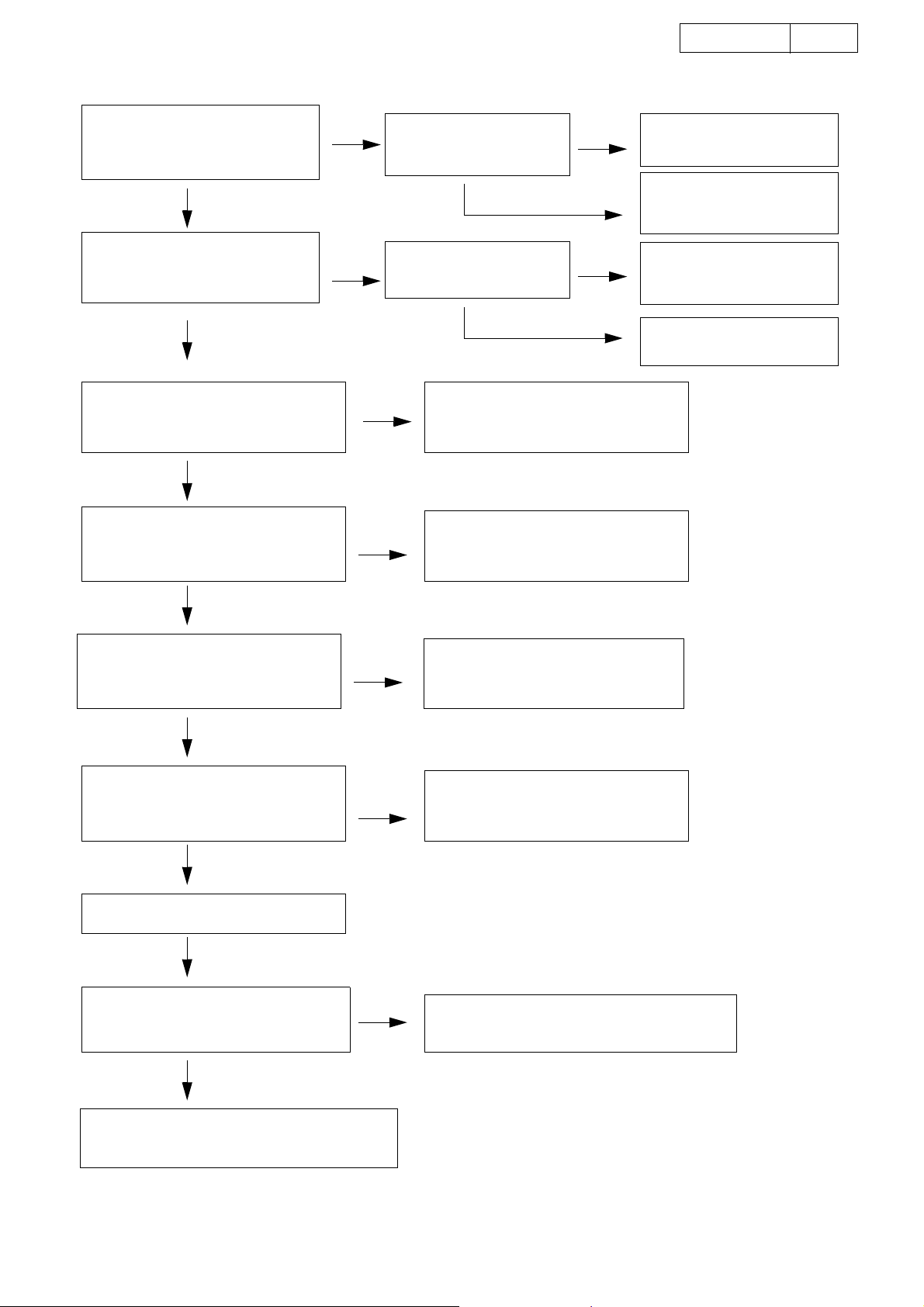
DISASSEMBLY
(Follow the procedure below in reverse order when reassembling.)
After removing the Top Cover, proceed as follows.
1.Loader Panel, Front Panel
1.1. When the Disc Tray can be ejected electrically
(1) Plug the power cord to the wall outlet, switch on the pow-
er, and press the "OPEN/CLOSE" button to open the
Disc Tray.
(2) Detach the Loader Panel by lifting it in the arrow direc-
tion.
(3) Press the "OPEN/CLOSE" button to close the Disc Tray,
then unplug the power cord.
(4) Remove 2 top screws and 4 bottom screws, then detach
the Front Panel to the arrow direction..
Front Panel
Power Switch
各部のはずしかた
(組み立てるときは、逆の順序で行ってください。)
トップカバーをはずした状態で作業します。
1. フロントパネル、ローダーパネルのはずし
かた
1.1.ディスクトレイが電動でオープンできる場合
(1) 電源コードを電源コンセントに差し込み、電源スイッ
チを押し、「OPEN/CLOSE」ボタンを押して、ディスクト
レイをオープンします。
(2) ローダーパネルを矢印の方向に持ち上げ、はずします。
(3)「OPEN/CLOSE」ボタンを押し、ディスクトレイをクロー
ズして、電源コンセントから電源コードを抜きます。
(4) 上からねじ 2 本、下からねじ 4 本をはずし、フロント
パネルを矢印の方向にはずします。
Loader Panel
1.2. When the Disc Tray cannot be ejected
electrically
(1) Insert a straight ruler etc. into the left side of the Mecha.
Unit and push the A-part (see Fig.) to open the Disc
Tray manually.
(2) Detach the Loader Panel by lifting it in the arrow direc-
tion.
(3) Push the Disc Tray to close it manually.
(4) Detach the Front Panel following the same steps de-
scribed on the previous page 1.1.1. (4).
Fig. The left side view of the Mechanism.
"OPEN/CLOSE"button
1.2.ディスクトレイが電動でオープンできない場合
(1) メカユニットの左側から定規等を差し込み、A 部を押し
て、ディスクトレイをオープンします。
(2) ローダーパネルを矢印方向に持ち上げ、はずします。
(3) ディスクトレイを押して、クローズします。
(4) 前項 1.1.1. の(4)と同様に、フロントパネルをはず
します。
A-part
A straight ruler etc.
3
DVD-2200
4
2.DVD Mecha.
(1) Remove 4 screws fixing the Mecha. Cover and detach
the Mecha. Cover.
(2) Remove 4 screws on the DVD Mecha. and 2 screws on
the Main P.W.B., then take it off in the arrow direction.
DVD Mecha.
2. DVD メカのはずしかた
(1) メカカバーの取付けねじを 5 本はずし、メカカバーを
取りはずします。
(2) DVD メカからねじ 4 本、メイン基板からねじ 2 本をはず
し、矢印の方向へ DVD メカをはずします。
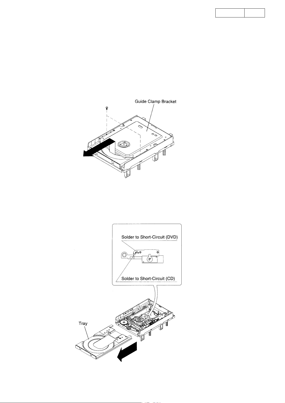
3.Mecha.Unit
(1) Remove 2 screws on the top of the Mecha. Unit, and de-
tach the Guide Clamp Bracket with sliding in the arrow direction.
(2) Solder the short-circuit on the Traverse Unit. (Refer to
"Traverse Unit Disassembly" on page 5.
(3) Disconnect the wires (CX151, CX241, CX031, CX051)
connecting with the Main PWB.
(4) Turn over the Mecha. Unit/Main PWB assembly, and re-
move 3 screws.
3. メカユニットのはずしかた
(1) メカの上からねじ 2 本をはずし、ガイドクランプブラ
ケットを矢印方向にずらしながらはずします。
(2) ドライバーメカのショートサーキットを半田付けしま
す。(トラバースユニットのはずしかた 5 ページ参照)
(3) メイン基板と接続しているワイヤー(CX151, CX241,
CX031, CX051)をはずします。
(4) 一体のメカユニット / メイン基板を裏返し、ねじ 2 本
をはずします。
4
DVD-2200
5
4.Traverse Unit Disassembly
Caution: The optical pickup can be damaged easily
by static electricity charged on human body. Take
necessary anti-static measures when repairing
around the optical pickup.
4.1. Guide Clamp Bracket disassembly
(1) Remove 2 screws.
(2) Remove Guide Clamp Bracket to arrow direction.
4. トラバースユニットのはずしかた
注意:光ピックアップは、人体に帯電した静電気等
で静電破壊することがあります。光ピックアップ周
辺を修理する際は、必要な静電対策を行ってくださ
い。
4.1.ガイドクランプブラケットのはずしかた
(1) ねじ 2 本をはずします。
(2) ガイドクランプブラケットを矢印方向にとりはずしま
す。
4.2. Tray disassembly
(1) Remove to arrow direction.
(2) Solder the short-circuit (see in the frame).
4.2.トレイのはずし方
(1) 矢印方向にとりはずします。
(2) 半田付けショートを行います。(枠内図参照 )
5
DVD-2200
6
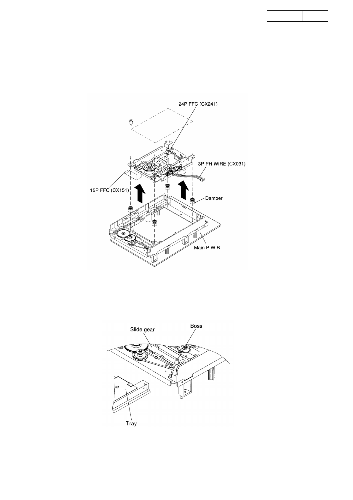
4.3. Traverse Unit disassembly
(1) Remove 24P FFC (CX241), 15P FFC (CX151), 5P PH
WIRE (CX051) and 3P PH WIRE (CX031) connecting
with from the Main P.W.B.
(2) Remove 4 screws fixing Damper.
(3) Remove Traverse Unit to arrow direction.
4.3.トラバースユニットのはずしかた
(1) メイン基板に接続している 24P FFC(CX241)、15P FFC
(CX151),5P PH ワイヤ(CX051)、3P PH ワイヤ(CX031)
をはずします。
(2) ダンパーを固定しているねじ 4 本をはずします。
(3) トラバースユニットを矢印方向にとりはずします。
Note for disassembly Traverse Unit
(1) When assembling, reverse the order of the above.
(2) When inserting Tray, confirm boss on Slide Cam set to
ditch of the Tray (Compare with below drawing).
トラバースユニット分解の注意
(1) 組み立てるときは、上記の逆の順序で行ってください。
(1) トレイ組込み時、スライドカムのボスがトレイの溝に
合っているか確認してください。(下図参照)
6
DVD-2200
7
DIAGNOSTICS OF OPTICAL PICKUP
AND REPLACING TRAVERSE UNIT
Make failure diagnostics of the Optical Pickup as follows.
If the laser drive current becomes more than 1.5 times of the
initial value, the Optical Pickup should be replaced.
The laser drive current is registered on the seal attached to
the rear of the Mecha.Unit.
In case of replacing the Pickup, change the whole part of the
Traverse Unit.
No mechanical adjustment is necessary after the replacement.
Example:
例:
DVD 30mA
CD 30mA
光ピックアップの故障診断とトラバース
ユニットの交換
次の順序で故障診断を行ってください。
レーザー駆動電流が初期値の 1.5 倍以上になっている場合は
光ピックアップ交換の目安となります。
レーザーの電流初期値は、メカの後部のシール上に記入され
ています。
ピックアップ交換の場合は、トラバースユニット単位での交
換となります。メカの調整は不要です。
Disc no read,unsteady playback, etc.
Laser drive current check
HF wave form check
(Refer to WAVE FORMS)
Present value exceeds the initial value by 1.5 times
Traverse Unit replacing
(See page 5 for details)
ディスクを読み込まない
スムーズに再生しない、等
レーザー駆動電流の確認
HF 波形の確認
(
WAVE FORMS
トラバースユニット交換
(詳細は 5 ページ)
参照)
現在値が初期値の
1.5 倍になっている
Laser current registering after replacement.
Step: Disc playback
Write the measured value on the seal attached to the
Mecha. Unit
*As to the measuring method, refer to page 9.
交換後のレーザー電流記入
手順 :ディスクを再生
その時の Iop 値をメカ後方のシールの上に重ねて貼る
等で更新する。
*Iop の測定方法は、9 ページ参照。
7

DVD-2200
Laser current consumption value
ex) DVD
***
mA, CD
***
mA
レーザー駆動電流値
例)
DVD
***
mA, CD
***
mA
8
1. Label Indication of DVD Mechanism.
2. Note for Handling the Laser Pick-Up
the protection for the damage of laser diode.
If you want to change the optical device unit from any other
units, you must keep the following.
(1) It should be done at the desk already took measures the
static electricity in care of removing the OPU's (Optical
device unit) connector cable.
(2) Workers should be put on the "Earth Band".
(3) It should be done to add the solder to the short land to
prevent the broken Laser diode before removing the 24P
FFC cable.
(4) Don't touch OPU's connector parts carelessly.
1.DVD メカのラベル表示
2.レーザーピックアップの取扱注意
レーザーダイオードの破壊防止。
光素子ユニットを交換するときは、以下を遵守してくださ
い。
(1)光素子ユニットの接続ケーブルをはずすときは、静電対
策を行ったデスク上で作業してください。
(2)作業者は、リストストラップを使用してください。
(3)レーザーダイオードの破壊防止のため、24P FFC ケーブ
ルをはずす前にランドを半田付けショートしてくださ
い。
(4)光素子ユニットのコネクタ部に触れないでください。
3. Replacement of the Laser Pick-up
(Traverse Unit)
Check the Iop(Laser drive current)
If the present Iop (current) value exceeds.+50% of the ini-
tial value, replace the Traverse unit(Laser Pick-up) with a
new one.
4. Iop Measurement Method
When measuring Laser drive current (Iop), playback the
discs (CD,DVD) described below, measure Iop for CD
Laser and DVD Laser by the test point (+5V-A2 --LD(CD),
LD(DVD)) on the Main P.W.B.
Test Disc :DVD/DVDT-S01 or commercially available discs.
:CD/TCD-784 (manufactured by ALMEDIO INC)
or commercially available discs.
3.レーザーピックアップ ( トラバースユニッ
ト ) の交換
Iop( レーザー駆動電流)をチェックします。
現在の Iop 値が初期値の 150%を越えている場合、トラ
バースユニット(レーザーピックアップ)を交換してく
ださい。
4.Iop の測定方法
レーザー駆動電流を測定する場合、下記のディスク
(CD,DVD) を再生します。
Main 基板上のテストポイント(+5V-A2 ~ LD(CD),
LD(DVD))にて、CD レーザーと DVD レーザーの Iop を測
定してください。
テストディスク:DVD/DVDT-S01 または市販同等ディスク
:CD/TCD-784(ALMEDIO 社製)または市販
同等ディスク
8
DVD-2200
LD(DVD)
+5V-A2
Oscilloscope
LD(DVD)
LD(CD)
+5V-A2
Main Unit foil side
9
4.1. DVD Laser current measurement
LD(DVD)
+5V-A2
Oscilloscope
(1) Connect the oscilloscope to +5V-A2 of test point for GND
side and LD(DVD) of test point for signal side.
(2) Playback the title 1 / chapter 1 of the DVD Test Disc.
(3) Measure the voltage between +5V-A2 and LD(DVD), cal-
culate Iop by the formula as shown below.
Iop
Measurement Voltage Value
-----------------------------------------------------------------------------=
14 (Resistance value)
4.2. CD Laser current measurement
(1) Connect the oscilloscope to +5V-A2 of test point for GND
side and LD(CD) of test point for signal side.
(2) Playback the track 1 of the CD Test Disc.
(3) Measure the voltage between +5V-A2 and LD(CD), calcu-
late Iop by the formula as shown below.
4.1.DVD レーザー電流測定
(1)オシロスコープをテストポイント +5V-A2(GND) と
LD(DVD)( 信号 ) へ接続します。
(2)DVD テストディスクのタイトル 1・チャプター1 を再生し
ます。
(3)+5V-A2 と LD(DVD) 間の電圧を測定し、次式により Iop を
算出します。
Iop
測定電圧値
--------------------=
14(抵抗値)
4.2.CD レーザー電流測定
(1)オシロスコープをテストポイント +5V-A2(GND) と
LD(CD)( 信号 ) へ接続します。
(2)CD テストディスクのトラック 1 を再生します。
(3)+5V-A2 と LD(CD) 間の電圧を測定し、次式より Iop を算
出します。
Iop
Measurement Voltage Value
-----------------------------------------------------------------------------=
11.75 (Resistance value)
Iop
測定電圧値
--------------------------=
11.75(抵抗値)
9
DVD-2200
10
SERVICE MODE
1. Aging Mode
(1) preparation
(a) Equipment used: Any one of DVD Karaoke Disc (contain-
ing more than 10 titles).
(b) Unit setting : No spec other than the following procedure
(Aging mode).
At the tray open status, press the "POWER" button to
turn on the power while pressing the "PLAY" and
"OPEN/CLOSE" buttons for DVD operation simulta-
neously. mark on the FL lights, and the unit is set
to the heat run mode.
(2) procedure
(a) According the above, set to the aging mode.
(b) Set a DVD Karaoke disc to the tray and press the "PLAY"
button twice. mark on the FL blinks, and aging
operation(after playback title-1 and title-10 of the disc,
the tray open/close is made automatically, then playback
the title-1 again) starts. This aging operation continues
automatically until it is stopped or it stops caused by an
error. In case of some error in DVD, the tray opens and
the following error messages are displayed on the FL.
No Error contents FL display
1 Bad Disc ERROR 02
2 Focus Error ERROR 02
3 Read Error ERROR 02
4 Tracking Error ERROR 04
5Tray Error ERROR 05
6 Navigation Pack Read Error ERROR 06
サービスモードについて
1.エージングモード
(1) 準備
(a)使用機器:DVD カラオケディスク(10 タイトル以上の
物)。
(b)本体設定:下記設定以外規定無。
(エージングモード)
トレイを開けた状態で DVD ユニットの「再生ボタン」+
「開 / 閉ボタン」を同時に押しながら「電源ボタン」を
押してセットの電源を入れると、FL 管の マーク
が点灯し、ヒートランモードに設定される。
(2) 手順
(a)上記手順でエージングモードに設定する。
(b)トレイに DVD カラオケディスクを入れ、「再生ボタン」
を 2 回押して、FL 管の マークが点滅になると、
「ディスクのタイトル 1 とタイトル 10 を再生した後、
トレイを自動で開 / 閉し、再度タイトル 1 の再生を行
う。」エージング動作になります。停止させるか、エ
ラーにて停止するまでこの動作を自動で繰り返します。
DVD 部にエラーが発生した場合は、FL 管に下表のエ
ラーが表示されます。
No. エラー内容 FL 管表示
1 不良ディスク
2 フォーカスエラー
3 リードエラー
4 トラッキングエラー
5 トレイエラー
6 ナビゲーションパックエラー
ERROR 02
ERROR 02
ERROR 02
ERROR 04
ERROR 05
ERROR 06
2. Initial Setting Mode
(1) Preparation
(a) Equipment used: None
(b) Unit setting: No spec other than the following procedure
(2) Procedure
(a) Initialize the DVD player when µcom, peripheral parts of
com, or Main P.W.B. has been replaced in servicing.
µ
(b) Carry out the following to restore factory setting mode. At
the player stop condition, press 3 buttons for DVD oper-
ation("PLAY", "OPEN/CLOSE", and " SKIP") until
"INITIALIZE" appears and disappears in the FL.
("Initialized" appears and disappears on the TV screen.)
(c) All user setting will be lost and its factory setting will be
restored when this initialization is made. Be sure to memorize your setting for restoring again after the initialization.
2.初期設定モード
(1) 準備
(a)使用機器:無
(b)本体設定:下記手順以外規定無。
(2) 手順
(a)サービスにて、マイコンやマイコン周辺部分やメイン
基板を交換した場合は、DVD プレーヤーの初期化を
行ってください。
(b)セットの初期化を下記の手順で行い、工場出荷モード
に設定する。
セットが停止状態にて、DVD 操作部の「再生ボタ
ン」+「開 / 閉ボタン」+「 ( スキップ)ボタン」
の 3 重押しを FL 管に "INITIALIZE" が表示され消え
るまで押します。(TV 画面には”初期化しました”
が表示され消えます。)
(c)初期化を行うとお客様が設定した内容が工場出荷状態
に戻りますので、あらかじめ設定内容を控えておき初
期化後に再設定してください。
10
DVD-2200
11
3.μ-Com Firm Check Mode
(1) Preparation
(a) Equipment used: None
(b) Unit setting: No spec other than the following procedure.
(2) Procedure
(a) Press the "POWER" button to turn on the power while
pressing the "PLAY" and "OPEN/CLOSE" buttons for
DVD operation simultaneously.
(b) FL all light mode.
This mode is for detecting FL defects. Press "STILL/
PAUSE " on the remote control unit once to light
all FL segments.
(c) DVD µcom and main unit µcom firm check mode. This
mode is for displaying the status of each µcom employed.
DVD µcom firm: Press the "MENU" button or ,
•
button.
Each time the "MENU" button or , bu-
•
ton on the remote control unit is pressed, µcom firm is
displayed one after another.
Ex.: [DRV_030307, B/E 6500,PANEL 6499]
Set Serial No.
(lower 5 digits)
1 00001- Ver.030307
2
3
4
Drive µcom B/E µcom Panel µcom
Ver.6499
(Display)
6499
(Display)
030307
Ver.6500
(Display)
6500
3.マイコンファームチェックモード
(1) 準備
(a)使用機器:無
(b)本体設定:下記手順以外規定無。
(2) 手順
(a)DVD 操作部の「再生ボタン」と「開 / 閉ボタン」を
押しながらセットの「電源ボタン」を押し電源を入れ
ます。
(b)FL 管全点灯 / 全消灯モード。
FL 管の故障判別用のモードで、リモコンの「スティ
ル / ポーズ ボタン」を押すと FL 管が全点灯
します。
(c)DVD マイコン及び本体マイコンのファーム確認モー
ド
搭載されている各マイコンのファーム状態を表示しま
す。
DVD マイコンのファーム:リモコンの「メニューボタ
•
ン」または 、 ボタンを押します。
リモコンのメニューボタンまたは 、 ボタン
•
を押すたびにマイコンファームを次々と表示します。
表示例:〔DRV 030307 、 B/E 6500 、 Panel 6499〕
セットのシ
リアル番号
(下5桁)
1 00001 ~
2
3
4
ドライブマイ
コン
Ver.030307
(表示)030307
B/E マイコン パネルマイコン
Ver.6500
(
) 6500
表示
Ver.6499
(
) 6499
表示
11

DVD-2200
12
4. Setting up the test mode
(1) Setting up
In order to set up the test mode, you press STOP button
•
and REV button simultaneously in the heat-run mode.Fundamentaly, you can set up the test mode at the stop state
after disc loading. (Heat-run mode is set up by pressing
PLAY button,holding OPEN/CLOSE button. If it becomes
heat run mode, PLAY indicator and PAUSE indicator will
light up.)
LOADING display
↓
FL display (The display part of 13 digits)
12345678910111213
T
(2) Mode Select
There are two, servo adjustment value display mode and
•
trace mode (error rate display), in the mode.
(a) If the REV button or the FWD button is pushed in the test
mode, it will become servo adjustment value display
mode.
FL display (The display part of 13 digits)
12345678910111213
T3
(b) If the REV button or the FWD button is pushed again, it
will become the trace mode (error rate display).
FL display (The display part of 13 digits)
12345678910111213
T7
(3) Mode decision
The mode will be decided if the PLAY button is pushed in
•
the state where the mode is chosen.
(a) In the case of servo adjustment value display mode, a
focus offset adjustment value is displayed.
FL display (The display part of 13 digits)
12345678910111213
T31nnnnnnnnnn
(n:adjustment value)
(b) In the case of trace mode (error rate display), trace of
the circumference in one layer is chosen.
FL display (The display part of 13 digits)
12345678910111213
T71FFFFFFFFFF
(F: An address and an error rate display F at the time of undecided.)
(4) Change within the mode
If the REV button or the FWD button is pushed in the state
•
where the mode is decided, a change within the mode will
be made.
(a) In the case of servo adjustment value display mode (re-
fer to table 1 servo adjustment value display mode details)
FL display (The display part of 13 digits)
12345678910111213
TXXnnnnnnnnnn
(XX:selection mode [31--62] n:adjustment value)
4.テストモード
(1) テストモードへの投入
テストモードへの投入はヒートランモード時に STOP
•
キーと REV キーを 2 重押しすることで行う。基本的に
ディスクローディング後の停止状態でテストモードに
投入する。( ヒートランモードへの投入は OPEN/CLOSE
キーと PLAY キーを 2 重押しすることで行う。ヒートラ
ンモードになるとPLAYインジケータと PAUSE インジケー
タが点灯する。)
LOADING 表示
↓
FL 管の表示 (13 桁の表示部 )
12345678910111213
T
(2) モードの選択
モードには、サーボ調整値表示モードとトレースモード
•
( エラーレート表示 ) の 2 つがある。
(a)テストモード投入後に REV キー又は FWD キーを押すと、
サーボ調整値表示モードになる。
FL 管の表示 (13 桁の表示部 )
12345678910111213
T3
(b) 再度 REV キー又は FWD キーを押すとトレースモード (
エラーレート表示 ) になる。
FL 管の表示 (13 桁の表示部 )
12345678910111213
T7
(3) モードの確定
モードを選択してある状態で PLAY キーを押すとモード
•
を確定する。
(a)サーボ調整値表示モードの場合は、フォーカスオフ
セット調整値を表示する。
FL 管の表示 (13 桁の表示部 )
12345678910111213
T31nnnnnnnnnn
(n: 調整値 )
(b)トレースモード ( エラーレート表示 ) の場合は、1層
内周のトレースを選択する。
FL 管の表示 (13 桁の表示部 )
12345678910111213
T71FFFFFFFFFF
(F: アドレス及びエラーレートは未確定時、F を表示する。)
(4) モード内での変更
モードを確定してある状態で REV キー又は FWD キーを押
•
すとモード内での変更を行う。
(a)サーボ調整値表示モードの場合( 表1サーボ調整値表
示モード詳細 参照)
FL 管の表示 (13 桁の表示部 )
12345678910111213
TXXnnnnnnnnnn
(XX: 選択モード [31 ~ 62]、n: 調整値 )
12
DVD-2200
13
(b) In the case of trace mode (error rate display) (refer to ta-
ble 2 trace mode details)
FL display (The display part of 13 digits)
12345678910111213
TYYFFFFFFFFFF
(YY: select mode [71--94] ,F: address and an error rate display F at the
time of undecided)
(5) Execution of trace mode (error rate display)
(refer to table 2 trace mode details)
Trace will be performed if the PLAY button is pushed after
•
choosing operation.
FL display (The display part of 13 digits)
12345678910111213
T Y Y mmmmmml l l l
(YY:select mode[71--94],m:address[PBA][HEX],
l:error rate[COUNT/SEC][HEX])
(Note) Renewal of data is carried out for every CD:300 frame and
DVD:85ECC block.
The mode chosen when selection mode was changed into
•
the trace execution and the PLAY button was pushed is
performed from the beginning.When the PLAY button is
pushed without changing selection mode, the mode under
selection is performed from the beginning.(If the PLAY
button is pushed, the address corresponding to the chosen mode will be searched again.)
(b) トレースモード ( エラーレート表示 ) の場合( 表 2
トレースモード詳細 参照)
FL 管の表示 (13 桁の表示部 )
12345678910111213
TYYFFFFFFFFFF
(YY: 選択モード [71 ~ 94]、F: アドレス及びエラーレートは未確
定時、F を表示する。)
(5) トレースモード ( エラーレート表示 ) の実行(
表 2 トレースモード詳細 参照)
•
動作を選択した後、PLAY キーを押すとトレースを実行す
る。
FL 管の表示 (13 桁の表示部 )
12345678910111213
TYYmmmmmmllll
(YY: 選択モード [71 ~ 94]、m: アドレス [PBA][HEX]、
l: エラーレート [COUNT/SEC][HEX])
(注)CD:300フレーム,DVD:85ECCブロック毎にデータ更新する。
•
トレース実行中に選択モードを変更し、PLAY キーを押す
と選択したモードを最初から実行する。選択モードを変
更せずに PLAY キーを押した場合も、選択中のモードを
最初から実行する。
(PLAY キーを押したら、選択しているモードに対応
したアドレスを再度サーチする。)
(6) Other operation
(a) If the STOP button is pushed into servo adjustment val-
ue display mode and trace mode (error rate display), it
will return to the state at the time of a test mode injection.
FL display (The display part of 13 digits)
12345678910111213
T
(b) Push the OPEN/CLOSE button twice and carry out ser-
vo readjustment in OPEN operation ->CLOSE operation.
(It readjusts with test mode.)
OPEN display
↓
CLOSE display
↓
LOADING display
↓
FL display (The display part of 13 digits)
12345678910111213
T
(c) By pressing STOP button and REV button simulta-
neously in the test mode, it returns to heat-run mode.
(6) その他の動作
(a)サーボ調整値表示モード、トレースモード ( エラー
レート表示 ) 中に STOP キーを押すとテストモード投入
時の状態に戻る。
FL 管の表示 (13 桁の表示部 )
12345678910111213
T
(b)OPEN/CLOSE キーを 2 回押して、OPEN 動作→ CLOSE 動作
で、サーボ再調整する。
( テストモードのまま再調整する。)
OPEN 表示
↓
CLOSE 表示
↓
LOADING 表示
↓
FL 管の表示 (13 桁の表示部 )
12345678910111213
T
(c)テストモード中に STOP キーと REV キーの 2 重押し
( 投入時と同じキー ) で、ヒートランモードに戻る。
13
DVD-2200
14
(7) Test mode detailed table
Table 1: servo adjustment value display mode details
XX Contents
31 RFP FE Offset layer 0 PI of CXD1881AR An offset value and
32 RFP TE Bal
Gain
33 RFP TE
Output Gain
34 RFP TE Offset layer 0 TE offset value of CXD1881AR is
35 DSP TE Offset layer 0 TE offset value inside CXD1885Q is
36 Fcs Bias layer 0 The focus bias value inside
37 Fcs AGC layer 0 The inside focus gain (setting 0x2000
38 Trk AGC layer 0 The inside tracking gain (setting
39 Pi Offset layer 0 It is the parameter calculated inside
40 FE Offset layer 0 It is the parameter calculated inside
41 SE Offset layer 0 It is the parameter calculated inside
42 RFP FE Offset layer 1 PI of CXD1881AR An offset value and
Contents
supplementContents explanation
FE An offset value is displayed.
Pi offset is shown in higher rank
1Byte.
FE offset is shown in low rank 1Byte.
layer 0 TE balance gain value of
layer 0 TE output gain value of CXD1881AR
CXD1881AR is displayed.
is displayed.
displayed.
displayed.
CXD1885Q is displayed.
to 1) value of CXD1885Q is displayed.
Therefore, 0x1FF2 and in the case of
0x2012, it is as follows.
0x1FF2(8178) / 0x2000(8192) =
0.998291015625(fold)
0x2012(8210) / 0x2000(8192) =
1.002197265625(fold)
Notes: The inside of ( ) is a decimal
system equivalent.
0x2000 to 1) value of CXD1885Q is
displayed.
Therefore, 0x1FF2 and in the case of
0x2012, it is as follows.
0x1FF2(8178) / 0x2000(8192) =
0.998291015625(fold)
0x2012(8210) / 0x2000(8192) =
1.002197265625(fold)
Notes: The inside of ( ) is a decimal
system equivalent
CXD1885Q.
The value displayed on a set serves
as the number of complement of 2 of
2Bytes(es) doubled 256.
A voltage value is 6.25mV per bit.
CXD1885Q.
The value displayed on a set serves
as the number of complement of 2 of
2Bytes(es) doubled 256.
A voltage value is 6.25mV per bit.
CXD1885Q.
The value displayed on a set serves
as the number of complement of 2 of
2Bytes(es) doubled 256.
A voltage value is 6.25mV per bit.
FE An offset value is displayed.
Pi offset is shown in higher rank
1Byte.
FE offset is shown in low rank 1Byte.
(7) テストモード詳細一覧表
表 1 サーボ調整値表示モード詳細
XX 内容 内容補足 内容説明
31 RFP FE Offset レイヤ 0 CXD1881AR の PI オフセット値と FE オ
32 RFP TE Bal
Gain
33 RFP TE Output
Gain
34 RFP TE Offset レイヤ 0 CXD1881AR の TE オフセット値を表示。
35 DSP TE Offset レイヤ 0 CXD1885Q 内部の TE オフセット値を表
36 Fcs Bias レイヤ 0 CXD1885Q 内部のフォーカスバイアス
37 Fcs AGC レイヤ 0 CXD1885Q 内部フォ ー カ ス ゲ イ ン
38 Trk AGC レイヤ 0 CXD1885Q 内部トラッキングゲイン (0
39 Pi Offset レイヤ 0 CXD1885Q 内部で計算されるパラメー
40 FE Offset レイヤ 0 CXD1885Q 内部で計算されるパラメー
41 SE Offset レイヤ 0 CXD1885Q 内部で計算されるパラメー
42 RFP FE Offset レイヤ 1 CXD1881AR の PI オフセット値と FE オ
レイヤ 0 CXD1881AR の TE バランスゲイン値を
レイヤ 0 CXD1881AR の TE 出力ゲイン値を表示
フセット値を表示。
上位 1Byte に Pi オフセットを示す。
下位 1Byte に FE オフセットを示す。
表示す。
す。
示。
値を表示。
(0x2000 を 1 として ) 値を表示。
0x1FF2 や 0x2012 の場合、以下のよう
になる。
0x1FF2(8178) / 0x2000(8192) =
0.998291015625( 倍 )
0x2012(8210) / 0x2000(8192) =
1.002197265625( 倍 )
注 :( ) 内は 10 進換算値
x2000 を 1 として ) 値を表示。
0x1FF2 や 0x2012 の場合、以下のよ
うになる。
0x1FF2(8178) / 0x2000(8192) =
0.998291015625( 倍 )
0x2012(8210) / 0x2000(8192) =
1.002197265625( 倍 )
注 :( ) 内は 10 進換算値
タ。
セットに表示される値は、256 倍され
た 2Bytes の 2 の補数となる。
電圧値は 1bit あたり 6.25mV。
タ。
セットに表示される値は、256 倍され
た 2Bytes の 2 の補数となる。
電圧値は 1bit あたり 6.25mV。
タ。
セットに表示される値は、256 倍され
た 2Bytes の 2 の補数となる。
電圧値は 1bit あたり 6.25mV。
フセット値を表示。
上位 1Byte に Pi オフセットを示す。
下位 1Byte に FE オフセットを示す。
43 RFP TE Bal
Gain
44 RFP TE
Output Gain
45 RFP TE Offset layer 1 TE offset value of CXD1881AR is
46 DSP TE Offset layer 1 It is the parameter calculated inside
47 Fcs Bias layer 1 It is the parameter calculated inside
48 Fcs AGC layer 1 The inside focus gain (setting 0x2000
layer 1 TE balance gain value of
layer 1 TE output gain value of CXD1881AR
CXD1881AR is displayed.
is displayed.
displayed.
CXD1885Q.
The value displayed on a set serves
as the number of complement of 2 of
2Bytes(es) doubled 256.
A voltage value is 6.25mV per bit.
CXD1885Q.
The value displayed on a set serves
as the number of complement of 2 of
2Bytes(es) doubled 256.
A voltage value is 6.25mV per bit.
to 1) value of CXD1885Q is displayed.
Therefore, 0x1FF2 and in the case of
0x2012, it is as follows.
0x1FF2(8178) / 0x2000(8192) =
0.998291015625(fold)
0x2012(8210) / 0x2000(8192) =
1.002197265625(fold)
Notes: The inside of ( ) is a decimal
system equivalent.
43 RFP TE Bal
Gain
44 RFP TE Output
Gain
45 RFP TE Offset レイヤ 1 CXD1881AR の TE オフセット値を表示。
46 DSP TE Offset レイヤ 1 CXD1885Q 内部で計算されるパラメー
47 Fcs Bias レイヤ 1 CXD1885Q 内部で計算されるパラメー
48 Fcs AGC レイヤ 1 CXD1885Q 内部フォ ー カ ス ゲ イ ン
レイヤ 1 CXD1881AR の TE バランスゲイン値を
レイヤ 1 CXD1881AR の TE 出力ゲイン値を表示。
表示。
タ。
セットに表示される値は、256 倍され
た 2Bytes の 2 の補数となる。
電圧値は 1bit あたり 6.25mV。
タ。
セットに表示される値は、256 倍され
た 2Bytes の 2 の補数となる。
電圧値は 1bit あたり 6.25mV。
(0x2000 を 1 として ) 値を表示。
0x1FF2 や 0x2012 の場合、以下のよう
になる。
0x1FF2(8178) / 0x2000(8192) =
0.998291015625( 倍 )
0x2012(8210) / 0x2000(8192) =
1.002197265625( 倍 )
注 :( ) 内は 10 進換算値
14
DVD-2200
15
49 Trk AGC layer 1 The inside tracking gain (setting
50 Pi Offset layer 1 It is the parameter calculated inside
51 FE Offset layer 1 It is the parameter calculated inside
52 SE Offset layer 1 It is the parameter calculated inside
53 PO error
detection number
54 PO uncorrect-
able error
number
55 PI error detec-
tion number
56 PI uncorrect-
able error
number
57 Mirr Count Disc dis-
58 Mirr Width Disc dis-
59 FZC Count Disc dis-
60 Pi Level Disc dis-
61 Disc Type Disc Type They are the contents at the time of
62 PO error
detection
number and
address
Error rate It is invalid at the time of CD
Error Rate It is invalid at the time of CD
Error Rate CD : C1 error detection number
Error Rate CD : C2 uncorrectable error number
criminant
criminant
criminant
criminant
Error rate PO error detection number is invalid
0x2000 to 1) value of CXD1885Q is
displayed.
Therefore, 0x1FF2 and in the case of
0x2012, it is as follows.
0x1FF2(8178) / 0x2000(8192) =
0.998291015625(fold)
0x2012(8210) / 0x2000(8192) =
1.002197265625(fold)
Notes: The inside of ( ) is a decimal
system equivalent
CXD1885Q.
The value displayed on a set serves
as the number of complement of 2 of
2Bytes(es) doubled 256.
A voltage value is 6.25mV per bit.
CXD1885Q.
The value displayed on a set serves
as the number of complement of 2 of
2Bytes(es) doubled 256.
A voltage value is 6.25mV per bit.
CXD1885Q.
The value displayed on a set serves
as the number of complement of 2 of
2Bytes(es) doubled 256.
A voltage value is 6.25mV per bit.
operation.
operation.
They are the contents at the time of
disc distinction.
Please refer to "Table 3 Disc
distinction information" about the
contents of a value.
They are the contents at the time of
disc distinction.
Please refer to "Table 3 Disc
distinction information" about the
contents of a value.
They are the contents at the time of
disc distinction.
Please refer to "Table 3 Disc
distinction information" about the
contents of a value.
They are the contents at the time of
disc distinction.
Please refer to "Table 3 Disc
distinction information" about the
contents of a value.
disc type.
Please refer to "Table 4 Disc
classification information" about the
contents of a value.
at the time of CD operation.
49 Trk AGC レイヤ 1 CXD1885Q 内部 ト ラ ッ キ ン グ ゲ イ ン
50 Pi Offset レイヤ 1 CXD1885Q 内部で計算されるパラメー
51 FE Offset レイヤ 1 CXD1885Q 内部で計算されるパラメー
52 SE Offset レイヤ 1 CXD1885Q 内部で計算されるパラメー
53 PO 誤り検出数 エ ラ ー
54 PO 訂正不可数 エ ラ ー
55 PI 誤り検出数 エ ラ ー
56 PI 訂正不可数 エ ラ ー
57 Mirr Count デ ィ ス ク判別ディスク判別時の内容。
58 Mirr Width デ ィ ス ク判別ディスク判別時の内容。
59 FZC Count デ ィ ス ク判別ディスク判別時の内容。
60 Pi Level デ ィ ス ク判別ディスク判別時の内容。
61 Disc Type デ ィ ス ク種別ディスク種別の内容。
62 PO 誤り検出数
とアドレス
レート
レート
レート
レート
エラー
レート
(0x2000 を 1 として ) 値を表示。
0x1FF2 や 0x2012 の場合、以下のよ
うになる。
0x1FF2(8178) / 0x2000(8192) =
0.998291015625( 倍 )
0x2012(8210) / 0x2000(8192) =
1.002197265625( 倍 )
注 :( ) 内は 10 進換算値
タ。
セットに表示される値は、256 倍され
た 2Bytes の 2 の補数となる。
電圧値は 1bit あたり 6.25mV。
タ。
セットに表示される値は、256 倍され
た 2Bytes の 2 の補数となる。
電圧値は 1bit あたり 6.25mV。
タ。
セットに表示される値は、256 倍され
た 2Bytes の 2 の補数となる。
電圧値は 1bit あたり 6.25mV。
CD 時は無効。
CD 時は無効。
CD 時は C1 誤り検出数。
CD 時は C2 訂正不可数。
値の内容は「表3ディスク判別情報」
を参照。
値の内容は「表3ディスク判別情報」
参照。
値の内容は「表3ディスク判別情報」
参照。
値の内容は「表3ディスク判別情報」
参照。
値の内容は「表4ディスク種別情報」
参照。
CD 時は PO 誤り検出数は無効。
15
DVD-2200
16
Table 2: trace mode details
YY Contents Contents supplement
71 A display of PO error detection
number of the inner circumference of 1-layer and an address.
72 A display of PO uncorrectable
number of the inner circumference of 1-layer and an address.
73 A display of PI error detection
number of the inner circumference of 1-layer and an address.
74 A display of PI uncorrectable
number of the inner circumference of 1-layer and an address.
75 A display of PO error detection
number of the central circumference of 1-layer and an address.
76 A display of PO uncorrectable
number of the central circumference of 1-layer and an address.
77 A display of PI error detection
number of the central circumference of 1-layer and an address.
78 A display of PI uncorrectable
number of the central circumference of 1-layer and an address.
79 A display of PO error detection
number of the outer circumference of 1-layer and an address.
80 A display of PO uncorrectable
number of the outer circumference of 1-layer and an address.
81 A display of PI error detection
number of the outer circumference of 1-layer and an address.
82 A display of PI uncorrectable
number of the outer circumference of 1-layer and an address.
83 A display of PO error detection
number of the inner circumference of 2-layer and an address.
84 A display of PO uncorrectable
number of the inner circumference of 2-layer and an address.
85 A display of PI error detection
number of the inner circumference of 2-layer and an address.
86 A display of PI uncorrectable
number of the inner circumference of 2-layer and an address.
87 A display of PO error detection
number of the central circumference of 2-layer and an address.
88 A display of PO uncorrectable
number of the central circumference of 2-layer and an address.
89 A display of PI error detection
number of the central circumference of 2-layer and an address.
90 A display of PI uncorrectable
number of the central circumference of 2-layer and an address.
91 A display of PO error detection
number of the outer circumference of 2-layer and an address.
92 A display of PO uncorrectable
number of the outer circumference of 2-layer and an address.
93 A display of PI error detection
number of the outer circumference of 2-layer and an address.
94 A display of PI uncorrectable
number of the outer circumference of 2-layer and an address.
It is invalid at the time of CD
operation.
It is invalid at the time of CD
operation.
CD : C1 error detection number
CD : C2 uncorrectable error
number
It is invalid at the time of CD
operation.
It is invalid at the time of CD
operation.
CD : C1 error detection number
CD : C2 uncorrectable error
number
It is invalid at the time of CD
operation.
It is invalid at the time of CD
operation.
CD : C1 error detection number
CD : C2 uncorrectable error
number
In the case of 1-layer disc, it is
invalid.
In the case of 1-layer disc, it is
invalid.
In the case of 1-layer disc, it is
invalid.
In the case of 1-layer disc, it is
invalid.
In the case of 1-layer disc, it is
invalid.
In the case of 1-layer disc, it is
invalid.
In the case of 1-layer disc, it is
invalid.
In the case of 1-layer disc, it is
invalid.
In the case of 1-layer disc, it is
invalid.
In the case of 1-layer disc, it is
invalid.
In the case of 1-layer disc, it is
invalid.
In the case of 1-layer disc, it is
invalid.
表 2 トレースモード詳細
YY 内容 補足説明
71 1 層内周の PO 誤り検出数とアド
レスの表示
72 1 層内周の PO 訂正不可数とアド
レスの表示
73 1 層内周の PI 誤り検出数とアド
レスの表示
74 1 層内周の PI 訂正不可数とアド
レスの表示
75 1 層中周の PO 誤り検出数とアド
レスの表示
76 1 層中周の PO 訂正不可数とアド
レスの表示
77 1 層中周の PI 誤り検出数とアド
レスの表示
78 1 層中周の PI 訂正不可数とアド
レスの表示
79 1 層外周の PO 誤り検出数とアド
レスの表示
80 1 層外周の PO 訂正不可数とアド
レスの表示
81 1 層外周の PI 誤り検出数とアド
レスの表示
82 1 層外周の PI 訂正不可数とアド
レスの表示
83 2 層内周の PO 誤り検出数とアド
レスの表示
84 2 層内周の PO 訂正不可数とアド
レスの表示
85 2 層内周の PI 誤り検出数とアド
レスの表示
86 2 層内周の PI 訂正不可数とアド
レスの表示
87 2 層中周の PO 誤り検出数とアド
レスの表示
88 2 層中周の PO 訂正不可数とアド
レスの表示
89 2 層中周の PI 誤り検出数とアド
レスの表示
90 2 層中周の PI 訂正不可数とアド
レスの表示
91 2 層外周の PO 誤り検出数とアド
レスの表示
92 2 層外周の PO 訂正不可数とアド
レスの表示
93 2 層外周の PI 誤り検出数とアド
レスの表示
94 2 層外周の PI 訂正不可数とアド
レスの表示
CD 時は無効。
CD 時は無効。
CD 時は C1 誤り検出数。
CD 時は C2 訂正不可数。
CD 時は無効。
CD 時は無効。
CD 時は C1 誤り検出数。
CD 時は C2 訂正不可数。
CD 時は無効。
CD 時は無効。
CD 時は C1 誤り検出数。
CD 時は C2 訂正不可数。
1 層ディスクの場合、無効。
1 層ディスクの場合、無効。
1 層ディスクの場合、無効。
1 層ディスクの場合、無効。
1 層ディスクの場合、無効。
1 層ディスクの場合、無効。
1 層ディスクの場合、無効。
1 層ディスクの場合、無効。
1 層ディスクの場合、無効。
1 層ディスクの場合、無効。
1 層ディスクの場合、無効。
1 層ディスクの場合、無効。
16
DVD-2200
17
Table 3:Disc distinction information
Mirr Coun
No Disc Except 2
CD High reflection
CD Low reflection
DVD High
reflection
DVDLow reflection
DVD 2-layer 2 Less than
SACD Hybrid 3 - - -
tMirr Width
and 3
2 More than
2 More than
2 Less than
2 Less than
0x8ED
0x8ED
0x8E9
0x8E9
0x8E9
FZC Coun
---
tPI Level
- More than
- Less than
1 More than
1 Less than
2-
0x99
0x98
0x81
0x80
PI level Formula : PI level (V) = Measured value x 1.6÷256
"-" : Invalid
Table 4: Disc classification information
Disc Type Media
0x00 No Disc
0x01 Unknown Disc
0x04 DVD Single High reflection
0x05 DVD Dual Parallel Low reflection
0x06 DVD Dual Opposite Low reflection
0x08 CDDA High reflection
0x0A VCD High reflection
0x44 DVD Single Low reflection
0x48 CDDA Low reflection
0x4A VCD Low reflection
0x8F SACD Hybrid Disc
表3 ディスク判別情報
Mirr Coun
No Disc 2 と 3 以外 - - CD 高反射 2 0x8ED 以上 - 0x99 以上
CD 低反射 2 0x8ED 以上 - 0x98 以下
DVD 高反射 2 0x8E9 以下 1 0x81 以上
DVD 低反射 2 0x8E9 以下 1 0x80 以下
DVD 2 層 2 0x8E9 以下 2 SACD Hybrid 3 - - -
t Mirr Width
FZC Coun
t PI Level
PI level 計算式:PI level (V) = 測定値× 1.6 ÷ 256
"-" は無効
表4 ディスク種別情報
Disc Type Media
0x00 No Disc
0x01 Unknown Disc
0x04 DVD Single 高反射
0x05 DVD Dual Parallel 低反射
0x06 DVD Dual Opposite 低反射
0x08 CDDA 高反射
0x0A VCD 高反射
0x44 DVD Single 低反射
0x48 CDDA 低反射
0x4A VCD 低反射
0x8F SACD Hybrid Disc
17
TROUBLE SHOOTING
1. GU-3570 MAIN PWB
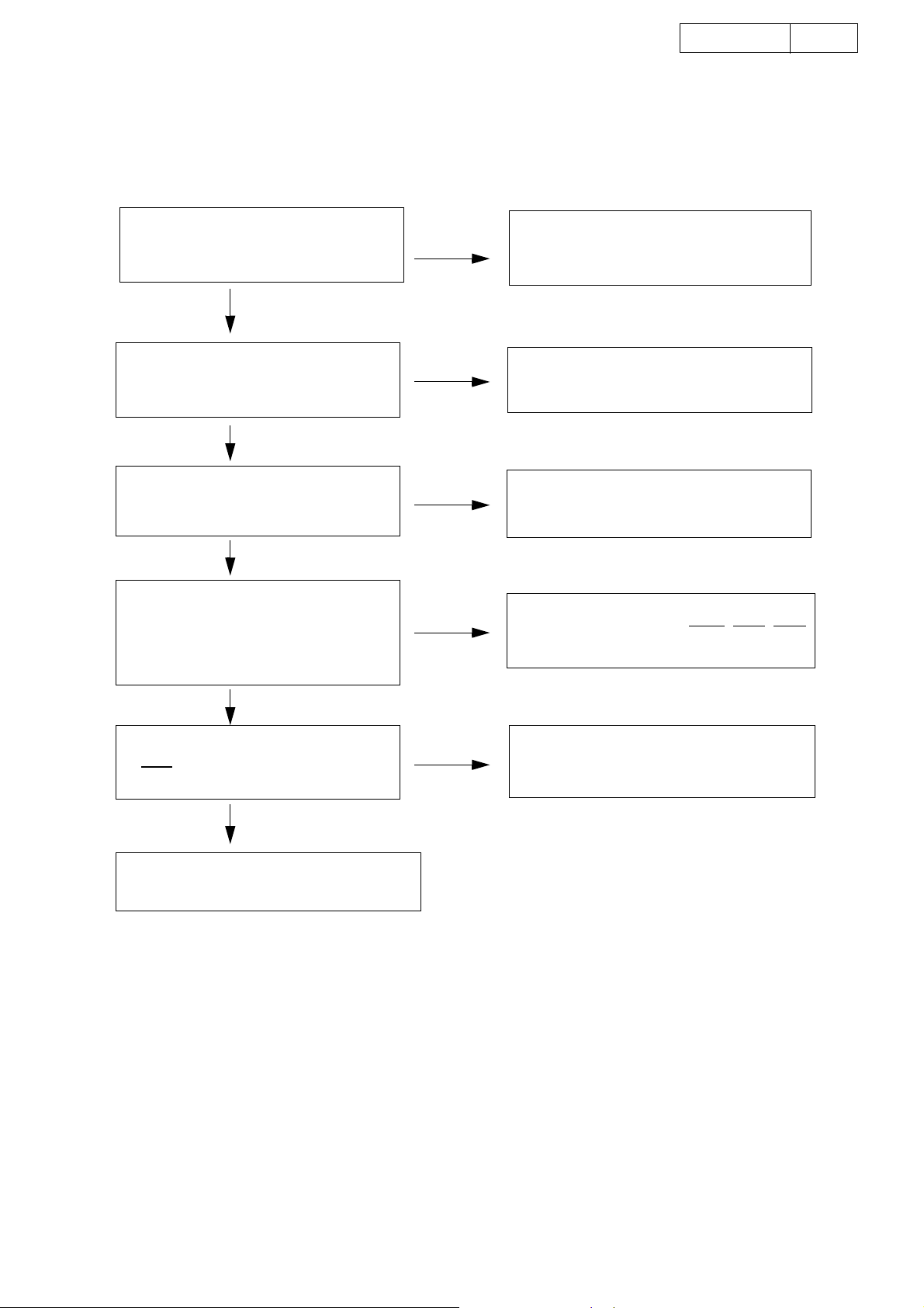
1.1. FL TUBE doesnít light
(1) Check the Set-up process of Panel µ-COM
Check Power Supply Voltages.
•
[IC301]:D1,D4
+3.3V_D1, +3.3V_D4
O.K.
N.G.
Check soldering.
•
CY121 on MAIN PWB.
DVD-2200
18
Check Oscillation Waveform.
•
[IC301]:
25MHz at 31pin.
O.K.
Check Reset Signal.
•
[IC301]:
"H" level at 35pin?
O.K.
Check Data Bus between
IC301 and IC302(Flash ROM):
•
Does the level change at FD(0--15)
Pins of IC301
O.K.
Check Data Bus between
FLD Driver(GU-3571-3 [IC101])
•
[RST]:
"H" level?
N.G.
N.G.
N.G.
N.G.
Check soldering.
•
X301 on MAIN PWB.
Check soldering.
•
IC303(Reset IC) on MAIN PWB.
Check soldering.(short-circuit,open)
•
FD(0--15), PA(1--16), PWE, PCE, POE,
(1)Check soldering of CX171.
(2)GU-3571-3 is N.G.(No Good).
O.K.
Continue to next step.
Check the Set-up process of B/E µ-COM.
18
(2) Check the Set-up process of B/E µ-COM.
DVD-2200
19
Check Power Supply Voltages.
•
[IC102]:
+3.3V_D1, +2.5V_D1 O.K.?
O.K.
Check Clock waveform.
•
[IC102]:18 pin.
27MHz (3.3V), O.K.?
O.K.
Check Reset signal.
•
[IC102]:(MC-TRST) 15 pin.
"H" level O.K.?
O.K.
Check Power Supply Voltages.
•
[IC101]:
+3.3V_D1, +1.8V_D1 O.K.?
N.G.
N.G.
Check the output level.
[ON/ST]: "H" level?
Check 27MHz(3.3V) at
4pin of IC105.
N.G.
N.G.
Check soldering
•
[IC301]: 37pin.
•
R310 and R311.
Check soldering
•
[IC117] and [IC118]
•
[FB101] and [FB102].
N.G.
O.K.
N.G.
O.K.
Check soldering.
•
[IC301]: 55pin.
Check the circumference
soldering.
•
[FB108, FB109]
(1)Check soldering of X101.
(2)Check soldering of IC105
(SM8707).
Check soldering of R168
and R153.
O.K.
Check Clock waveform.
•
[IC101]:106 pin.
27MHz (3.3V), O.K.?
O.K.
Check Clock waveform.
•
[IC101]:172 pin.
24.576MHz (3.3V), O.K.?
O.K.
[IC101] Reset Check.
O.K.
Check Address, Data Bus between
[IC102] and [IC103](Flash Rom).
N.G.
N.G.
N.G.
Check soldering
•
[IC105]: 3pin.
•
R170, R101.
Check soldering
•
[IC105]: 9pin.
•
R174, R133.
Check soldering at Address, Data Bus.
•
[MCD0--MCD14], [MCA11--MCA30]
O.K.
Continue to next step.
Check the Set-up process of F/E µ-COM.
19
(3) Check the Set-up process of F/E µ-COM.
DVD-2200
20
Check Power Supply Voltages.
•
[IC502]:
+3.3V_D2, +1.8V_D2 O.K.?
+3.3V_A2, +1.8V_A2 O.K.?
O.K.
Check Clock waveform.
•
[IC502]:33 pin.
33.87MHz (3.3V), O.K.?
O.K.
Check Reset signal.
•
[IC502]:(DRVRST) 51 pin.
"H" level O.K.?
O.K.
END
N.G.
N.G.
N.G.
Check soldering
•
[IC114], [IC115]
•
FB405 and FB408.
Check soldering
•
[IC105]: 15pin.
•
R171.
•
[IC405], R697 and R574
Check soldering
•
[IC102]: 108pin.
•
R129, R635 and R570.
1.2. Image is not displayed. (Blue-back, DENON wallpaper)
Check Digital output signal for Video.
•
[IC101]: PXD(0--7), VCLK
N.G.
Check soldering
•
[IC101]: 183--192pin.
•
RA101, RA102, R125 and R126.
O.K.
Check Digital input signal for Video.
•
[GU-3572]: YUV(0--7), VCLK
N.G.
Check soldering
•
[CX331]
O.K.
Continues to the Check process of GU-3572 VIDEO P.W.B..
20
1.3. Does not Read Disc
[No PLAY], [00 00] displayed etc.
(1) Disc does not Rotate.
DVD-2200
21
Check the Emission of Pick-up.
•
Emission of PU laser O.K.?
* See attached sheet
laser
current check
(Page 8,9)
O.K.
Check Spindle drive signal.
•
[DMO]: "H" level?
O.K.
END
(2) CD check process
Check the RF signal.
Check the voltage of Test-Point(TP)
•
TP [RFAC]: about 1V
p-p.
N.G.
N.G.
N.G.
(1)Check soldering of P.U.
•
short-circuit?
(2)Check the circumference soldering of TR501
and TR502.
(3)Check connector insertion
•
[P.U.] -- [GU3570] FFC(CX241)
(4)Check soldering.
•
[IC501], CXD1881AR
(5)Check soldering.
•
[IC508]: FAN8042
Check soldering
•
[IC502]: 111--113pin check.
•
R599, R601, R666--R669
•
[IC505]
Check soldering
•
[IC501]: circumference soldering check.
•
[IC502]: 65--110pin check.
O.K.
Check Connection.
•
[IC502]--[IC503](16MDRAM)
"L"--"H" alternate?
O.K.
END
(3) DVD check process
Check VSTEM. (communication)
•
VDT(0--7)_COR,
•
XHAC_COR, VEFG_COR,
•
XSHD_COR, DCK_COR
"L"--"H" alternate?
O.K.
Check Request Signal
•
Request From [B/E] to [F/E]
[HDRQ_COR]:
"L"
level?
N.G.
N.G.
N.G.
Check soldering
•
[BD(0-15)], [BA(0-9)], [XLCOS], [XUCAS]
[XMOE], [XRAS], [XMWR].
•
[IC502], [IC503]
Check soldering
•
[IC502]: 36--49pin
•
R621--R633
•
R401--411.
Check soldering
•
[IC404]
END
O.K.
21
(4) SACD check process
Check communication.
•
[VSTEM]: communication
"L"--"H" level alternate?
O.K.
N.G.
Check soldering
•
[IC404]
•
R437--R449.
DVD-2200
22
Check RF signal for Water Mark.
•
TP [WM]: about 1V
p-p.
O.K.
Check Bus Line.
Between IC401 and IC402(16MSDRAM)
"L"-"H" level alternate?
O.K.
END
N.G.
N.G.
Check soldering
•
[IC403]: Circumference soldering check
Check soldering
•
[IC401]: 141--162pin.
•
[IC402]
22
1.4. No sound, Noise generated
(1) CD
DVD-2200
23
Check CD digital Audio data output.
•
[CDLRCK], [CDBCLK], [CDDIN], [DOTX]
N.G.
Check soldering
O.K.
Check digital Audio data output.
•
[IC101]: [DATA1], [LRCK], [BCK],
N.G.
Check soldering
[DOUT0]
O.K.
Check Audio select output.
•
[DAD0],[DAWS], [DABCK], [MCLK]
N.G.
Check soldering
O.K.
Continues to the Check process of GU-3571-1 AUDIO P.W.B..
•
[IC502]: 58--62pin check.
•
R641--R644
•
[IC101]: 159--170pin check.
•
R134--R142
•
[IC204]--[IC207]
•
[CX271]
•
[IC106] [IC107]
(2) SACD
Check DSD data output.
•
[IC401]: [DSARS], [DSALS], [DSASW],
[DSAC], [DSAR], [DSAL], [BCKAO]
N.G.
Check soldering
•
[IC401]: 60--76pin check.
•
R450--R456
O.K.
Check audio select output.
•
[DAD1], [DAD2], [DAD0], [DAWS],
[DABCK], [MCLK]
N.G.
(1) Check soldering
•
[IC204]-- [IC207]
•
CX271
(2) Check [IC204, 205]
•
O.K.
DSD/PCM ① Pin
Continues to the Check process of GU-3571-1 AUDIO P.W.B..
"H"
23

(3) DVD-VIDEO / AUDIO
DVD-2200
24
Check DVD digital data output.
•
[IC101]: [DATA(1--3)], [LRCK], [BCK]
O.K.
Check Bus-manager output.
•
[IC201]: [MELD(0--2)], [MELWS],
[MELBCK]
O.K.
Check audio select output.
[DAD0-2)], [DAWS], [DABCK], [MCLK]
O.K.
N.G.
N.G.
N.G.
Check soldering
•
[IC101]: 159--170pin check.
•
[IC201]: 46--71pin check.
(1)Check power supply voltage.
•
[IC201]: +3.3V_D1, +2.5V_D1
(2)Check clock oscillation.
•
[IC201]: (X103) 12.288MHz O.K.?
(3)Check control signal
•
[IC201]: [DSPRST], [HDIN], [HDOUT], [HCLK],
[INTRPT], [HCS] O.K.?
(4)Check communication.
•
[IC201]--[IC202](P-ROM)
(5)Check soldering.
•
[IC203]
Check soldering
•
[IC204]--[IC207]
•
[CX271]
Continues to the Check process of GU-3571-1 AUDIO P.W.B..
2. GU-3571-1 AUDIO P.W.B.
2.1. No sound or Noise generated at audio output terminal.
(1) Check Audio Output terminal, then Input pin of ICs.
•
FL, FR IC301 Audio input check See attached sheet waveform (WAVEFORMS ①~④)
•
CNT,SW IC302 Audio input check
•
SL, SR IC303 Audio input check
(2) Check MUTE Circuit and Transistors.
•
Check MUTE circuit Check Transistors
(TR309--TR326)
2.2. Does not output Digital output signal(DOUT).
Check belows
[IC201], [IC202]
[T201], [JK201]
24
3. GU-3572 VIDEO PWB
(1) Progressive output does not outputed.
DVD-2200
25
Check Power Supply Voltages.
+3.3V_D3, +5V_D1, ±5V_V1
+3.3V_V2, +2.5V_V1, +1.8V_D3
O.K.
Check Oscillation circuit.
•
[IC-703]: (MC504) Set-up
20MHz Oscillation.
RESET "H"?
O.K.
Check IC701.
RESET "H"?
O.K.
Check IC704.
RESET "H"?
O.K.
N.G.
N.G.
N.G.
N.G.
Check soldering.
•
[CY331]
•
[IC712] -- [IC714]
Check soldering.
•
[X701]
Check soldering.
•
[IC701]
Check soldering.
•
[IC704]
Check IC601.
RESET "H"?
O.K.
(2) Interlace output does not outputed.
Check IC704.
RESET "H"?
N.G.
N.G.
Check soldering.
•
[IC601]
Check soldering.
•
[IC704]
25

DVD-2200
26
ELECTRICAL ADJUSTMENT FOR VIDEO
ビデオ回路の調整
1. SETTING
(1) Connect the monitor TV to the video output terminal.
(2) Connect the oscilloscope to the Y-signal and C-signal of
S-VIDEO output terminal and each terminate at 75 Ohms.
(3) Connect the oscilloscope to the Y-signal, P
PR-signal of Component video output terminal and each
terminate at 75 Ohms.
Use the 75 Ohms resistance must be 1%
※
(4) DVD test disc : DVDT-S01
BEFORE ADJUSTMENT
2.
2.1. Setting the Oscilloscope as below.
(1) PB/P
(a) TIME/DIV : 2μS
(b) VOLT/DIV : 100mV
(2) Y/C
(a) TIME/DIV : 2μS
(b) VOLT/DIV : 50mV
Power on. Power Supply
USA & Canada : 120V
Europe : 230V
Japan : 100V
R
(Use the probe : x10 )
(Use the probe : x10 )
-signal and
B
1. セッティング手順
(1) セットの VIDEO OUT 端子にテレビモニターを接続する。
(2) セットの S2 VIDEO OUT 端子から Y 信号と C 信号をそれ
ぞれオシロスコープ(終端抵抗:75Ω)に接続する。
(3) セットの COMPONENT VIDEO OUT の各端子(Y/P
れぞれオシロスコープ(終端抵抗:75Ω)に接続する。
※ 75Ω 抵抗は 1%品を使用する事。
(4) DVD テストディスク:DVDT-S01 を用意する。
B/PR
)をそ
2. 調整のまえに
2.1.オシロスコープを下記に設定する。
(1) PB/
(2) Y/C
P
R
(a)TIME/DIV : 2μS
(b)VOLT/DIV : 100mV
(プローブ x10 使用)
(a)TIME/DIV : 2μS
(b)VOLT/DIV : 50mV
(プローブ x10 使用)
電源電圧 :100V
2.2. Preparation
(1) power on.
(2) Push [OPEN/CLOSE] button, then open the Disc Tray.
Set DVD test disc (DVDT-S01) on the Disc Tray, and
then push [CLOSE] button.
(3) FL display appear "STOP", push [PLAY] button to play-
back DVD.
(4) Set the Video output to INTERLACED by remote control
unit.
(Push the [SETUP] button, set to the mode of
VIDEO SETUP.)
(5) Push the [DISPLAY] button of remote control unit and
then appear the ON-Screen Display (GUI) on the monitor
TV.
(6) Push the [12] button, select title 12 of DVD.
(7) Push the [ENTER] button, playback title 12. (color bar
75%)
2.2.準備手順
(1) セットの AC コードをコンセントへ挿入し、セットの電
源を ON する。
(2) セットの「OPEN/CLOSE」ボタンを押しトレイを開き、ト
レイ上に DVD テストディスク(DVDT-S1)をセット後、
「CLOSE] ボタンを押す。
(3) セット表示管上に "STOP" が表示されてから、PLAY ボタ
ンを押し、ディスクを再生する。
(4) リモコンで VIDEO 出力をインターレースモードに設定す
る。
(5) リモコンの DISPLAY ボタンを押しグラフィカル・ユー
ザー・インターフェイス (GUI) 画面を出す。
(6) 番号ボタンの「12」ボタンを押し、Title 12 を選択す
る。
(7) 「ENTER」ボタンを押し、Title 12 を再生する(75%カ
ラーバー信号)。
26
DVD-2200
27
2.3. Procedure
(1) Adjust the signal of S-VIDEO out by the wave of oscillo-
scope.
(a) Target, Y-signal
Point : VR704
Adjustment Value : 1000±20mV
Waveform
Y
Y-signal of S-VIDEO out
(b) Target, C-signal
Point : VR705
Adjustment Value : 286±5mV
Waveform
C
2.3.手順
(1) セットの S2 VIDEO OUT の信号レベルをオシロスコープ
上の波高値で調整する。
(a)Y 信号レベル
調整個所 :VR704
調整値 : 1000 ± 20mV
波形
Y
S2 VIDEO OUT の Y 信号レベル
(b)C 信号レベル
調整個所 :VR705
調整値 : 286 ± 5mV
波形
C
C-signal of S-VIDEO out
(2) Set the Video output to PROGRESSIVE by remote con-
trol unit. (Push the [SETUP] button, set to the mode of
VIDEO SETUP.)
(a) Target, Y-signal
Point : VR701
Adjustment Value : 1000 ±20mV
Waveform
Y
Y-signal
(b) Target, P
-signal
B
Point : VR702
Adjustment Value : *525 ±10mV
Waveform
P
B
S2 VIDEO OUT の C 信号レベル
(2) リモコンで VIDEO 出力をプログレッシブモードに設定す
る。
(a)Y 信号レベル
調整個所 :VR701
調整値 : 1000 ± 20mV
波形
Y
プログレッシブの Y 信号レベル
B
(b)P
信号レベル
調整個所 :VR702
調整値 :525 ± 10mV
波形
P
B
PB-signal
PB信号レベル
27
DVD-2200
28
(c) Target, PR-signal
Point : VR703
Adjustment Value : *525± 10mV
Waveform
P
R
PR-signal
* : 486±10mV for U.S.A. & Canada model
(c)PR信号レベル
調整個所 :VR703
調整値 : 525 ± 10mV
波形
PR- 信号レベル
P
R
28
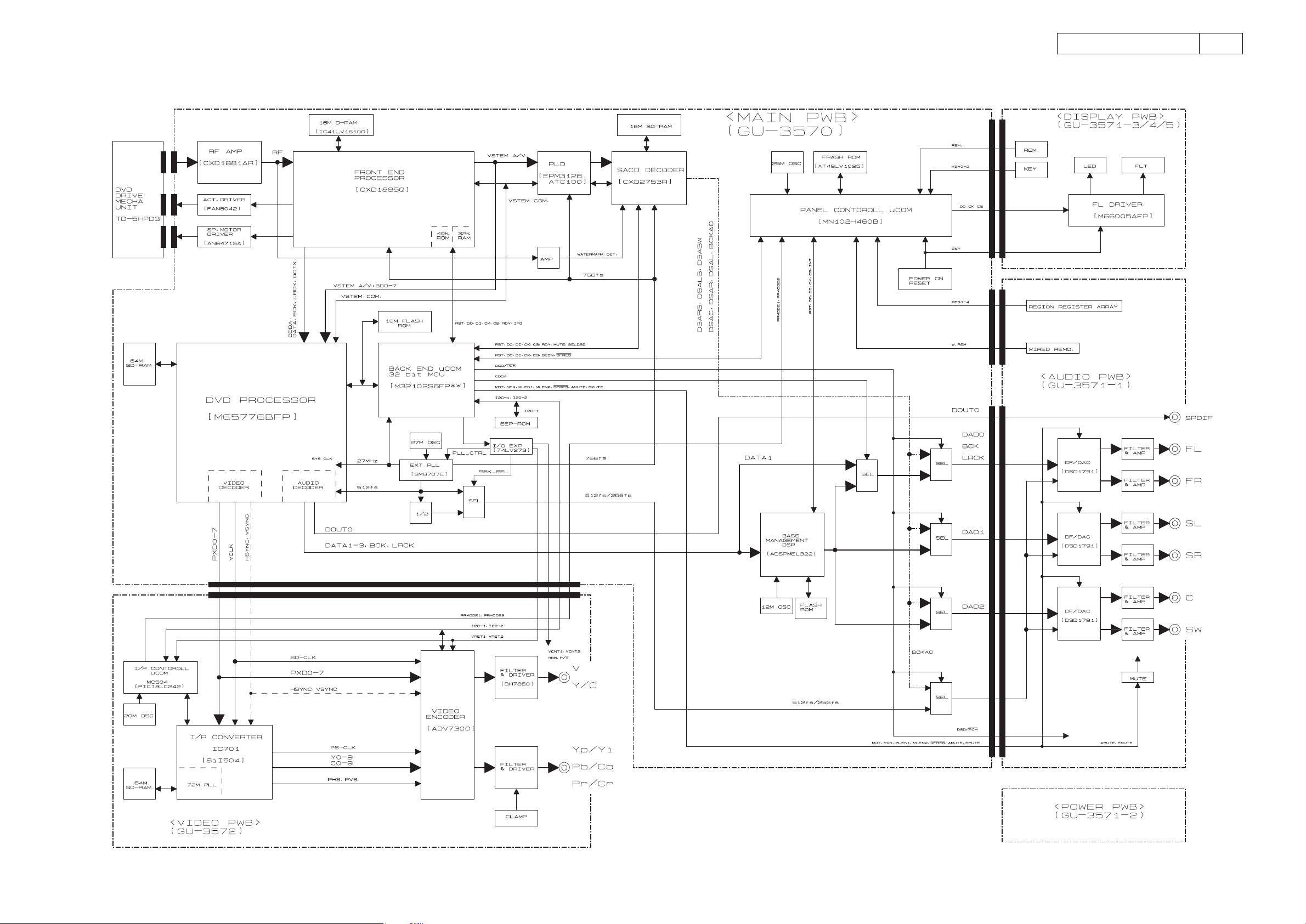
BLOCK DIAGRAM
DVD-2200
29
29
SEMICONDUCTORS
Only major semiconductrors are shown, general semiconducors etc. are omitted to list.
主な半導体を記載しています。汎用の半導体は記載を省略しています。
1. IC’s
Note: Abbreviation ahead of IC No. indicates the name of P.W.B., etc.
注 ): IC No. の前の記号は、基板の名称を表します。
MA: Main P.W.B.
AU: Audio/Power/Display P.W.B.
VI: Video P.W.B.
SC: Scart P.W.B.
CXD1885Q (MA: IC502)
Top View
DRAM I/F PWM.FG D/A
DVD-2200
30
18
DD
DV
RD9
RD10
RD11
RD12
RD13
RD14
RD15
RD0
RD1
157
DD33
DV
158
RD8
159
TEST0
160
TEST1
161
TEST2
162
TEST3
163
TEST4
164
TEST5
165
TEST6
166
TEST7
167
TEST8
168
TEST9
169
TEST10
170
TEST11
171
TEST12
172
TEST13
173
TEST14
174
TEST15
175
MODSEL0
176
MODSEL1
177
SS
DV
178
MODSEL2
179
GIO0
180
GIO1
181
GIO2
182
GIO3
183
DD33
DV
184
GIO4
185
GIO5
186
GIO6
187
GIO7
188
DV
DD18
189
GIO8
190
GIO9
191
GIO10
192
GIO11
193
GIO12
194
DV
SS
195
GIO13
196
GIO14
197
GIO15
198
GIO16
199
GIO17
200
GIO18
201
GIO19
202
TRST
203
TMS
204
TDI
JTAG Test/Monitor Pin
TDO
VMCHG
DVDD18
205
TCK
206
207
208
1 2 3 4 5 6 7 8 9 10 11 12 13 14 15 16 17 18 19 20 21 22 23 24 25 26 27 28 29 30 31 32 33 34 35 36 37 38 39 40 41 42 43 44 45 46 47 48 49 50 51 52
33
MA0
MA1
MA2
MA3
MA4
DD
ALCR
MSEL0
MSEL1
DV
MA5
RD2
MA6
RD3
MA7
RD4
MA8
SS
RD5
DV
MD0
TESTSEL
RD6
MD1
RD7
MD2
XMWR
MD3
XRAS
MD4
RA0
MD5
18
DD
DV
SS
DV
RA1
MD6
RA2
MD7
RA3
MALE
RA4
MCS
33
DD
DV
MWR
RA5
XSHD
DA2 (FSCON)
DA1 (SLED)
DCK
DRVIRQ
33
DD
DA0 (TSCON)
AV
105106107108109110111112113114115116117118119120121122123124125126127128129130131132133134135136137138139140141142143144145146147148149150151152153154155156
18
DD
DV
DRVRST
104
103
102
101
100
99
98
97
96
95
94
93
92
91
90
89
88
87
86
85
84
83
82
81
80
79
78
77
76
75
74
73
72
71
70
69
68
67
66
65
64
63
62
61
60
59
58
57
56
55
54
53
AV
DD18
VREFL
VREFH
AD9
AD8
AD7
AD6
AD5
AD4
AD3
AV
DD33
AD2
AD1
AD0
AVSS
AV
SS
RC
LPF2
LPF1
VCOI
AV
DD18
VFBC
CHG
JMOUT
JMREF
DD33
AV
IREF
TLC1
TLC0
HF
ATC
SS
AV
DTC
MIRRORH
HFD
RFOKGH
SCLKH
SO
SI
CSL
EXPLDT
EXVCO
BCK
LRCK
DOTK
DADT
C2PO
DRVRDY
DRVCLK
DRVRX
DRVTX
DV
DD33
A/DData PLL/Data SlicerASP S-I/O, Defect etcAudio D/AVSTEM I/F
SS
RA10
RA11
XMOE
XUCAS
XLCAS
GPWM5
GPWM4
GPWM3
GPWM2
GPWM1
GPWM0
SPWM2
VDT3
VDT2
VDT1
SPWM1FGAVSSDA3 (SLED2_TILT)
VDT0
HDRQ
VSTEM I/FClockB/E MCU I/F
VEFG
XHAC
RA6
RA7
RA8
RA9
DV
XI
SS
33
DD
DV
MRD
18
DD
MINT
MRDY
SYSCK
DV
SS
XO
DV
DV
VDT7
VDT6
VDT5
VDT4
30
 Loading...