

Page 1
AVR-2800
NEW MODEL INFORMATION
Outstanding surround sound an affor dable price,with Dolby Digital and DTS decoding.
Featuring the latest in Dolby Digital and DTS decoding technology, theAVR-2800 provides outstanding home theater surround
sound performance. The heart of the AVR-2800 is Denon’s Dynamic Discrete Surround Circuit-Digital technology, incorporating
high performance dual DSP chips and superior A/D and D/A conversion devices. This provides superb listening results, with virtually any
home theater or music source. Prepared for the future, the AVR-2800 features 6-Channel external input, for connection to future
multi-channel surround formats. A high quality, discrete power output section provides a total system power of 425 watts RMS into
8 ohms. Full 24 bit, 96 kHz digital-to-analog D/A converters on all 6 channels (3 stereo pairs) provide transparent reproduction of
multi-channel music and motion picture soundtracks with outstanding dynamic range and superb low level resolution. Outstanding
surround sound an affordable price, with Dolby Digital and DTS decoding. The AVR-2800’s remote controller features an easy-touse layout where most frequently used buttons are provided in different colors and shapes for easy recognition, even while keeping
your eyes on the screen. The buttons also feature “Self-illuminated GLO-KEY” for easy operation in the dark.
Dolby Digital and DTS A/V Receiver
■ Equal Power Discrete Power Amplifier
Front 85 W + 85 W (8 ohms, 20Hz - 20kHz, 0.05% THD)
Center 85 W (8 ohms, 20Hz - 20kHz, 0.05% THD)
Surround 85 W + 85 W (8 ohms, 20Hz - 20kHz, 0.05% THD)
All five power amplifier channels feature discrete power output devices, and all five amplifier channels provide equal
power with lowest distortion. Each channel is rated at 85 watts,
into 8 ohms, from 20 Hz - 20 kHz, with no more than 0.05%
THD. A hallmark of Denon A/V component design, the equal
power amplifier provides outstandingly accurate reproduction of
motion picture soundtracks and multi-channel music programs.
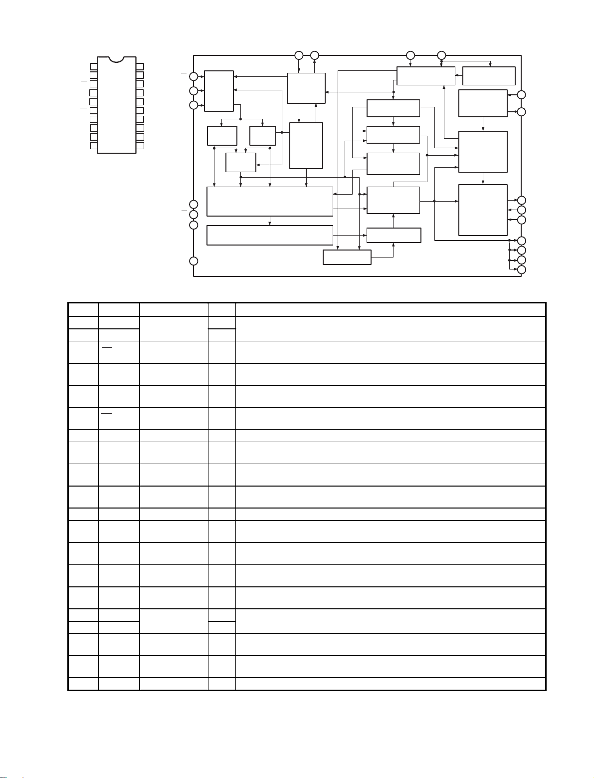
■ DDSC-Digital (Dynamic Discrete Surround
Circuit-Digital)
Since surround signals are all processed in the digital domain,
the AVR-2800 is equipped with a newly-developed, sophisticated, high-performance dual DSP circuit for the Dolby Digital, Dolby
Pro Logic, dts decoders, and Surround Simulator.The D/Aconverters feature high resolution designs for all the Front L/R,
Center, Surround L/R, and Subwoofer channels.This combination of DSP and D/A converters works to bring out the tremendous potential of Dolby Digital and dts sound. In addition, high
resolution A/D converters have been incorporated for the Dolby
Pro Logic decoder.The high sound quality of New DDSC-Digital
is due in part to the high-grade signal processing of the 24-bit,
96-kHz Digital Interface Receiver (DIR). The AVR-2800 not only
allows digital signals input from DVD and other advanced media
to pass directly to the DIR, it also processes them while preserving their integrity so that even the most delicate nuances of the
music, reflecting the emotions of the artists, are passed unfettered to the dual digital signal processors (DSP).
Dynamic Discrete Surround Circuit-Digital Block Diagram
Page 2

■ Dolby Digital
Dolby Digital and Dolby Pro Logic decoding functions are performed in the digital domain for excellent dynamic range and
crystal clear reproduction.
■ DTS
Digital Theater Systems decoding provides thrilling movie and
music multi-channel surround sound.
■ 96kHz, 24-bit Audio D/A Converters
■ 6-Channel External Input For Future Multi-Channel Formats
■ Separate Current Supplies for Circuits
The AVR-2800 is equipped with a main transformer featuring
independent 5-winding outputs, and a dedicated transformer for
the microprocessor, to completely separate the power amplifier,
audio, digital, video, and display circuits. This construction
reduces noise interference among the circuits and ensures a
clean, transparent sound.
■ Hefty Power Transformer for Stable Supply of Power
A power transformer has been connected in the power section where it is combined with a rectifier diode and a large block
capacitor to ensure a large, stable supply of electrical current.
Accordingly, the AVR-2800 boasts high output power of 85 W for
each of the 5 channels.
■ Stable Speaker Drive
In the AVR-2800, the circuitry through which current flows
to drive the speakers has been incorporated onto a single
board between the rectifier circuit of the power source and the
speaker terminals. Anew phase correction circuit has also
been adopted, eliminating the need for an output coil. Since
this configuration allows the power transistor to drive the
speakers directly, there is no loss of power to any of the
channels. The sound that you hear is thus extremely stable
as well as powerful.
■ Pre Outputs for System Upgrading
The pre-out terminals on the AVR-2800 is offered for Front L/R,
Center and Mono (Subwoofer) channels. Aseparate power amp
can be connected to these terminals to upgrade your system.
■ Video Select Switch
This function lets you select video sources independently of
the audio sources.
■ All-channel Level Control
■ Binding Post Speaker Terminals for All Channels
■ Icon-based On-Screen Display
The AVR-2800 provides an On-Screen Display (OSD) featuring icons (pictorial representations) to let you easily monitor
the current operating status.
■ Personal Memory Plus
The handy Personal Memory Plus function allows you to
store the surround mode, the level settings for all speakers,
as well as the delay time, to further customize the sound
source. Simply push any source button and it will instantly
display the settings stored for that source.
■ Multi-function Remote Controller
● Self-illuminated GLO-KEY Remote Controller with Easy
Recognition Layout
● System Call Function to execute up to 10 successive pre-assigned
commands at the single touch of a button
● Pre-Memory and Programming Function for non-DENON components
■ Frequency Synthesis Tuning
● 40-Station AM/FM Random Preset Memory Tuning
● Auto Preset Memory
■ Other Features
● Cinema Equalizer
● Music Surround Modes Including 5-channel Stereo
● “S”and Composite Video Switching
● Front A/B Speaker Switching
Connect another pair of stereo speakers in another room.
● Tone Control
● 2 Switched AC Outlets
■ Input/Output Terminals For Every A/V System
● Audio Inputs
3 Digital (Optical) Input ....... OPTICAL x 3
1 Digital (Coaxial) Input ...... COAXIAL x 1
9 Analog Inputs ................... PHONO, CD, TUNER, DVD, VDP,
TV/DBS, VCR-1, VCR-2/V-AUX,
MD/TAPE
6 Analog EXT. Inputs ........... FRONT L/R, CENTER,
SURROUND L/R, SUBWOOFER
● Audio Outputs
4 Analog Pre Outputs ......... FRONT L/R, CENTER, SUBWOOFER
3 Analog Rec Outputs ........ VCR-1, VCR-2/V-AUX, MD/TAPE
● Video Inputs
5 S-Video Inputs ................. DVD, VDP, TV/DBS, VCR-1,
VCR-2/V-AUX
5 Composite Inputs ............. DVD, VDP, TV/DBS, VCR-1,
VCR-2/V-AUX
● Video Outputs
3 S-Video Outputs .............. VCR-1, VCR-2/V-AUX, MONITOR
3 Composite Outputs .......... VCR-1, VCR-2/V-AUX, MONITOR
Specifications
■ Power Amplifier Section
Rated output *THD figures are power amp stage values.
Front...........................................85 W + 85 W (8 ohms, 20Hz - 20kHz, 0.05% THD)
Center........................................ 85 W (8 ohms, 20Hz - 20kHz, 0.05% THD)
Surround................................... 85 W + 85 W (8 ohms, 20Hz - 20kHz, 0.05% THD)
■ Preamplifier Section
Input sensitivity/Impedance
PHONO(MM)............... 2.5 mV/47 kohms
CD, DVD, VDP, TV/DBS, VCR-1 VCR-2/V-AUX, MD/TAPE,
FRONT L/R, CENTER, SURROUND L/R,
SUBWOOFER............. 200 mV/47 kohms
Output level/Load Impedance
FRONT L/R, CENTER,
SUBWOOFER............. 1.2 V/10 kohms
VCR, MD/TAPE,
MONITOR .................... 200 mV/47 kohms
RIAA deviation................. ±1 dB (20 Hz - 20 kHz)
Tone control..................... Treble: ±10 dB at 10 kHz
Bass: ±10 dB at 100 Hz
■ FM Section
Tuning frequency range... 87.50 - 107.90 MHz
Usable sensitivity............. 1.0 µV (11.2 dBf)
■ AM Section
Tuning frequency range... 520 - 1710 kHz
Usable sensitivity............. 18 µV
■ General
Power supply................... AC 120 V, 60 Hz
Power consumption......... 5.0 A
Dimensions...................... 434 (W) x 171 (H) x 416 (D) mm
17.1” (W) x 6.7”(H) x 16.4”(D)
Weight.............................. 11.5 kg, 25.4 lbs
*Design and specifications are subject to change without notice.
*”Dolby”, “Dolby Digital”, “Pro Logic”, and the double-D device are registered trademarks of
Dolby Laboratories Licensing Corporation.
*DTS is registered trademarks of DTS Technology.
DENON ELECTRONICS. NIPPON COLUMBIA CO., LTD.
DIVISION OF DENON CORPORATION (USA) 14-14, AKASAKA4-CHOME, MINATO-KU, TOKYO 107-8011, JAPAN
222 NEW ROAD, PARSIPPANY, NEW JERSEY 07054, USA Denon Home Page Address: http://www.denon.co.jp
TEL: 973-396-0810 www.del.denon.com
DENON CANADA INC.
17 DENISON STREET, MARKHAM ONTARIO, CANADAL3R 1B5
TEL: 905-475-4085 11790699 A Printed in Japan
Page 3

SAFETY PRECAUTIONS
The following check should be performed for the continued protection of the customer and service technician.
LEAKAGE CURRENT CHECK
Before returning the unit to the customer, make sure you make either (1) a leakage current check or (2) a line to chassis
resistance check. If the leakage current exceeds 0.5 milliamps, or if the resistance from chassis to either side of the
power cord is less than 460 kohms, the unit is defective.
SPECIFICATIONS
AUDIO SECTION
Power Amplifier
Rated output: Front: 90W + 90W (8Ω/ohms, 20Hz ~ 20kHz with 0.05% T.H.D.)
Center: 90W (8Ω/ohms, 20Hz ~ 20kHz with 0.05% T.H.D.)
Surround: 90W + 90W (8Ω/ohms, 20Hz ~ 20kHz with 0.05% T.H.D.)
Surround Back: 90W (8Ω/ohms, 20 Hz ~ 20kHz with 0.05% T.H.D.)
Dynamic power: 120W × 2ch (8Ω/ohms)
Output terminals: Front: A or B 6 ~ 16Ω/ohms
Analog
Input sensitivity/input impedance: 200mV/47kΩ/kohms
Frequency response: 10Hz ~ 100kHz: +0, −3dB (DIRECT mode)
S/N: 102dB (DIRECT mode)
Distortion: 0.005% (20Hz ~ 20kHz) (DIRECT mode)
Rated output: 1.2V
Digital
D/A output: Rated output ⎯ 2V (at 0dB playback)
Digital input: Format ⎯ Digital audio interface
Phono equalizer (PHONO input
Input sensitivity: 2.5mV
RIAA deviation: ±1dB (20Hz to 20kHz)
Signal-to-noise ratio: 74dB (A weighting, with 5mV input)
Rated output/Maximum output: 150mV/7V
Distortion factor: 0.03% (1kHz, 3V)
VIDEO SECTION
Standard video jacks
Input/output level and impedance: 1Vp-p, 75Ω/ohms
Frequency response: 5Hz ~ 10MHz ⎯ +0, −3dB
S-video jacks
Input/output level and impedance: Y (brightness) signal ⎯ 1Vp-p, 75Ω/ohms
Frequency response: 5Hz ~ 10MHz ⎯ +0, −3dB
Color component video jacks
Input/output level and impedance: Y (brightness) signal ⎯ 1Vp-p, 75Ω/ohms
Frequency response: 5Hz ~27MHz ⎯ +0, −3dB
TUNER SECTION
Receiving Range: 87.50MHz ~ 107.90MHz 520kHz ~ 1710kHz
Usable Sensitivity: 1.0μV (11.2dBf) 18μV
50dB Quieting Sensitivity: MONO: 1.6μV (15.3dBf)
S/N (IHF-A): MONO: 77dB
Total Har monic Distortion (at 1kHz): MONO: 0.15%
GENERAL
Power supply: AC120V, 60Hz (for U.S.A., Canada and Taiwan R.O.C. models)
Power consumption: 5.0A (for U.S.A.& Canada model)
Maximum external dimensions: 434 (W) × 171 (H) × 416 (D)mm (17-3/32″× 6-11/32″× 16-3/8″)
Weight: 11.5kg (25 lbs 6 oz)
REMOTE CONTROL UNIT
Batteries: R6P/AA Type (three batteries)
External dimensions: 70 (W) × 215 (H) × 24 (D)mm (2-3/4″× 8-15/32″× 15/16″)
Weight: 200g (Approx. 7 oz) (including batteries)
* For purposes of improvement, specifications and design are subject to change without notice.
170W × 2ch (4Ω/ohms)
200W × 2ch (2Ω/ohms)
Center, Surround, Surr.Back: 6 ~ 16Ω/ohms
Total har monic distortion ⎯ 0.008% (1 kHz, at 0 dB)
S/N ratio ⎯ 102dB
Dynamic range ⎯ 96dB
⎯⎯
⎯ REC OUT)
⎯⎯
C (color) signal ⎯ 0.286Vp-p, 75Ω/ohms
P
B/CB (blue) signal ⎯ 0.7Vp-p, 75Ω/ohms
P
R/CR (red) signal ⎯ 0.7Vp-p, 75Ω/ohms
[FM] (note: μV at 75Ω/ohms, 0dBf=1 × 10
(for U.S.A., Canada and multiple voltage models) (for U.S.A., Canada and Multiple voltage models)
87.50MHz ~ 108.00MHz 522kHz ~ 1611kHz
(for Europe, Asia, China, Hong Kong, Taiwan R.O.C. and Multiple voltage models) (for Europe, Asia, China, Hong Kong, Taiwan R.O.C. and multiple voltage models)
STEREO: 23μV (38.5dBf)
STEREO: 72dB
STEREO: 0.3%
AC230V, 50Hz (for Europe model)
AC220V, 50Hz (for China model)
AC115V/230V, 50/60Hz (for Asia, Hong Kong and Multiple voltage models)
270W (for Europe, Asia, China, Hong Kong and Multiple voltage models)
650W (for Taiwan R.O.C. model)
2.0W Max (Standby)
(RC-903: for U.S.A., Canada, Asia, China, Hong Kong, Taiwan R.O.C. and Multiple voltage models)
(RC-904: for Europe model)
135W + 135W (6Ω/ohms, 1kHz with 0.7% T.H.D.)
150W + 150W (6Ω/ohms, EIAJ)
135W (6Ω/ohms, 1kHz with 0.7% T.H.D.)
150W (6Ω/ohms, EIAJ)
135W + 135W (6Ω/ohms, 1kHz with 0.7% T.H.D.)
150W + 150W (6Ω/ohms, EIAJ)
135W (6Ω/ohms, 1kHz with 0.7% T.H.D.)
150W (6Ω/ohms, EIAJ)
A + B 8 ~ 16Ω/ohms
-15
W) [AM]
2
Page 4
WIRE ARRANGEMENT
If wire bundles are untied or moved to perform adjustment or parts replacement etc.,be sure to rearrange them neatly as they
were originally bundled or placed afterward.
Otherwise, incorrect arrangement can be a cause of noise generation.
Wire arrangement viewed from the top
3
Page 5
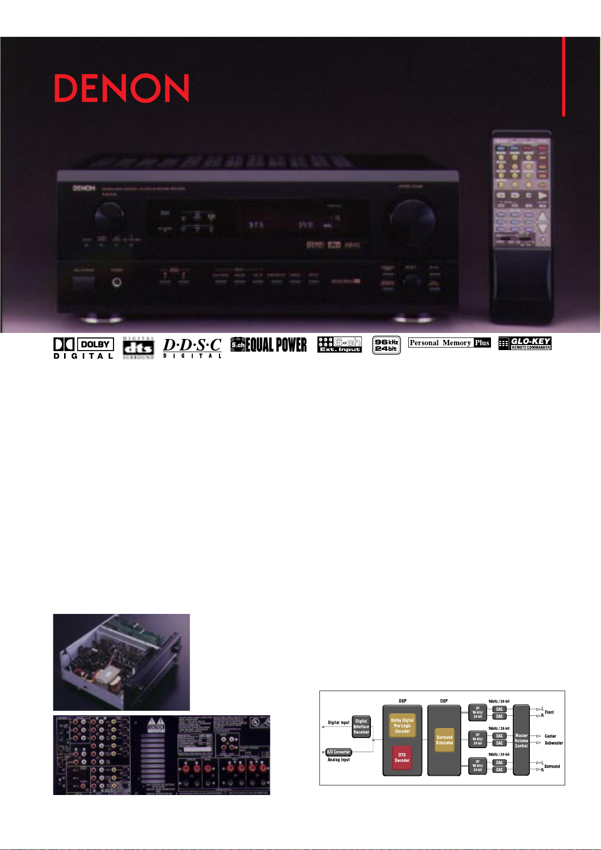
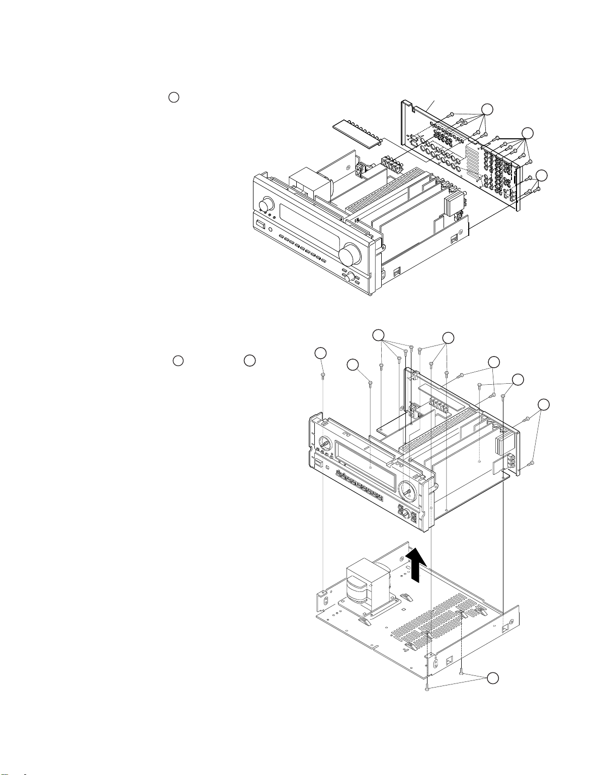
DISASSEMBLY
(Follow the procedure below in reverse order when reassembling)
1. Top Cover
Remove 3 screws 1 on the rear and 6 screws 2 on both
sides to detach the Top Cover as shown in the arrow
direction.
2
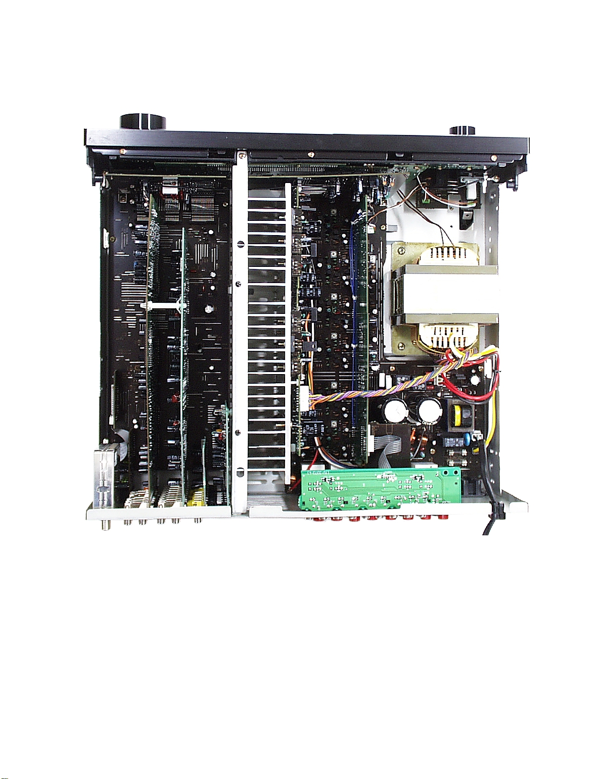
2. Front Panel
(1) Remove 7 screws 3 from the top and bottom edges of
the Front Panel.
(2) Release 4 top and bottom hooks, then detach the Front
Panel as shown in the arrow direction.
Top Cover
1
2
3
Hook
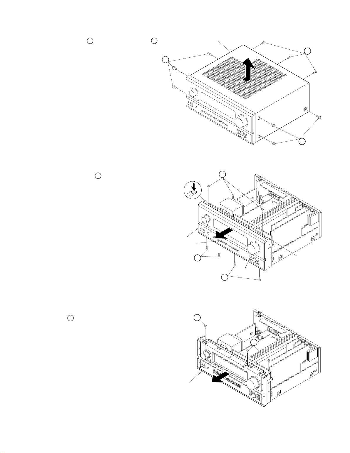
3. Inner Panel
Pull out the Inner Panel in the arrow direction after removing
3 screws
.
4
Front Panel
Inner Panel
Hook
3
Hook
3
4
4
Hook
4
Page 6
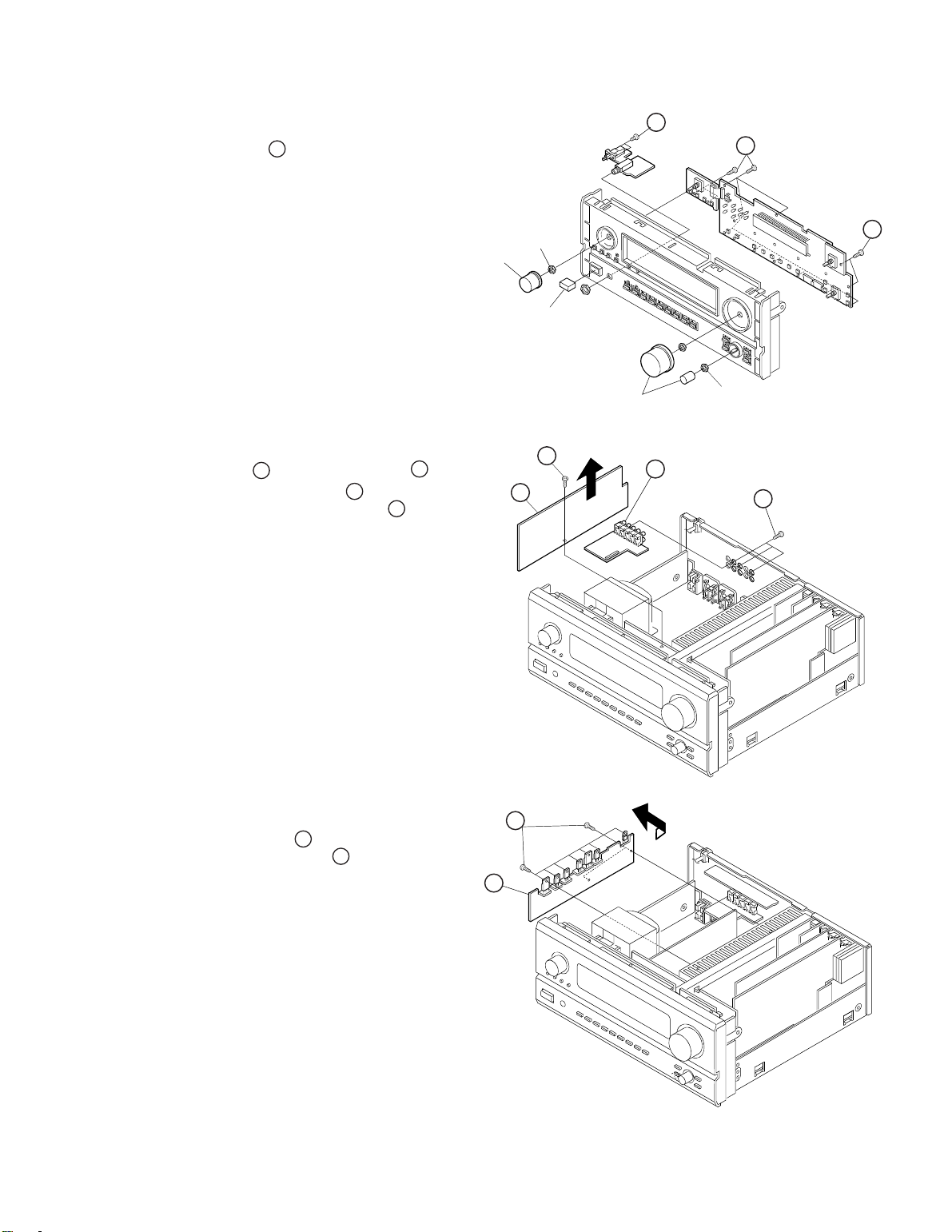
4. Inner Panel Ass'y
(1) Remove 3 round and 1 square knobs, and unscrew 4
nuts.
(2) Remove 15 screws
fixing each P.W.B.
5
5
5
5. Amp Connect Unit
(1) Remove 3 screw to detach Pre-out Unit .
(2) Take off the Amp Connect Unit as shown in the
arrow direction after removing 1 screw .
6
8
9
7
Round Knob
Square Knob
Nut
Round Knob
Nut
5
9
7
8
6
6. Regulator Unit
Take off the Regulator Unit as shown in the arrow
direction after removing 9 screws .
5
Page 7
7. Component-Video/S-Video / C-video /
Audio & DSP / Ext-in VR / Digital-in / AM
FM Tuner Unit
(1) Remove 44 screws to detach the Rear Panel.
(2) Take off the objective P.W.B. upward.
Rear Panel
8. How to Check Power / Control Unit with
Power-on
(1) Remove 13 screws ,and 4 screws fixing to the
Chassis.
(2) Pull up the Unit to separate from the Chassis.
!
"
!
!
!
!
"
!
"
!
6
Page 8
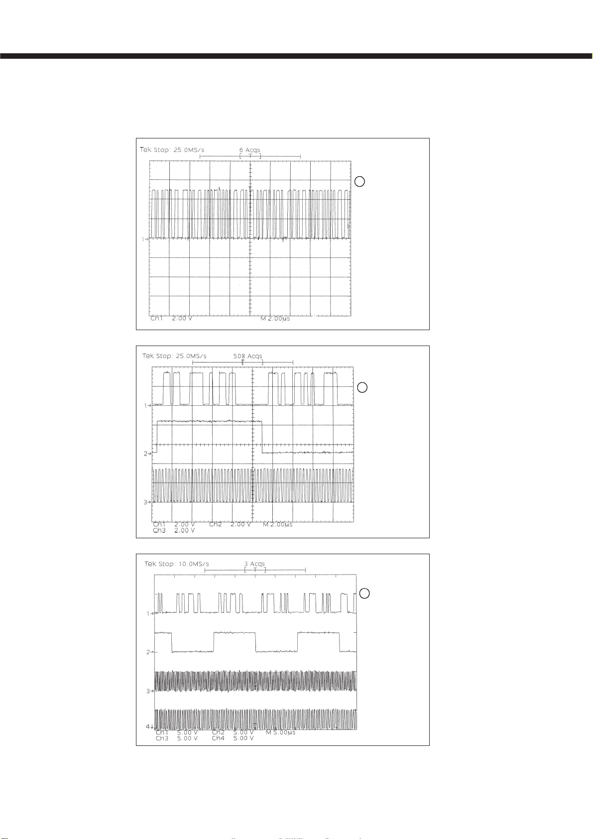
CLOCK FLOW & WAVE FORM IN DIGITAL BLOCK
Wave Form
1
CH1: D-DATA
AVR-2802/982
(IC505 (5) )
2
CH1: DATA
CH2: DA-LRCK(fs)
CH3: DA-SCK(64fs)
3
CH1: DATA
CH2: fs
CH3: 64fs
CH4: 256fs
7
Page 9
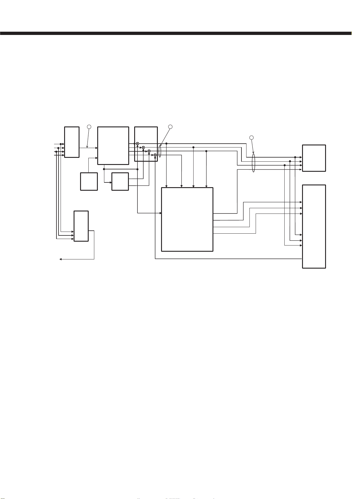
Clock Flow
AVR-2802/982
COAXIAL
OPTICAL-1
OPTICAL-2
OPTICAL-3
OPTICAL
OUTPUT
INPUT
SELECTOR
IC505
SN74HC
151NS
(15)
(14)
(5)
(13)
(12)
(3)
(2)
(1)
12.288MHz
IC506
SN74HC
151NS
1
X801
(5)
DIR
IC800
LC89055W
(5)DIN2
XIN(22)
XMCK(20)
SN74LV4040APW
CKOUT(13)
BCK
(14)
LRCK(15)
(16)
DATA
IC813
(10)
(13)
(7)
A/D SELECTOR
IC804
74LVX157
256fs
64fs
fs
DATA
2
MCLK
DA SCK
DA LRCK
SD IN
(44) (22) (25) (26)
MCLK
SDATAN1
(27) (43) (42)
(30)CLKIN
CS493292
* fs is a sampling frequency of input digital signal.
e.g.:sampling frequency 48kHz fs=48kHz
* 64fs and 256fs are 64 or 256 times the sampling frequency respectively.
e.g.: sampling frequency 48kHz
64fs: 48kHz x 64=3.072MHz
256fs: 48kHz x 256=12.288MHz
* The sampling frequency for analog input is fixed to 48kHz internally.
* (No.) indicates the pin number of individual.
* The arrow indicates the direction of signal as the input terminal pointed by
the arrow and the output terminal by the opposite.
SCLKN1 LRCKN1
SCLK LRCLKCMPDAT
AUDATA0 (41)
AUDATA2 (39)
AUDATA1 (40)
XMT958 (3)
IC814
DSP
3
256fs
64fs
fs
FRONT
CENTER/SW
SURROUND
SURROUND BACK
D/A CONVERTER
IC801
AD1854
(2)256fs
(26)64fs
(25)fs
(27)DATA
CODEC
IC602
AK4527
(6)SDTI1
(7)SDTI2
(8)SDTI3
(39)MCLK
(4)BICK
(5)LRCK
(9)SDTO
8
Page 10
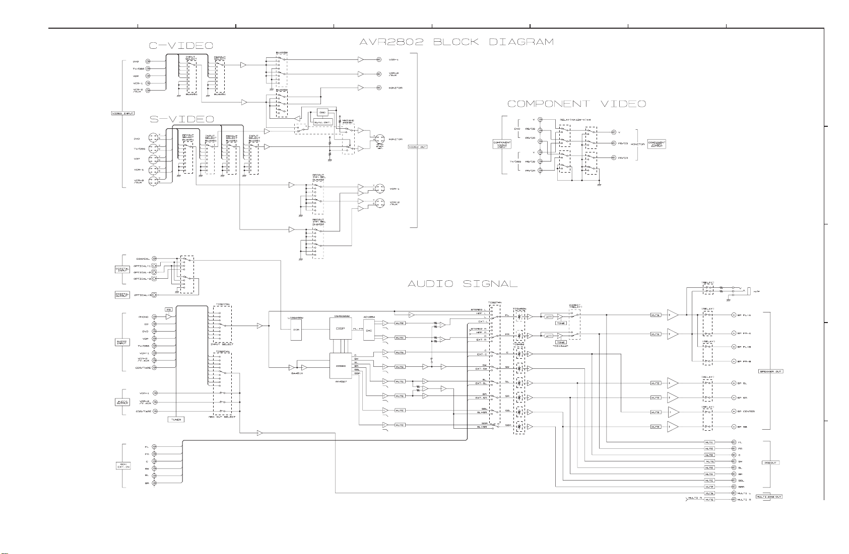
BLOCK DIAGRAM
1
2
3
4
5
76
8
A
B
C
D
E
9
Page 11
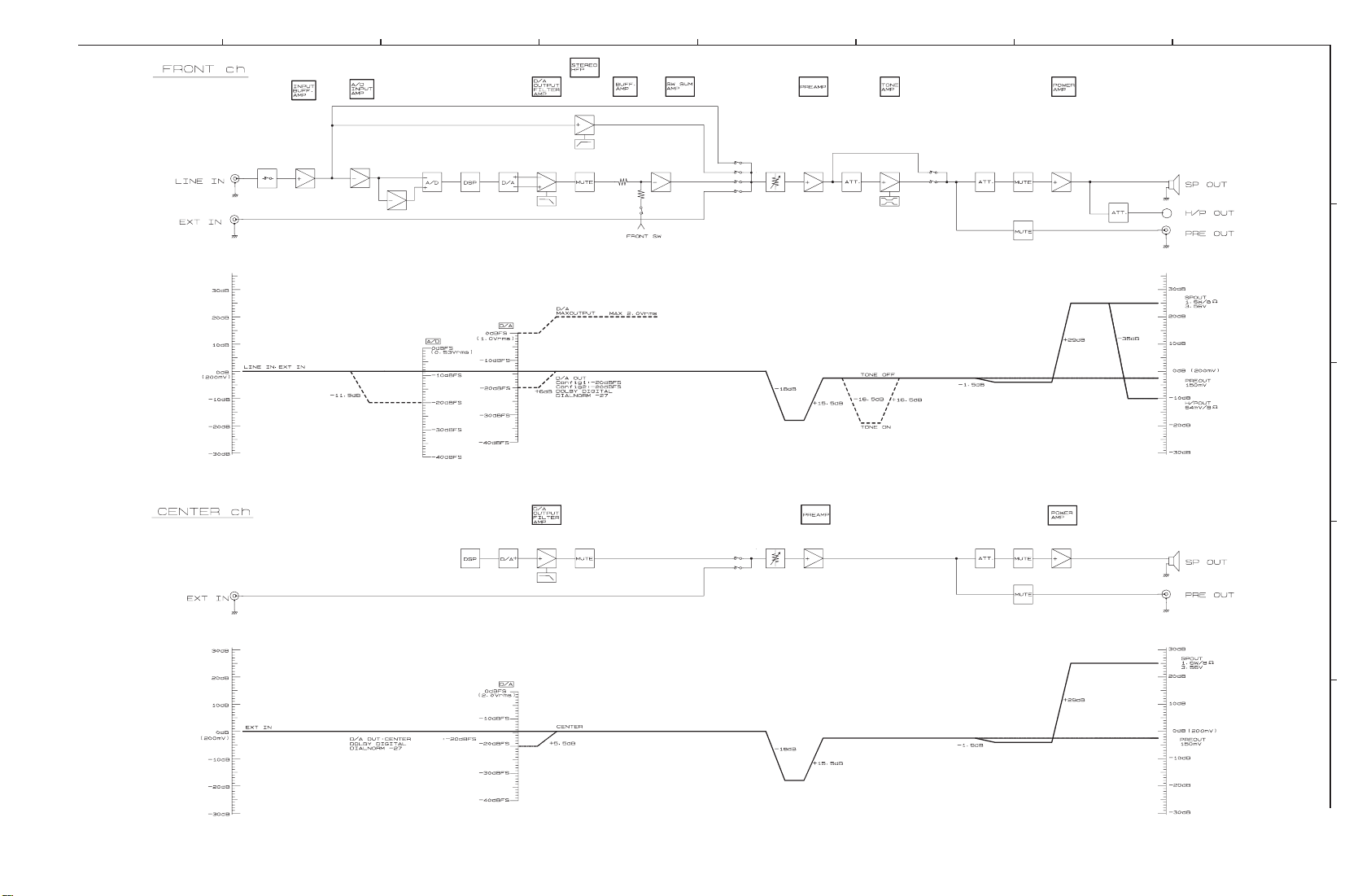
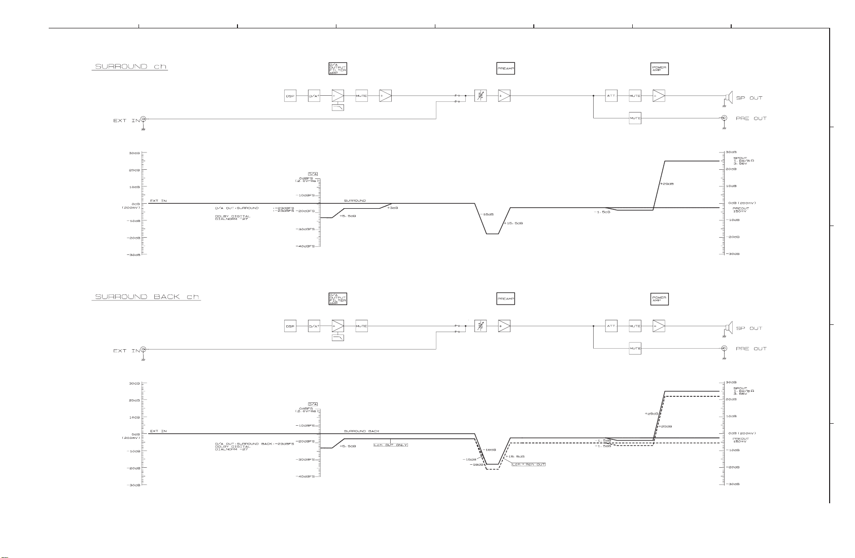
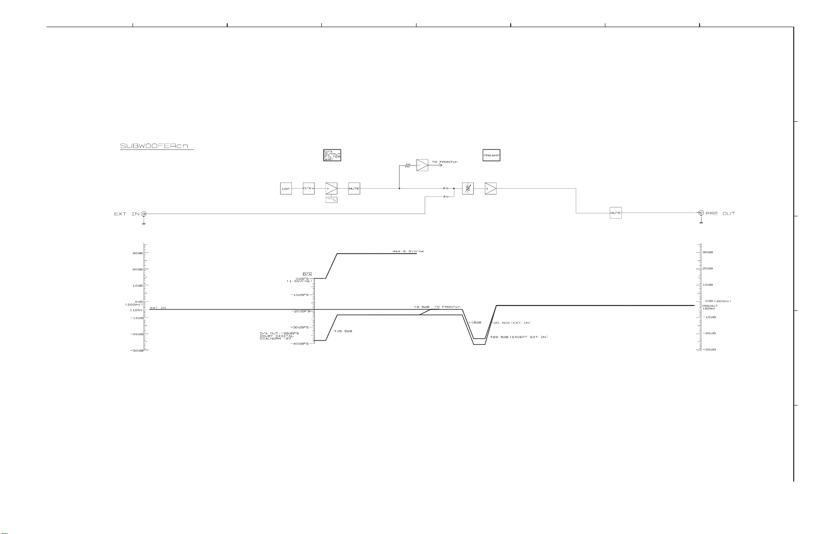
LEVEL DIAGRAMS (1/3)
1
2
3
4
5
76
8
A
B
C
D
E
10
Page 12
LEVEL DIAGRAMS (2/3)
1
2
3
4
5
76
8
A
B
C
D
E
11
Page 13
LEVEL DIAGRAMS (3/3)
1
2
3
4
5
76
8
A
B
C
D
E
12
Page 14
AVR-2802/982
CAUTION IN SERVICING
Initializing AV SURROUND RECEIVER
AV SURROUND RECEIVER initialization should be performed when the μcom, peripheral parts of μcom, and DSP
P.W.B. are replaced.
1. Switch off the unit and remove the AC cord from the
wall outlet.
2. Hold the following A button and B button, and plug
the AC cord into the outlet.
3. Check that the entire display is flashing with an
interval of about 1 second, and release your fingers
from the 2 buttons and the microprocessor will be
initialized.
Note: If step 3 does not work, start over from step 1.
All user settings will be lost and its factory setting will be recovered when this initialization mode.
So make sure to memorize your setting for restoring after the initialization.
REMOTE
SIGNAL
SENSOR
LOCK
DIGITAL
INPUT
STAND BY
AUTO
PCM
DIGITAL
2
VOLUME LEVEL
13
Page 15
ADJUSTMENT
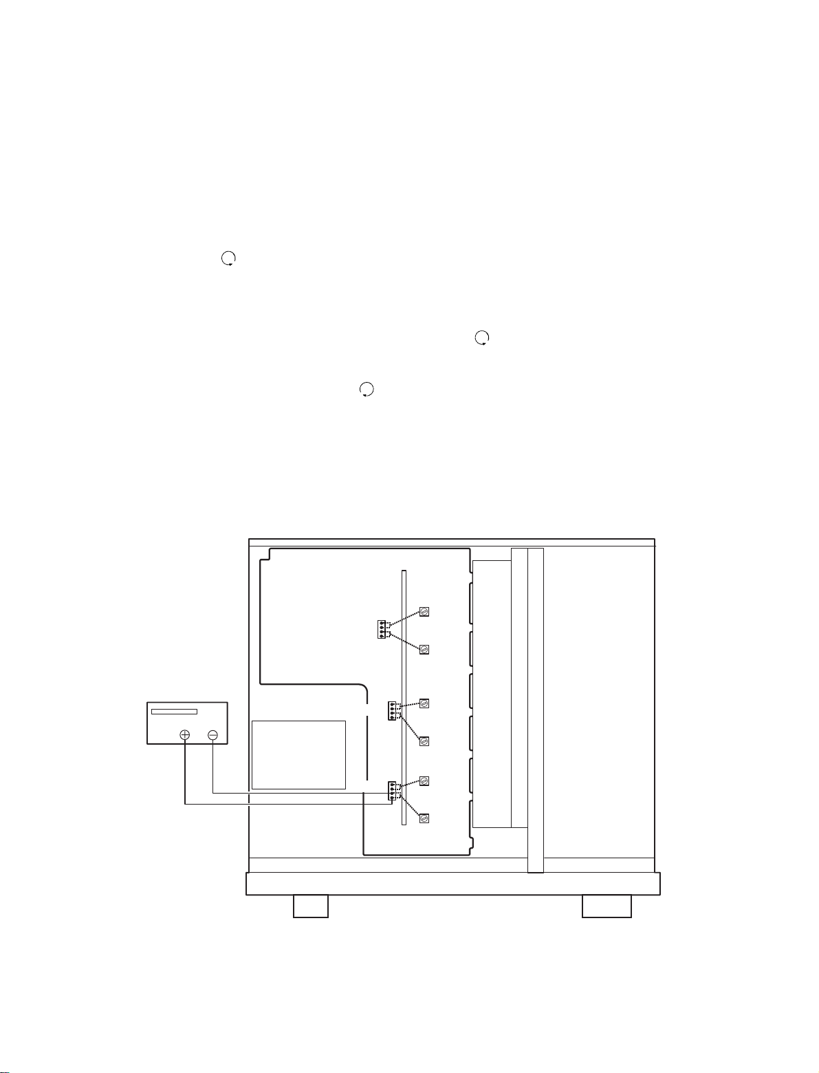
Idling Current (1U-3368-1)
Required measurement equipment : DC Voltmeter
Preparation
(1) Avoid direct blow from an air conditioner or an electric fan, and adjust the unit at normal room tempereture 15 °C ~ 30 °C
(59 °F ~ 86 °F).
(2) Presetting
POWER (Power sourse switch) → OFF
SPEAKER (Speaker terminal) → No load (Do not connect speaker, dummy resistor, etc.)
Adjustment
(1) Remove top cover and set VR101, VR102, VR201, VR202, VR301, VR401, on 1U-3368-1 (Power Unit) at fully
counterclockwise (
(2) Connect DC Voltmeter to test points (FRONT-Lch: TP101, FRONT-Rch: TP102, CENTER ch: TP103, SURROUND-Lch:
TP101, SURROUND-Rch: TP103, SURROUND BACK-ch: TP102).
(3) Connect power cord to AC Line, and turn power switch "ON".
).
(4) Presetting. MASTER VOLUME : "---" counterclockwise (
min.)
MODE : 6CH STEREO
FUNCTION : CD
(5) Allow 2 minutes, and turn VR101 clockwise (
) to adjust the TEST POINT voltage to 6.5 mV ±0.5 mV DC.
(6) After 10 minutes from preset, turn VR101 to set the voltage to 8 mV ±0.5 mV DC.
(7) Adjust the Variable Resistors of other channels in the same way.
(8) After 5 minutes from (6), turn VR101 to set the voltage to 8 mV ±0.5 mV DC.
(9) Adjust the Variable Resistors of other channels in the same way.
VR301
VR102
VR401
VR202
DC Voltmeter
SBch
TP102
FRch
Cch
TP103
SRch
TP101
FLch
SLch
VR101
VR201
14
Page 16
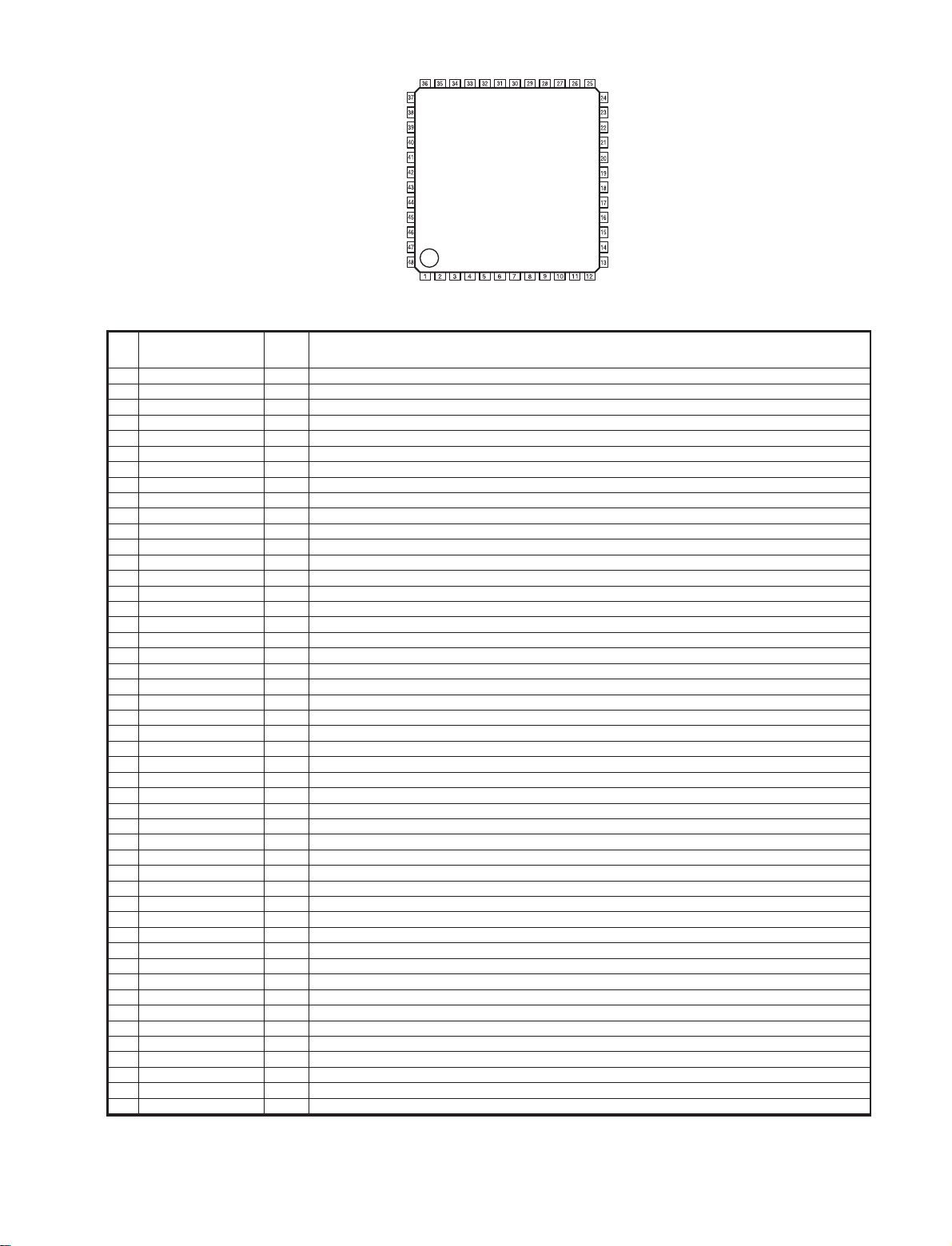
SEMICONDUCTORS
IC’s
Note: Abbreviation ahead of IC No. indicates the name of P.W.B.
PO: Power P.W.B. RE: Regulator P.W.B.
EX: Exit in P.W.B. AU: Audio/DSP P.W.B.
CO: Control P.W.B.
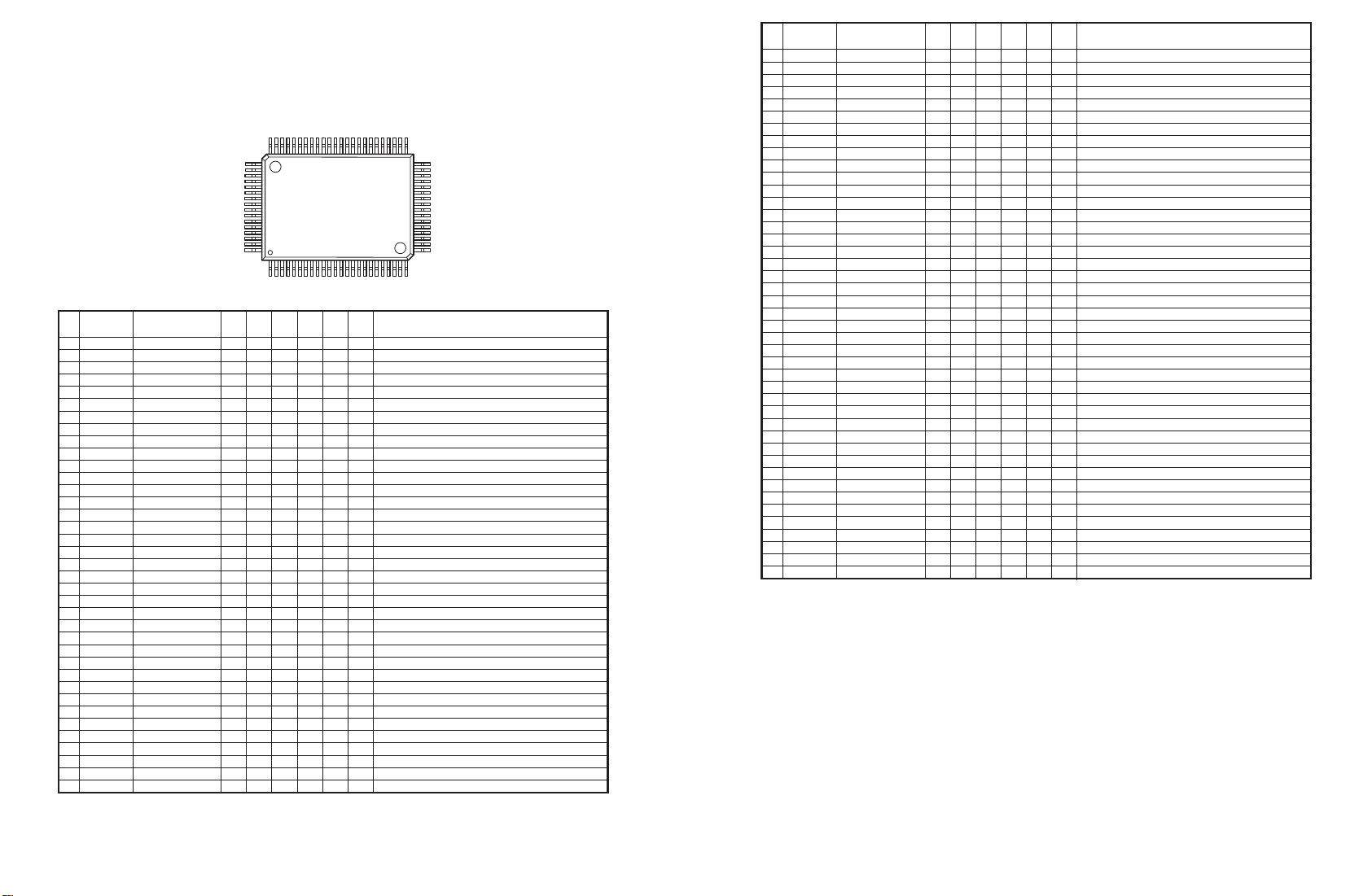
TMP88CU74F
(CO: IC303)
64
65
80
124
TMP88CU74F Terminal Function
Pin
Name
No.
1 P02/S01 RDS RESET O C ⎯⎯ Z L RDS reset output (LC72720)
2 P03 OSD RST O C ⎯⎯ Z H OSD control output (M35015)
3 P04 PLL DATA I ⎯⎯⎯⎯⎯PLL Serial data input terminal (LC72131)
4 P05 PLFLRDS DATA O C ⎯⎯ ZL
5 P06 PLL STB O C ⎯⎯ Z L PLL control terminal (LC72131)
6 P07 PLFLRDS CLK O C ⎯⎯ ZL
7 Vss Vss I ⎯ GND ⎯⎯ L GND
8 Xout Xout O ⎯⎯⎯⎯⎯XTAL
9 Xin Xin I ⎯⎯⎯⎯⎯XTAL
10 RESET_ RESET_ I ⎯ Eu Lv L ⎯ Reset input
11 P22/XTOUT TUNED_ I ⎯ Eu Lv Z ⎯ Tuning detect, L: Tuned
12 P21/XTIN STEREO_ I ⎯ Eu Lv Z ⎯ L: At stereo receive
13 TEST TEST I ⎯ GND S ⎯⎯Connect to GND
14 P20/INT5_ B.DOWN_ I ⎯ Eu Lv Z ⎯ Power down detect, L: Power down
15 P10/INT0_ PROTECT_ I ⎯ Ed E&L Z ⎯ PROTECTION detect input, H: Detect
16 P11/INT1 RDS DATA I ⎯⎯⎯ Z L RDS data input (LC72720)
17 P12 OSD CLK O C ⎯⎯ Z H OSD control output (M35015)
18 P13 OSD CS O C ⎯⎯ Z H OSD control output (M35015)
19 P1 4 OSD DATA O C ⎯⎯ Z L OSD control output (M35015)
20 P15/INT3 REMOCON I ⎯ Ed E&L Z ⎯ Remote control signal input
21 P16/INT2 ACK O C ⎯⎯ Z L MAIN-SUB CPU comm. control terminal
22 P17/INT4 REQ I ⎯ Eu ⎯ Z L MAIN-SUB CPU comm. control terminal
23 P30/SCL SI I MAIN-SUB CPU comm. control terminal
24 P31/SDA SO O C MAIN-SUB CPU comm. control terminal
25 P32/SCK0_ CLK O C MAIN-SUB CPU comm. control terminal
26 P40/AIN0 MODE I ⎯ Eu Lv Z ⎯ Destination switching input
27 P41/AIN1 KEY1 I ⎯ Eu Lv Z ⎯ Button input 1
28 P42/AIN2 KEY2 I ⎯ Eu Lv Z ⎯ Button input 2
29 P43/AIN3 KEY3 I ⎯ Eu Lv Z ⎯ Button input 3
30 P44/AIN4 FUNC STB1 O C ⎯⎯ ZL
31 P45/AIN5 FUNC/T. CON CLK O C ⎯⎯ ZL
32 P46/AIN6 FUNC/T. CON DATA O C ⎯⎯ ZL
33 P47/AIN7 E.VOL STB4 O C ⎯⎯ Z L Elect. volume control output (TC9482)
34 P50/AIN8 E.VOL STB1 O C ⎯⎯ L L Elect. volume control output (TC9459)
35 P51/AIN9 TONE STB O C ⎯⎯ L L TONE control output (TC9184P)
36 P52/AIN10 E.VOL DATA O C ⎯⎯ L H Elect. volume control output (TC9459, TC9482)
37 P53/AIN11 E.VOL CLK O C ⎯⎯ L H Elect. volume control output (TC9459, TC9482)
Symbol
I/O Type Op Det Res Init
41
40
25
Function
PLL, FL, RDS control terminal (LC72131 & LC75721, LC72720)
PLL, FL, RDS control terminal (LC72131 & LC75721, LC72720)
Function control output, REC OUT (TC9274-011), EXT/SOURCE (TC9274-017)
Function control output (TC9274N, TC9273), TONE control output (TC9184P)
Function control output (TC9274N, TC9273), TONE control output (TC9184P)
Pin
Name
No.
38 VASS VASS I Ref. volt (GND)
39 VAREF VAREF I Ref. volt (VDD)
40 VDD VDD I Power supply
41 P60 FL CE O P Ed S L H FL display control output (LC75721NE)
42 P61 FL RES O P Ed S L H FL display control output (LC75721NE)
43 P62 FUNC STB2 O P Ed ⎯ Z L Function control output (TC9273), INPUT (TC9273)
44 P6 3 FA-RELAY O P Id ⎯ L L Front SP relay A control terminal, L: Mute
45 P64 FB-RELAY O P Id ⎯ L L Front SP relay B control terminal, L: Mute
46 P65 C-RELAY O P Id ⎯ L L Center SP relay control terminal, L: Mute
47 P66 S-RELAY O P Id ⎯ L H Surround SP relay control terminal, L: Mute
48 P67 PRE F MUTE O P Ed ⎯ L H Front PRE OUT mute control terminal, L: Mute
49 P70 PRE C MUTE O P Ed ⎯ L L Center PRE OUT mute control terminal, L: Mute
50 P71 PRE S MUTE O P Ed ⎯ L L Surround PRE OUT mute control terminal, L: Mute
51 P72
52 P73 H/P RELAY O P Id ⎯ L H H/P OUT relay control terminal, L: Mute
53 P74 EXP OE O P Ed ⎯ L H Port expander control terminal (BU4094)
54 P75 EXP CLK O P Ed ⎯ L L Port expander control terminal (BU4094)
55 P76 EXP DATA O P Ed ⎯ L L Port expander control terminal (BU4094)
56 P77 EXP STB O P Ed ⎯ L L Port expander control terminal (BU4094)
57 P80 POWER O P Id ⎯ L H Power relay control output, H: ON
58 P81 RESET2 O P Id ⎯ L L Reset signal output to sub-CPU, H: Reset
59 P82 PRE S.BACK MUTE O P Id ⎯ L L Surround Back PRE PUT mute control terminal, L: Mute
60 P83 S.BACK VOL MUTE O P Id ⎯ L L Surround Back volume mute, L: Mute
61 P84 STANDBY O P Id ⎯ L H Standby LED drive output H: Light
62 P85 S.BACK RELAY O P Id ⎯ L L Surround Back SP relay control terminal, L: Mute
63 P86 LED CK O P Id ⎯ L L LED control terminal (BU2090F)
64 P8 7 LED DATA O P I d ⎯ L L LED control terminal (BU2090F)
65 P90 TUNER MUTE O P Ed ⎯ L H TUNER mute control terminal, L: Mute
66 P91 MULTI MUTE O P Id ⎯ L H MULTI PREOUT mute control terminal, L: Mute
67 P92 S MONI DET I ⎯ Eu Lv Z ⎯ S monitor connection detect input, L: Connected
68 P93 S SIG DET I ⎯ Eu Lv Z ⎯ S signal detect input, H: Detected
69 P94 SYNC DET. I ⎯ Eu Lv Z ⎯ Sync detect input, H: Ext. sync
70 P95 SEL A (M) I ⎯ Eu Lv Z ⎯ Master volume rotation detect input (rotary encoder)
71 P96 SEL B (M) I ⎯ Eu Lv Z ⎯ Master volume rotation detect input (rotary encoder)
72 P97 CINEMA EQ O P Eu Lv Z L CINEMA EQ control output, H: ON
73 PD0 VOL MUTE O P Ed ⎯ L L Master volume minimum control, L: Min.
74 PD1 SEL C (S) I ⎯ Eu Lv Z ⎯ Surround mode rotation detect input (rotary encoder)
75 PD2 SEL D (S) I ⎯ Eu Lv Z ⎯ Surround mode rotation detect input (rotary encoder)
76 PD3 SEL E (F) I ⎯ Eu Lv Z ⎯
77 PD4 SEL F (F) I ⎯ Eu Lv Z ⎯
78 Vkk Vkk ⎯⎯⎯⎯⎯⎯GND fixed
79 P00/SCK1_ O C ⎯⎯ ZL
80 P01/SI1 RDS CE O C ⎯⎯ Z L RDS data output (LC72720)
NOTE:
Pin No. :Terminal number of microcomputer.
Port Name : The name entered in the data sheet of microcomputer.
Symbol :Symbolized interface function.
I/O : Input or out of part.
Type :Composition of port in case of output por t.
Op : Pull up/Pull down selection information.
Det : Indicates judging state of input port. Level detection is “LV”; Edge detection is “Ed”;
Res :State at reset.
Ini : Initial output state.
Function :Function and logical level explanation of signals to be interface.
Detection by both shifting is “E&L”; Serial data detection is “S” (Serial data output is also “S”).
Symbol
SUB WOOFER MUTE
“I” = Input por t
“O” = Output port
“C” = CMOS output
“N” = NMOS open drain output
“P” = PMOS open drain output
“Iu” = Inner microcomputer pull up
“Id” = Inner microcomputer pull down
“Eu” = Exter nal microcomputer pull up
“Ed” = Exter nal microcomputer pull down
“H” = Outputs High Level at reset
“L” = Outputs Low Level at reset
“Z” = Becomes High impedance mode at reset
I/O Type Op Det Res Init
OPEd⎯ L H Sub-woofer PRE OUT mute control terminal, L: Mute
Input selector switch rotation detect input (rotary encoder)
Input selector switch rotation detect input (rotary encoder)
Function
15
Page 17
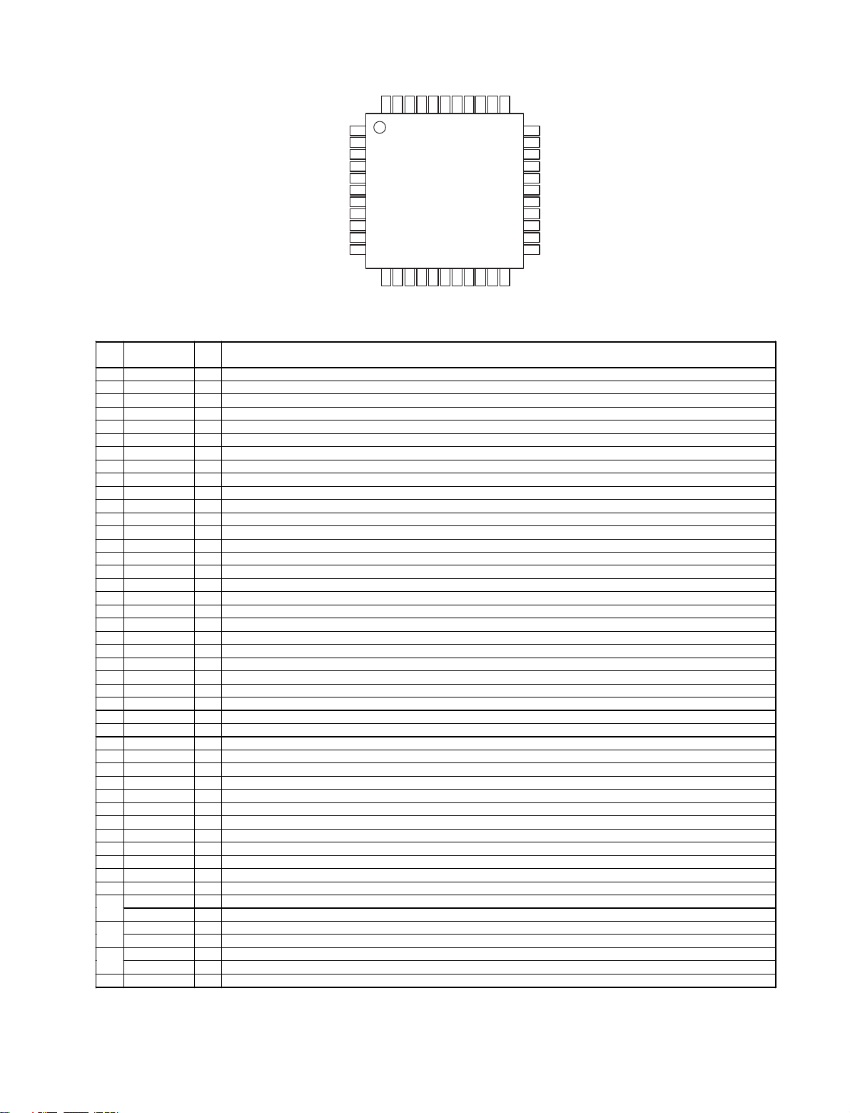
TMP93CS40F (AU: IC301)
7 5
7 6
1 0 0
1
5 1
5 0
2 6
2 5
TMP93CS40F Terminal Function
Pin
Name
No.
1 V REFL ⎯⎯⎯⎯⎯⎯A/D ref. GND
2 A Vss ← ⎯⎯⎯⎯⎯⎯A/D GND
3 A Vcc ← ⎯⎯⎯⎯⎯⎯AD +5V
4 _NMI I ⎯⎯⎯⎯⎯Not used (fixed to H)
5 P70/TI0 C15 O C Ed ⎯ L L Fixed to L (DSP ROM address cont. out bit 15, not used)
6 P71/TO1 C16 O C Ed ⎯ L L DSP program ROM address cont. out bit 16
7 P72/TO2 C17 O C Ed ⎯ L L DSP program ROM address cont. out bit 17
8 P73/TO3 ROM/RAM O C Ed ⎯ L L ROM/RAM switching control terminal (L:ROM)
9 P80/INT4/TI4 _INTREQ OUT I/O C Eu E↓&L Z ⎯ DSP request input and cont. output (L:Rq & cont.)
10 P81/INT5/TI5 B.DOWN I ⎯ Eu E↑&L Z ⎯ Power down detect (H: Detected)
11 P82/TO4 O C ⎯⎯ LL
12 P83/TO5 _REQ O C Eu ⎯ HL
13 P84/INT6/TI6 _ACK I ⎯ Eu E↓&L ⎯⎯MAIN-SUB CPU comm. control input (L: Ack. return from main)
14 P85/INT7/TI7 ERR I ⎯⎯E↑&L ⎯⎯DIR control input terminal (LC89055Q)( H: ERR)
15 P86/TO6 I ⎯⎯Lv Z ⎯ (GND)
16 P97/INT0 _CS I ⎯ Ed E↑&L ⎯⎯
17 P90/TXD0 S I O C MAIN-SUB CPU comm. control terminal (data output)
18 P91/RXD0 SO I ⎯ MAIN-SUB CPU comm. control terminal (data input)
19
P92/_CTS0/SCLK0
20 P93/TXD1 O C ⎯⎯ ZL
21 P94/RXD1 O C ⎯⎯ ZL
22 P95/SCLK1 O C ⎯⎯ ZL
23 AM8/_16 ← ⎯⎯⎯⎯⎯⎯Fixed to +5V
24 CLK O C Eu ⎯⎯⎯
25 Vcc ← ⎯⎯⎯⎯⎯⎯+5V
26 Vss I/O1 ⎯⎯⎯⎯⎯⎯GND
27 X1 Xin I ⎯⎯⎯⎯ ⎯X′tal connection
28 X2 Xout O ⎯⎯⎯⎯⎯X′tal connection
29 _EA ← ⎯⎯⎯⎯⎯⎯Fixed to +5V
30 _RESET RESET2_ I ⎯ Eu Lv L ⎯ Reset input (controlled by main CPU)
31 P96/XT1 A/D RESET O N Eu ⎯ H H A/D control terminal (L: Reset)
32 P97/XT2 O C Ed ⎯ LL
33 TEST1 ← I ⎯⎯⎯⎯⎯Connected to TEST2
34 TEST2 ← I ⎯⎯⎯⎯⎯Connected to TEST1
35 PA0 DINA O C Ed ⎯ L L Digital input switching control output
36 PA1 DINB O C Ed ⎯ L L Digital input switching control output
37 PA2 O C ⎯⎯ LL
38 PA3 DINC O C Ed ⎯ L L Digital input switching control output
39 PA4 DOUTA O C Ed ⎯ L L Digital output switching control output
40 PA5 DOUTB O C Ed ⎯ L L Digital output switching control output
Symbol
CLK I/O C MAIN-SUB CPU comm. control terminal (I2C clock in/output)
I/O Type Op Det Res Init
MAIN-SUB CPU comm. control output (L: Comm. request from
sub)
DIR control input terminal (LC89055Q), when CH status change
L→H
Function
Pin
Name
No.
41 PA6 DEEMP O C Ed ⎯ L L DAC de-emphasis filter cont. out terminal (H:ON)
42 PA7/SCOUT 96k-DAC O C ⎯⎯ L L DAC control terminal (H: Sample frequency 96kHz)
43 ALE O C ⎯⎯ L L (Address latch enable)
44 Vcc ⎯⎯⎯⎯⎯⎯+5V
45 P00/AD0 (AD0) I/O C ⎯⎯ Z L (EPROM data in D0 / address out A0)
46 P01/AD1 (AD1)) I/O C ⎯⎯ Z L (EPROM data in D1 / address out A1)
47 P02/AD2 (AD2) I/O C ⎯⎯ Z L (EPROM data in D2 / address out A2)
48 P03/AD3 (AD3) I/O C ⎯⎯ Z L (EPROM data in D3 / address out A3)
49 P04/AD4 (AD4) I/O C ⎯⎯ Z L (EPROM data in D4 / address out A4)
50 P05/AD5 (AD5) I/O C ⎯⎯ Z L (EPROM data in D5 / address out A5)
51 P06/AD6 (AD6) I/O C ⎯⎯ Z L (EPROM data in D6 / address out A6)
52 P07/AD7 (AD7) I/O C ⎯⎯ Z L (EPROM data in D7 / address out A7)
53 P10/AD8/A8 (A8) O C ⎯⎯ Z L (EPROM address out A8)
54 P11/AD9/A9 (A9) O C ⎯⎯ Z L (EPROM address out A9)
55 P12/AD10/A10 (A10) O C ⎯⎯ Z L (EPROM address out A10)
56 P13/AD11/A11 (A11) O C ⎯⎯ Z L (EPROM address out A11)
57 P14/AD12/A12 (A12) O C ⎯⎯ Z L (EPROM address out A12)
58 P15/AD13/A13 (A13) O C ⎯⎯ Z L (EPROM address out A13)
59 P16/AD14/A14 (A14) O C ⎯⎯ Z L (EPROM address out A14)
60 P17/AD15/A15 (A15) O C ⎯⎯ Z L (EPROM address out A15)
61 _WDTOUT ← OC⎯⎯Z H Watch dog output
62 Vss ← ⎯⎯⎯⎯⎯⎯GND
63 Vcc ← ⎯⎯⎯⎯⎯⎯+5V
64 P20/A0/A16 (A16) O C ⎯⎯ Z L (EPROM address out A16)
65 P21/A1/A17 DIR CLK O C ⎯⎯ Z L DIR control terminal (LC89055Q) control clock output
66 P22/A2/A18 DIR CE O C ⎯⎯ Z L DIR control terminal (LC89055Q) control chip enable output
67 P23/A3/A19 DIR MOSI O C ⎯⎯ Z L DIR control terminal (LC89055Q) control data output
68 P24/A4/A20 DIR MOSO I ⎯⎯Lv ⎯⎯DIR control terminal (LC89055Q) control data input
69 P25/A5/A21 FGAIN O C Ed ⎯ L L FRONT ch GAIN switching control output (H: SW=NO)
70 P26/A6/A22 DAC-RESET O C Ed ⎯ LH
71 P27/A7/A23 SEL CK O C ⎯⎯ Z L ADC/DIR data clock switching control terminal (L: ADC)
72 P30/_RD (_RD) O C ⎯⎯ Z L (Flash memory control terminal)
73 P31/_WR (_WR) O C ⎯⎯ Z L (Flash memory control terminal)
74 P32/_HWR CSI I ⎯⎯Lv ⎯⎯DIR control input terminal (L: PCM)
75 P33/_WAIT ERR MUTE_ O C Ed ⎯ L L Pop noise preventive mute control output (L: Mute)
76 P34/_BUSRQ I ⎯⎯Lv Z ⎯ GND
77 P35/_BUSRQ DIG.(AC3) MUTE O C Ed ⎯ Z L Digital mute control output (L: AC-3 or DTS decode enable)
78 P36/_R/W I ⎯⎯Lv Z ⎯ GND
79 P37/_RAS DIR RESET O C ⎯⎯ Z L DIR control output (LC89055Q) (L: Reset)
80
P40/_CS0/_CAS0
81
P41/_CS1/_CAS1
82
P42/_CS2/_CAS2
83 P60/PG00 DSP. RESET O C ⎯⎯ Z L DSP reset output terminal (L:Reset)
84 P61/PG01 I/02 SCD OUT I C ⎯ Lv Z ⎯ DSP status data input terminal
85 P62/PG02 I/03 DSP. CS O ⎯⎯⎯ Z L DSP chip select cont.output (L:Data out)
86 P63/PG03 I/04 DSP. CLK O C ⎯⎯ Z L DSP data clock output terminal
87 P64/PG10 I/05 SCD IN O C ⎯⎯ Z L DSP data output terminal
88 P65/PG11 I/06 4527_CE O C ⎯⎯ Z L AD control terminal (AK4527), Chip enable output
89 P66/PG12 I/07 4527_CLK O C ⎯⎯ Z L AD control terminal (AK4527), Data clock output
90 P67/PG13 I/08 4527_DIN O C ⎯⎯ Z L AD control terminal (AK4527), Data output
91 Vss ← ⎯⎯⎯⎯⎯⎯GND
92 P50/AN0 INTTREQ IN I ⎯ Eu Lv Z ⎯
93 P51/AN1 I ⎯ Eu Lv Z ⎯
94 P52/AN2 EMP I ⎯⎯Lv ⎯⎯H: EMP on
95 P53/AN3 96K DET I ⎯⎯Lv ⎯⎯96k signal detect input, H: 96k
96 P54/AN4 I ⎯ Eu Lv ⎯ Z
97 P55/AN5 I ⎯ Eu Lv ⎯ Z
98 P56/AN6 ACC ON/OFF I ⎯ Eu Lv ⎯ Z
99 P57/AN7 I ⎯ Eu Lv ⎯ Z
100 V REFH ← ⎯⎯⎯⎯⎯⎯AD ref. +5V
Symbol
(_CS0) O C ⎯⎯ Z L (Flash memory control terminal)
I/O Type Op Det Res Init
OC⎯⎯ZL
OC⎯⎯ZL
DAC control terminal (L: Power down mode, ↑(rising edge) Reset)
Function
16
Page 18
CS493292-CL (AU: IC814)
A0, SCCLK 7
DATA7, EMAD7, GPIO7 8
DATA6, EMAD6, GPIO6 9
DATA5, EMAD5, GPIO5 10
DATA4, EMAD4, GPIO4 11
VD2 12
DGND2 13
DATA3, EMAD3, GPIO3 14
DATA2, EMAD2, GPIO2 15
DATA1, EMAD1, GPIO1 16
DATA0, EMAD0, GPIO0
A1, SCDIN
RD, R/W, EMOE, GPIO11
WR/DS/EMWR, GPIO10
AUDATA3, XMT958
6
5
4
3
DGND1
2
Top View
VD1
1
MCLK
44
SCLK
43
LRCLK
42
AU DATA 0
AU DATA 1
41
40
AU DATA 2
39
DC
38
37
DD
36
RESET
35
AGND
34
VA
33
FILT1
32
FILT2
31
CLKSEL
30
CLKIN
29
CMPREQ, LRCLKN217
CS493292-CL Terminal Funtion
CS 18
SCDIO, SCDOUT,PSEL, GPIO9 19
VD3 23
DGND3 24
SDATAN1 22
ABOOT, INTREQ 20
EXTMEM, GPIO8 21
LRCLKN1 26
CMPCLK, SCLKN2 28
SCLKN1, STCCLK2 25
CMPDAT,SDATAN2, RCV958 27
Port Name FunctionPin No.
1,12,23 VD1,2,3 Digital power supply (+)
2,13,24 DGND1,2,3 Digital GND
3 AUDATA3, XMT958 SPDIF transmitter output, Digital audio output 3
4 WR, DS, EMWR, GPIO10
5 RD, R/W, EMOE,GPIO11
Host write strobe, Host data strobe, External memory write enable,
General purpose in/output 10
Host parallel output enable, Host parallel R/W, External memory write enable,
General purpose in/output 11
6 A1,SCDIN Host address bit 1, SPI serial control data input
7 A0,SCCLK Host address bit 0, Serial control port clock
8 DATA7, EMAD7, GPIO7 Bidirectional data bus 7, External memory address 7, General purpose in/output 7
9 DATA6, EMAD6, GPIO6 Bidirectional data bus 6, External memory address 6, General purpose in/output 6
10 DATA5, EMAD5, GPIO5 Bidirectional data bus 5, External memory address 5, General purpose in/output 5
11 DATA4, EMAD4, GPIO4 Bidirectional data bus 4, External memory address 4, General purpose in/output 4
14 DATA3, EMAD3, GPIO3 Bidirectional data bus 3, External memory address 3, General purpose in/output 3
15 DATA2, EMAD2, GPIO2 Bidirectional data bus 2, External memory address 2, General purpose in/output 2
16 DATA1, EMAD1, GPIO1 Bidirectional data bus 1, External memory address 1, General purpose in/output 1
17 DATA0, EMAD0, GPIO0 Bidirectional data bus 0, External memory address 0, General purpose in/output 0
18 CS Host parallel chip select, Host serial SPI chip select
19 SCDIO, SCDOUT, PSEL,GPIO9 Serial control port data in/output, Parallel port type select, General purpose in/output 9
20 INTREQ, ABOOT Control port interrupt request, Automatic boot enable
21 EXTMEM, GPIO8 External memory chip select, General purpose in/output 8
22 SDATAN1 PCM audio data input 1
25 SCLKN1, STCCLK2 PCM audio input bit clock
26 LRCLKN1 PCM audio input sample rate clock
27 CMPDAT, SDATAN2 PCM audio data input 2
28 CMPCLK, SCLKN2 PCM audio input bit clock
29 CMPREQ, LRCLKN2 PCM audio input sample rate clock
30 CLKIN Master clock input
31 CLKSEL DSP clock select
32 FILT2 PLL filter
33 FILT1 PLL filter
34 VA Analog power supply (+)
35 AGND Analog GND
36 RESET Master reset input
37 DD Reserved
38 DC Reserved
39 AUDATA2 Digital audio output 2
40 AUDATA1 Digital audio output 1
41 AUDATA0 Digital audio output 0
42 LRCLK Audio output sample rate clock
43 SCLK Audio output bit clock
44 MCLK Audio master clock
17
Page 19
LC89055W (AU: IC800)
D I
D O
E R R O R
B P S Y N C
A U T O
D G N D
D V D D
V F / P 3 / C 3
F 2 / P 2 / C 2
F 1 / P 1 / C 1
F 0 / P 0 / C 0
C S F L A G
A U D I O
E M P H A
X I N
X O U T
X M C K
D V D D
D G N D
X S T A T E
D A T A 0
L R C K
B C K
C K O U T
A V D D
A G N D
X S E L
M O D E 0
M O D E 1
D G N D
D V D D
D O S E L 0
D O S E L 1
C K S E L 0
C K S E L
X M O D E
C E
C L
1
R
V I N
D I N 0
D I N 1
D I N 2
D O U T
D I S E L
D G N D
L P F
D V D D
LC89055W Terminal Function
Pin
No.
Pin Name
I/O
1 DISEL I Data input terminal (select input pin of DIN0, DIN1)
2 DOUT O Input bi-phase data through output terminal
3 DIN0 I Amp built-in coaxial/optical input correspond data input terminal
4 DIN1 I Amp built-in coaxial/optical input correspond data input terminal
5 DIN2 I Optical input correspond data input terminal
6 DGND Digital GND
7 DVDD Digital power supply
8 R I VCO gain control input terminal
9 VIN I VCO free-run frequency setting input terminal
10 LPF O PLL loop filter setting terminal
11 AVDD Analog power supply
12 AGND Analog GND
13 CKOUT O Clock output terminal (256fs, 384fs, 512fs, X′tal osc., VCO free-run osc.)
14 BCK O 64fs clock output terminal
15 LRCK O fs clock output terminal (L: Rch, H: Lch, I2S: Reverse)
16 DATAO O Data o utput te rmi na l
17 XSTATE O Input data detecting result output terminal
18 DGND Digital GND
19 DVDD Digital power supply
20 XMCK O X′tal osc. clock output terminal (24.576MHz or 12.288MHz)
21 XOUT O X′tal osc. connection output terminal
22 XIN I X′tal osc. connection input terminal, external signal input possible (24.576MHz or 12.288MHz)
23 EMPHA O Emphasis information output terminal of channel status
24 AUDIO O Bit1 output terminal of channel status
25 CSFLAG O Top 40bit revise flag output terminal of channel status
26 F0/P0/C0 O Input fs cal. sig. out / data type out / input word inf. output terminal
27 F1/P1/C1 O Input fs cal. sig. out / data type out / input word inf. output terminal
28 F2/P2/C2 O Input fs cal. sig. out / data type out / input word inf. output terminal
29 VF/P3/C3 O Validity flag out / data type out / input word inf. output terminal
30 DVDD Digital power supply
31 DGND Digital GND
32 AUTO O Non PCM burst data transfer detect sig. output terminal
33 BPSYNC O Non PCM burst data preamble Pa, Pb, Pc, Pd sync sig. output terminal
34 ERROR O PLL lock error, data error flag output terminal
35 DO O CPU I/F read data output terminal
36 DI I CPU I/F write data input terminal
37 CE I CPU I/F chip enable input terminal
38 CL I CPU I/F clock input terminal
39 XSEL I Frequency select input pin of XIN X′tal osc. (24.576MHz or 12.288MHz)
40 MODE0 I Mode setting input terminal
41 MODE1 I Mode setting input terminal
42 DGND Digital GND
43 DVDD Digital power supply
44 DOSEL0 I Data output format select input terminal
45 DOSEL1 I Data output format select input terminal
46 CKSEL0 I Output clock select input terminal
47 CKSEL1 I Output clock select input terminal
48 XMODE I Reset input terminal
* For latch-up countermeasure, set digital (DVDD) and analog (AVDD) power on/off in the same timing.
Function
18
Page 20
M35015-210SP (AU: IC453)
O S C 1
O S C 2
C V I D E O
L E C H A
C V I N
1
2
3
C S
4
S C K
S I N
5
6
A C
V
D D 2
7
8
9
1 0
2 0
V
D D 1
1 9
V E R T *
1 8
H O R *
1 7
O S C I N
1 6
O S C O U T
1 5
P 3
1 4
P 2
1 3
P 1
1 2
P 0
1 1
V s s
C S
S C K
S I N
S Y N C S I G N A L
H O R *V E R T *O S C 2O S C 1
S Y N C S I G N A L D I S -
C R I M I N A T I N G C I R C U I T
O S C C I R C U I T
F O R S Y N C S I G N A L
G E N E R A T I O N
T I M I N G
G E N E R A T O R
1 7
1 6
O S C I N
O S C O U T
1 2 1 9 1 8
3
I N P U T
4
C O N T R O L
C I R C U I T
5
U I T
I N D I C A T I O N
C O N T R O L
R E G I S T E R
A D D R E S S
C O N T R O L
C I R C U I T
D A T A
C O N T R O L
C I R C
I N D I C A T I O N
O S C I L L A T O R
T I M I N G
G E N E R A T O R
I I N D I C A T I O N L O C A T I O N
D E T E C T I O N C I R C U I T
R E A D O U T A D D R E S S
C O N T R O L C I R C U I T
S W I T C H I N G C I R C U I T
H C O U N T E R
V
D D 1
2 0
6
A C
1 1
V s s
7
V
D D 2
I N D I C A T I O N R A M
I N D I C A T I O N C H A R A C T E R R O
M
B L I N K I N G C I R C U I T
I N D I C A T I O N
C O N T R O L C I R C U I T
S H I F T R E G I S T E R
N T S C
V I D E O O U T P U T
C I R C U I T
M35015-210SP Terminal Function
Pin No. Symbol Name I/O Function
1 OSC1 Osc. circuit ext. I External terminal for indication oscillator circuit. Standard OSC. freq. is approx. 7MHz.
2 OSC2 terminal. O With this OSC. freq., decides horizontal indicatin and character width.
3 CS Chip select input I
4 SCK Serial clock input I
5 SIN Serial data input I
6 AC Auto-clear input I
DD2
7V
8CVIDEO
9 LECHA
10 CVIN
Power supply
Combined
video output
Character level
input
Combined video
input
11 Vss Ground
12 P0 Output port p0 O
13 P1 Output port P1 O
14 P2 Output port P2 O
15 P3 Output port P3 O
16 OSCOUT O Terminal for external use of sync signal OSC. circuit. Use the freq.: 14.32MHz at NTSC
17 OSCIN I system, 17.73MHz at PAL. system, 14.30MHz at MPAL system.
18 HOR*
19 VERT*
DD1
20 V
Ext. terminal
for sync sig.
OSC. Circuit
Horizontal sync
signal
Vertical sync
signal
Power supply I Power supply terminal of digital system. Connect to +5V.
Chip select terminal and turns to “L” when transfer serial data.
Hysteresis input. Pull up resistor is built-in.
Takes in serial data of SIN at SCK rise when CS terminal is in “L”.
Hysteresis input. Pull up rersist is built-in.
Serial input of register for indication control and data, and address for indication data
memory. Hysteresis input. Pull up rersistor is built-in.
Resets internal circuit of IC at “L” mode.
Hysteresi input. Pull up resistor is built-in.
Power supply terminal of analog system. Connect to +5V.
Output terminal of combined video signal. Outputs 2Vp-p combined signal. Character
O
output, etc. Overlap CVIN signal and outputs at superimpose.
Input terminal deciding character output level in combined video signal. color of character
I
is white.
Input terminal of external combined video signal.
I
Character output etc. overlap this external combined video signal.
Ground terminal. Connect to GND.
General output or character background signal BL NK1* output is switchable.
Polarity can be selected at ROM mask.
General output or character background signal CO1* output is switchable.
Polarity can be selected at ROM mask.
General output or character background signal BLNK2* output is switchable.
Polarity can be selected at ROM mask.
General output or character background signal CO2* output is switchable.
Polarity can be selected at ROM mask.
Inputs horizontal sync signal.
I
Hysteresis input.
Input vertical sync signal. Hysteresis input. Polarity can be selected at ROM mask.
8
C V I D E O
9
L E C H A
1 0
C V I N
P 0
1 2
1 3
P 1
1 4
P 2
1 5
P 3
19
Page 21
AK4527BVQ (AU:IC602)
SDOS
I2C
SMUTE
BICK
LRCK
SDTI1
SDTI2
SDTI3
SDTO
DAUX
DFS
L0OP1
L0OP0/SDA/CDTI
DIF0/CSL
P/S
MCLK
DIF1/SCL/CCLK
39
13 14
DEM1
DEM0
41
15
TVDD
40
Top View
16 17 18
DVDD
DVSS
PDN
444342
1
2
3
4
5
6
7
8
9
10
11
12
38
ICKS2
DZF1
AVSS
37
192021
ICKS1
36
AVDD
35
ICKS0
VREFH
VCOM
34
22
CAD1
CAD0
33
DZF2
32
RIN+
31
RIN–
30
LIN+
29
LIN–
28
ROUT1
27
LOUT1
26
ROUT2
25
LOUT2
24
ROUT3
23
LOUT3
AK4527BVQ Terminal Function
Pin
Pin Name I/O Function
No.
1 SDOS I SDTO source select pin, L: Internal ADC output, H: DAUX input
2 I2C I Serial control mode select pin, L: 3-core serial, H: I2C bus
3 SMUTE I Soft mute pin, H: Soft mute start, L: Release
4 BICK I Audio serial data clock pin
5 LRCK I Input channel clock pin
6 SDTI1 I DAC1 audio serial data input pin
7 SDTI2 I DAC2 audio serial data input pin
8 SDTI3 I DAC3 audio serial data input pin
9 SDTO O Audio serial data output pin
10 DAUX I Auxiliary audio serial data input pin
11 DFS I Double speed sampling mode pin, L: Normal, H: Double
12 NC No Connect, No internal bonding
13 DZFE I Zero input detect enable pin
14 TVDD Power pin for output buffer, 2.7V~5.5V
15 DVDD Digital power pin, 4.5V~5.5V
16 DVss Digital GND pin, 0V
17 PDN I Power down & reset pin, L: Powered-down and register initialized, Reset with PDN when switching CAD0-1
18 TST I Test pin, connected to DVSS
19 NC No Connect, No internal bonding
20 ADIF I Analog Input Format Select pin
21 CAD1 I Chip address-1 pin
22 CAD0 I Chip address-0 pin
23 LOUT3 O DAC3L channel analog out pin
24 ROUT3 O DAC3R channel analog out pin
25 LOUT2 O DAC2L channel analog out pin
26 ROUT2 O DAC2R channel analog out pin
27 LOUT1 O DAC1L channel analog out pin
28 ROUT1 O DAC1R channel analog out pin
29 LIN- I L-ch analog inverted input pin
30 LIN+ I L-ch analog non-inverted input pin
31 RIN- I R-ch analog inverted input pin
32 RIN+ I R-ch analog non-inverted input pin
33 DZF2/OVF O 0 input detect 2 pin/Analog input overflow detect pin
34 VCOM O Common V-out pin, AVDD/2, connect large capacitor to avoid noise
35 VREFH I Ref. V input pin, AVDD
36 AVDD Analog GND pin, 4.5V~5.5V
37 AVss Analog GND pin, 0V
38 DZF1 O 0 input detect pin, H: Input data of G1 is 8192 times “0” in a raw or RSTN bit “0”, L: When P/S= “0”
39 MCLK I Master clock input pin
40 P/S I Parallel/Serial select pin, L: Serial control
DIF0 I Audio data I/F format 0 pin (parallel control)
41
CSN I Chip select pin (3-wire serial control), connect to DVDD when I
DIFI I Audio data I/F format 1 pin (parallel control)
42
SCL/CCLK I Control data clock pin (serial control), I
LOOP0 I Loop back mode 0 pin (parallel control), effects digital loop back ADC to all DAC
43
SDA/CDTI I/O Control data input pin (serial control), I
2
C=”L”: CCLK (3-wire serial), I2C=”H”: SCL (I2C bus)
2
C=”L”: CCTI (3-wire serial), I2C=”H” SDA (I2C bus)
44 LOOP1 I Loop back mode 1 pin, from SDT1 to all DAC
2
C bus control
20
Page 22
BU4094BCF (CO: IC304,305)
STROBE
DATA
CLOCK
V
1
2
3
4
Q1
5
Q2
6
Q3
7
Q4
8
SS
16
VDD
15
OE
14
Q5
13
Q6
12
Q7
Q8
11
10
Q'
S
Q
S
9
CO: IC304
Port
Q1 A Video input switching
Q2 B Video input switching
Q3 C Video input switching
Q4 D Video output switching
Q5 E Video output switching
Q6 F Video output switching
Q7 H Video output switching
Q8 G Video output switching
Symbol Function
CO: IC305
Port
Q1
Q2 S1 Video signal switching control output
Q3 S2 Video signal switching control output
Q4 EXT. IN
Q5 D Video output switching
Q6 G Video output switching
Q7 NC
Q8 FRONT A+B Current limiter control terminal (H:Front SP A+B)
Symbol Function
DIRECT/TONE DEFEAT
DIRECT & TONE DEFEAT relay control (H:DIRECT,TONE DEFEAT)
Sub woofer channel gain control terminal (L:EXT. IN)
LC75721E (CO: IC101)
G7 G8G9
G10
G11
AA8/G12
AA7/G13
AA6/G14
AA5/G15
AA4/G16
48 33
49
DI
CL
CE
RES
DD
V
OSCI
OSCO
Vss
TEST
FL
V
G1
G2
G3
G4
G5
G6
64
AM 1
AM 2
AM 3
AM 4
AM 5
AM 6
AM 7
AM 8
AM 9
AM 10
AA3
AM 11
AA2
AM 12
AA1
AM 13
AM35
AM 14
AM34
AM 15
AM33
161
AM 16
32
17
LC75721E Terminal Function
Symbol
V
DD
Vss
FL
V
AM 17
AM 18
DI
AM 19
AM 20
CL
AM 21
CE
AM 22
AM 23
AM 24
OSCI
AM 25
OSCO
AM 26
AM 27
RES
AM 28
AM 29
AM1~AM35
AM 30
AA1~AA3
AM 31
AM 32
AA4/G16
AA5/G15
AA6/G14
AA7/G13
AA8/G12
G1~G11 Grid output terminal
TEST LSI test terminal
Function
Power terminal +5V
Power terminal GND
Power terminal FL drive
Serial data transfer terminal
DI: Data
CL: Clock
CE: Chip enable
External CR connecting terminal
System reset terminal
Anode output terminal
Anode/Grid output terminal
BU2090F (CO: IC103)
1Vss
2DATA
3CLOCK
4LCK
5Q0
6Q1
7Q2
8Q3
9Q4
TC9274N-011 (AU: IC107) TC9274N-017 (EX: IC312)
S1S2S3S4S5S6S7S8S9
41
40
V
DD
42
36
3839
37
S10
35
18 bit Latch Circuit (Rch)
(Lch) Same as Rch
S11
32
34
33
S12
S13
S14
S15
S16
S17
S18
26
29
28
3031
24
25
27
23
STB
22
DATA
S1S2S3S4S5S6S7S8S9
41
40
V
DD
42
36
3839
37
S10
35
18 bit Latch Circuit (Rch)
(Lch) Same as Rch
S11
32
34
33
CONTROL CIRCUIT
12-bit SHIFT RESISTER
12-bit STRAGE RESISTER
OUTPUT BUFFER (OPEN DRAIN)
S12
S13
S14
S15
S16
26
29
28
27
3031
DD
18
V
OE
17
Q11
16
Q10
15
Q9
14
Q8
13
Q7
12
Q6
11
Q5
10
S17
S18
24
25
23
STB
22
DATA
V
SS
1
2
345678 9 10 111213 14
S1S2S3S4S5S6S7S8S9
21
CK
Level Shift + Shift Register Circuit
20
GND
16 171819
15
S10
S11
S12
S13
S14
S15
S16
S17
S18
V
SS
1
2
34567891011
S1S2S3S4S5S6S7S8S9
12
S10
16 171819
14
15
13
S11
S12
S13
S14
S15
S16
S17
21
CK
Level Shift + Shift Register Circuit
20
GND
S18
21
Page 23
TC9273N-004 (AU: IC108)
Vss
1
S1
2
S2
3
4
S3
S4
5
6
S5
7
S6
S7
8
9
S8
10
S9
11
S10
12
V
DD
28
S1
27
S2
26
25
S3
S4
24
23
S5
22
S6
S7
21
20
S8
19
S9
18
S10
17
TC9273N Terminal Function
Symbol Name
Pin No
1
13
28
2~12
12~27
14
15
16
Vss
GND
V
DD
S1~S10
CK
DATA
STB
+Power Terminal
Digital Ground
+Power Terminal
I/O Terminal
Clock Input
Data Input
Dual Power Use:VDD = 8.0~17 V Single Power Use:VDD = 8.0~18V
Input terminal of analog switch.
Clock input for data transfer.
Serial input for switch setting.
Strobe InputStrobe input for data writing.Strobe Input
Function
GND=0V
Vss=-8.0~-17V
GND=0V
Low level
Border Input
Terminal
13
GND
14
CK
STB
DATA
16
15
NJM2229S (AU: IC452)
AD1854 (AU: IC601)
1
DGND
2
MCLK
3
CLATCH
4
CCLK
5
CDATA
6
384/256
7
X2MCLK
8
ZEROR
9
DEEMP
10
96/48
11
AGND
12
OUTR+
13
OUTR−
14
FILTR
28
27
26
25
24
23
22
21
20
19
18
17
16
15
1
DVDD
SDATA
BCLK
L/RCLK
PD/RST
MUTE
ZEROL
IDPM0
IDPM1
FILTB
AVDD
OUTL+
OUTL−
AGND
7
15
6
Sync Sepa
Vsync Sepa
FRONT VIEW
16
14
13
Sync Det
11
12
8
Phase
Det
4
32fH
VCO
3
2
Terminal Function
No.
11,15 AGND I Analog Ground
Name Function
I/O
1 DGND I Digital Ground.
2 MCLK I Master Clock Input
3 CLATCH I Latch input for control data
4 CCLK I Control clock input for control data
5 CDATA I Serial control input
6 384/256 I Selects the master clock mode
7 X2MCLK I Selects internal clock doubler (LO) or internal clock=MCLK (HI)
8 ZEROR O Right Channel Zero Flag Output
9 DEEMP I De-Emphasis
10 96/48 I Selects 48kHz (LO) or 96kHz Sample Frequency Control
12 OUTR+ O Right Channel Positive line level analog output
13 OUTR- O Right Channel Negative line level analog output
14 FILTR O Voltage Reference Filter Capacitor Connection
16 OUTL- O Left Channel Negative line level analog output
17 OUTL+ O Left Channel Positive line level analog output
18 AVDD I Analog Power supply
19 FILTB O Filter Capacitor connection
20 IDPM1 I Input serial data port mode control one
21 IDPM0 I Input serial data port mode control zero
22 ZEROL O Left Channel Zero Flag output
23 MUTE I Mute. Assert HI to mute both stereo analog output
24 PD/RST I Power-Down/Reset
25 L/R CLK I Left/Right clock input for input data
26 BCLK I Bit clock input for input data
27 SDATA I Serial input
28 DVDD I Digital Power Supply
9
1
10
1/32
5
16
22
Page 24
SN74LV244APW (AU: IC818, 825)
1OE
1A1
2Y4
1A2
2Y3
1A3
2Y2
1A4
2Y1
GND
1
2
3
4
5
6
7
8
9
10
TOP VIEW
Vcc
20
2OE
19
1Y1
18
2A4
17
1Y2
16
2A3
15
1Y3
14
2A2
13
12
1Y4
11
2A1
FUNCTION TABLE
(each buffer)
INPUT
OE A Y
LH H
LL L
HX Z
OUTPUT
BU4053BCF (AU:IC256)
MM74HC4053SJ (AU: IC451)
Z-COM
INH
V
Vss
Y1
Y0
Z1
Z0
EE
TOP VIEW
1
2
3
4
5
6
7
8
$
#
"
!
12
11
9
DD
V
Y-COM
X-COM
X1
X0
A
B
C
V
INH6
Vss8
V
X0 12
X1 13
Y0 2
Y1 1
Z0 5
Z1 3
DD
A11
B10
16
C9
EE
7
LEVEL
CONVER
-TER
BINARY TO 1 of 2
DECODER WITH INHIBIT
14 X
15 Y
4 Z
TC9459N
(EX: IC805)
TOP VIEW TOP VIEW
Vss
L-OUT
L-IN
L-LD1
L-LD2
L-A-GND
CS1
GND
1
2
NC
3
4
NC
5
6
7
8
9
NC
10
NC
11
NC
12
13
14
CK
28
27
26
25
24
23
22
21
20
19
18
17
16
15
TC9184AP (EX: IC102)
TOP VIEW
Vss
BASS+
BASS-
COM
TREBLE-
TREBLE+
GND
CK
1
2
3
4
5
5
6
7
8
16
15
14
13
12
11
10
9
V
DD
NC
R-OUT
NC
R-IN
R-LD1
R-LD2
R-A-GND
NC
CS2
NC
NC
STB
DATA
V
DD
BASS+
BASS-
COM
TREBLE-
TREBLE+
STB
DATA
L-OUT
NC
L-IN
L-LD1
L-LD2
L-A-GND
CS1
GND
NC
NC
NC
NC
CK
BASS+
BASS-
TC9482N
(EX: IC809)
SS
V
1
2
3
Ω
/
50k
TEP
91S
4
VR
5
6
7
8
9
L-ch7 to 91decoder
L-ch latch circuit
10
11
12
13
14
Shift register (24Bit)
Level shift circuit
VSS
1
2
3
Ladder resister
DD
V
28
Same
R-ch7 to 91decoder
R-ch latch circuit
VDD
16
Analog switch
as L-ch
GND
7
13 bit latch circuit
27
26
25
24
23
22
21
20
19
18
17
16
15
NC
R-OUT
NC
R-IN
R-LD1
R-LD2
R-A-GND
NC
CS2
NC
NC
STB
DATA
DATA
CK
9
8
Level shift
L-OUTA
L-INA
L-A-GNDA
L-OUTB
L-INB
L-A-GNDB
L-OUTC
L-INC
L-A-GNDC
GND
STB
10
Vss
NC
CS1
CK
1
2
3
4
5
6
7
8
9
10
11
12
13
14
Analog switch
Ladder resister
28
27
26
25
24
23
22
21
20
19
18
17
16
15
15
14
V
DD
TEST
R-OUTA
R-INA
R-A-GNDA
R-OUTB
R-INB
R-A-GNDB
R-OUTC
R-INC
R-A-GNDC
CS2
STB
DATA
BASS+
BASS-
COM
TREBLE-
TREBLE+
4
5
13
12
COM
TREBLE-
20 bit Shift register circuit
Analog switch
6
Ladder resister
13 bit latch circuit
Code
detect
circuit
Analog switch
Ladder resister
11
TREBLE+
23
Page 25
BU4052BCF (AU:IC255,509,510)
AT49LV002T (AU:IC817)
TOP VIEW
Y
4
1
Y
0
X
2
Y
Y
2
2
2
Common
Y
3
Y
Y
3
4
5
Y
1
6
INH
7
EE
V
8
Vss
OUT/IN
Y
3
Y
1
INH
V
EE
OUT/IN
B
X
1
X
X
0
X
3
A
SN74AHC574PW
(AU: IC815, 816)
1
OE
2
1D
2D
3
4
3D
5
4D
5D
6
6D
7
8
7D
8D
9
10
GND
16
15
14
13
12
11
10
9
V
DD
X
2
X
1
Common
X
X
0
X
3
A
B
20
19
18
17
16
15
14
13
12
11
Vcc
1Q
2Q
3Q
4Q
5Q
6Q
7Q
8Q
CK
INH
L
L
L
L
H
X:Don't Care
FUNCTION TABLE
A B ON SWITCH
LLX
HL
LH
HH
XX
Y
00
XY
11
XY
22
XY
33
NONE
RESET
A16
A15
A12
A7
A6
A5
A4
A3
A2
A1
A0
I/O 0
I/O 1
I/O 2
GND
SN74HC151NS (EX:IC505,506)
logic symbol
1
CE
CLK
1D
2D
3D 3Q
4D
5D 5Q
6D 6Q
7D
8D 8Q
EN
11
C1
2
1D
3
417
5
615
714
8
912
19
1Q
18
2Q
16
13
Outputs
4Q
7Q
1
2
3
4
5
6
7
8
9
10
11
12
13
14
15
16
Data
Inputs
Strobe
TOP VIEW
3
1
2
2
1
3
0
4
5
5
Y
W
6
7
GND
8
D2
D1
D0
Y
W
S
FUNCTION TABLE
C
VCC
WE
A17
A14
A13
A8
A9
A11
OE
A10
CE
I/O 7
I/O 6
I/O 5
I/O 4
I/O 3
D4
D5
D6
D7
A
B
Pin Name
A0 - A17
CE
OE
WE
RESET
I/O0 -I/O7
DC
16
Vcc
4
15
5
14
6
13
12
7
A
11
B
10
C
9
Data
Inputs
Data
Select
32
31
30
29
28
27
26
25
24
23
22
21
20
19
18
17
Function
Addresses
Chip Enable
Output Enable
Write Enable
RESET
Data Inputs/Outputs
Don't Connect
BU4051BCF
(AU:IC251,252,504~507)
X
Channel
Common
OUT/IN
INHIBIT
4
1
X
6
IN/OUT
X
X
7
X
5
V
EE
Vss
4
2
6
3
OUT/IN
4
7
5
5
6
INH
7
V
EE
C
8
V
DD
16
X
2
15
2
X
1
14
1
13
X
0
0
X
3
12
3
A
11
A
10
B
B
9
C
SN74LV00APW
(AU: IC807)
1
GND
1A
1B
2
1Y
3
2A
4
2B
5
6
2Y
7
Vcc
14
4B
13
4A
12
4Y
11
3B
10
9
3A
3Y
8
TC74VHC123AF
(AU: IC801)
1A
1
1B
2
1CLR
3
Channel
IN/OUT
1Q
4
5
5
2Q
2Cex1
6
GND
7
8
2Rext/Cext
SN74LV14APW
(AU: IC809)
1
1A
2
1Y
2A
3
4
2Y
5
3A
3Y
6
GND
7
QQ
CLR
QQ
CLR
74LVX157
(AU: IC804)
16
15
14
13
12
11
10
9
Vcc
1Rex/Cext
1Cext
1Q
2Q
2CLR
2B
2A
SE
LECT
GND
1
1A
2
3
1B
1Y
4
5
5
2A
2B
6
7
2Y
8
SEL
16
15
14
13
12
11
10
Vcc
ST
4A
4B
4Y
3A
3B
9
3Y
SN74LV4040APW
(AU: IC813)
OL
Outputs
OG
GND
1
OF
OE
OD
OC
OB
OL
2
OF
3
OE
4
OG
5
OD
6
OC
7
8
CLR
OB
CLK
OA
Vcc
14
13
6A
6Y
12
5A
11
5Y
10
9
4A
4Y
8
Vcc
16
OK
15
OK
OJ
14
OJ
13
OH
OH
OI
Outputs
OI
12
CLR
11
10
CLK
Outputs
9
OA
TC74HCU04AF
(EX:IC504)
1
1A
2
1Y
3
2A
4
2Y
5
3A
6
3Y
GND
7
TC74HCT7007AF
(AU:IC823)
1A
1
1Y
2
2A
3
2Y
4
3A
5
3Y
6
7
GND
14
Vcc
13
6A
6Y
12
11
5A
5Y
10
4A
9
8
4Y
14
Vcc
13
6A
6Y
12
11
5A
5Y
10
4A
9
8
4Y
24
Page 26
BA033T (AU: IC819)
)
KIA7805API (RE: IC901, 902, 907)
KIA7806API (PO: IC501)
KIA7812API (RE: IC905)
FRONT
VIEW
KIA7905PI (RE: IC909)
KIA7912PI (RE: IC906)
FRONT
VIEW
BA15218F (AU: IC112)
BA4510F (AU: IC811, 812)
NJM2068MD (EX: IC103, 301, 302,
308~310, 701, 801~804)
(AU: IC109, 701, 721, 741, 761
TK15420MTL (AU: IC253, 254, 257,
501~503, 508, 511)
GND
Input
Output
NJM2391DL1 (AU: IC824)
TOP VIEW
GND
IN OUT
OPTICAL
INPUT
GP1FA551RZ (EX:IC501~503)
FRONT VIEW
GND
Input
Output
LC72720NM (CO: IC105)
Europe Model Only
TOP VIEW
V
REF
1
MPXIN
2
3
V
dda
V
ssa
4
5
FLOUT
CIN
6
T1
7
T2
8
XOUT
9
10
11
12
T3(RDCL)
T4(RDDA)
T5(RSFT)
OUTPUT
GP1FA551TZ(EX:IC707)
FRONT VIEW
24
SYR
23
CE
DI
22
CL
21
DO
20
RDS-ID
19
SYNC
18
T7(OORREC/ARI-ID/BEO)
17
16
T6(ERROR/57K/BEI)
15
V
ssd
14
V
ddd
XIN
13
A OUTPUT
A –INPUT
A +INPUT
1
1
2
3
V
4
V
8
B OUTPUT
7
2
B –INPUT
6
B +INPUT
5
IC PROTECTOR
ICP-N15 (PO: IC502)
FRONT VIEW
Vcc
Vout
GND
OTHERS
GP1U27X (Remote Control Sensor)
(CO: IC102)
TOP VIEW
Head
Amp
Vcc
Vout
GND
V
CC
V
OUT
GND
Limiter
Amp
BPF
Vin
Vcc
GND
Detector &
Comparator
LED
Integrator
DRIVE
GND
IC
Hysteresis
Comparator
Vcc
Vout
V
CC
Vin
GND
25
Page 27
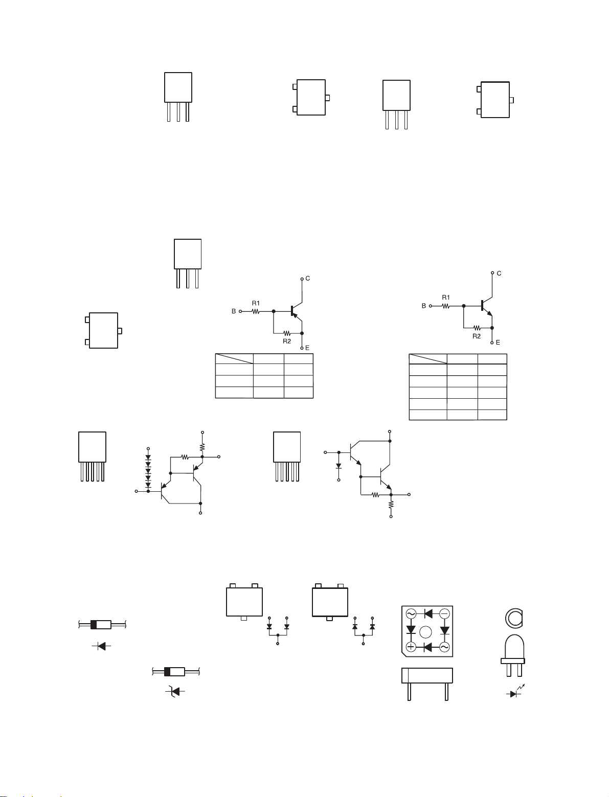
TRANSISTORS
B
2SA1505Y
2SC2412K (S)
2SD601A
KTC2875B
B
E
2SA970 (BL)
2SA988 (E/F)
2SA933S (S)
2SA1145 (O/Y)
2SC1740S (S)
2SC2705 (O/Y)
FRONT
VIEW
C
E
2SC3311A
2SD2144STPU
KTA1266 (GR)
KTC2874B
2SC/KTC3200(BL)
DTA114EK
DTC114ES
DTA114TK
DTA144EK
DTC114EK
FRONT
VIEW
DTC143EK
DTC144EK
DTC323TK
B
TOP
C
VIEW
E
MP15P MN15N
FRONT
VIEW
D
C
E
R:70W Typ.
B
E
DTA114TK
DTA114EK
DTA144EK
DTA114EK
DTA114TK
DTA144EK
RE:0.22W Typ.
S
PNP Type
R1
10kohm
10kohm
47kohm
FRONT
10kohm
47kohm
VIEW
R2
-
TOP
VIEW
2SB/KTB778 (R/O) 2SK771
C
FRONT
VIEW
BCE
S
TOP
G
VIEW
D
DTC114EK
DTC114ES
DTC143EK
DTC144EK
DTC323TK
C
B
NPN Type
R1
DTC114EK
DTC114ES
DTC143EK
DTC144EK
DTC323TK 2.2kohm
10kohm
10kohm
4.7kohm
47kohm
R2
10kohm
10kohm
4.7kohm
47kohm
-
ES CDB
DIODES (included LED)
1SR35-400A
1SS270A
RB721Q-40
B
HZS3C-2
HZS5C-1
HZS6A-1
HZS6A-2
HZS7B-2
HZS9B-1
HZS33-2
MTZJ18A
C
DAN202K
2
1
TOP
VIEW
3
1: Anode
2: Anode
3: Cathode
BDCSE
1
3
DAP202K
2
D
2
1
TOP
VIEW
3
1: Cathode
2: Cathode
3: Anode
R:70W Typ.
1
3
2
RE:0.22W Typ.
E
S4VB20
S4VB20F
S
TOP VIEW
SEL1210S (Red)
SEL1410E (Green)
TOP VIEW
26
Page 28
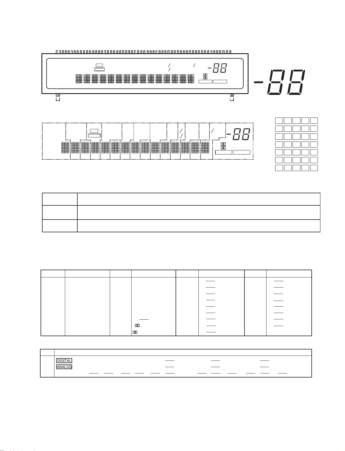
FL DISPLAY
CM1690C (CO: FL101)
1
STEREO
TUNED
RDS
CH
G16
TUNED
RDS
CH
G15
STEREO
AUTO
Pin Assignment
PIN NO.
CONNECTION
PIN NO.
CONNECTION
PIN NO.
CONNECTION
58
S15
S12
S10
S11
S9
G1
S5
S4
S6
S7
S1
S2
S3
AUTO
REC
MULTI
PHONO
VCR
CD
AUX
3
V.AUX
DVDMDVDP
TAPE
TUNER
−
1
−2−
TV
−
1
DBS
−
2
PRO LOGIC
DIGITAL
DIGITAL ANALOG
S38
S14
S13
F2F1
G2~G16
G12
G10
G13
REC
PHONO
MULTI
VCR
G14 G11 G8
CD
−
1
G9
TUNER
−2−
12345
F1 F1 S1 S2 S3
21 22
23 24 25
S4
26
G7
AUX
V.AUX
3
78910111213141516171819
6
G5 G2 G1
G6
DVD
MD
G4
VDP
TAPE
G3
TV
−
DBS
−
2
1
PRO LOGIC
DIGITAL
DIGITAL ANALOG
S1
S6
S11
S16
S21
S26
S31
S5 S6 S7 S8 S9 S10 S11 S12 S13 S14 S15
27 28 29 30 31 32 33 34
35 36 37 38 39 40
S7
S8
S12
S13
S18
S17
S22
S23
S28
S27
S32
S33
S16 S17
S9
S14
S19
S24
S29
S34
S5
S10
S15
S20
S25
S30
S35
20
S18
S4
S2
S3
S19 S20 S21 S22 S23 S24 S25 S26 S27 S28 S29 S30 S31 S32 S33 S34 S35 S36 S37 S38
41 42 43 44 45
47 48 49 50 51 52 53 54 55 56 57
46
58
G16 G15 G14 G13 G12 G11 G10 G9 G8 G7 G6 G5 G4 G3 G2 G1 F2 F2
F1,F2 : Filament
G1~G16 : Grid
S1~S38 : Anode
Anode & Grid Assignment
G1
G2~G16
S36
S37
S38
S1
S2
S3
S4
S5
S6
S7
S1
S2
S3
S4
S5
S6
S7
S8
S9
S9
G1 G2 G3 G4 G5 G6 G7 G8 G9 G10 G11 G12 G13 G14 G15
/
−2
S38
DBS
TV
−1
S1
S2
S3
S4
S5
S6
S7
S8
S9
VDP
TAPE
S10
S11
S12
S13
S14
S15
S16
S17
S18
/(DVD)
/(MD)
G1
S10
S11
S12
S13
S14
S15
DIGITAL
PRO LOGIC
DVD
MD
V.AUX
G2~G16
AUX
S10
S11
S12
S13
S14
S15
S16
S17
S18
S19
S20
S21
S22
S23
S24
S25
S26
S27
TUNER
−2
−3
CD
−1
G1
G2~G16
S19
S20
S21
S22
S23
S24
S25
S26
S27
PHONO
VCR
S28
S29
S30
S31
S32
S33
S34
S35
REC
MULTI
G1
STEREO
AUTO
G2~G16
S28
S29
S30
S31
S32
S33
S34
S35
G16
TUNED
RDS
CH
27
Page 29
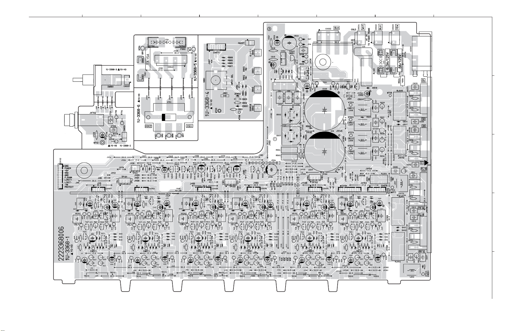
PRINTED WIRING BOARDS
1
1U-3368 POWER P.W.B. Ass'y
2
3
4
5
76
8
13
7
4
3
1
1
113
12
13
12
12
12
A
B
3
1
110
17191515151515
C
COMPONENT SIDE
D
E
28
Page 30
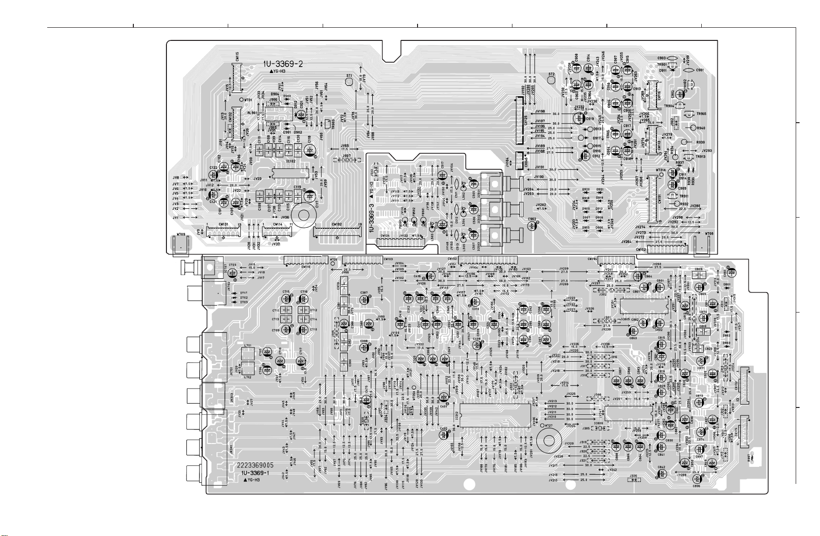
1
1U-3369 EXT IN P.W.B. Ass'y
2
11
3
4
5
76
8
A
1
13
1
1
16 9
18
12
1
11
1
10
1
1
12
1
4
1
15
1
9
14 1
15 28
10
B
C
D
42 22
14 1
COMPONENT SIDE
121
15 28
E
29
Page 31

1
1U-3369 EXT IN P.W.B. Ass'y
2
3
4
5
76
8
BE
C
C
E
B
BE
C
E
B
B
E
C
C
E
B
E
C
B
5
8
4
1
E
C
B
E
C
B
5
8
4
1
C
B
C
C
E
B
BE
C
BE
C
E
C
E
B
BE
C
8
14
7
1
E
E
C
C
B
B
5
8
B
C
E
4
1
B
C
E
1
4
5
8
1
4
5
8
1
4
5
8
9
16
8
1
9
16
8
1
5
8
4
1
5
8
4
1
5
8
4
1
A
B
C
D
5
8
5
8
4
1
5
8
4
1
4
1
E
FOIL SIDE
30
Page 32

1
1U-3370 CONTROL P.W.B. Ass'y
2
3
4
5
76
8
17
3
1
A
B
13
14
14
13
1911
2
1
14
13
2
1
18
1
2
1
8
10
1
8
9
1
1
13
2
14
15
1
2
1
8
1
1
6
11
12
12
1
7
1
1
1
C
D
2
1
13
12
2
1
9
1
15
1
10
1
11
12
1
1
E
15
1
COMPONENT SIDE
31
Page 33

1
1U-3370 CONTROL P.W.B. Ass'y
2
3
4
5
76
E
C
B
8
A
32
33
48
49
C
C
E
B
E
B
17
16
1
62
C
E
B
C
E
B
C
C
E
E
B
B
C
E
B
8
1
9
16
B
C
9
16
1
8
C
C
E
B
E
B
9
16
1
8
12
13
C
BE
E
B
C
1
24
C
E
B
BE
C
BE
C
E
B
C
BE
BE
C
C
BE
C
BE
C
E
C
B
E
C
B
75
76
100
1
51
50
26
25
D
E
FOIL SIDE
32
Page 34

1
2
1U-3371 AMP CONNECT P.W.B. Ass'y
3
4
5
76
8
1
3
1
1
7
1
1
7
4
15
9
1
1
3
5
1
9
1
132
1
15151515
1
2
10
11
1
2
2
10
11
15
11
2
18
19
11
1
1
15
A
B
C
D
1
12
2
4
14
15
E
COMPONENT SIDE
33
Page 35

1
2
1U-3371 AMP CONNECT P.W.B. Ass'y
3
4
5
76
8
A
C
B
E
E
C
B
B
C
E
E
C
B
B
C
E
E
C
B
B
C
E
E
C
B
B
C
E
C
B
E
C
B
E
B
B
B
C
C
E
E
E
C
B
B
B
C
C
E
E
E
C
B
B
B
C
C
E
B
E
E
C
C
FOIL SIDE
D
E
34
Page 36

1
1U-3373 AUDIO DSP P.W.B. Ass'y
2
3
4
5
76
8
58
44
34
33
1
10
32
17
20
11
1
10
16
1
20
11
11
10
20
1
1
16
8
9
8
1
1
16
8
8
9
45
1
14
15
28
8
14
7
1
8
1
16
16
8
9
9
45
1
8
1
6
40
7
1
17
8
14
8
14
7
1
8
1
1
8
39
29
28
18
7
10
11
1
20
1
125
101
100
1
25
51
26
50
1
1
16
16
8
9
9
1
16
8
9
1
23
11
12
22
9
16
9
9
16
16
8
1
8
8
1
1
BE
1324
12
25
1
36
37 48
4
30
1
5
29
13
21
14
20
9
1
1
8
4
5
1
8
4
4
5
C
E
B
C
E
B
C
C
B
E
E
E
C
C
B
B
15
28
14
1
15
1
8
5
11
1
16
8
9
12
B
C
E
B
C
E
B
C
E
B
C
E
B
C
E
B
C
E
B
C
E
B
C
E
B
C
E
B
C
E
B
C
E
B
C
E
B
C
E
B
C
E
B
C
E
B
C
E
1
22
16 111 17 1
1
16
1
1
16
8
8
9
8
9
58
4
4
1
15
16
9
58
4
1
114
28
121
42
A
B
C
1
4
1
4
1
8
8
4
5
5
8
1
5
D
12
1120
18
1
1
10
10
9
E
8
1
7
COMPONENT SIDE
35
Page 37

1
1U-3373 AUDIO DSP P.W.B. Ass'y
2
3
4
5
76
8
8
5
14
BE
C
BE
8
5
14
8
5
14
8
5
14
1
4
8
5
C
B
E
C
C
E
B
20
11
110
C
E
B
A
B
C
D
C
E
B
BE
C
B
C
E
E
C
B
E
C
B
B
C
E
B
C
E
FOIL SIDE
E
36
Page 38

NOTE FOR PARTS LIST
l Part indicated with the mark "" are not always in stock and possibly to take a long period of time for supplying, or in
some case supplying of part may be refused.
l When ordering of part, clearly indicate "1" and "I" (i) to avoid mis-supplying.
l Ordering part without stating its part number can not be supplied.
l Part indicated with the mark " " is not illustrated in the exploded view.
l Not including Carbon Film ±5%, 1/4W Type in the P.W.Board parts list. (Refer to the Schematic Diagram for those parts.)
WARNING:
Parts marked with this symbol
Use ONLY replacement parts recommended by the manufacturer.
have critical characteristics.
ll
Resistors
l
ll
Ex.: RN 14K 2E 182 G FR
Type Shape Power Resist- Allowable Others
and per- ance error
formance
t
RD : Carbon 2B : 1/8W F : ±1% P : Pulse-resistant type
RC : Composition 2E : 1/4W G : ±2% NL : Low noise type
RS : Metal oxide film 2H : 1/2W J : ±5% NB : Non-burning type
RW : Winding 3A : 1W K : ±10% FR : Fuse-resistor
RN : Metal film 3D : 2W M : ±20% F : Lead wire forming
RK : Metal mixture 3F : 3W
t
3H : 5W
t
t
Resistance
1 8 2 ⇒ 1800 ohm = 1.8 kohm
s
s
• Units: ohm
1 R 2 ⇒ 1.2 ohm
s
s
• Units: ohm
Indicates number of zeros after effective number.
2-digit effective number.
1-digit effective number.
2-digit effective number, decimal point indicated by R.
ll
Capacitors
l
ll
Ex.: CE 04W 1H 2R2 M BP
Type Shape Dielectric Capacity Allowable Others
and per- strength error
formance
t
CE : Aluminum foil 0J : 6.3V F : ±1% HS : High stability type
electrolytic
CA : Aluminum solid 1A : 10V G : ±2% BP : Non-polar type
electrolytic
CS : Tantalum electrolytic 1C : 16V J : ±5% HR : Ripple-resistant type
CQ : Film 1E : 25V K : ±10% DL : For change and discharge
CK : Ceramic 1V : 35V M : ±20% HF : For assuring high
CC : Ceramic 1H : 50V Z : +80% U : UL part
CP : Oil 2A : 100V –20% C : CSA part
CM : Mica 2B : 125V P : +100% W : UL-CSA type
CF : Metallized 2C : 160V –0% F : Lead wire forming
CH : Metallized 2D : 200V C : ±0.25pF
t
2E : 250V D : ±0.5pF
2H : 500V = : Others
2J : 630V
t
t
requency
Capacity (electrolyte only)
2 2 2 ⇒ 2200μF
s
s
• Units: μF.
2 R 2 ⇒ 2.2μF
s
s
• Units: μF.
Indicates number of zeros after effective number.
2-digit effective number.
1-digit effective number.
2-digit effective number, decimal point indicated by R.
Capacity (except electrolyte)
2 2 2 ⇒ 2200pF=0.0022μF
s
s
(More than 2) Indicates number of zeros after effective number.
• Units: pF.
2 2 1 ⇒ 220pF
s
s
(0 or 1) Indicates number of zeros after effective number.
• Units: pF.
• When the dielectric strength is indicated in AC, "AC" is included after the dieelectric
strength value.
2-digit effective number.
2-digit effective number.
37
Page 39

Note : The symbols in the column “Remarks” indicate the following destinations.
PARTS LIST OF P.W.B. UNIT ASS'Y
1U-3368 POWER UNIT ASS'Y
Ref. No. Part No. Part Name Remarks Ref. No. Part No. Part Name Remarks
SEMICONDUCTORS GROUP
IC501 263 1100 018 IC KIA7806API
IC502 268 0073 905 IC ICP-N15
TR101,102 273 0459 903 Transistor KTC2874B
TR103-106 271 0094 919 Transistor 2SA970(BL)
TR107,108 273 0281 906 Transistor 2SC2705(O)/(Y)
TR109,110 271 0168 900 Transistor 2SA1145 (O)/(Y)
TR111,112 273 0281 906 Transistor 2SC2705(O)/(Y)
TR117,118 273 0458 904 Transistor 2SC/KTC3200BL
TR201,202 273 0459 903 Transistor KTC2874B
TR203-206 271 0094 919 Transistor 2SA970(BL)
TR207,208 273 0281 906 Transistor 2SC2705(O)/(Y)
TR209,210 271 0168 900 Transistor 2SA1145 (O)/(Y)
TR211,212 273 0281 906 Transistor 2SC2705(O)/(Y)
TR217,218 273 0458 904 Transistor 2SC/KTC3200BL
TR301 273 0459 903 Transistor KTC2874B
TR303 271 0094 919 Transistor 2SA970(BL)
TR305 271 0094 919 Transistor 2SA970(BL)
TR307 273 0281 906 Transistor 2SC2705(O)/(Y)
TR309 271 0168 900 Transistor 2SA1145 (O)/(Y)
TR311 273 0281 906 Transistor 2SC2705(O)/(Y)
TR317 273 0458 904 Transistor 2SC/KTC3200BL
EU: U.S.A. model E1: Asia model
982: AVR-982 (U.S.A.) model E1H: Hong Kong model
EC: Canada model E1C: China model
E2: Europe model EUT: Taiwan R.O.C. model
D305 276 0432 903 Diode 1SS270A
D307 276 0432 903 Diode 1SS270A
D313 276 0432 903 Diode 1SS270A
D315 276 0432 903 Diode 1SS270A
D401 276 0432 903 Diode 1SS270A
D403 276 0432 903 Diode 1SS270A
D405 276 0432 903 Diode 1SS270A
D407 276 0432 903 Diode 1SS270A
D413 276 0432 903 Diode 1SS270A
D415 276 0432 903 Diode 1SS270A
D501,502 276 0338 007 Diode S4VB20F
D504-509 276 0704 903 Diode 1SR35-400A(T93X)
D510 276 0432 903 Diode 1SS270A
D601,602 276 0432 903 Diode 1SS270A
D604,605 276 0432 903 Diode 1SS270A
D607 276 0432 903 Diode 1SS270A
ZD101,102 276 0460 904 Zener diode HZS5C-1TD
ZD103,104 276 0461 903 Zener diode HZS6A-1TD
ZD201,202 276 0460 904 Zener diode HZS5C-1TD
ZD203,204 276 0461 903 Zener diode HZS6A-1TD
TR401 273 0459 903 Transistor KTC2874B
TR403 271 0094 919 Transistor 2SA970(BL)
TR405 271 0094 919 Transistor 2SA970(BL)
TR407 273 0281 906 Transistor 2SC2705(O)/(Y)
TR409 271 0168 900 Transistor 2SA1145 (O)/(Y)
TR411 273 0281 906 Transistor 2SC2705(O)/(Y)
TR417 273 0458 904 Transistor 2SC/KTC3200BL
TR501 271 0094 919 Transistor 2SA970(BL)
TR502 271 0131 924 Transistor 2SA988(E/F)
TR503 273 0429 904 Transistor 2SC3311A
TR504 271 0192 905 Transistor 2SA933S(S)
TR505,506 273 0429 904 Transistor 2SC3311A
TR507 271 0192 905 Transistor 2SA933S(S)
TR508,509 273 0429 904 Transistor 2SC3311A
TR510 273 0303 910 Transistor 2SC1740S(S)
TR511 269 0020 906
D101-108 276 0432 903 Diode 1SS270A
D113-116 276 0432 903 Diode 1SS270A
D201-208 276 0432 903 Diode 1SS270A
D213-216 276 0432 903 Diode 1SS270A
D301 276 0432 903 Diode 1SS270A
D303 276 0432 903 Diode 1SS270A
Transistor DTC114ES(10K-10K)
ZD301 276 0460 904 Zener diode HZS5C-1TD
ZD303 276 0461 903 Zener diode HZS6A-1TD
ZD401 276 0460 904 Zener diode HZS5C-1TD
ZD403 276 0461 903 Zener diode HZS6A-1TD
ZD503 276 0465 912 Zener diode HZS7B-2TD
ZD504 276 0645 907 Zener diode MTZJ18A
SC501 279 0016 904 Thyristor SF0R1A42
RESISTORS GROUP
R113,114 241 2379 987 Carbon film 1 kohm 1/4W(NB) RD14B2E102JNBST
R119,120 241 2379 987 Carbon film 1 kohm 1/4W(NB) RD14B2E102JNBST
R123,124 241 2378 920 Carbon film 220 ohm 1/4W(NB) RD14B2E221JNBST
R125,126 244 2671 914 Metal oxide 15 kohm 2W(NB)
R127,128 241 2378 946 Carbon film 270 ohm 1/4W(NB) RD14B2E271JNBST
R129,130 241 2378 920 Carbon film 220 ohm 1/4W(NB) RD14B2E221JNBST
R137-140 241 2376 964 Carbon film 47 ohm 1/4W(NB) RD14B2E470JNBST
R141-148 244 2671 956 Metal oxide 0.47 ohm 2W(NB)
R213,214 241 2379 987 Carbon film 1 kohm 1/4W(NB) RD14B2E102JNBST
R219,220 241 2379 987 Carbon film 1 kohm 1/4W(NB) RD14B2E102JNBST
R223,224 241 2378 920 Carbon film 220 ohm 1/4W(NB) RD14B2E221JNBST
R225,226 244 2671 914 Metal oxide 15 kohm 2W(NB)
R227,228 241 2378 946 Carbon film 270 ohm 1/4W(NB) RD14B2E271JNBST
RS14B3D153JNBST(S)
RS14B3DR47JNBST(S)
RS14B3D153JNBST(S)
38
Page 40

Ref. No. Part No. Part Name Remarks Ref. No. Part No. Part Name Remarks
R229,230 241 2378 920 Carbon film 220 ohm 1/4W(NB) RD14B2E221JNBST
R237-240 241 2376 964 Carbon film 47 ohm 1/4W(NB) RD14B2E470JNBST
R241-248 244 2671 956 Metal oxide 0.47 ohm 2W(NB)
R313 241 2379 987 Carbon film 1 kohm 1/4W(NB) RD14B2E102JNBST
R319 241 2379 987 Carbon film 1 kohm 1/4W(NB) RD14B2E102JNBST
R323 241 2378 920 Carbon film 220 ohm 1/4W(NB) RD14B2E221JNBST
R325 244 2671 914 Metal oxide 15 kohm 2W(NB)
R327 241 2378 946 Carbon film 270 ohm 1/4W(NB) RD14B2E271JNBST
R329 241 2378 920 Carbon film 220 ohm 1/4W(NB) RD14B2E221JNBST
R337 241 2376 964 Carbon film 47 ohm 1/4W(NB) RD14B2E470JNBST
R339 241 2376 964 Carbon film 47 ohm 1/4W(NB) RD14B2E470JNBST
R341 244 2671 956 Metal oxide 0.47 ohm 2W(NB)
R343 244 2671 956 Metal oxide 0.47 ohm 2W(NB)
R345 244 2671 956 Metal oxide 0.47 ohm 2W(NB)
R347 244 2671 956 Metal oxide 0.47 ohm 2W(NB)
R413 241 2379 987 Carbon film 1 kohm 1/4W(NB) RD14B2E102JNBST
R419 241 2379 987 Carbon film 1 kohm 1/4W(NB) RD14B2E102JNBST
R423 241 2378 920 Carbon film 220 ohm 1/4W(NB) RD14B2E221JNBST
R425 244 2671 914 Metal oxide 15 kohm 2W(NB)
R427 241 2378 946 Carbon film 270 ohm 1/4W(NB) RD14B2E271JNBST
R429 241 2378 920 Carbon film 220 ohm 1/4W(NB) RD14B2E221JNBST
R437 241 2376 964 Carbon film 47 ohm 1/4W(NB) RD14B2E470JNBST
R439 241 2376 964 Carbon film 47 ohm 1/4W(NB) RD14B2E470JNBST
R441 244 2671 956 Metal oxide 0.47 ohm 2W(NB)
R443 244 2671 956 Metal oxide 0.47 ohm 2W(NB)
R445 244 2671 956 Metal oxide 0.47 ohm 2W(NB)
R447 244 2671 956 Metal oxide 0.47 ohm 2W(NB)
R501 241 2387 940 Carbon film 4.7 ohm 1/4W(NB)
R502 244 2051 961 Metal oxide 100 ohm 1W
R503,504 243 2039 032 Winding 0.1 ohm 5W RW99=3H0R1K
R524 242 2009 001 Composition 2.2 Mohm 1/2W
RS14B3DR47JNBST(S)
RS14B3D153JNBST(S)
RS14B3DR47JNBST(S)
RS14B3DR47JNBST(S)
RS14B3DR47JNBST(S)
RS14B3DR47JNBST(S)
RS14B3D153JNBST(S)
RS14B3DR47JNBST(S)
RS14B3DR47JNBST(S)
RS14B3DR47JNBST(S)
RS14B3DR47JNBST(S)
RD14B2E4R7JNBST
RS14B3A101JNBST(S)
RC05GF2H225K(UL)
For EU,982,EC
VR401 211 6131 926 Semi fixed resistor 220 ohm V06PB221T
CAPACITORS GROUP
C101,102 254 4538 939 Electrolytic 47 uF/16V
254 4538 942 Electrolytic 100 uF/16V
C103,104 254 4524 985 Electrolytic 10 uF/50V
C105-108 253 1179 945 Ceramic 220 pF/50V
C109,110 255 1264 908 Mylar film 1000 pF/50V CQ93M1H102JT(B)
C111,112 253 4482 901 Ceramic 33 pF/500V CC45SL2H330JT
C113,114 254 4538 942 Electrolytic 100 uF/16V
C115,116 253 4486 907 Ceramic 47 pF/500V CC45SL2H470JT
C117,118 253 4465 902 Ceramic 5 pF/500V CC45SL2H050CT
C119,120 255 1275 942 Mylar film 220 pF/100V CQ93M2A221KT(B)
C121,122 254 4527 982 Electrolytic 10 uF/100V
C123-126 254 4527 979 Electrolytic 4.7 uF/100V
C201,202 254 4538 939 Electrolytic 47 uF/16V
254 4538 942 Electrolytic 100 uF/16V
C203,204 254 4524 985 Electrolytic 10 uF/50V
C205-208 253 1179 945 Ceramic 220 pF/50V
C209,210 255 1264 908 Mylar film 1000 pF/50V CQ93M1H102JT(B)
C211,212 253 4482 901 Ceramic 33 pF/500V CC45SL2H330JT
C213,214 254 4538 942 Electrolytic 100 uF/16V
C215,216 253 4486 907 Ceramic 47 pF/500V CC45SL2H470JT
C217,218 253 4465 902 Ceramic 5 pF/500V CC45SL2H050CT
C219,220 255 1275 942 Mylar film 220 pF/100V CQ93M2A221KT(B)
C221,222 254 4527 982 Electrolytic 10 uF/100V
C223-226 254 4527 979 Electrolytic 4.7 uF/100V
CE04W1C470MT SMG/RE3
For EU,982,EC,E1,
E1H,E1C,EUT
CE04W1C101MT SMG/RE3
For E2
CE04W1H100MT SMG/RE3
CK45B1H221KT(DD-3)
CE04W1C101MT SMG/RE3
CE04W2A100MT SMG/RE3
CE04W2A4R7MT SMG/RE3
CE04W1C470MT SMG/RE3
For EU,982,EC,
E1,E1H,E1C,EUT
CE04W1C101MT SMG/RE3
For E2
CE04W1H100MT SMG/RE3
CK45B1H221KT(DD-3)
CE04W1C101MT SMG/RE3
CE04W2A100MT SMG/RE3
CE04W2A4R7MT SMG/RE3
R611,612 244 2671 901 Metal oxide 10 ohm 2W(NB)
R630,631 244 2671 901 Metal oxide 10 ohm 2W(NB)
R634,635 244 2671 901 Metal oxide 10 ohm 2W(NB)
R713,714 244 2052 931 Metal oxide 390 ohm 1W
244 2052 960 Metal oxide 220 ohm 1W
R715,716 244 2052 960 Metal oxide 220 ohm 1W
VR101,102 211 6131 926 Semi fixed resistor 220 ohm V06PB221T
VR201,202 211 6131 926 Semi fixed resistor 220 ohm V06PB221T
VR301 211 6131 926 Semi fixed resistor 220 ohm V06PB221T
RS14B3D100JNBST(S)
RS14B3D100JNBST(S)
RS14B3D100JNBST(S)
RS14B3A391JNBST(S)
For EU,982,EC
RS14B3A221JNBST(S)
For E2,E1,E1H,E1C,EUT
RS14B3A221JNBST(S)
For E2,E1,E1H,E1C,EUT
C301 254 4538 939 Electrolytic 47 uF/16V
254 4538 942 Electrolytic 100 uF/16V
C303 254 4524 985 Electrolytic 10 uF/50V
C305 253 1179 945 Ceramic 220 pF/50V
C307 253 1179 945 Ceramic 220 pF/50V
C309 255 1264 908 Mylar film 1000 pF/50V CQ93M1H102JT(B)
C311 253 4482 901 Ceramic 33 pF/500V CC45SL2H330JT
C313 254 4538 942 Electrolytic 100 uF/16V
C315 253 4486 907 Ceramic 47 pF/500V CC45SL2H470JT
C317 253 4465 902 Ceramic 5 pF/500V CC45SL2H050CT
C319 255 1275 942 Mylar film 220 pF/100V CQ93M2A221KT(B)
C321 254 4527 982 Electrolytic 10 uF/100V
C323 254 4527 979 Electrolytic 4.7 uF/100V
C325 254 4527 979 Electrolytic 4.7 uF/100V
CE04W1C470MT SMG/RE3
For EU,982,EC,E1,E1H,E1C,EUT
CE04W1C101MT SMG/RE3
For E2
CE04W1H100MT SMG/RE3
CK45B1H221KT(DD-3)
CK45B1H221KT(DD-3)
CE04W1C101MT SMG/RE3
CE04W2A100MT SMG/RE3
CE04W2A4R7MT SMG/RE3
CE04W2A4R7MT SMG/RE3
39
Page 41

Ref. No. Part No. Part Name Remarks Ref. No. Part No. Part Name Remarks
C401 254 4538 939 Electrolytic 47 uF/16V
254 4538 942 Electrolytic 100 uF/16V
C403 254 4524 985 Electrolytic 10 uF/50V
C405 253 1179 945 Ceramic 220 pF/50V
C407 253 1179 945 Ceramic 220 pF/50V
C409 255 1264 908 Mylar film 1000 pF/50V CQ93M1H102JT(B)
C411 253 4482 901 Ceramic 33 pF/500V CC45SL2H330JT
C413 254 4538 942 Electrolytic 100 uF/16V
C415 253 4486 907 Ceramic 47 pF/500V CC45SL2H470JT
C417 253 4465 902 Ceramic 5 pF/500V CC45SL2H050CT
C419 255 1275 942 Mylar film 220 pF/100V CQ93M2A221KT(B)
C421 254 4527 982 Electrolytic 10 uF/100V
C423 254 4527 979 Electrolytic 4.7 uF/100V
C425 254 4527 979 Electrolytic 4.7 uF/100V
C502 254 4524 943 Electrolytic 1 uF/50V
C503-505 256 1042 903 Metalized 0.1 uF/250V CF93A2E104KT
C506 254 4528 729 Electrolytic 100 uF/100V
C507,508 254 6224 704 Electrolytic 10000 uF/63V
C509 253 1181 904 Ceramic 0.01 uF/50V
C510 254 4538 900 Electrolytic 10 uF/16V
C511 253 9039 906 Ceramic 0.1 uF/25V
C512 254 4533 947 Electrolytic 330 uF/6.3V
C513 253 9039 906 Ceramic 0.1 uF/25V
C514 254 4533 947 Electrolytic 330 uF/6.3V
C516 254 4538 900 Electrolytic 10 uF/16V
C517 254 4524 943 Electrolytic 1 uF/50V
C519,520 253 1181 904 Ceramic 0.01 uF/50V
C522 254 4403 721 Electrolytic 2200 uF/25V
C523 254 4524 943 Electrolytic 1 uF/50V
C524 256 1058 971 Metalized 0.1 uF/50V CF93A1H104JT (JL)
C525 253 8022 707 Ceramic 0.01 uF/250V(AC) CK45F2EAC103MC
C606,607 256 1058 939 Metalized 0.047 uF/50V CF93A1H473JT (JL)
C611-614 255 1265 936 Mylar film 0.01 uF/50V CQ93M1H103JT(B)
C616-619 253 1181 904 Ceramic 0.01 uF/50V
C627,628 256 1058 939 Metalized 0.047 uF/50V CF93A1H473JT (JL)
C629-632 255 1265 936 Mylar film 0.01 uF/50V CQ93M1H103JT(B)
C633 253 1181 904 Ceramic 0.01 uF/50V
C634,635 256 1058 939 Metalized 0.047 uF/50V CF93A1H473JT (JL)
C636-638 253 1181 904 Ceramic 0.01 uF/50V
CE04W1C470MT SMG/RE3
For EU,982,EC,
E1,E1H,E1C,EUT
CE04W1C101MT SMG/RE3
For E2
CE04W1H100MT SMG/RE3
CK45B1H221KT(DD-3)
CK45B1H221KT(DD-3)
CE04W1C101MT SMG/RE3
CE04W2A100MT SMG/RE3
CE04W2A4R7MT SMG/RE3
CE04W2A4R7MT SMG/RE3
CE04W1H010MT SMG/RE3
CE04W2A101MC SMG/RE3
CE68W1J103MC(DL)
CK45F1H103ZT(DD-3)
CE04W1C100MT SMG/RE3
CK45=1E104ZT(DD-3)
CE04W0J331MT SMG/RE3
CK45=1E104ZT(DD-3)
CE04W0J331MT SMG/RE3
CE04W1C100MT SMG/RE3
CE04W1H010MT SMG/RE3
CK45F1H103ZT(DD-3)
CE04W1E222MC (SMG)
CE04W1H010MT SMG/RE3
For E2,E1,E1H,E1C,EUT
CK45F1H103ZT(DD-3)
For E2,E1,E1H,E1C,EUT
CK45F1H103ZT(DD-3)
CK45F1H103ZT(DD-3)
OTHER PARTS GROUP
AC501 203 3976 002 AC outlet (2P)
CW031 203 4477 018 3P KR-DA connector cord 1
CW037 203 4945 045 3P KR-DA connector cord WT For EU,982,EC 1
CX021 205 0581 001 2P VH connector base For E2,E1,
CX022 205 0581 056 2P VH connector base 1
CX023 205 1093 006 2P VH connector base For E2,E1,E1H 1
CX024 205 0581 001 2P VH connector base 1
CX032 205 0841 000 3P AC connector base (BK) For E1,E1H 1
CX033 205 0825 000 3P AC connector base 1
CX037 205 0343 032 3P connector base (KR-PH) For EU,982,EC 1
CX042 205 0581 030 4P VH connector base For E1,E1H 1
CX054-058 205 0884 009 5P connector base (TUC-P) 5
CX076 205 0943 021 7P connector base (TUC-P) 1
CX077 205 1081 018 7P FJ connector base 1
CX096 205 0884 038 9P connector base (TUC-P) 1
CX102 205 0884 054 10P connector base (TUC-P) 1
F1 206 1046 001 Fuse 6.3A UL 20mm
206 1015 074 Fuse 3.15A For E2,E1C 1
206 1036 011 Fuse 6.3A For E1,E1H 1
F8 206 1046 014 Fuse 8A
206 1015 032 Fuse 2.5A For E2,E1,E1H 1
F901 206 1015 074 Fuse 3.15A For E1,E1H 1
FF501 202 0040 909 Fuse clip 1
FF502 202 0040 909 Fuse clip For EU,982,EC,
FF751 202 0040 909 Fuse clip For E1,E1H 1
FH501 202 0040 909 Fuse clip 1
FH502 202 0040 909 Fuse clip For EU,982,EC,
FH751 202 0040 909 Fuse clip For E1,E1H 1
JK601 205 1212 007 8P SP terminal 1
JK603 205 1212 007 8P SP terminal 1
JK702 204 8264 013 Head phone jack (NI)
204 8264 071 Head phone jack (Gold) For E1,E1H,
L601,602 235 0068 004 Inductor 1uH 2
L606-609 235 0068 004 Inductor 1uH 4
For EU,982,EC,EUT
E1H,E1C,EUT 1
For EU,982,EC,EUT
For EU,982,EC,EUT
E2,E1,E1H,EUT
E2,E1,E1H,EUT
For EU,982,EC,E2
E1C,EUT 1
Q'ty
1
1
1
1
1
1
C721,722 255 1264 908 Mylar film 1000 pF/50V CQ93M1H102JT(B)
For E2,E1,E1H,E1C,EUT
C723 253 9039 906 Ceramic 0.1 uF/25V
C802,803 253 1181 904 Ceramic 0.01 uF/50V
CK45=1E104ZT(DD-3)
CK45F1H103ZT(DD-3)
RL501 214 0202 009 Relay DG1U TV-8 1
RL601-603 214 0217 010 Relay (DS2SU12VDC) 3
RL604 214 0203 008 Relay (NA12W-K) 1
RL605 214 0217 010 Relay (DS2SU12VDC) 1
40
Page 42

Ref. No. Part No. Part Name Remarks
S751 212 4810 006 Slide switch For E1,E1H 1
S801 212 0373 000 Rotary encoder EC16B 1
S802,803 212 5611 903 Tact switch 2
S804 212 5611 903 Tact switch 1
S805 212 5611 903 Tact switch 1
SW901 212 0420 005 1P push switch (non lock) For EU,982,EC 1
1U-3369 EXT. IN UNIT ASS'Y
Q'ty
Ref. No. Part No. Part Name Remarks
SEMICONDUCTORS GROUP
IC102 262 2616 003 IC TC9184AP
IC103 263 0896 909 IC NJM2068MD
IC301,302 263 0896 909 IC NJM2068MD
IC308-310 263 0896 909 IC NJM2068MD
IC312 262 2919 001 IC TC9274N-017
T501 233 6073 107 Power trans. (Mini)-E3
233 6058 025 Power trans. (Mini)-E2 For E2 1
233 6278 009 Power trans. (Mini)-E1 For E1,E1H 1
233 6317 009 Power trans For E1C 1
TP101-103 205 0190 049 4P NH connector base 3
TP501 205 0190 036 3P NH connector base
W712 203 0526 002 1P contact ass'y 1
W751 203 0702 004 1P SIN-SIN wire(WHT) 1
W752 203 0702 017 1P SIN-SIN wire(RED) 1
W753 203 0702 020 1P SIN-SIN wire(YEW) 1
W755 203 0699 036 1P SIN-SIN wire(GRY) 1
W756 203 0702 033 1P SIN-SIN wire(ORG) 1
W757 203 0702 046 1P SIN-SIN wire(BLU) 1
203 5220 002 3P VH connector cord For E1,E1H 1
203 8505 009 5P VH connector cord For E1,E1H 1
513 2585 045 Fuse label
513 2654 057 Fuse label
513 2585 074 Fuse label
For EU,982,EC,EUT
For EU,982,EC,
E1,E1H,E1C,EUT
For F1 For E2,E1C
For F1 For E1,E1H
For F8 For E2,E1,E1H
1
IC501-503 269 0194 007
IC504 262 1205 907 IC TC74HCU04AF
IC505,506 262 2386 906 IC SN74HC151NS
IC701 263 0896 909 IC NJM2068MD
IC707 269 0187 001
1
IC801 263 0896 909 IC NJM2068MD For EU,982,EC
263 0898 907 IC NJM5532MD
IC802-804 263 0896 909 IC NJM2068MD
IC805 262 2662 002 IC TC9459N
IC809 262 2981 000 IC TC9482N
TR327,328 275 0100 902 Transistor 2SK771-5-TB
TR329 269 0054 901 Transistor DTC144EK
TR330 269 0055 900 Transistor DTA144EK
TR801-803 275 0100 902 Transistor 2SK771-5-TB
TR805 269 0083 901 Transistor DTA114EK
1
TR807 269 0054 901 Transistor DTC144EK
1
TR808 269 0083 901 Transistor DTA114EK
1
TR809 269 0082 902 Transistor DTC114EK
TR810 273 0460 905 Transistor KTC2875B
TR901 271 0131 924 Transistor 2SA988(E/F)
TR902 274 0160 907 Transistor 2SD2144STPU
TR903 269 0020 906
TR904,905 271 0131 924 Transistor 2SA988(E/F)
TR906-908 269 0083 901 Transistor DTA114EK
TR909 269 0083 901 Transistor DTA114EK
TR910 269 0083 901 Transistor DTA114EK
TR911 271 0131 924 Transistor 2SA988(E/F)
TR912 269 0083 901 Transistor DTA114EK
TR913 271 0131 924 Transistor 2SA988(E/F)
TR914 269 0082 902 Transistor DTC114EK
TR956 269 0083 901 Transistor DTA114EK
Optical connector GP1FA551RZ
Optical connector GP1FA551TZ
Transistor DTC114ES(10K-10K)
For E2,E1,E1H,E1C,EUT
D323,324 276 0432 903 Diode 1SS270A
D701 276 0432 903 Diode 1SS270A
D801-803 276 0432 903 Diode 1SS270A
D901-910 276 0723 900 Diode RB721Q-40 For EU,982,EC
41
Page 43

Ref. No. Part No. Part Name Remarks Ref. No. Part No. Part Name Remarks
276 0432 903 Diode 1SS270A
D911,912 276 0432 903 Diode 1SS270A
D913 276 0704 903 Diode 1SR35-400A(T93X)
D914 276 0484 919 Zener diode HZS33-2TD
D915 276 0704 903 Diode 1SR35-400A(T93X)
D916 276 0461 916 Zener diode HZS6A-2TD
D917 276 0704 903 Diode 1SR35-400A(T93X)
D918,919 276 0723 900 Diode RB721Q-40 For EU,982,EC
276 0432 903 Diode 1SS270A
RESISTORS GROUP
R101,102 247 2008 968 Carbon chip 3.3 kohm 1/16W RM73B--332JT
R103,104 247 2006 986 Carbon chip 560 ohm 1/16W RM73B--561JT
R105,106 247 2013 982 Carbon chip 470 kohm 1/16W RM73B--474JT
R107,108 247 2005 903 Carbon chip 100 ohm 1/16W RM73B--101JT
R109,110 247 2012 909 Carbon chip 82 kohm 1/16W RM73B--823JT
R111,112 247 2009 909 Carbon chip 4.7 kohm 1/16W
R113 247 2013 982 Carbon chip 470 kohm 1/16W RM73B--474JT
R114,115 247 2011 926 Carbon chip 39 kohm 1/16W RM73B--393JT
R116 247 2013 982 Carbon chip 470 kohm 1/16W RM73B--474JT
R117,118 247 2014 907 Carbon chip 560 kohm 1/16W RM73B--564JT
R119,120 247 2004 920 Carbon chip 47 ohm 1/16W RM73B--470JT
R121,122 247 2009 925 Carbon chip 5.6 kohm 1/16W RM73B--562JT
R123,124 247 2010 985 Carbon chip 27 kohm 1/16W RM73B--273JT
R125,126 247 2007 943 Carbon chip 1 kohm 1/16W RM73B--102JT
R127,128 247 2012 925 Carbon chip 100 kohm 1/16W RM73B--104JT
R141,142 247 2005 903 Carbon chip 100 ohm 1/16W RM73B--101JT
R147,148 247 2005 903 Carbon chip 100 ohm 1/16W RM73B--101JT
R319,320 247 2010 927 Carbon chip 15 kohm 1/16W RM73B--153JT
R321 247 2009 954 Carbon chip 7.5 kohm 1/16W RM73B--752JT
R325 247 2009 983 Carbon chip 10 kohm 1/16W RM73B--103JT
R327 247 2009 983 Carbon chip 10 kohm 1/16W RM73B--103JT
R333 247 2005 903 Carbon chip 100 ohm 1/16W RM73B--101JT
R334-336 247 2012 925 Carbon chip 100 kohm 1/16W RM73B--104JT
R337,338 247 2005 903 Carbon chip 100 ohm 1/16W RM73B--101JT
R339,340 247 2008 926 Carbon chip 2.2 kohm 1/16W RM73B--222JT
R341,342 247 2007 930 Carbon chip 910 ohm 1/16W RM73B--911JT
R343,344 247 2005 903 Carbon chip 100 ohm 1/16W RM73B--101JT
R345,346 247 2012 925 Carbon chip 100 kohm 1/16W RM73B--104JT
R385,386 247 2005 903 Carbon chip 100 ohm 1/16W RM73B--101JT
247 2006 960 Carbon chip 470 ohm 1/16W RM73B--471JT
R387,388 247 2015 964 Carbon chip 2.7 Mohm 1/16W RM73B--275KT
R390 247 2018 903 Carbon chip 0 ohm 1/16W RM73B--0R0KT
R401,402 247 2005 903 Carbon chip 100 ohm 1/16W RM73B--101JT
247 2006 960 Carbon chip 470 ohm 1/16W RM73B--471JT
R403,404 247 2015 964 Carbon chip 2.7 Mohm 1/16W RM73B--275KT
For E2,E1,E1H,E1C,EUT
For E2,E1,E1H,E1C,EUT
RM73B--472JT (1608)
For EU,982,EC
For E2,E1,E1H,E1C,EUT
For EU,982,EC
For E2,E1,E1H,E1C,EUT
R417,418 247 2005 903 Carbon chip 100 ohm 1/16W RM73B--101JT
R419,420 247 2015 964 Carbon chip 2.7 Mohm 1/16W RM73B--275KT
R433-438 247 2011 926 Carbon chip 39 kohm 1/16W RM73B--393JT
R439,440 247 2004 920 Carbon chip 47 ohm 1/16W RM73B--470JT
R441,442 247 2012 925 Carbon chip 100 kohm 1/16W RM73B--104JT
R445 247 2009 983 Carbon chip 10 kohm 1/16W RM73B--103JT
R446,447 247 2009 912 Carbon chip 5.1 kohm 1/16W RM73B--512JT
R448-450 247 2009 983 Carbon chip 10 kohm 1/16W RM73B--103JT
R451,452 247 2005 903 Carbon chip 100 ohm 1/16W RM73B--101JT
R453,454 247 2012 925 Carbon chip 100 kohm 1/16W RM73B--104JT
R455 247 2011 942 Carbon chip 47 kohm 1/16W RM73B--473JT
R456,457 247 2012 938 Carbon chip 110 kohm 1/16W RM73B--114JT
R458 247 2010 927 Carbon chip 15 kohm 1/16W RM73B--153JT
R459 247 2011 913 Carbon chip 36 kohm 1/16W RM73B--363JT
R460 247 2009 967 Carbon chip 8.2 kohm 1/16W RM73B--822JT
R461 247 2009 996 Carbon chip 11 kohm 1/16W RM73B--113JT
R462 247 2005 903 Carbon chip 100 ohm 1/16W RM73B--101JT
R463 247 2012 925 Carbon chip 100 kohm 1/16W RM73B--104JT
R467,468 247 2018 903 Carbon chip 0 ohm 1/16W RM73B--0R0KT
R483 247 2007 943 Carbon chip 1 kohm 1/16W RM73B--102JT
R501-503 247 2018 903 Carbon chip 0 ohm 1/16W RM73B--0R0KT
R505-507 247 2009 909 Carbon chip 4.7 kohm 1/16W
R508 247 2004 975 Carbon chip 75 ohm 1/16W RM73B--750JT
R509 247 2005 903 Carbon chip 100 ohm 1/16W RM73B--101JT
R510 247 2011 942 Carbon chip 47 kohm 1/16W RM73B--473JT
R511 247 2013 940 Carbon chip 330 kohm 1/16W RM73B--334JT
R512 247 2018 903 Carbon chip 0 ohm 1/16W RM73B--0R0KT
R514 247 2018 903 Carbon chip 0 ohm 1/16W RM73B--0R0KT
R701,702 247 2018 903 Carbon chip 0 ohm 1/16W RM73B--0R0KT
R703,704 247 2006 944 Carbon chip 390 ohm 1/16W RM73B--391JT
R705,706 247 2011 984 Carbon chip 68 kohm 1/16W RM73B--683JT
R707,708 247 2012 967 Carbon chip 150 kohm 1/16W RM73B--154JT
R709,710 247 2004 920 Carbon chip 47 ohm 1/16W RM73B--470JT
R711,712 247 2005 990 Carbon chip 240 ohm 1/16W RM73B--241JT
R713,714 247 2012 954 Carbon chip 130 kohm 1/16W RM73B--134JT
R715,716 247 2009 996 Carbon chip 11 kohm 1/16W RM73B--113JT
R717,718 247 2003 947 Carbon chip 22 ohm 1/16W RM73B--220JT
R719,720 247 2004 920 Carbon chip 47 ohm 1/16W RM73B--470JT
R721,722 247 2011 942 Carbon chip 47 kohm 1/16W RM73B--473JT
R723,724 247 2005 903 Carbon chip 100 ohm 1/16W RM73B--101JT
For EU,982,EC
247 2006 960 Carbon chip 470 ohm 1/16W RM73B--471JT
For E2,E1,E1H,E1C,EUT
RM73B--472JT (1608)
For EU,982,EC,
E1,E1H,E1C
247 2009 909 Carbon chip 4.7 kohm 1/16W
247 2006 960 Carbon chip 470 ohm 1/16W RM73B--471JT
RM73B--472JT (1608)
For E2,EUT
For EU,982,EC
For E2,E1,E1H,E1C,EUT
42
Page 44

Ref. No. Part No. Part Name Remarks Ref. No. Part No. Part Name Remarks
R725,726 247 2015 964 Carbon chip 2.7 Mohm 1/16W RM73B--275KT
R801,802 247 2011 942 Carbon chip 47 kohm 1/16W RM73B--473JT
R803,804 247 2005 903 Carbon chip 100 ohm 1/16W RM73B--101JT
R805,806 247 2007 914 Carbon chip 750 ohm 1/16W RM73B--751JT
For EU,982,EC
247 2006 986 Carbon chip 560 ohm 1/16W RM73B--561JT
For E2,E1,E1H,E1C,EUT
R807,808 247 2009 941 Carbon chip 6.8 kohm 1/16W RM73B--682JT
R809,810 247 2009 909 Carbon chip 4.7 kohm 1/16W
247 2009 925 Carbon chip 5.6 kohm 1/16W RM73B--562JT
R811,812 247 2011 942 Carbon chip 47 kohm 1/16W RM73B--473JT
R815-818 247 2012 925 Carbon chip 100 kohm 1/16W RM73B--104JT
R819,820 247 2005 903 Carbon chip 100 ohm 1/16W RM73B--101JT
R821 247 2007 914 Carbon chip 750 ohm 1/16W RM73B--751JT
247 2006 986 Carbon chip 560 ohm 1/16W RM73B--561JT
R822 247 2007 914 Carbon chip 750 ohm 1/16W RM73B--751JT
R823 247 2009 941 Carbon chip 6.8 kohm 1/16W RM73B--682JT
R824 247 2009 967 Carbon chip 8.2 kohm 1/16W RM73B--822JT
R825 247 2009 909 Carbon chip 4.7 kohm 1/16W
247 2009 925 Carbon chip 5.6 kohm 1/16W RM73B--562JT
R826 247 2013 982 Carbon chip 470 kohm 1/16W RM73B--474JT
R827,828 247 2005 903 Carbon chip 100 ohm 1/16W RM73B--101JT
R829 247 2011 942 Carbon chip 47 kohm 1/16W RM73B--473JT
R831-834 247 2012 925 Carbon chip 100 kohm 1/16W RM73B--104JT
R835,836 247 2005 903 Carbon chip 100 ohm 1/16W RM73B--101JT
R837,838 247 2007 914 Carbon chip 750 ohm 1/16W RM73B--751JT
247 2006 986 Carbon chip 560 ohm 1/16W RM73B--561JT
R839,840 247 2009 909 Carbon chip 4.7 kohm 1/16W
247 2009 925 Carbon chip 5.6 kohm 1/16W RM73B--562JT
R841,842 247 2005 903 Carbon chip 100 ohm 1/16W RM73B--101JT
R843-846 247 2012 925 Carbon chip 100 kohm 1/16W RM73B--104JT
R847,848 247 2005 903 Carbon chip 100 ohm 1/16W RM73B--101JT
R849,850 247 2007 914 Carbon chip 750 ohm 1/16W RM73B--751JT
247 2006 986 Carbon chip 560 ohm 1/16W RM73B--561JT
R851,852 247 2009 909 Carbon chip 4.7 kohm 1/16W
247 2009 925 Carbon chip 5.6 kohm 1/16W RM73B--562JT
R853,854 247 2005 903 Carbon chip 100 ohm 1/16W RM73B--101JT
RM73B--472JT (1608)
For EU,982,EC
For E2,E1,E1H,E1C,EUT
For EU,982,EC
For E2,E1,E1H,E1C,EUT
RM73B--472JT (1608)
For EU,982,EC
For E2,E1,E1H,E1C,EUT
For EU,982,EC
For E2,E1,E1H,E1C,EUT
RM73B--472JT (1608)
For EU,982,EC
For E2,E1,E1H,E1C,EUT
For EU,982,EC
For E2,E1,E1H,E1C,EUT
RM73B--472JT (1608)
For EU,982,EC
For E2,E1,E1H,E1C,EUT
R855,856 247 2012 925 Carbon chip 100 kohm 1/16W RM73B--104JT
R857 247 2009 983 Carbon chip 10 kohm 1/16W RM73B--103JT
R858 247 2007 943 Carbon chip 1 kohm 1/16W RM73B--102JT
R859,860 247 2011 942 Carbon chip 47 kohm 1/16W RM73B--473JT
R867-869 247 2011 942 Carbon chip 47 kohm 1/16W RM73B--473JT
R871,872 247 2011 942 Carbon chip 47 kohm 1/16W RM73B--473JT
R874,875 247 2011 942 Carbon chip 47 kohm 1/16W RM73B--473JT
R883-888 247 2012 925 Carbon chip 100 kohm 1/16W RM73B--104JT
R891 247 2018 903 Carbon chip 0 ohm 1/16W RM73B--0R0KT
R892 247 2007 998 Carbon chip 1.6 kohm 1/16W RM73B--162JT
R893 247 2008 926 Carbon chip 2.2 kohm 1/16W RM73B--222JT
R894 247 2011 942 Carbon chip 47 kohm 1/16W RM73B--473JT
R901-904 247 2008 926 Carbon chip 2.2 kohm 1/16W RM73B--222JT
R907 247 2014 907 Carbon chip 560 kohm 1/16W RM73B--564JT
R909 247 2004 904 Carbon chip 39 ohm 1/16W RM73B--390JT
For E2,E1,E1H,E1C,EUT
R910 247 2007 943 Carbon chip 1 kohm 1/16W RM73B--102JT
R911 247 2010 969 Carbon chip 22 kohm 1/16W RM73B--223JT
R912 247 2008 971 Carbon chip 3.6 kohm 1/16W RM73B--362JT
R913 247 2014 907 Carbon chip 560 kohm 1/16W RM73B--564JT
R914 247 2013 982 Carbon chip 470 kohm 1/16W RM73B--474JT
R915 247 2007 943 Carbon chip 1 kohm 1/16W RM73B--102JT
R916 247 2009 983 Carbon chip 10 kohm 1/16W RM73B--103JT
R917 247 2013 982 Carbon chip 470 kohm 1/16W RM73B--474JT
R918 247 2007 943 Carbon chip 1 kohm 1/16W RM73B--102JT
R919 247 2009 983 Carbon chip 10 kohm 1/16W RM73B--103JT
R920 247 2013 982 Carbon chip 470 kohm 1/16W RM73B--474JT
R921 247 2007 943 Carbon chip 1 kohm 1/16W RM73B--102JT
R922 247 2009 983 Carbon chip 10 kohm 1/16W RM73B--103JT
R923 247 2013 982 Carbon chip 470 kohm 1/16W RM73B--474JT
R924 247 2007 943 Carbon chip 1 kohm 1/16W RM73B--102JT
R925 247 2009 983 Carbon chip 10 kohm 1/16W RM73B--103JT
R926 247 2013 982 Carbon chip 470 kohm 1/16W RM73B--474JT
R927 247 2007 943 Carbon chip 1 kohm 1/16W RM73B--102JT
R928 247 2009 983 Carbon chip 10 kohm 1/16W RM73B--103JT
R929 247 2013 982 Carbon chip 470 kohm 1/16W RM73B--474JT
R930 247 2007 943 Carbon chip 1 kohm 1/16W RM73B--102JT
R931 247 2009 983 Carbon chip 10 kohm 1/16W RM73B--103JT
R932 241 2387 940 Carbon film 4.7 ohm 1/4W(NB) RD14B2E4R7JNBST
R933 247 2010 956 Carbon chip 20 kohm 1/16W RM73B--203JT
R934 244 2055 996 Metal oxide 1.2 kohm 1W
R935 247 2010 956 Carbon chip 20 kohm 1/16W RM73B--203JT
R936 241 2398 913 Carbon film 680 ohm 1/4W RD14B2E681JT(5)
R939,940 244 2055 996 Metal oxide 1.2 kohm 1W
R972 247 2013 982 Carbon chip 470 kohm 1/16W RM73B--474JT
R973 247 2007 943 Carbon chip 1 kohm 1/16W RM73B--102JT
R974 247 2009 983 Carbon chip 10 kohm 1/16W RM73B--103JT
RS14B3A122JNBST(S)
For E2,E1,E1H,E1C,EUT
RS14B3A122JNBST(S)
43
Page 45

Ref. No. Part No. Part Name Remarks Ref. No. Part No. Part Name Remarks
CAPACITORS GROUP
C101,102 254 4524 956 Electrolytic 2.2 uF/50V
C105,106 254 4524 969 Electrolytic 3.3 uF/50V
C107,108 256 1058 942 Metalized 0.056 uF/50V CF93A1H563JT (JL)
C109,110 255 1265 907 Mylar film 6800 pF/50V CQ93M1H682JT(B)
C111,112 257 0506 951 Ceramic chip 100 pF/50V CC73CH1H101JT
C113,114 255 1265 949 Mylar film 0.012 uF/50V CQ93M1H123JT(B)
C115,116 255 1264 953 Mylar film 2700 pF/50V CQ93M1H272JT(B)
C117,118 254 4524 972 Electrolytic 4.7 uF/50V
254 4538 939 Electrolytic 47 uF/16V
C119,120 255 1265 978 Mylar film 0.022 uF/50V CQ93M1H223JT(B)
C121,122 254 4524 943 Electrolytic 1 uF/50V
C309 257 0509 929 Ceramic chip 1000 pF/50V CK73B1H102KT
C310-312 254 4524 998 Electrolytic 22 uF/50V
C314 257 0504 982 Ceramic chip 47 pF/50V CC73CH1H470JT
C320 254 4524 998 Electrolytic 22 uF/50V
C323 254 4524 943 Electrolytic 1 uF/50V
C324 254 4524 943 Electrolytic 1 uF/50V
C343,344 257 0507 976 Ceramic chip 330 pF/50V CC73CH1H331JT
C345,346 254 4524 985 Electrolytic 10 uF/50V
C349,350 254 4524 998 Electrolytic 22 uF/50V
C351,352 254 4524 943 Electrolytic 1 uF/50V
C355,356 257 0507 976 Ceramic chip 330 pF/50V CC73CH1H331JT
C367,368 257 0507 976 Ceramic chip 330 pF/50V CC73CH1H331JT
C379-382 256 1058 955 Metalized 0.068 uF/50V CF93A1H683JT (JL)
C385,386 254 4524 943 Electrolytic 1 uF/50V
C387,388 254 4524 985 Electrolytic 10 uF/50V
C389,390 254 4524 943 Electrolytic 1 uF/50V
C391,392 254 4524 998 Electrolytic 22 uF/50V
C395,396 257 0504 982 Ceramic chip 47 pF/50V CC73CH1H470JT
C397,398 254 4524 998 Electrolytic 22 uF/50V
C401,402 254 4524 943 Electrolytic 1 uF/50V
C405 257 0504 908 Ceramic chip 22 pF/50V CC73CH1H220JT
C408 254 4524 998 Electrolytic 22 uF/50V
C409 257 0512 903 Ceramic chip 0.1 uF/25V CK73F1E104ZT
C410,411 254 4524 943 Electrolytic 1 uF/50V
C416 254 4524 943 Electrolytic 1 uF/50V
C502-504 257 0512 903 Ceramic chip 0.1 uF/25V CK73F1E104ZT
C505-507 254 4541 939 Electrolytic 47 uF/25V
C509 257 0512 903 Ceramic chip 0.1 uF/25V CK73F1E104ZT
C510 254 4524 969 Electrolytic 3.3 uF/50V
C514 257 0506 993 Ceramic chip 150 pF/50V CC73CH1H151JT
C516 257 0511 904 Ceramic chip 0.01 uF/50V CK73F1H103ZT
CE04W1H2R2MT SMG/RE3
CE04W1H3R3MT SMG/RE3
CE04W1H4R7MT SMG/RE3
For EU,982,EC,
E1,E1H,E1C,EUT
CE04W1C470MT SMG/RE3
For E2
CE04W1H010MT SMG/RE3
CE04W1H220MT SMG/RE3
CE04W1H220MT SMG/RE3
CE04W1H010MT SMG/RE3
CE04W1H010MT SMG/RE3
For E2,E1,E1H,E1C,EUT
CE04W1H100MT SMG/RE3
CE04W1H220MT SMG/RE3
CE04W1H010MT SMG/RE3
For E2,E1,E1H,E1C,EUT
For E2,E1,E1H,E1C,EUT
CE04W1H010MT SMG/RE3
CE04W1H100MT SMG/RE3
CE04W1H010MT SMG/RE3
CE04W1H220MT SMG/RE3
CE04W1H220MT SMG/RE3
CE04W1H010MT SMG/RE3
CE04W1H220MT SMG/RE3
CE04W1H010MT SMG/RE3
CE04W1H010MT SMG/RE3
CE04W1E470MT SMG/RE3
CE04W1H3R3MT SMG/RE3
C517 254 4524 985 Electrolytic 10 uF/50V
C518,519 257 0511 904 Ceramic chip 0.01 uF/50V CK73F1H103ZT
C703,704 257 0507 934 Ceramic chip 220 pF/50V CC73CH1H221JT
C705,706 254 4524 985 Electrolytic 10 uF/50V
C707,708 257 0506 951 Ceramic chip 100 pF/50V CC73CH1H101JT
C709,710 254 4536 931 Electrolytic 220 uF/10V
C711,712 255 4199 999 Mylar film 0.024 uF/50V
C713,714 255 1265 907 Mylar film 6800 pF/50V CQ93M1H682JT(B)
C715,716 254 4524 985 Electrolytic 10 uF/50V
C717,718 254 4524 943 Electrolytic 1 uF/50V
C719,720 257 0507 976 Ceramic chip 330 pF/50V CC73CH1H331JT
C722 257 0512 903 Ceramic chip 0.1 uF/25V CK73F1E104ZT
C723 254 4541 939 Electrolytic 47 uF/25V
C724 257 0512 903 Ceramic chip 0.1 uF/25V CK73F1E104ZT
C741 257 0512 903 Ceramic chip 0.1 uF/25V CK73F1E104ZT
C742 257 0512 903 Ceramic chip 0.1 uF/25V CK73F1E104ZT
C801,802 254 4524 985 Electrolytic 10 uF/50V
C809,810 255 1265 923 Mylar film 8200 pF/50V CQ93M1H822JT(B)
C811,812 254 4524 943 Electrolytic 1 uF/50V
C815,816 254 4524 985 Electrolytic 10 uF/50V
C823 255 1265 923 Mylar film 8200 pF/50V CQ93M1H822JT(B)
C825,826 254 4524 943 Electrolytic 1 uF/50V
C829,830 254 4524 985 Electrolytic 10 uF/50V
C837,838 254 4524 943 Electrolytic 1 uF/50V
C841,842 254 4524 985 Electrolytic 10 uF/50V
C849,850 254 4524 943 Electrolytic 1 uF/50V
C853 257 0509 929 Ceramic chip 1000 pF/50V CK73B1H102KT
C860 254 4524 943 Electrolytic 1 uF/50V
C861,862 254 4524 998 Electrolytic 22 uF/50V
254 4538 939 Electrolytic 47 uF/16V
C863,864 254 4524 943 Electrolytic 1 uF/50V
C869-871 254 4525 900 Electrolytic 33 uF/50V
254 4541 942 Electrolytic 100 uF/25V
254 4541 939 Electrolytic 47 uF/25V
C873,874 254 4525 900 Electrolytic 33 uF/50V
254 4541 942 Electrolytic 100 uF/25V
254 4541 939 Electrolytic 47 uF/25V
C881,882 254 4524 943 Electrolytic 1 uF/50V
C883-888 254 4524 998 Electrolytic 22 uF/50V
CE04W1H100MT SMG/RE3
CE04W1H100MT SMG/RE3
CE04W1A221MT SMG/RE3
CQ92M1H243JT(MRZ)
CE04W1H100MT SMG/RE3
CE04W1H010MT SMG/RE3
For E2,E1,E1H,E1C,EUT
CE04W1E470MT SMG/RE3
CE04W1H100MT SMG/RE3
CE04W1H010MT SMG/RE3
CE04W1H100MT SMG/RE3
CE04W1H010MT SMG/RE3
CE04W1H100MT SMG/RE3
CE04W1H010MT SMG/RE3
CE04W1H100MT SMG/RE3
CE04W1H010MT SMG/RE3
For E2,E1,E1H,E1C,EUT
CE04W1H010MT SMG/RE3
CE04W1H220MT SMG/RE3
For EU,982,EC,
E1,E1H,E1C,EUT
CE04W1C470MT SMG/RE3
For E2
CE04W1H010MT SMG/RE3
CE04W1H330MT SMG/RE3
For EU,982,EC
CE04W1E101MT SMG/RE3
For E2
CE04W1E470MT SMG/RE3
For E1,E1H,E1C,EUT
CE04W1H330MT SMG/RE3
For EU,982,EC
CE04W1E101MT SMG/RE3
For E2
CE04W1E470MT SMG/RE3
For E1,E1H,E1C,EUT
CE04W1H010MT SMG/RE3
CE04W1H220MT SMG/RE3
44
Page 46

1U-3370 CONTROL UNIT ASS'Y
Ref. No. Part No. Part Name Remarks Ref. No. Part No. Part Name Remarks
C896,897 254 4525 900 Electrolytic 33 uF/50V
254 4541 942 Electrolytic 100 uF/25V
254 4541 939 Electrolytic 47 uF/25V
C901 253 1181 904 Ceramic 0.01 uF/50V
C902 254 4524 956 Electrolytic 2.2 uF/50V
C903 253 1181 904 Ceramic 0.01 uF/50V
C909 254 4524 943 Electrolytic 1 uF/50V
C911 254 4527 908 Electrolytic 0.1 uF/100V
C912 254 4524 985 Electrolytic 10 uF/50V
C913,914 254 4524 901 Electrolytic 0.1 uF/50V
C915 254 4524 901 Electrolytic 0.1 uF/50V
C916-918 254 4524 901 Electrolytic 0.1 uF/50V
C919 254 4522 958 Electrolytic 100 uF/35V
C964 254 4524 901 Electrolytic 0.1 uF/50V
OTHER PARTS GROUP
CW094 205 0885 037 9P connector socket (TUC-P) 1
CW102,103 205 0885 053 10P connector socket (TUC-P) 2
CW113-116 205 1092 023 11P connector plug (TWG-P) 4
CW119 205 0885 066 11P connector socket (TUC-P) 1
CW124 205 0885 079 12P connector socket (TUC-P) 1
CW131,132 205 1092 036 13P connector plug (TWG-P) 2
CW152 205 0885 040 15P connector socket (TUC-P) 1
CW191,192 205 1092 007 19P connector plug (TWG-P) 2
CE04W1H330MT SMG/RE3
For EU,982,EC
CE04W1E101MT SMG/RE3
For E2
CE04W1E470MT SMG/RE3
For E1,E1H,E1C,EUT
CK45F1H103ZT(DD-3)
CE04W1H2R2MT SMG/RE3
CK45F1H103ZT(DD-3)
CE04W1H010MT SMG/RE3
CE04W2A0R1MT SMG/RE3
CE04W1H100MT SMG/RE3
CE04W1H0R1MT SMG/RE3
CE04W1H0R1MT SMG/RE3
CE04W1H0R1MT SMG/RE3
CE04W1V101MT SMG/RE3
CE04W1H0R1MT SMG/RE3
Q'ty
SEMICONDUCTORS GROUP
IC101 262 2549 002 IC LC75721E
IC102 499 0290 007 Remote sensor GP1U271X
IC103 262 2745 903 IC BU2090F
IC105 262 2547 907 IC LC72720NM For E2
IC303 262 2982 009 IC TMP88CU74F
IC304,305 263 1040 903 IC BU4094BCF
TR111 269 0083 901 Transistor DTA114EK
TR112 269 0055 900 Transistor DTA144EK
TR113-115 269 0054 901 Transistor DTC144EK
TR116,117 269 0055 900 Transistor DTA144EK
TR118 269 0082 902 Transistor DTC114EK
TR301 274 0163 904 Transistor 2SD601A
TR302 271 0299 905 Transistor 2SA933S(S)
TR303 269 0054 901 Transistor DTC144EK
TR304 269 0082 902 Transistor DTC114EK
TR305 269 0055 900 Transistor DTA144EK
TR306 269 0054 901 Transistor DTC144EK
TR307 269 0083 901 Transistor DTA114EK
TR308,309 269 0054 901 Transistor DTC144EK
TR401 269 0082 902 Transistor DTC114EK
TR402 269 0086 908 Transistor DTA114TK
TR403,404 269 0066 902 Transistor DTC323TK
TR405 269 0082 902 Transistor DTC114EK
TR406 273 0384 900 Transistor 2SC2412K(S) For E2
CX045 205 0884 083 4P connector base (TUC-P) 1
CX115 205 1091 024 11P connector base (TWG-P) 1
CX125 205 0884 070 12P connector base (TUC-P) 1
CX132 205 1091 037 13P connector base (TWG-P) 1
FB504-508 247 2018 903 Carbon chip 0 ohm 1/16W RM73B--0R0KT 5
FB701 247 2018 903 Carbon chip 0 ohm 1/16W RM73B--0R0KT 1
JK301 204 8513 010 6P pin jack (S-GND) 1
JK701 204 8545 004 4P pin jack (GND) 1
JK702 204 8593 001 1P pin jack (OR,NI) 1
L502 235 0060 918 Inductor 4.7uH 1
L503 235 0060 905 Inductor 2.2uH 1
L504,505 235 0060 918 Inductor 4.7uH 2
L701,702 235 9003 002 FTZ choke coil For E2,EUT 2
RL901 214 0203 008 Relay (NA12W-K) 1
W708,709 205 1034 010 M3 Screw terminal 2
W726 203 0525 003 1P SIN cord Ass'y 1
W731 203 0463 000 1P SIN con. Ass'y 1
D104 276 0468 906 Zener diode HZS9B-1TD
D109-111 276 0432 903 Diode 1SS270A
D302 276 0432 903 Diode 1SS270A
D303 276 0454 910 Zener diode HZS3C-2TD
D304 276 0432 903 Diode 1SS270A
D305,306 276 0704 903 Diode 1SR35-400A(T93X)
D401 276 0432 903 Diode 1SS270A
LD102-107 393 9434 906 LED SEL1210S
LD109,110 393 9434 906 LED SEL1210S
LD113,114 393 9452 904 LED SEL1410E
RESISTORS GROUP
R101 247 2005 903 Carbon chip 100 ohm 1/16W RM73B--101JT
R102,103 247 2006 960 Carbon chip 470 ohm 1/16W RM73B--471JT
R104-107 247 2007 927 Carbon chip 820 ohm 1/16W RM73B--821JT
R109,110 247 2007 927 Carbon chip 820 ohm 1/16W RM73B--821JT
R111 247 2005 903 Carbon chip 100 ohm 1/16W RM73B--101JT
R112 247 2007 943 Carbon chip 1 kohm 1/16W RM73B--102JT
R113 247 2005 974 Carbon chip 200 ohm 1/16W RM73B--201JT
45
Page 47

Ref. No. Part No. Part Name Remarks Ref. No. Part No. Part Name Remarks
R114 247 2006 928 Carbon chip 300 ohm 1/16W RM73B--301JT
R115 247 2006 973 Carbon chip 510 ohm 1/16W RM73B--511JT
R116 247 2007 943 Carbon chip 1 kohm 1/16W RM73B--102JT
R117-119 247 2008 955 Carbon chip 3 kohm 1/16W RM73B--302JT
R120,121 247 2007 901 Carbon chip 680 ohm 1/16W RM73B--681JT
R123,124 247 2010 956 Carbon chip 20 kohm 1/16W RM73B--203JT
R125 247 2007 943 Carbon chip 1 kohm 1/16W RM73B--102JT
R126 247 2005 974 Carbon chip 200 ohm 1/16W RM73B--201JT
R127 247 2006 928 Carbon chip 300 ohm 1/16W RM73B--301JT
R128 247 2006 973 Carbon chip 510 ohm 1/16W RM73B--511JT
R129 247 2007 943 Carbon chip 1 kohm 1/16W RM73B--102JT
R139 247 2007 943 Carbon chip 1 kohm 1/16W RM73B--102JT
R140 247 2005 903 Carbon chip 100 ohm 1/16W RM73B--101JT
R141,142 247 2009 909 Carbon chip 4.7 kohm 1/16W
R153-155 247 2011 984 Carbon chip 68 kohm 1/16W RM73B--683JT
R156,157 247 2005 903 Carbon chip 100 ohm 1/16W RM73B--101JT
R158,159 247 2011 984 Carbon chip 68 kohm 1/16W RM73B--683JT
R160 247 2009 909 Carbon chip 4.7 kohm 1/16W
R162-170 247 2011 984 Carbon chip 68 kohm 1/16W RM73B--683JT
R171 247 2009 909 Carbon chip 4.7 kohm 1/16W
R173,174 247 2011 984 Carbon chip 68 kohm 1/16W RM73B--683JT
R175,176 247 2011 942 Carbon chip 47 kohm 1/16W RM73B--473JT
R177-181 247 2011 984 Carbon chip 68 kohm 1/16W RM73B--683JT
R182 247 2009 983 Carbon chip 10 kohm 1/16W RM73B--103JT
R183-212 247 2011 984 Carbon chip 68 kohm 1/16W RM73B--683JT
R213 247 2011 942 Carbon chip 47 kohm 1/16W RM73B--473JT
R302-307 247 2009 983 Carbon chip 10 kohm 1/16W RM73B--103JT
R308 247 2005 903 Carbon chip 100 ohm 1/16W RM73B--101JT
R309,310 247 2009 983 Carbon chip 10 kohm 1/16W RM73B--103JT
R311 247 2007 943 Carbon chip 1 kohm 1/16W RM73B--102JT
R312 247 2009 983 Carbon chip 10 kohm 1/16W RM73B--103JT
R313 247 2007 943 Carbon chip 1 kohm 1/16W RM73B--102JT
R314,315 247 2009 983 Carbon chip 10 kohm 1/16W RM73B--103JT
R316 247 2005 903 Carbon chip 100 ohm 1/16W RM73B--101JT
R318 247 2005 903 Carbon chip 100 ohm 1/16W RM73B--101JT
R320 247 2005 903 Carbon chip 100 ohm 1/16W RM73B--101JT
R321 247 2009 983 Carbon chip 10 kohm 1/16W RM73B--103JT
R324-326 247 2009 909 Carbon chip 4.7 kohm 1/16W
R327 247 2009 983 Carbon chip 10 kohm 1/16W RM73B--103JT
R329 247 2009 983 Carbon chip 10 kohm 1/16W RM73B--103JT
R330 247 2005 903 Carbon chip 100 ohm 1/16W RM73B--101JT
R331 247 2009 983 Carbon chip 10 kohm 1/16W RM73B--103JT
R333,334 247 2009 983 Carbon chip 10 kohm 1/16W RM73B--103JT
R335 247 2011 942 Carbon chip 47 kohm 1/16W RM73B--473JT
R340 247 2009 909 Carbon chip 4.7 kohm 1/16W
R341,342 247 2009 983 Carbon chip 10 kohm 1/16W RM73B--103JT
R343,344 247 2005 903 Carbon chip 100 ohm 1/16W RM73B--101JT
R345 247 2018 903 Carbon chip 0 ohm 1/16W RM73B--0R0KT
R346 247 2005 903 Carbon chip 100 ohm 1/16W RM73B--101JT
RM73B--472JT (1608)
RM73B--472JT (1608)
RM73B--472JT (1608)
For E2
RM73B--472JT (1608)
RM73B--472JT (1608)
R348 247 2018 903 Carbon chip 0 ohm 1/16W RM73B--0R0KT
R349 247 2018 903 Carbon chip 0 ohm 1/16W RM73B--0R0KT
R350 247 2009 983 Carbon chip 10 kohm 1/16W RM73B--103JT
R351,352 247 2012 925 Carbon chip 100 kohm 1/16W RM73B--104JT
R354 247 2013 908 Carbon chip 220 kohm 1/16W RM73B--224JT
R355 247 2012 925 Carbon chip 100 kohm 1/16W RM73B--104JT
R356 247 2009 983 Carbon chip 10 kohm 1/16W RM73B--103JT
R357-360 247 2012 925 Carbon chip 100 kohm 1/16W RM73B--104JT
R361,362 247 2009 909 Carbon chip 4.7 kohm 1/16W
R363-365 247 2005 903 Carbon chip 100 ohm 1/16W RM73B--101JT
R366,367 247 2009 983 Carbon chip 10 kohm 1/16W RM73B--103JT
R368 247 2007 943 Carbon chip 1 kohm 1/16W RM73B--102JT
R372 247 2007 943 Carbon chip 1 kohm 1/16W RM73B--102JT
R373 247 2007 943 Carbon chip 1 kohm 1/16W RM73B--102JT
R374 247 2009 983 Carbon chip 10 kohm 1/16W RM73B--103JT
R375 241 2387 908 Carbon film 1 ohm 1/4W(NB) RD14B2E010JNBST
R376 247 2009 983 Carbon chip 10 kohm 1/16W RM73B--103JT
R378 247 2009 983 Carbon chip 10 kohm 1/16W RM73B--103JT
R379 247 2008 926 Carbon chip 2.2 kohm 1/16W RM73B--222JT
R380-383 247 2009 983 Carbon chip 10 kohm 1/16W RM73B--103JT
R384 247 2007 972 Carbon chip 1.3 kohm 1/16W RM73B--132JT
R385 247 2018 903 Carbon chip 0 ohm 1/16W RM73B--0R0KT
R387 247 2018 903 Carbon chip 0 ohm 1/16W RM73B--0R0KT
R390 247 2009 983 Carbon chip 10 kohm 1/16W RM73B--103JT
R391,392 247 2007 943 Carbon chip 1 kohm 1/16W RM73B--102JT
R393,394 247 2012 925 Carbon chip 100 kohm 1/16W RM73B--104JT
R401 247 2002 964 Carbon chip 10 ohm 1/16W RM73B--100JT
R402,403 247 2009 983 Carbon chip 10 kohm 1/16W RM73B--103JT
R404 247 2008 913 Carbon chip 2 kohm 1/16W RM73B--202JT
R406 247 2009 983 Carbon chip 10 kohm 1/16W RM73B--103JT
247 2018 903 Carbon chip 0 ohm 1/16W RM73B--0R0KT
For E2
247 2007 943 Carbon chip 1 kohm 1/16W RM73B--102JT
For E1,E1H
247 2009 909 Carbon chip 4.7 kohm 1/16W
247 2009 912 Carbon chip 5.1 kohm 1/16W RM73B--512JT
247 2009 909 Carbon chip 4.7 kohm 1/16W
247 2009 983 Carbon chip 10 kohm 1/16W RM73B--103JT
247 2012 925 Carbon chip 100 kohm 1/16W RM73B--104JT
RM73B--472JT (1608)
For E1C,EUT
For EU,982,EC
For E1,E1H
RM73B--472JT (1608)
For E1C,EUT
RM73B--472JT (1608)
For EU,982,EC
For E2,E1,E1H,E1C,EUT
For EU,982,EC
For E2,E1,E1H,E1C,EUT
For E1,E1H
For E2
For E2
For E2
46
Page 48

Ref. No. Part No. Part Name Remarks Ref. No. Part No. Part Name Remarks
R407 247 2009 909 Carbon chip 4.7 kohm 1/16W
RM73B--472JT (1608)
For E2
C392 257 0509 929 Ceramic chip 1000 pF/50V CK73B1H102KT
For EU,982,EC,E2
C398 257 0506 951 Ceramic chip 100 pF/50V CC73CH1H101JT
CAPACITORS GROUP
C102 257 0512 903 Ceramic chip 0.1 uF/25V CK73F1E104ZT
C103 254 4193 905 Electrolytic 10 uF/16V
C104 254 4196 944 Electrolytic 1 uF/50V
C107 256 1058 971 Metalized 0.1 uF/50V CF93A1H104JT (JL)
C109 254 4196 999 Electrolytic 22 uF/50V
C110-113 257 0511 904 Ceramic chip 0.01 uF/50V CK73F1H103ZT
C115 257 0511 904 Ceramic chip 0.01 uF/50V CK73F1H103ZT
C117 257 0509 929 Ceramic chip 1000 pF/50V CK73B1H102KT
C120 257 0504 937 Ceramic chip 30 pF/50V CC73CH1H300JT
C121 254 4193 905 Electrolytic 10 uF/16V
C122 257 0511 917 Ceramic chip 0.022 uF/50V CK73F1H223ZT
C125 257 0511 904 Ceramic chip 0.01 uF/50V CK73F1H103ZT
C127 254 4525 926 Electrolytic 100 uF/50V
C301 257 0509 929 Ceramic chip 1000 pF/50V CK73B1H102KT
C304 257 0516 909 Ceramic chip 0.022 uF/25V CK73B1E223KT
C309 257 0516 909 Ceramic chip 0.022 uF/25V CK73B1E223KT
C313 257 0516 909 Ceramic chip 0.022 uF/25V CK73B1E223KT
C318 257 0516 909 Ceramic chip 0.022 uF/25V CK73B1E223KT
C324 257 0516 909 Ceramic chip 0.022 uF/25V CK73B1E223KT
C339 254 4536 957 Electrolytic 470 uF/10V
C340 257 0512 903 Ceramic chip 0.1 uF/25V CK73F1E104ZT
C341 254 4538 939 Electrolytic 47 uF/16V
C342 257 0511 920 Ceramic chip 0.047 uF/50V CK73F1H473ZT
C348 254 4538 939 Electrolytic 47 uF/16V
C349 257 0511 904 Ceramic chip 0.01 uF/50V CK73F1H103ZT
C350 256 1058 984 Metalized 0.12 uF/50V CF93A1H124JT (JL)
C352 254 4522 903 Electrolytic 4.7 uF/35V
C353 257 0511 904 Ceramic chip 0.01 uF/50V CK73F1H103ZT
C354 254 4213 937 Electrolytic 100 uF/6.3V
C355 257 0511 904 Ceramic chip 0.01 uF/50V CK73F1H103ZT
C357 254 4534 713 Electrolytic 3300 uF/6.3V
259 0007 702 Back up cap. 8200 uF/5.5V SB CAP==822=C
C358 257 0509 929 Ceramic chip 1000 pF/50V CK73B1H102KT
C359 254 4533 934 Electrolytic 220 uF/6.3V
C376 257 0509 929 Ceramic chip 1000 pF/50V CK73B1H102KT
C377 254 4538 900 Electrolytic 10 uF/16V
C378 257 0509 929 Ceramic chip 1000 pF/50V CK73B1H102KT
C380 257 0516 909 Ceramic chip 0.022 uF/25V CK73B1E223KT
C390 256 1058 971 Metalized 0.1 uF/50V CF93A1H104JT (JL)
CE04W1C100MT (SRA)
CE04W1H010MT (SRA)
CE04W1H220MT (SRA)
CE04W1C100MT (SRA)
CE04W1H101MT SMG/RE3
For E1,E1H,E1C,EUT
For EU,982,EC,E2
For E1,E1H,E1C,EUT
For EU,982,EC,E2
CE04W1A471MT SMG/RE3
CE04W1C470MT SMG/RE3
CE04W1C470MT SMG/RE3
CE04W1V4R7MT SMG/RE3
CE04W0J101MT (SRA)
CE04W0J332MC SMG/RE3
For EU,982,EC
For E2,E1,E1H,E1C,EUT
CE04W0J221MT SMG/RE3
CE04W1C100MT SMG/RE3
For EU,982,EC,E2
C400 254 4538 900 Electrolytic 10 uF/16V
C401 257 0511 904 Ceramic chip 0.01 uF/50V CK73F1H103ZT
C405 257 0516 909 Ceramic chip 0.022 uF/25V CK73B1E223KT
C411,412 257 0504 924 Ceramic chip 27 pF/50V CC73CH1H270JT
C416 257 0516 909 Ceramic chip 0.022 uF/25V CK73B1E223KT
257 0509 929 Ceramic chip 1000 pF/50V CK73B1H102KT
C417,418 254 4524 943 Electrolytic 1 uF/50V
C419 254 4538 900 Electrolytic 10 uF/16V
C420 257 0516 909 Ceramic chip 0.022 uF/25V CK73B1E223KT
257 0509 929 Ceramic chip 1000 pF/50V CK73B1H102KT
C421 257 0508 933 Ceramic chip 560 pF/50V CC73CH1H561JT
C423,424 254 4524 985 Electrolytic 10 uF/50V
C492 257 0509 929 Ceramic chip 1000 pF/50V CK73B1H102KT
C493 257 0507 976 Ceramic chip 330 pF/50V CC73CH1H331JT
C983 257 0516 909 Ceramic chip 0.022 uF/25V CK73B1E223KT
OTHER PARTS GROUP
CW077 205 1000 015 7P FJ connector plug 1
CW142,143 205 1165 002 14P connector plug (TMC-D) 2
CX061 205 0943 018 6P connector base (TUC-P) 1
CX072 205 0943 021 7P connector base (TUC-P) 1
CX081,082 205 0884 096 8P connector base (TUC-P) 2
CX086 205 0884 096 8P connector base (TUC-P) 1
CX093,094 205 0884 038 9P connector base (TUC-P) 2
CX103 205 0884 054 10P connector base (TUC-P) 1
CX111 205 0884 067 11P connector base (TUC-P) 1
CX114 205 1091 024 11P connector base (TWG-P) 1
CX119 205 0884 067 11P connector base (TUC-P) 1
CX121,122 205 0884 070 12P connector base (TUC-P) 2
CX124 205 0884 070 12P connector base (TUC-P) 1
CX131 205 1091 037 13P connector base (TWG-P) 1
CX142,143 205 1164 003 14P connector socket (TMC-D) 2
CX151 205 0884 041 15P connector base (TUC-P) 1
CX152,153 205 0884 041 15P connector base (TUC-P) 2
CX192 205 1091 008 19P connector base (TWG-P) 1
CX932 205 1121 033 3P connector base-L (5268) 1
CE04W1C100MT SMG/RE3
For E2
For EU,982,EC,
E1,E1H,E1C,EUT
For E2
CE04W1H010MT SMG/RE3
For E2
CE04W1C100MT SMG/RE3
For E2
For EU,982,EC
For E2
For E2
CE04W1H100MT SMG/RE3
For E2
Q'ty
47
Page 49

Ref. No. Part No. Part Name Remarks
FB304,305 235 0049 900 Beads inductor 2
FL101 393 8033 007 FLD (CM1690C) 1
L101 235 0070 995 Inductor 220uH 1
L102 235 0070 953 Inductor 68uH 1
L308 247 2005 987 Carbon chip 220 ohm 1/16W RM73B--221JT 1
L313-315 247 2005 987 Carbon chip 220 ohm 1/16W RM73B--221JT 3
L319 247 2005 987 Carbon chip 220 ohm 1/16W RM73B--221JT 1
S101-112 212 5611 903 Tact switch 12
S113 212 0373 000 Rotary encoder EC16B 1
S114 212 0422 003 Rotary encoder 1
S115 212 5611 903 Tact switch 1
W724 203 0526 002 1P contact ass'y 1
XL302 399 0532 902 Ceramic 12.5 MHz
XL401 399 0178 007 Crystal 4.332 MHz For E2 1
CST12.5MTW-TF01
1U-3371 REGULATOR UNIT ASS'Y
Q'ty
Ref. No. Part No. Part Name Remarks
SEMICONDUCTORS GROUP
IC901,902 263 1100 005 IC KIA7805API
IC905 263 1100 021 IC KIA7812API
IC906 263 1099 022 IC KIA7912PI
IC907 263 1100 005 IC KIA7805API
IC909 263 1099 006 IC KIA7905PI
TR501-504 273 0460 905 Transistor KTC2875B
TR511-514 273 0460 905 Transistor KTC2875B
TR521-524 273 0460 905 Transistor KTC2875B
TR531-534 273 0460 905 Transistor KTC2875B
TR541-544 273 0460 905 Transistor KTC2875B
TR581,582 273 0429 904 Transistor 2SC3311A
TR584 269 0020 906
TR585,586 273 0429 904 Transistor 2SC3311A
TR901 273 0429 904 Transistor 2SC3311A
TR904 272 0158 007 Transistor 2SB/KTB778(R/O)
1
TR918 272 0158 007 Transistor 2SB/KTB778(R/O)
D903,904 276 0432 903 Diode 1SS270A
D913-915 276 0305 001 Diode S4VB20
D918,919 276 0432 903 Diode 1SS270A
Transistor DTC114ES(10K-10K)
PT901 279 0034 054
RESISTORS GROUP
R501-504 247 2006 960 Carbon chip 470 ohm 1/16W RM73B--471JT
247 2006 973 Carbon chip 510 ohm 1/16W RM73B--511JT
R505,506 247 2012 925 Carbon chip 100 kohm 1/16W RM73B--104JT
247 2008 984 Carbon chip 3.9 kohm 1/16W RM73B--392JT
R507,508 247 2009 983 Carbon chip 10 kohm 1/16W RM73B--103JT
R509,510 247 2010 969 Carbon chip 22 kohm 1/16W RM73B--223JT
R511 247 2006 960 Carbon chip 470 ohm 1/16W RM73B--471JT
247 2006 973 Carbon chip 510 ohm 1/16W RM73B--511JT
R512 247 2006 960 Carbon chip 470 ohm 1/16W RM73B--471JT
R513 247 2006 960 Carbon chip 470 ohm 1/16W RM73B--471JT
247 2006 973 Carbon chip 510 ohm 1/16W RM73B--511JT
R514 247 2006 960 Carbon chip 470 ohm 1/16W RM73B--471JT
R515 247 2012 925 Carbon chip 100 kohm 1/16W RM73B--104JT
247 2008 984 Carbon chip 3.9 kohm 1/16W RM73B--392JT
R516 247 2012 925 Carbon chip 100 kohm 1/16W RM73B--104JT
R517,518 247 2009 983 Carbon chip 10 kohm 1/16W RM73B--103JT
Posistor PTH9M04BC222TS2F333
For EU,982,EC
For E2,E1,E1H,E1C,EUT
For EU,982,EC
For E2,E1,E1H,E1C,EUT
For EU,982,EC
For E2,E1,E1H,E1C,EUT
For EU,982,EC
For E2,E1,E1H,E1C,EUT
For EU,982,EC
For E2,E1,E1H,E1C,EUT
48
Page 50

Ref. No. Part No. Part Name Remarks Ref. No. Part No. Part Name Remarks
R519,520 247 2010 969 Carbon chip 22 kohm 1/16W RM73B--223JT
R521-524 247 2006 960 Carbon chip 470 ohm 1/16W RM73B--471JT
For EU,982,EC
247 2006 973 Carbon chip 510 ohm 1/16W RM73B--511JT
For E2,E1,E1H,E1C,EUT
R525,526 247 2012 925 Carbon chip 100 kohm 1/16W RM73B--104JT
For EU,982,EC
247 2008 984 Carbon chip 3.9 kohm 1/16W RM73B--392JT
For E2,E1,E1H,E1C,EUT
R527,528 247 2009 983 Carbon chip 10 kohm 1/16W RM73B--103JT
R529,530 247 2010 969 Carbon chip 22 kohm 1/16W RM73B--223JT
R531-534 247 2006 960 Carbon chip 470 ohm 1/16W RM73B--471JT
For EU,982,EC
247 2006 973 Carbon chip 510 ohm 1/16W RM73B--511JT
For E2,E1,E1H,E1C,EUT
R535,536 247 2012 925 Carbon chip 100 kohm 1/16W RM73B--104JT
For EU,982,EC
247 2008 984 Carbon chip 3.9 kohm 1/16W RM73B--392JT
For E2,E1,E1H,E1C,EUT
R537,538 247 2009 983 Carbon chip 10 kohm 1/16W RM73B--103JT
R539,540 247 2010 969 Carbon chip 22 kohm 1/16W RM73B--223JT
R541-544 247 2006 960 Carbon chip 470 ohm 1/16W RM73B--471JT
R545,546 247 2012 925 Carbon chip 100 kohm 1/16W RM73B--104JT
R547,548 247 2009 983 Carbon chip 10 kohm 1/16W RM73B--103JT
R549,550 247 2010 969 Carbon chip 22 kohm 1/16W RM73B--223JT
R551,552 247 2012 925 Carbon chip 100 kohm 1/16W RM73B--104JT
For EU,982,EC
247 2009 909 Carbon chip 4.7 kohm 1/16W
R553,554 247 2005 987 Carbon chip 220 ohm 1/16W RM73B--221JT
R555 247 2012 925 Carbon chip 100 kohm 1/16W RM73B--104JT
247 2009 909 Carbon chip 4.7 kohm 1/16W
R556 247 2012 925 Carbon chip 100 kohm 1/16W RM73B--104JT
R557,558 247 2005 987 Carbon chip 220 ohm 1/16W RM73B--221JT
R559,560 247 2012 925 Carbon chip 100 kohm 1/16W RM73B--104JT
247 2009 909 Carbon chip 4.7 kohm 1/16W
R561,562 247 2005 987 Carbon chip 220 ohm 1/16W RM73B--221JT
R563,564 247 2012 925 Carbon chip 100 kohm 1/16W RM73B--104JT
247 2009 909 Carbon chip 4.7 kohm 1/16W
R565,566 247 2005 987 Carbon chip 220 ohm 1/16W RM73B--221JT
R567,568 247 2012 925 Carbon chip 100 kohm 1/16W RM73B--104JT
R569,570 247 2005 987 Carbon chip 220 ohm 1/16W RM73B--221JT
R586-594 247 2018 903 Carbon chip 0 ohm 1/16W RM73B--0R0KT
RM73B--472JT (1608)
For E2,E1,E1H,E1C,EUT
For EU,982,EC
RM73B--472JT (1608)
For E2,E1,E1H,E1C,EUT
For EU,982,EC
RM73B--472JT (1608)
For E2,E1,E1H,E1C,EUT
For EU,982,EC
RM73B--472JT (1608)
For E2,E1,E1H,E1C,EUT
CAPACITORS GROUP
C501-504 254 4538 913 Electrolytic 22 uF/16V
254 4538 942 Electrolytic 100 uF/16V
C507 254 4524 943 Electrolytic 1 uF/50V
C511 254 4538 913 Electrolytic 22 uF/16V
254 4538 942 Electrolytic 100 uF/16V
C512 254 4538 913 Electrolytic 22 uF/16V
C513 254 4538 913 Electrolytic 22 uF/16V
254 4538 942 Electrolytic 100 uF/16V
C514 254 4538 913 Electrolytic 22 uF/16V
C521-524 254 4538 913 Electrolytic 22 uF/16V
254 4538 942 Electrolytic 100 uF/16V
C527 254 4524 943 Electrolytic 1 uF/50V
C531-534 254 4538 913 Electrolytic 22 uF/16V
254 4538 942 Electrolytic 100 uF/16V
C541-544 254 4538 913 Electrolytic 22 uF/16V
C591,592 254 4524 943 Electrolytic 1 uF/50V
C901 253 1181 904 Ceramic 0.01 uF/50V
C902 254 4541 939 Electrolytic 47 uF/25V
C903 254 4538 939 Electrolytic 47 uF/16V
C904 253 9039 906 Ceramic 0.1 uF/25V
C906 253 1181 904 Ceramic 0.01 uF/50V
C908 254 4538 939 Electrolytic 47 uF/16V
C910 253 1181 904 Ceramic 0.01 uF/50V
C911 254 4538 939 Electrolytic 47 uF/16V
C916,917 254 4541 939 Electrolytic 47 uF/25V
C927 254 4472 707 Electrolytic 4700 uF/16V
C930 253 1181 904 Ceramic 0.01 uF/50V
C931 254 4406 702 Electrolytic 3300 uF/16V
C934 254 4403 734 Electrolytic 4700 uF/25V
C935 254 4403 718 Electrolytic 1000 uF/25V
C936-939 256 1058 971 Metalized 0.1 uF/50V CF93A1H104JT (JL)
C940,941 256 1058 971 Metalized 0.1 uF/50V CF93A1H104JT (JL)
C942 254 4538 939 Electrolytic 47 uF/16V
C948 254 4539 718 Electrolytic 2200 uF/16V
C952 254 4524 943 Electrolytic 1 uF/50V
CE04W1C220MT SMG/RE3
For EU,982,EC
CE04W1C101MT SMG/RE3
For E2,E1,E1H,E1C,EUT
CE04W1H010MT SMG/RE3
CE04W1C220MT SMG/RE3
For EU,982,EC
CE04W1C101MT SMG/RE3
For E2,E1,E1H,E1C,EUT
CE04W1C220MT SMG/RE3
CE04W1C220MT SMG/RE3
For EU,982,EC
CE04W1C101MT SMG/RE3
For E2,E1,E1H,E1C,EUT
CE04W1C220MT SMG/RE3
CE04W1C220MT SMG/RE3
For EU,982,EC
CE04W1C101MT SMG/RE3
For E2,E1,E1H,E1C,EUT
CE04W1H010MT SMG/RE3
CE04W1C220MT SMG/RE3
For EU,982,EC
CE04W1C101MT SMG/RE3
For E2,E1,E1H,E1C,EUT
CE04W1C220MT SMG/RE3
CE04W1H010MT SMG/RE3
CK45F1H103ZT(DD-3)
CE04W1E470MT SMG/RE3
CE04W1C470MT SMG/RE3
CK45=1E104ZT(DD-3)
CK45F1H103ZT(DD-3)
CE04W1C470MT SMG/RE3
CK45F1H103ZT(DD-3)
CE04W1C470MT SMG/RE3
CE04W1E470MT SMG/RE3
CE04W1C472MC (SMG)
CK45F1H103ZT(DD-3)
CE04W1C332MC(SMG)
CE04W1E472MC(SMG)
CE04W1E102MC (SMG)
CE04W1C470MT SMG/RE3
CE04W1C222MC SMG/RE3
CE04W1H010MT SMG/RE3
R910 241 2376 919 Carbon film 30 ohm 1/4W(NB) RD14B2E300JNBST
R949 241 2376 919 Carbon film 30 ohm 1/4W(NB) RD14B2E300JNBST
49
Page 51

Ref. No. Part No. Part Name Remarks
OTHER PARTS GROUP
CW045 205 0885 082 4P connector socket (TUC-P) 1
CW054-058 205 0885 008 5P connector socket (TUC-P) 5
CW076 205 0942 022 7P connector socket (TUC-P) 1
CW096 205 0885 037 9P connector socket (TUC-P) 1
CW125 205 0885 079 12P connector socket (TUC-P) 1
CW151 205 0885 040 15P connector socket (TUC-P) 1
CW154 205 0885 040 15P connector socket (TUC-P) 1
CX031 205 0321 038
CX073 205 0343 074 7P connector base (KR-PH) 1
CX091 205 0233 090 9P EH connector base 1
CX113 205 1091 024 11P connector base (TWG-P) 1
CX116 205 1091 024 11P connector base (TWG-P) 1
CX154 205 0884 041 15P connector base (TUC-P) 1
CX159 205 0770 045 15P FFC base (SIDE) 1
CX191 205 1091 008 19P connector base (TWG-P) 1
3P connector base (KR-PH RED)
1U-3373 DSP/VIDEO UNIT ASS'Y
Q’ty
Ref. No. Part No. Part Name Remarks
SEMICONDUCTORS GROUP
IC107 262 2545 006 IC TC9274N-011
IC108 262 2033 000 IC TC9273N-004
IC109 263 0896 909 IC NJM2068MD
IC112 263 0615 902 IC BA15218F
IC251,252 262 2826 903 IC BU4051BCF
IC253,254 263 1082 903 IC TK15420MTL
IC255 262 2012 908 IC BU4052BCFT1
IC256 262 2013 907 IC BU4053BCFT1
1
IC257 263 1082 903 IC TK15420MTL
IC301 262 2983 105 IC TMP93CS40F
IC451 262 2827 902 IC MM74HC4053SJ
IC452 263 0682 003 IC NJM2229S
IC453 262 2808 002 IC M35015-210SP
CY021 205 0581 001 2P VH connector base For E2,E1,
E1H,E1C,EUT 1
F11-15 206 1039 076 Fuse 2.5A For EU,982,
EC,EUT 5
206 1015 032 Fuse 2.5A For E2,E1,
E1H,E1C 5
FF901-905 202 0040 909 Fuse clip 5
FH901-905 202 0040 909 Fuse clip 5
JK501 204 8543 006 6P pin jack 1
JK502 204 8540 009 4P pin jack 1
S901 212 1030 009 Power switch (TV-5) For E2,E1,
E1H,E1C,EUT 1
ST101
ST501 205 1034 010 M3 Screw terminal 1
⎯
Style pin 1
415 0309 026 P.V.C. tube(L=20) For PT901 1
513 2585 074 Fuse label For F11-15
For E2,E1,E1H,E1C
IC501-503 263 1082 903 IC TK15420MTL
IC504-507 262 2826 903 IC BU4051BCF
IC508 263 1082 903 IC TK15420MTL
IC509,510 262 2012 908 IC BU4052BCFT1
IC511 263 1082 903 IC TK15420MTL
IC601 262 2747 901 IC AD1854JRSRL
IC602 262 2950 002 IC AK4527BVQ
IC701 263 0896 909 IC NJM2068MD
IC721 263 0896 909 IC NJM2068MD
IC741 263 0896 909 IC NJM2068MD
IC761 263 0896 909 IC NJM2068MD
IC800 262 2675 015 IC LC89055W
IC801 262 2608 901 IC TC74VHC123AFT
IC804 262 2870 904 IC 74LVX157MTC
IC807 262 2519 906 IC SN74LV00APW-EL2
IC809 262 2557 900 IC SN74LV14APW-EL2
IC811,812 263 0934 900 IC BA4510F
IC813 262 2781 909 IC SN74LV4040APW
IC814 262 2949 903 IC CS493292-CL
IC815,816 262 2660 907 IC SN74AHC574PW
IC817 262 3010 006 IC AT49LV002-70TC
5
IC818 262 2959 906 IC SN74LV244APW
IC819 263 1048 002 IC BA033T
IC823 262 2376 903 IC TC74HCT7007AF
IC824 263 1129 905 IC NJM2391DL1
IC825 262 2959 906 IC SN74LV244APW
TR305 269 0082 902 Transistor DTC114EK
TR453,454 269 0048 904 Transistor DTC143EK
TR455,456 273 0384 900 Transistor 2SC2412K(S)
50
Page 52

Ref. No. Part No. Part Name Remarks Ref. No. Part No. Part Name Remarks
TR501 271 0300 904 Transistor KTA1266GR
TR502 269 0020 906
TR503 269 0082 902 Transistor DTC114EK
TR601 269 0083 901 Transistor DTA114EK
TR602 269 0082 902 Transistor DTC114EK
TR603-607 269 0083 901 Transistor DTA114EK
TR701-704 273 0460 905 Transistor KTC2875B
TR721-724 273 0460 905 Transistor KTC2875B
TR741-744 273 0460 905 Transistor KTC2875B
TR761-764 273 0460 905 Transistor KTC2875B
D251,252 276 0559 909 Diode DAP202KT146
D453 276 0560 901 Diode DAN202KT146
D457,458 276 0559 909 Diode DAP202KT146
D459 276 0559 909 Diode DAP202KT146
D501,502 276 0559 909 Diode DAP202KT146
D601 276 0560 901 Diode DAN202KT146
D603 276 0560 901 Diode DAN202KT146
RESISTORS GROUP
R101,102 247 2005 903 Carbon chip 100 ohm 1/16W RM73B--101JT
247 2006 960 Carbon chip 470 ohm 1/16W RM73B--471JT
R103,104 247 2015 964 Carbon chip 2.7 Mohm 1/16W RM73B--275KT
R113,114 247 2005 903 Carbon chip 100 ohm 1/16W RM73B--101JT
247 2006 960 Carbon chip 470 ohm 1/16W RM73B--471JT
R115,116 247 2015 964 Carbon chip 2.7 Mohm 1/16W RM73B--275KT
R125,126 247 2005 903 Carbon chip 100 ohm 1/16W RM73B--101JT
247 2006 960 Carbon chip 470 ohm 1/16W RM73B--471JT
R127,128 247 2015 964 Carbon chip 2.7 Mohm 1/16W RM73B--275KT
R137,138 247 2005 903 Carbon chip 100 ohm 1/16W RM73B--101JT
247 2006 960 Carbon chip 470 ohm 1/16W RM73B--471JT
R139,140 247 2015 964 Carbon chip 2.7 Mohm 1/16W RM73B--275KT
R149,150 247 2005 903 Carbon chip 100 ohm 1/16W RM73B--101JT
247 2006 960 Carbon chip 470 ohm 1/16W RM73B--471JT
R151,152 247 2015 964 Carbon chip 2.7 Mohm 1/16W RM73B--275KT
R161,162 247 2005 903 Carbon chip 100 ohm 1/16W RM73B--101JT
Transistor DTC114ES(10K-10K)
For EU,982,EC
For E2,E1,E1H,E1C,EUT
For EU,982,EC
For E2,E1,E1H,E1C,EUT
For EU,982,EC
For E2,E1,E1H,E1C,EUT
For EU,982,EC
For E2,E1,E1H,E1C,EUT
For EU,982,EC
For E2,E1,E1H,E1C,EUT
For EU,982,EC
R163,164 247 2015 964 Carbon chip 2.7 Mohm 1/16W RM73B--275KT
R173,174 247 2015 964 Carbon chip 2.7 Mohm 1/16W RM73B--275KT
R175,176 247 2006 960 Carbon chip 470 ohm 1/16W RM73B--471JT
R177,178 247 2015 964 Carbon chip 2.7 Mohm 1/16W RM73B--275KT
R179,180 247 2006 960 Carbon chip 470 ohm 1/16W RM73B--471JT
R181,182 247 2015 964 Carbon chip 2.7 Mohm 1/16W RM73B--275KT
R183,184 247 2006 960 Carbon chip 470 ohm 1/16W RM73B--471JT
R187-190 247 2012 996 Carbon chip 200 kohm 1/16W RM73B--204JT
R191,192 247 2005 903 Carbon chip 100 ohm 1/16W RM73B--101JT
R195,196 247 2018 903 Carbon chip 0 ohm 1/16W RM73B--0R0KT
R197-200 247 2005 903 Carbon chip 100 ohm 1/16W RM73B--101JT
R201,202 247 2012 925 Carbon chip 100 kohm 1/16W RM73B--104JT
R203-206 247 2012 996 Carbon chip 200 kohm 1/16W RM73B--204JT
R207-210 247 2005 903 Carbon chip 100 ohm 1/16W RM73B--101JT
R235,236 247 2018 903 Carbon chip 0 ohm 1/16W RM73B--0R0KT
R251-255 247 2004 975 Carbon chip 75 ohm 1/16W RM73B--750JT
R256-258 247 2010 969 Carbon chip 22 kohm 1/16W RM73B--223JT
R259-261 247 2004 975 Carbon chip 75 ohm 1/16W RM73B--750JT
R263 247 2005 903 Carbon chip 100 ohm 1/16W RM73B--101JT
R264 247 2009 983 Carbon chip 10 kohm 1/16W RM73B--103JT
R265 247 2006 973 Carbon chip 510 ohm 1/16W RM73B--511JT
R266 247 2006 986 Carbon chip 560 ohm 1/16W RM73B--561JT
R268 247 2002 964 Carbon chip 10 ohm 1/16W RM73B--100JT
R269-271 247 2008 913 Carbon chip 2 kohm 1/16W RM73B--202JT
R275-277 247 2009 983 Carbon chip 10 kohm 1/16W RM73B--103JT
R278-280 247 2005 903 Carbon chip 100 ohm 1/16W RM73B--101JT
R281 247 2009 983 Carbon chip 10 kohm 1/16W RM73B--103JT
R282,283 247 2005 903 Carbon chip 100 ohm 1/16W RM73B--101JT
R284 247 2009 983 Carbon chip 10 kohm 1/16W RM73B--103JT
R285 247 2008 913 Carbon chip 2 kohm 1/16W RM73B--202JT
R286 247 2006 973 Carbon chip 510 ohm 1/16W RM73B--511JT
R287 247 2006 999 Carbon chip 620 ohm 1/16W RM73B--621JT
R291 247 2009 983 Carbon chip 10 kohm 1/16W RM73B--103JT
R292 247 2002 964 Carbon chip 10 ohm 1/16W RM73B--100JT
R293 247 2018 903 Carbon chip 0 ohm 1/16W RM73B--0R0KT
R301,302 247 2009 983 Carbon chip 10 kohm 1/16W RM73B--103JT
R303 247 2003 989 Carbon chip 33 ohm 1/16W RM73B--330JT
R304 247 2009 909 Carbon chip 4.7 kohm 1/16W
R305,306 247 2003 989 Carbon chip 33 ohm 1/16W RM73B--330JT
R307 247 2009 983 Carbon chip 10 kohm 1/16W RM73B--103JT
R308 247 2003 989 Carbon chip 33 ohm 1/16W RM73B--330JT
R309 247 2009 983 Carbon chip 10 kohm 1/16W RM73B--103JT
R311,312 247 2003 989 Carbon chip 33 ohm 1/16W RM73B--330JT
R313 247 2009 983 Carbon chip 10 kohm 1/16W RM73B--103JT
R314-327 247 2003 989 Carbon chip 33 ohm 1/16W RM73B--330JT
R328 247 2009 983 Carbon chip 10 kohm 1/16W RM73B--103JT
R331 247 2018 903 Carbon chip 0 ohm 1/16W RM73B--0R0KT
R334 247 2018 903 Carbon chip 0 ohm 1/16W RM73B--0R0KT
247 2006 960 Carbon chip 470 ohm 1/16W RM73B--471JT
For E2,E1,E1H,E1C,EUT
RM73B--472JT (1608)
51
Page 53

Ref. No. Part No. Part Name Remarks Ref. No. Part No. Part Name Remarks
R336 247 2009 983 Carbon chip 10 kohm 1/16W RM73B--103JT
R337 247 2011 942 Carbon chip 47 kohm 1/16W RM73B--473JT
R338 247 2009 983 Carbon chip 10 kohm 1/16W RM73B--103JT
R342 247 2009 983 Carbon chip 10 kohm 1/16W RM73B--103JT
R345,346 247 2018 903 Carbon chip 0 ohm 1/16W RM73B--0R0KT
R348-351 247 2009 983 Carbon chip 10 kohm 1/16W RM73B--103JT
R452 247 2018 903 Carbon chip 0 ohm 1/16W RM73B--0R0KT
R453 247 2008 926 Carbon chip 2.2 kohm 1/16W RM73B--222JT
R454 247 2007 943 Carbon chip 1 kohm 1/16W RM73B--102JT
R455 247 2008 900 Carbon chip 1.8 kohm 1/16W RM73B--182JT
R456 247 2002 964 Carbon chip 10 ohm 1/16W RM73B--100JT
R457 247 2009 983 Carbon chip 10 kohm 1/16W RM73B--103JT
R458 247 2007 943 Carbon chip 1 kohm 1/16W RM73B--102JT
R459 247 2013 982 Carbon chip 470 kohm 1/16W RM73B--474JT
R460 247 2011 900 Carbon chip 33 kohm 1/16W RM73B--333JT
R461 247 2006 944 Carbon chip 390 ohm 1/16W RM73B--391JT
R462 247 2007 985 Carbon chip 1.5 kohm 1/16W RM73B--152JT
R463 247 2009 983 Carbon chip 10 kohm 1/16W RM73B--103JT
R464 247 2011 955 Carbon chip 51 kohm 1/16W RM73B--513JT
R465 247 2009 954 Carbon chip 7.5 kohm 1/16W RM73B--752JT
R466 247 2018 903 Carbon chip 0 ohm 1/16W RM73B--0R0KT
R468 247 2018 903 Carbon chip 0 ohm 1/16W RM73B--0R0KT
R469-477 247 2012 925 Carbon chip 100 kohm 1/16W RM73B--104JT
R478-480 247 2018 903 Carbon chip 0 ohm 1/16W RM73B--0R0KT
R482 247 2018 903 Carbon chip 0 ohm 1/16W RM73B--0R0KT
R483 247 2003 934 Carbon chip 20 ohm 1/16W RM73B--200JT
R487 247 2018 903 Carbon chip 0 ohm 1/16W RM73B--0R0KT
R488 247 2009 967 Carbon chip 8.2 kohm 1/16W RM73B--822JT
R489 247 2009 983 Carbon chip 10 kohm 1/16W RM73B--103JT
R490,491 247 2005 903 Carbon chip 100 ohm 1/16W RM73B--101JT
R501 247 2004 975 Carbon chip 75 ohm 1/16W RM73B--750JT
R502 247 2005 945 Carbon chip 150 ohm 1/16W RM73B--151JT
R503 247 2004 975 Carbon chip 75 ohm 1/16W RM73B--750JT
R504 247 2005 945 Carbon chip 150 ohm 1/16W RM73B--151JT
R505 247 2004 975 Carbon chip 75 ohm 1/16W RM73B--750JT
R506 247 2005 945 Carbon chip 150 ohm 1/16W RM73B--151JT
R507 247 2004 975 Carbon chip 75 ohm 1/16W RM73B--750JT
R508 247 2005 945 Carbon chip 150 ohm 1/16W RM73B--151JT
R509 247 2004 975 Carbon chip 75 ohm 1/16W RM73B--750JT
R510 247 2005 945 Carbon chip 150 ohm 1/16W RM73B--151JT
R511-516 247 2010 969 Carbon chip 22 kohm 1/16W RM73B--223JT
R517-522 247 2004 975 Carbon chip 75 ohm 1/16W RM73B--750JT
R523-527 247 2005 945 Carbon chip 150 ohm 1/16W RM73B--151JT
R529,530 247 2008 913 Carbon chip 2 kohm 1/16W RM73B--202JT
R533,534 247 2009 983 Carbon chip 10 kohm 1/16W RM73B--103JT
R535,536 247 2005 903 Carbon chip 100 ohm 1/16W RM73B--101JT
R537,538 247 2008 913 Carbon chip 2 kohm 1/16W RM73B--202JT
R541,542 247 2009 983 Carbon chip 10 kohm 1/16W RM73B--103JT
R543,544 247 2005 903 Carbon chip 100 ohm 1/16W RM73B--101JT
R545,546 247 2008 913 Carbon chip 2 kohm 1/16W RM73B--202JT
R549,550 247 2009 983 Carbon chip 10 kohm 1/16W RM73B--103JT
R551-554 247 2005 903 Carbon chip 100 ohm 1/16W RM73B--101JT
R555,556 247 2009 983 Carbon chip 10 kohm 1/16W RM73B--103JT
R557 247 2006 973 Carbon chip 510 ohm 1/16W RM73B--511JT
R558 247 2006 960 Carbon chip 470 ohm 1/16W RM73B--471JT
R559 247 2006 999 Carbon chip 620 ohm 1/16W RM73B--621JT
R560 247 2006 986 Carbon chip 560 ohm 1/16W RM73B--561JT
R563,564 247 2004 920 Carbon chip 47 ohm 1/16W RM73B--470JT
R565,566 247 2006 986 Carbon chip 560 ohm 1/16W RM73B--561JT
R569,570 247 2006 960 Carbon chip 470 ohm 1/16W RM73B--471JT
R571,572 247 2009 983 Carbon chip 10 kohm 1/16W RM73B--103JT
R573,574 247 2005 903 Carbon chip 100 ohm 1/16W RM73B--101JT
R577-582 247 2009 983 Carbon chip 10 kohm 1/16W RM73B--103JT
R583 247 2009 967 Carbon chip 8.2 kohm 1/16W RM73B--822JT
R584 247 2007 969 Carbon chip 1.2 kohm 1/16W RM73B--122JT
R585 247 2011 942 Carbon chip 47 kohm 1/16W RM73B--473JT
R586 244 2052 960 Metal oxide 220 ohm 1W
R587 247 2009 967 Carbon chip 8.2 kohm 1/16W RM73B--822JT
R590,591 247 2009 909 Carbon chip 4.7 kohm 1/16W
R592 247 2007 943 Carbon chip 1 kohm 1/16W RM73B--102JT
R601-603 247 2018 903 Carbon chip 0 ohm 1/16W RM73B--0R0KT
R604-606 247 2009 983 Carbon chip 10 kohm 1/16W RM73B--103JT
R607-610 247 2018 903 Carbon chip 0 ohm 1/16W RM73B--0R0KT
R612,613 247 2009 983 Carbon chip 10 kohm 1/16W RM73B--103JT
R614,615 247 2018 903 Carbon chip 0 ohm 1/16W RM73B--0R0KT
R618,619 247 2007 943 Carbon chip 1 kohm 1/16W RM73B--102JT
R621 247 2018 903 Carbon chip 0 ohm 1/16W RM73B--0R0KT
R624,625 247 2018 903 Carbon chip 0 ohm 1/16W RM73B--0R0KT
R626 247 2005 903 Carbon chip 100 ohm 1/16W RM73B--101JT
R627,628 247 2018 903 Carbon chip 0 ohm 1/16W RM73B--0R0KT
R699,700 247 2009 912 Carbon chip 5.1 kohm 1/16W RM73B--512JT
R701-704 247 2008 984 Carbon chip 3.9 kohm 1/16W RM73B--392JT
R705,706 247 2009 912 Carbon chip 5.1 kohm 1/16W RM73B--512JT
R707-710 247 2008 900 Carbon chip 1.8 kohm 1/16W RM73B--182JT
R713,714 247 2006 986 Carbon chip 560 ohm 1/16W RM73B--561JT
R715,716 247 2008 942 Carbon chip 2.7 kohm 1/16W RM73B--272JT
R717,718 247 2012 925 Carbon chip 100 kohm 1/16W RM73B--104JT
R719,720 247 2005 974 Carbon chip 200 ohm 1/16W RM73B--201JT
R721,722 247 2012 925 Carbon chip 100 kohm 1/16W RM73B--104JT
R723-730 247 2009 909 Carbon chip 4.7 kohm 1/16W
R731,732 247 2007 927 Carbon chip 820 ohm 1/16W RM73B--821JT
R733,734 247 2012 925 Carbon chip 100 kohm 1/16W RM73B--104JT
R735,736 247 2018 903 Carbon chip 0 ohm 1/16W RM73B--0R0KT
R737,738 247 2005 974 Carbon chip 200 ohm 1/16W RM73B--201JT
R741,742 247 2012 925 Carbon chip 100 kohm 1/16W RM73B--104JT
R743-750 247 2009 909 Carbon chip 4.7 kohm 1/16W
R751,752 247 2007 927 Carbon chip 820 ohm 1/16W RM73B--821JT
R753,754 247 2012 925 Carbon chip 100 kohm 1/16W RM73B--104JT
R755,756 247 2018 903 Carbon chip 0 ohm 1/16W RM73B--0R0KT
R757,758 247 2005 974 Carbon chip 200 ohm 1/16W RM73B--201JT
RS14B3A221JNBST(S)
RM73B--472JT (1608)
RM73B--472JT (1608)
RM73B--472JT (1608)
52
Page 54

Ref. No. Part No. Part Name Remarks Ref. No. Part No. Part Name Remarks
R761,762 247 2012 925 Carbon chip 100 kohm 1/16W RM73B--104JT
R763-770 247 2009 909 Carbon chip 4.7 kohm 1/16W
R771,772 247 2007 927 Carbon chip 820 ohm 1/16W RM73B--821JT
R773,774 247 2012 925 Carbon chip 100 kohm 1/16W RM73B--104JT
R775,776 247 2018 903 Carbon chip 0 ohm 1/16W RM73B--0R0KT
R777,778 247 2005 974 Carbon chip 200 ohm 1/16W RM73B--201JT
R780 247 2011 942 Carbon chip 47 kohm 1/16W RM73B--473JT
R781,782 247 2005 974 Carbon chip 200 ohm 1/16W RM73B--201JT
R783-798 247 2011 900 Carbon chip 33 kohm 1/16W RM73B--333JT
R799 247 2011 942 Carbon chip 47 kohm 1/16W RM73B--473JT
R800-805 247 2009 983 Carbon chip 10 kohm 1/16W RM73B--103JT
R806 247 2008 968 Carbon chip 3.3 kohm 1/16W RM73B--332JT
R807,808 247 2009 983 Carbon chip 10 kohm 1/16W RM73B--103JT
R810,811 247 2009 909 Carbon chip 4.7 kohm 1/16W
R813 247 2009 983 Carbon chip 10 kohm 1/16W RM73B--103JT
R815 247 2009 983 Carbon chip 10 kohm 1/16W RM73B--103JT
R816 247 2018 903 Carbon chip 0 ohm 1/16W RM73B--0R0KT
R817 247 2009 967 Carbon chip 8.2 kohm 1/16W RM73B--822JT
R818 247 2008 955 Carbon chip 3 kohm 1/16W RM73B--302JT
R819 247 2009 912 Carbon chip 5.1 kohm 1/16W RM73B--512JT
R820 247 2004 975 Carbon chip 75 ohm 1/16W RM73B--750JT
R822-825 247 2004 920 Carbon chip 47 ohm 1/16W RM73B--470JT
R826,827 247 2009 909 Carbon chip 4.7 kohm 1/16W
R828 247 2009 983 Carbon chip 10 kohm 1/16W RM73B--103JT
R829 247 2011 900 Carbon chip 33 kohm 1/16W RM73B--333JT
R830 247 2014 965 Carbon chip 1 Mohm 1/16W RM73B--105JT
R831 247 2011 900 Carbon chip 33 kohm 1/16W RM73B--333JT
R832 247 2014 965 Carbon chip 1 Mohm 1/16W RM73B--105JT
R833,834 247 2005 903 Carbon chip 100 ohm 1/16W RM73B--101JT
R835 247 2004 920 Carbon chip 47 ohm 1/16W RM73B--470JT
R837,838 247 2009 909 Carbon chip 4.7 kohm 1/16W
R839,840 247 2009 938 Carbon chip 6.2 kohm 1/16W RM73B--622JT
R841,842 247 2011 942 Carbon chip 47 kohm 1/16W RM73B--473JT
R843,844 247 2010 943 Carbon chip 18 kohm 1/16W RM73B--183JT
R847,848 247 2009 909 Carbon chip 4.7 kohm 1/16W
R849 247 2018 903 Carbon chip 0 ohm 1/16W RM73B--0R0KT
R854 247 2018 903 Carbon chip 0 ohm 1/16W RM73B--0R0KT
R856 247 2004 920 Carbon chip 47 ohm 1/16W RM73B--470JT
R860 247 2004 920 Carbon chip 47 ohm 1/16W RM73B--470JT
R863 247 2005 903 Carbon chip 100 ohm 1/16W RM73B--101JT
R869-872 247 2009 909 Carbon chip 4.7 kohm 1/16W
R873-876 247 2006 960 Carbon chip 470 ohm 1/16W RM73B--471JT
R877-884 247 2012 925 Carbon chip 100 kohm 1/16W RM73B--104JT
R896 247 2003 947 Carbon chip 22 ohm 1/16W RM73B--220JT
R897 247 2007 943 Carbon chip 1 kohm 1/16W RM73B--102JT
R898 247 2005 903 Carbon chip 100 ohm 1/16W RM73B--101JT
RM73B--472JT (1608)
RM73B--472JT (1608)
RM73B--472JT (1608)
RM73B--472JT (1608)
RM73B--472JT (1608)
RM73B--472JT (1608)
R955-957 247 2004 920 Carbon chip 47 ohm 1/16W RM73B--470JT
R961,962 247 2004 920 Carbon chip 47 ohm 1/16W RM73B--470JT
R963 247 2005 903 Carbon chip 100 ohm 1/16W RM73B--101JT
R965 247 2005 903 Carbon chip 100 ohm 1/16W RM73B--101JT
R966 247 2004 920 Carbon chip 47 ohm 1/16W RM73B--470JT
CAPACITORS GROUP
C101,102 257 0507 976 Ceramic chip 330 pF/50V CC73CH1H331JT
For E2,E1,E1H,E1C,EUT
C113,114 257 0507 976 Ceramic chip 330 pF/50V CC73CH1H331JT
For E2,E1,E1H,E1C,EUT
C125,126 257 0507 976 Ceramic chip 330 pF/50V CC73CH1H331JT
For E2,E1,E1H,E1C,EUT
C137,138 257 0507 976 Ceramic chip 330 pF/50V CC73CH1H331JT
For E2,E1,E1H,E1C,EUT
C149,150 257 0507 976 Ceramic chip 330 pF/50V CC73CH1H331JT
For E2,E1,E1H,E1C,EUT
C161,162 257 0507 976 Ceramic chip 330 pF/50V CC73CH1H331JT
For E2,E1,E1H,E1C,EUT
C167-172 257 0506 951 Ceramic chip 100 pF/50V CC73CH1H101JT
C173,174 257 0511 904 Ceramic chip 0.01 uF/50V CK73F1H103ZT
C177 256 1059 954 Metalized 0.47 uF/50V CF93A1H474JT (JL)
C178 257 0511 904 Ceramic chip 0.01 uF/50V CK73F1H103ZT
C185,186 254 4524 943 Electrolytic 1 uF/50V
C187 257 0507 934 Ceramic chip 220 pF/50V CC73CH1H221JT
C188 257 0509 929 Ceramic chip 1000 pF/50V CK73B1H102KT
C189,190 254 4524 985 Electrolytic 10 uF/50V
C193,194 254 4524 943 Electrolytic 1 uF/50V
C195,196 254 4524 998 Electrolytic 22 uF/50V
254 4538 942 Electrolytic 100 uF/16V
C197,198 254 4538 900 Electrolytic 10 uF/16V
C251-254 257 0511 904 Ceramic chip 0.01 uF/50V CK73F1H103ZT
C255 254 4536 928 Electrolytic 100 uF/10V
C257-260 254 4538 939 Electrolytic 47 uF/16V
C261,262 257 0511 904 Ceramic chip 0.01 uF/50V CK73F1H103ZT
C263 254 4536 928 Electrolytic 100 uF/10V
C265 254 4538 939 Electrolytic 47 uF/16V
C266 254 4536 928 Electrolytic 100 uF/10V
C267 254 4538 939 Electrolytic 47 uF/16V
C269-272 257 0512 903 Ceramic chip 0.1 uF/25V CK73F1E104ZT
C273 254 4524 943 Electrolytic 1 uF/50V
C277,278 257 0511 904 Ceramic chip 0.01 uF/50V CK73F1H103ZT
CE04W1H010MT SMG/RE3
CE04W1H100MT SMG/RE3
CE04W1H010MT SMG/RE3
CE04W1H220MT SMG/RE3
For EU,982,EC,
E1,E1H,E1C,EUT
CE04W1C101MT SMG/RE3
For E2
CE04W1C100MT SMG/RE3
CE04W1A101MT SMG/RE3
CE04W1C470MT SMG/RE3
CE04W1A101MT SMG/RE3
CE04W1C470MT SMG/RE3
CE04W1A101MT SMG/RE3
CE04W1C470MT SMG/RE3
CE04W1H010MT SMG/RE3
R924 247 2009 909 Carbon chip 4.7 kohm 1/16W
R925-948 247 2005 903 Carbon chip 100 ohm 1/16W RM73B--101JT
R949 247 2018 903 Carbon chip 0 ohm 1/16W RM73B--0R0KT
R951 247 2018 903 Carbon chip 0 ohm 1/16W RM73B--0R0KT
RM73B--472JT (1608)
C301,302 257 0511 920 Ceramic chip 0.047 uF/50V CK73F1H473ZT
C306 257 0512 903 Ceramic chip 0.1 uF/25V CK73F1E104ZT
C307 254 4524 943 Electrolytic 1 uF/50V
C311 257 0511 904 Ceramic chip 0.01 uF/50V CK73F1H103ZT
C312 257 0512 903 Ceramic chip 0.1 uF/25V CK73F1E104ZT
CE04W1H010MT SMG/RE3
53
Page 55

Ref. No. Part No. Part Name Remarks Ref. No. Part No. Part Name Remarks
C313 254 4524 943 Electrolytic 1 uF/50V
C451 254 4538 900 Electrolytic 10 uF/16V
C452,453 257 0511 920 Ceramic chip 0.047 uF/50V CK73F1H473ZT
C457 257 0504 940 Ceramic chip 33 pF/50V CC73CH1H330JT
C458 257 0501 901 Ceramic chip 0.01 uF/50V
C459,460 257 0503 925 Ceramic chip 10 pF/50V CC73CH1H100DT
C461 255 1265 978 Mylar film 0.022 uF/50V CQ93M1H223JT(B)
C462 254 4524 972 Electrolytic 4.7 uF/50V
C463 257 0506 951 Ceramic chip 100 pF/50V CC73CH1H101JT
C464 254 4524 943 Electrolytic 1 uF/50V
C465 254 4538 900 Electrolytic 10 uF/16V
C466 255 1264 908 Mylar film 1000 pF/50V CQ93M1H102JT(B)
C467 254 4536 928 Electrolytic 100 uF/10V
C468 257 0511 904 Ceramic chip 0.01 uF/50V CK73F1H103ZT
C469 255 1264 911 Mylar film 1200 pF/50V CQ93M1H122JT(B)
C470 257 0506 993 Ceramic chip 150 pF/50V CC73CH1H151JT
C471 254 4524 943 Electrolytic 1 uF/50V
C472 256 1058 955 Metalized 0.068 uF/50V CF93A1H683JT (JL)
C473 257 0508 917 Ceramic chip 470 pF/50V CC73CH1H471JT
C474 257 0510 918 Ceramic chip 3300 pF/50V CK73B1H332KT
C478 257 0512 903 Ceramic chip 0.1 uF/25V CK73F1E104ZT
C479 254 4524 943 Electrolytic 1 uF/50V
C480-483 257 0512 903 Ceramic chip 0.1 uF/25V CK73F1E104ZT
C484 257 0509 929 Ceramic chip 1000 pF/50V CK73B1H102KT
C486,487 257 0504 940 Ceramic chip 33 pF/50V CC73CH1H330JT
C488 254 4536 928 Electrolytic 100 uF/10V
C489 257 0511 904 Ceramic chip 0.01 uF/50V CK73F1H103ZT
C490 254 4538 900 Electrolytic 10 uF/16V
CE04W1H010MT SMG/RE3
CE04W1C100MT SMG/RE3
CK73B1H103KT (1608)
CE04W1H4R7MT SMG/RE3
CE04W1H010MT SMG/RE3
CE04W1C100MT SMG/RE3
CE04W1A101MT SMG/RE3
CE04W1H010MT SMG/RE3
CE04W1H010MT SMG/RE3
For E1,E1H
CE04W1A101MT SMG/RE3
CE04W1C100MT SMG/RE3
C622 257 0506 951 Ceramic chip 100 pF/50V CC73CH1H101JT
C623 257 0512 903 Ceramic chip 0.1 uF/25V CK73F1E104ZT
C624 254 4536 928 Electrolytic 100 uF/10V
C625 254 4524 956 Electrolytic 2.2 uF/50V
C626 257 0512 903 Ceramic chip 0.1 uF/25V CK73F1E104ZT
C627 254 4538 900 Electrolytic 10 uF/16V
C628 257 0512 903 Ceramic chip 0.1 uF/25V CK73F1E104ZT
C701-704 257 0508 933 Ceramic chip 560 pF/50V CC73CH1H561JT
C705,706 257 0506 919 Ceramic chip 68 pF/50V CC73CH1H680JT
C707,708 257 0507 918 Ceramic chip 180 pF/50V CC73CH1H181JT
C709,710 255 1264 940 Mylar film 2200 pF/50V CQ93M1H222JT(B)
C711,712 254 4524 998 Electrolytic 22 uF/50V
C721,722 254 4524 985 Electrolytic 10 uF/50V
C723-726 257 0508 959 Ceramic chip 680 pF/25V CC73CH1E681JT
C727,728 254 4524 998 Electrolytic 22 uF/50V
C729,730 255 1264 982 Mylar film 4700 pF/50V CQ93M1H472JT(B)
C741,742 254 4524 985 Electrolytic 10 uF/50V
C743-746 257 0508 959 Ceramic chip 680 pF/25V CC73CH1E681JT
C747,748 254 4524 998 Electrolytic 22 uF/50V
C749,750 255 1264 982 Mylar film 4700 pF/50V CQ93M1H472JT(B)
C761,762 254 4524 985 Electrolytic 10 uF/50V
C763-766 257 0508 959 Ceramic chip 680 pF/25V CC73CH1E681JT
C767,768 254 4524 998 Electrolytic 22 uF/50V
C769,770 255 1264 982 Mylar film 4700 pF/50V CQ93M1H472JT(B)
C781 254 4524 985 Electrolytic 10 uF/50V
C782,783 257 0512 903 Ceramic chip 0.1 uF/25V CK73F1E104ZT
C784 254 4524 985 Electrolytic 10 uF/50V
C787 254 4524 901 Electrolytic 0.1 uF/50V
C789 254 4524 901 Electrolytic 0.1 uF/50V
CE04W1A101MT SMG/RE3
CE04W1H2R2MT SMG/RE3
CE04W1C100MT SMG/RE3
CE04W1H220MT SMG/RE3
CE04W1H100MT SMG/RE3
CE04W1H220MT SMG/RE3
CE04W1H100MT SMG/RE3
CE04W1H220MT SMG/RE3
CE04W1H100MT SMG/RE3
CE04W1H220MT SMG/RE3
CE04W1H100MT SMG/RE3
CE04W1H100MT SMG/RE3
CE04W1H0R1MT SMG/RE3
CE04W1H0R1MT SMG/RE3
C501-504 254 4538 939 Electrolytic 47 uF/16V
C505-512 257 0511 904 Ceramic chip 0.01 uF/50V CK73F1H103ZT
C513,514 254 4536 928 Electrolytic 100 uF/10V
C517,518 254 4538 939 Electrolytic 47 uF/16V
C519-524 257 0511 904 Ceramic chip 0.01 uF/50V CK73F1H103ZT
C525,526 254 4538 939 Electrolytic 47 uF/16V
C529-531 254 4536 928 Electrolytic 100 uF/10V
C532,533 256 1058 939 Metalized 0.047 uF/50V CF93A1H473JT (JL)
C534 254 4524 943 Electrolytic 1 uF/50V
C535 256 1058 939 Metalized 0.047 uF/50V CF93A1H473JT (JL)
C536-539 257 0512 903 Ceramic chip 0.1 uF/25V CK73F1E104ZT
C540 254 4524 943 Electrolytic 1 uF/50V
C541 257 0512 903 Ceramic chip 0.1 uF/25V CK73F1E104ZT
C588 257 0512 903 Ceramic chip 0.1 uF/25V CK73F1E104ZT
C601 257 0512 903 Ceramic chip 0.1 uF/25V CK73F1E104ZT
C602 254 4524 985 Electrolytic 10 uF/50V
C604 257 0512 903 Ceramic chip 0.1 uF/25V CK73F1E104ZT
C605,606 254 4524 985 Electrolytic 10 uF/50V
C607 257 0512 903 Ceramic chip 0.1 uF/25V CK73F1E104ZT
C608 254 4524 985 Electrolytic 10 uF/50V
CE04W1C470MT SMG/RE3
CE04W1A101MT SMG/RE3
CE04W1C470MT SMG/RE3
CE04W1C470MT SMG/RE3
CE04W1A101MT SMG/RE3
CE04W1H010MT SMG/RE3
CE04W1H010MT SMG/RE3
CE04W1H100MT SMG/RE3
CE04W1H100MT SMG/RE3
CE04W1H100MT SMG/RE3
C800-803 257 0512 903 Ceramic chip 0.1 uF/25V CK73F1E104ZT
C804 254 4524 943 Electrolytic 1 uF/50V
C805,806 257 0512 903 Ceramic chip 0.1 uF/25V CK73F1E104ZT
C807 257 0511 904 Ceramic chip 0.01 uF/50V CK73F1H103ZT
C808 257 0011 996 Ceramic chip 0.1 uF/25V CK73B1E104KT
C809 257 0512 903 Ceramic chip 0.1 uF/25V CK73F1E104ZT
C810 257 0501 901 Ceramic chip 0.01 uF/50V
C811 254 4524 943 Electrolytic 1 uF/50V
C812,813 257 0512 903 Ceramic chip 0.1 uF/25V CK73F1E104ZT
C814 257 0511 904 Ceramic chip 0.01 uF/50V CK73F1H103ZT
C815 254 4524 956 Electrolytic 2.2 uF/50V
C816 257 0508 917 Ceramic chip 470 pF/50V CC73CH1H471JT
C817 255 1265 936 Mylar film 0.01 uF/50V CQ93M1H103JT(B)
C818 257 0509 929 Ceramic chip 1000 pF/50V CK73B1H102KT
C819 257 0511 904 Ceramic chip 0.01 uF/50V CK73F1H103ZT
C820 257 0512 903 Ceramic chip 0.1 uF/25V CK73F1E104ZT
C821 257 0507 976 Ceramic chip 330 pF/50V CC73CH1H331JT
C822,823 257 0504 966 Ceramic chip 39 pF/50V CC73CH1H390JT
C825 257 0511 904 Ceramic chip 0.01 uF/50V CK73F1H103ZT
C833 254 4524 943 Electrolytic 1 uF/50V
C834,835 254 4538 900 Electrolytic 10 uF/16V
CE04W1H010MT SMG/RE3
CK73B1H103KT (1608)
CE04W1H010MT SMG/RE3
CE04W1H2R2MT SMG/RE3
CE04W1H010MT SMG/RE3
CE04W1C100MT SMG/RE3
54
Page 56

Ref. No. Part No. Part Name Remarks Ref. No. Part No. Part Name Remarks
C838 254 4524 943 Electrolytic 1 uF/50V
C850,851 257 0511 904 Ceramic chip 0.01 uF/50V CK73F1H103ZT
C856-859 257 0511 904 Ceramic chip 0.01 uF/50V CK73F1H103ZT
C869,870 254 4524 943 Electrolytic 1 uF/50V
C871,872 257 0509 929 Ceramic chip 1000 pF/50V CK73B1H102KT
C873-876 254 4538 900 Electrolytic 10 uF/16V
C877,878 257 0506 951 Ceramic chip 100 pF/50V CC73CH1H101JT
C879,880 254 4538 900 Electrolytic 10 uF/16V
C881,882 257 0506 951 Ceramic chip 100 pF/50V CC73CH1H101JT
C885,886 254 4538 900 Electrolytic 10 uF/16V
C887,888 255 1264 908 Mylar film 1000 pF/50V CQ93M1H102JT(B)
C894,895 257 0511 904 Ceramic chip 0.01 uF/50V CK73F1H103ZT
C913 257 0511 904 Ceramic chip 0.01 uF/50V CK73F1H103ZT
C915,916 257 0511 904 Ceramic chip 0.01 uF/50V CK73F1H103ZT
C917 257 0512 903 Ceramic chip 0.1 uF/25V CK73F1E104ZT
C919 257 0512 903 Ceramic chip 0.1 uF/25V CK73F1E104ZT
C922-925 257 0512 903 Ceramic chip 0.1 uF/25V CK73F1E104ZT
C926 254 4536 928 Electrolytic 100 uF/10V
C927 254 4536 928 Electrolytic 100 uF/10V
C928,929 254 4536 928 Electrolytic 100 uF/10V
C934 257 0511 904 Ceramic chip 0.01 uF/50V CK73F1H103ZT
C935,936 257 0512 903 Ceramic chip 0.1 uF/25V CK73F1E104ZT
C937 257 0511 904 Ceramic chip 0.01 uF/50V CK73F1H103ZT
C938 257 0512 903 Ceramic chip 0.1 uF/25V CK73F1E104ZT
C939 257 0511 904 Ceramic chip 0.01 uF/50V CK73F1H103ZT
CE04W1H010MT SMG/RE3
CE04W1H010MT SMG/RE3
CE04W1C100MT SMG/RE3
CE04W1C100MT SMG/RE3
CE04W1C100MT SMG/RE3
CE04W1A101MT SMG/RE3
CE04W1A101MT SMG/RE3
CE04W1A101MT SMG/RE3
OTHER PARTS GROUP
CW061 205 0942 019 6P connector socket (TUC-P) 1
CW072 205 0942 022 7P connector socket (TUC-P) 1
CW081,082 205 0885 095 8P connector socket (TUC-P) 2
CW086 205 0885 095 8P connector socket (TUC-P) 1
CW093 205 0885 037 9P connector socket (TUC-P) 1
CW111 205 0885 066 11P connector socket (TUC-P) 1
CW121,122 205 0885 079 12P connector socket (TUC-P) 2
CW153 205 0885 040 15P connector socket (TUC-P) 1
CX073 205 0343 074 7P connector base (KR-PH) 1
FB302-309 235 0130 903 Chip emifil (11A121) 8
FB458,459 235 0049 900 Beads inductor 2
FB708,709 235 0049 900 Beads inductor 2
FB803,804 235 0049 900 Beads inductor 2
FB807-813 235 0049 900 Beads inductor 7
FB815 235 0130 903 Chip emifil (11A121) 1
FB816 235 0049 900 Beads inductor 1
FB817 235 0130 903 Chip emifil (11A121) 1
JK106-108 204 8513 010 6P pin jack (S-GND) 3
JK251 204 8516 017 3P pin jack 1
JK252 204 8583 008 2P pin jack (video) 1
JK253 204 8516 017 3P pin jack 1
JK401 204 8415 011 3P S-terminal 1
JK403,404 204 8414 012 2P S-terminal 2
JK407 205 0902 004 1P S-terminal (SW) 1
JK451-453 204 8581 000 3P pin jack (NI-COM.V) 3
Q'ty
L451 235 0060 963 Inductor 15uH 1
L801 235 0130 903 Chip emifil (11A121) 1
L803-807 235 0130 903 Chip emifil (11A121) 5
RL451-454 214 0203 008 Relay (NA12W-K) 4
S451 212 0408 001 Slide switch For E1,E1H 1
X302 399 0532 902 Ceramic 12.5 MHz
X451 399 0739 006 Crystal 14.32 MHz-RIBER 1
X452 399 0105 009 Ceramic resonator CSB503F2 1
X801 399 0219 021 Crystal 12.288 MHz 1
CST12.5MTW-TF01
1
55
Page 57

EXPLODED VIEW
1
108
102
28
43
46
48
EU,EC model
E2,E1,E1C,
E1H,EUT model
4-4
27
107
4
19
105
112
32
33
113
33
111
36
33
111
107
41
18
9
101
103
104
3
2-2
4-2
103
4-1
105
112
106
32
47
1-1
111
36
3-2
3-3
101
30
2
108
111
1-3
1-2
1-4
45
26
31
5-2
5-3
105
35
5
5-1
4-3
34
111
E2,E1,E1C,E1H model
104
E1,E1H model
1-5
21
20
49
13
105
5-4
2-1
22
102
1-6
76
WARNING:
Parts marked with this symbol have critical
17
104
109
7
110
16
109
109
2-3
characteristics.
Use ONLY r eplacement parts recommended by the
manufacturer.
E2,E1 model
50
104
109
109
104
23
104
109
104
4-5
8
A
B
C
37
105
105
3-1
18
D
11
18
29
102
104
42
44
27
24
114
8
114
14
105
13
105
110
14
105
The symbols indicate the following
distinations.
EU : U.S.A. model
EC : Canada model
E2 : Europe model
E1 : Asia model
E1C : Chaina model
E1H : Hong kong model
E!T : Taiwan R.O.C. model
E
56
Page 58

PARTS LIST OF EXPLODED VIEW
Ref. No. Part No. Part Name Remarks
1 1U- 3368 Power unit ass'y For EU,982,EC 1
1U- 3368 B For E2 1
1U- 3368 A For E1,E1H 1
1U- 3368 F For E1C 1
1U- 3368 E For EUT 1
1-1 Power unit
1-2 H/P unit
1-3 P.SW-1 unit For EU,982,EC
1-4 Front unit
1-5 Voltage sel-1 unit For E1,E1H
1-6 Voltage sel-2 unit For E1,E1H
2 1U- 3369 EXT.IN unit ass'y For EU,982,EC 1
1U- 3369 B For E2 1
1U- 3369 A For E1,E1H,E1C 1
1U- 3369 E For EUT 1
2-1 EXT.IN VR unit
2-2 Connect unit
2-3 Digital in unit
3 1U- 3370 Control unit ass'y For EU,982,EC 1
1U- 3370 B For E2 1
1U- 3370 A For E1,E1H 1
1U- 3370 E For E1C,EUT 1
3-1 Control unit
3-2 Display unit
3-3 VOL unit
4 1U- 3371 Regulator unit ass'y For EU,982,EC 1
1U- 3371 A For E2,E1,E1H,E1C 1
1U- 3371 E For EUT 1
4-1 AMP connect unit
4-2 Pre out unit
4-3 Regulator unit
4-4 P.SW-2 unit
4-5 Tuner connect unit
5 1U- 3373 DSP/Video unit ass'y For EU,982,EC 1
1U- 3373 B For E2 1
1U- 3373 A For E1,E1H 1
1U- 3373 E For E1C,EUT 1
5-1 Audio/DSP unit
5-2 S-Video unit
5-3 C-Video unit
5-4 Component video unit
7 216 0113 000 AM FM tuner(E3) For EU,982,EC,
216 0114 009 AM FM tuner(E2) For E2 1
8 412 4716 001 Support bracket 1
9 412 3548 005 P.W.B. catcher 3
11 411 1372 827 Main chassis 1
13 412 4210 002 Bracket 2
14 104 0194 289 Foot ass'y 4
16 206 2160 009 AC cord VH N/I E3 For EU,982,EC,EUT 1
206 2089 106 AC cord W/Con.E2 For E2 1
206 2175 007 AC cord(E1/VH) For E1 1
206 2177 005 AC cord(EK/VH) For E1H 1
For E2,E1,E1H,E1C,EUT
E1,E1H,E1C,EUT 1
Note : The symbols in the column “Remarks” indicate the following destinations.
EU: U.S.A. model E1: Asia model
982: AVR-982 (U.S.A.) model E1H: Hong Kong model
EC: Canada model E1C: China model
E2: Europe model EUT: Taiwan R.O.C. model
Ref. No. Part No. Part Name Remarks
Q'ty
206 2174 008 AC cord(E1C/VH) For E1C 1
17 445 0056 008 Cord bush 1
18 412 2814 028 Card spacer(L=10) For EU,982,EC,EUT 11
19 412 2814 031 Card spacer (L=4) 1
20 409 0052 019 Holder (A) 1
21 449 0133 017 PWB holder For E1,E1H 2
22 105 1384 075 Back panel For EU,EC
105 1384 088 Back panel For 982
105 1384 020 Back panel For E2 1
105 1384 033 Back panel For E1,E1H 1
105 1384 046 Back panel For E1C 1
105 1384 091 Back panel For EUT 1
23 205 1116 006 Terminal ass'y 1
24 146 2214 158 Inner panel For EU,982,EC
146 2214 132 Inner panel For Gold model 1
146 2214 129 Inner panel For E2(Black model) 1
26 475 6124 003 12 nut 1
⎯
27
9 nut 3
28 144 2776 001 Front panel For EU,EC 1
144 2776 014 For 982 1
144 2776 030 For E2(Gold model) 1
144 2776 027 For E2(Black model) 1
144 2776 043
29 143 1127 001 Window 1
30 441 0949 090 Spacer 1
31 146 2270 008 Blind sheet For Gold model 1
32 272 0157 011 MP15P LF551 TR115,116,215,
33 274 0196 010 MN15N LF551 TR113,114,213,
34 417 0619 000 Radiator 1
35 412 4127 001 PWB bracket (B) 2
36 412 4825 002 Radiator bracket (L) 2
37 412 4296 107 Radiator bracket 1
41 233 6392 008 Power trans(Main/E3) For EU,982,EC,EUT 1
233 6398 002 Power trans(Main/E2) For E2 1
233 6399 001 Power trans(Main/E1) For E1,E1H 1
233 6400 000 Power trans-Main-220V For E1C 1
42 112 0844 006 Knob (M) ass'y For Black model 1
112 0844 019 For Gold model 1
43 112 0846 004 Knob (F) ass'y For Black model 1
112 0846 017 For Gold model 1
44 112 0848 002 Knob (S) ass'y For Black model 1
112 0848 015 For Gold model 1
45 113 1873 105 Push knob For Black model 1
113 1873 118 For Gold model 1
46 102 0638 008 Top cover For Black model 1
102 0638 011 For Gold model 1
⎯
47
Mica sheet 12
Q'ty
For E2,E1C 12
For E1,E1H 13
(Material:V2) 1
(Material:V2) 1
(Material:V2) 1
For E1,E1H,E1C,EUT
216,315,415 6
214,313,413 6
Ref. No. Part No. Part Name Remarks
Q'ty
48 461 0976 025 Rubber sheet 1
49 412 2955 107 Side bracket For E2,E1,E1H,E1C 1
50 203 3981 000 AC outlet (E2) For E2,E1,E1H 1
203 5177 029 3P VH con.cord
203 2374 029 2P VA-VA cord
For E2,E1,E1H (Out let)
For E2,E1,E1H,E1C,EUT
1
1
131 9004 013 DENON mark For Black model 1
131 9004 068 DENON mark For Gold model 1
445 8004 007 Wire clamper
For EU,982,EC,E2,EUT
3
For E1,E1H 4
For E1C 2
513 3656 009 Fuse caution label For EU,982,EC 1
477 0096 007 Push rivet For E2,E1,E1H,E1C
(SP Terminal) 16
GEN 4990 -9 Rating sub ass'y For E1,E1H 1
513 3548 036 Rating label(T) For EUT
515 8030 066 Preset label
For E1,E1H (AC cord)
1
SCREWS
101 473 7500 015 3X8 CBTS (P)-Z 13
102 473 7501 001 3X10 CBTS (P)-Z 7
103 473 7501 030 3X20 CBTS (P)-Z 3
104 473 7015 018 3X8 CBTS (S)-B For EU,982,EC,EUT 13
For E2,E1,E1H,E1C 15
105 473 7005 002 3X10 CBTS (S)-Z 18
106 477 0153 018 3X16 CPTS(B) SW W 12
107 473 7004 016 4X6 CBTS (S)-Z 4
1
108 473 8064 000 4X8 CBTS(B)-B-3P For Black model 6
473 8064 013 4X8 CBTS(B)-N-3P For Gold model 6
109 477 0064 107 Fixing screw For EU,982,EC,
EUT,E1,E1H 36
For E2,E1C 34
110 473 8034 098 3X10 CBTS(B)-B 4
111 473 7500 028 3X8 CFTS (P)-Z 6
112 473 7002 034 3X6 CBTS (S)-B 2
113 473 8034 056 3X14 CBTS(B)Z 7
114 473 7002 005 3X6 CBTS(S)-Z 6
57
Page 59

PACKING VIEW
204 210 218
214
,,
201
217
201
211
212
219
212
PARTS LIST OF PACKING & ACCESSORIES
Ref. No. Part No. Part Name Remarks
201 503 1330 003 Cushion ass'y 1
202 502 0933 000 Pad for E1H 2
204 505 8006 019 Envelope 1
205 511 3799 009 Inst. Manual (EU) for EU,EC 1
205 511 3831 006 Inst. Manual (E2) for E2 1
205 511 3832 005 Inst. Manual (E1) for E1,E1H,EUT 1
205 511 3833 004 Inst. Manual (E1C) for E1C 1
206 231 0922 009 Loop antenna 1
207 395 0027 004 FM antenna ass'y
207 395 0023 008 FM ANT ass'y for E2 1
208 529 0079 008 FM ANT adapter
209 399 0757 004 Remote controller RC-903
209 399 0757 017 Remote controller RC-904 for E2 1
210 515 0867 101 S.S.list (EX) 1
for EU,EC,E1,E1C,E1H,EUT
for E1,E1C,E1H,EUT
for EU,EC,E1,E1C,E1H,EUT
Q'ty
1
1
1
Ref. No. Part No. Part Name Remarks
Note: The symbols in the column "Remarks" indicate the following destinations.
EU: U.S.A. model E1C: China model
EC: Canada model E1H: Hong Kong model
E2: Europe model EUT: Taiwan R.O.C. model
E1: Asia model
Q'ty
211 501 2100 087 Carton case
211 501 2100 090 Carton case for EU(AVR-982) 1
211 501 2099 033 Carton case for E1H 1
212
214 515 0817 009 DEL warranty form for EU 1
215 513 9111 001 Color label (gold) for Gold model 2
217 504 0192 106 Cabinet sheet 1
218
219
220 513 3322 003 Label (RDS) for E2 2
221 513 3548 036 Carton label (T) for EUT 1
⎯
Control card 1
⎯
Battery (R6P/AA)×21
⎯
Bar code label for EU,EC,E2 1
515 0627 105 DCI warranty form for EC 1
513 3548 036 Carton label (C) for EC 1
for EU,EC,E2,E1,E1C,EUT
1
58
Page 60

WIRING DIAGRAM
1
2
3
4
5
76
8
A
B
C
D
E
59
Page 61

SCHEMATIC DIAGRAMS (1/12)
1234567891011
+12V
-
12V
A
B
C
D
NOTICE
ALL RESISTANCE VALUES IN OHM. k=1,000 OHM M=1,000,000 OHM
ALL CAPACITANCE VALUES IN MICRO FARAD. P=MICRO-MICRO FARAD
EACH VOLTAGE AND CURRENT ARE MEASUERD AT MO SIGNAL INPUT
CONDITION.
CIRCUIT AND PARTS ARE SUBJECT TO CHANGE WITHOUT PRIOR
NOTICE.
NOTICE.
WARNING:
Parts marked with this symbol have critical characteristics.
Use ONLY replacement parts recommended by the manufacture.
CAUTION:
Before returning the unit to the customer, make sure you make either (1) a
leakage current check or (2) a line to chassis resistance check. If the leakage
current exceeds 0.5 milliamps, or if the resistance from chassis to either side
of the power card is less than 460kohms, the unit is defective.
WARNING:
DO NOT return the unit to the customer until the problem is located and
corrected.
+ B LINE
-
B LINE
SIGNAL LINE
SCHEMATIC DIAGRAMS (1/12)
1U-3373-1(1/3) AUDIO / DSP UNIT
E
F
G
H
60
Page 62

SCHEMATIC DIAGRAMS (1/12)
1234567891011
A
B
A
A
B
B
C
D
+12V
-
12V
E
F
C
C
NOTICE
ALL RESISTANCE VALUES IN OHM. k=1,000 OHM M=1,000,000 OHM
ALL CAPACITANCE VALUES IN MICRO FARAD. P=MICRO-MICRO FARAD
EACH VOLTAGE AND CURRENT ARE MEASUERD AT MO SIGNAL INPUT
CONDITION.
CIRCUIT AND PARTS ARE SUBJECT TO CHANGE WITHOUT PRIOR
NOTICE.
NOTICE.
D
D
WARNING:
Parts marked with this symbol have critical characteristics.
Use ONLY replacement parts recommended by the manufacture.
CAUTION:
Before returning the unit to the customer, make sure you make either (1) a
leakage current check or (2) a line to chassis resistance check. If the leakage
current exceeds 0.5 milliamps, or if the resistance from chassis to either side
of the power card is less than 460kohms, the unit is defective.
WARNING:
DO NOT return the unit to the customer until the problem is located and
corrected.
+ B LINE
-
B LINE
SIGNAL LINE
SCHEMATIC DIAGRAMS (1/12)
1U-3373-1(1/3) AUDIO / DSP UNIT
G
H
60
Page 63

SCHEMATIC DIAGRAMS (1/12)
6
12 3 4 5
Page 64

6 7 8 9 10 11
A
B
+ 12V
C
D
Page 65

NOTICE
L
A
C
A
ALL RESISTANCE VA
ALL CAPACITANCE V
EACH VOLTAGE AND
CONDITION.
CIRCUIT AND PARTS
NOTICE.
NOTICE.
Page 66

+ 12V
-
12V
E
F
CE VALUES IN OHM. k=1,000 OHM M=1,000,000 OHM
NCE VALUES IN MICRO FARAD. P=MICRO-MICRO FARAD
E AND CURRENT ARE MEASUERD AT MO SIGNAL INPUT
PARTS ARE SUBJECT TO CHANGE WITHOUT PRIOR
WARNING:
Parts marked with this symbol have critical characteristics.
Use ONLY replacement parts recommended by the manufacture.
CAUTION:
Before returning the unit to the customer, make sure you make either (1) a
leakage current check or (2) a line to chassis resistance check. If the leakage
current exceeds 0.5 milliamps, or if the resistance from chassis to either side
of the power card is less than 460kohms, the unit is defective.
WARNING:
DO NOT return the unit to the customer until the problem is located and
corrected.
+ B LINE
-
B LINE
SIGNAL LINE
SCHEMATIC DIAGRAMS (1/12)
1U-3373-1(1/3) AUDIO / DSP UNIT
G
H
60
Page 67

SCHEMATIC DIAGRAMS (2/12)
1234567891011
A
B
+5V
+5V
+5V
C
D
+2.5V
E
+3.3V
F
G
H
61
NOTICE
ALL RESISTANCE VALUES IN OHM. k=1,000 OHM M=1,000,000 OHM
ALL CAPACITANCE VALUES IN MICRO FARAD. P=MICRO-MICRO FARAD
EACH VOLTAGE AND CURRENT ARE MEASUERD AT MO SIGNAL INPUT
CONDITION.
CIRCUIT AND PARTS ARE SUBJECT TO CHANGE WITHOUT PRIOR
NOTICE.
WARNING:
Parts marked with this symbol have critical characteristics.
Use ONLY replacement parts recommended by the manufacture.
CAUTION:
Before returning the unit to the customer, make sure you make either (1) a
leakage current check or (2) a line to chassis resistance check. If the leakage
current exceeds 0.5 milliamps, or if the resistance from chassis to either side
of the power card is less than 460kohms, the unit is defective.
WARNING:
DO NOT return the unit to the customer until the problem is located and
corrected.
+ B LINE
SIGNAL LINE
SCHEMATIC DIAGRAMS (2/12)
1U-3373-1(2/3) AUDIO / DSP UNIT
Page 68

SCHEMATIC DIAGRAMS (2/12)
1234567891011
A
B
A
A
B
B
+5V
+5V
+5V
+2.5V
+3.3V
C
D
E
F
C
C
NOTICE
ALL RESISTANCE VALUES IN OHM. k=1,000 OHM M=1,000,000 OHM
ALL CAPACITANCE VALUES IN MICRO FARAD. P=MICRO-MICRO FARAD
EACH VOLTAGE AND CURRENT ARE MEASUERD AT MO SIGNAL INPUT
CONDITION.
CIRCUIT AND PARTS ARE SUBJECT TO CHANGE WITHOUT PRIOR
NOTICE.
D
D
WARNING:
Parts marked with this symbol have critical characteristics.
Use ONLY replacement parts recommended by the manufacture.
CAUTION:
Before returning the unit to the customer, make sure you make either (1) a
leakage current check or (2) a line to chassis resistance check. If the leakage
current exceeds 0.5 milliamps, or if the resistance from chassis to either side
of the power card is less than 460kohms, the unit is defective.
WARNING:
DO NOT return the unit to the customer until the problem is located and
corrected.
+ B LINE
SIGNAL LINE
SCHEMATIC DIAGRAMS (2/12)
1U-3373-1(2/3) AUDIO / DSP UNIT
G
H
61
Page 69

SCHEMATIC DIAGRAMS (2/12)
6
12 3 4 5
+ 2.5V
Page 70

6 7 8 9 10 11
A
B
+ 5V
+ 5V
+ 5V
C
D
Page 71

+ 2.5V
L
A
+ 3.3V
NOTICE
ALL RESISTANCE VA
ALL CAPACITANCE V
EACH VOLTAGE AND
CONDITION.
CIRCUIT AND PARTS
NOTICE.
Page 72

E
F
CE VALUES IN OHM. k=1,000 OHM M=1,000,000 OHM
NCE VALUES IN MICRO FARAD. P=MICRO-MICRO FARAD
E AND CURRENT ARE MEASUERD AT MO SIGNAL INPUT
PARTS ARE SUBJECT TO CHANGE WITHOUT PRIOR
WARNING:
Parts marked with this symbol have critical characteristics.
Use ONLY replacement parts recommended by the manufacture.
CAUTION:
Before returning the unit to the customer, make sure you make either (1) a
leakage current check or (2) a line to chassis resistance check. If the leakage
current exceeds 0.5 milliamps, or if the resistance from chassis to either side
of the power card is less than 460kohms, the unit is defective.
WARNING:
DO NOT return the unit to the customer until the problem is located and
corrected.
+ B LINE
SIGNAL LINE
SCHEMATIC DIAGRAMS (2/12)
1U-3373-1(2/3) AUDIO / DSP UNIT
G
H
61
Page 73

SCHEMATIC DIAGRAMS (3/12)
1234567891011
+5V
-
12V
A
B
C
D
+5V
E
F
+12V
-
12V
+2.2V
+2.2V
+2.2V
G
H
62
NOTICE
ALL RESISTANCE VALUES IN OHM. k=1,000 OHM M=1,000,000 OHM
ALL CAPACITANCE VALUES IN MICRO FARAD. P=MICRO-MICRO FARAD
EACH VOLTAGE AND CURRENT ARE MEASUERD AT MO SIGNAL INPUT
CONDITION.
CIRCUIT AND PARTS ARE SUBJECT TO CHANGE WITHOUT PRIOR
NOTICE.
WARNING:
Parts marked with this symbol have critical characteristics.
Use ONLY replacement parts recommended by the manufacture.
CAUTION:
Before returning the unit to the customer, make sure you make either (1) a
leakage current check or (2) a line to chassis resistance check. If the leakage
current exceeds 0.5 milliamps, or if the resistance from chassis to either side
of the power card is less than 460kohms, the unit is defective.
WARNING:
DO NOT return the unit to the customer until the problem is located and
corrected.
+ B LINE
-
B LINE
SIGNAL LINE
SCHEMATIC DIAGRAMS (3/12)
1U-3373-1(3/3) AUDIO / DSP UNIT
Page 74

SCHEMATIC DIAGRAMS (3/12)
1234567891011
A
A
+5V
-
12V
B
B
+5V
A
B
C
D
E
C
C
F
+12V
-
12V
+2.2V
+2.2V
+2.2V
D
D
G
H
62
NOTICE
ALL RESISTANCE VALUES IN OHM. k=1,000 OHM M=1,000,000 OHM
ALL CAPACITANCE VALUES IN MICRO FARAD. P=MICRO-MICRO FARAD
EACH VOLTAGE AND CURRENT ARE MEASUERD AT MO SIGNAL INPUT
CONDITION.
CIRCUIT AND PARTS ARE SUBJECT TO CHANGE WITHOUT PRIOR
NOTICE.
WARNING:
Parts marked with this symbol have critical characteristics.
Use ONLY replacement parts recommended by the manufacture.
CAUTION:
Before returning the unit to the customer, make sure you make either (1) a
leakage current check or (2) a line to chassis resistance check. If the leakage
current exceeds 0.5 milliamps, or if the resistance from chassis to either side
of the power card is less than 460kohms, the unit is defective.
WARNING:
DO NOT return the unit to the customer until the problem is located and
corrected.
+ B LINE
-
B LINE
SIGNAL LINE
SCHEMATIC DIAGRAMS (3/12)
1U-3373-1(3/3) AUDIO / DSP UNIT
Page 75

SCHEMATIC DIAGRAMS (3/12)
6
12 3 4 5
Page 76

6 7 8 9 10 11
+5V
-
12V
A
B
C
D
Page 77

+5V
L
A
+2.2V
+2.2V
+2.2V
NOTICE
ALL RESISTANCE VA
ALL CAPACITANCE V
EACH VOLTAGE AND
CONDITION.
CIRCUIT AND PARTS
NOTICE.
Page 78

E
F
CE VALUES IN OHM. k=1,000 OHM M=1,000,000 OHM
NCE VALUES IN MICRO FARAD. P=MICRO-MICRO FARAD
E AND CURRENT ARE MEASUERD AT MO SIGNAL INPUT
PARTS ARE SUBJECT TO CHANGE WITHOUT PRIOR
+12V
-
12V
WARNING:
Parts marked with this symbol have critical characteristics.
Use ONLY replacement parts recommended by the manufacture.
CAUTION:
Before returning the unit to the customer, make sure you make either (1) a
leakage current check or (2) a line to chassis resistance check. If the leakage
current exceeds 0.5 milliamps, or if the resistance from chassis to either side
of the power card is less than 460kohms, the unit is defective.
WARNING:
DO NOT return the unit to the customer until the problem is located and
corrected.
+ B LINE
-
B LINE
SIGNAL LINE
SCHEMATIC DIAGRAMS (3/12)
1U-3373-1(3/3) AUDIO / DSP UNIT
G
H
62
Page 79

SCHEMATIC DIAGRAMS (4/12)
1234567891011
+12V
-
7.5V
A
-
12V
B
C
12V
+12V
D
E
F
NOTICE
ALL RESISTANCE VALUES IN OHM. k=1,000 OHM M=1,000,000 OHM
ALL CAPACITANCE VALUES IN MICRO FARAD. P=MICRO-MICRO FARAD
EACH VOLTAGE AND CURRENT ARE MEASUERD AT MO SIGNAL INPUT
CONDITION.
CIRCUIT AND PARTS ARE SUBJECT TO CHANGE WITHOUT PRIOR
NOTICE.
WARNING:
Parts marked with this symbol have critical characteristics.
Use ONLY replacement parts recommended by the manufacture.
CAUTION:
Before returning the unit to the customer, make sure you make either (1) a
leakage current check or (2) a line to chassis resistance check. If the leakage
current exceeds 0.5 milliamps, or if the resistance from chassis to either side
of the power card is less than 460kohms, the unit is defective.
WARNING:
DO NOT return the unit to the customer until the problem is located and
corrected.
+ B LINE
-
B LINE
SIGNAL LINE
SCHEMATIC DIAGRAMS (4/12)
1U-3369-1 EXT IN VR UNIT
G
H
63
Page 80

SCHEMATIC DIAGRAMS (4/12)
1234567891011
+12V
-
7.5V
A
-
12V
A
A
B
B
B
C
12V
+12V
D
E
F
C
C
NOTICE
ALL RESISTANCE VALUES IN OHM. k=1,000 OHM M=1,000,000 OHM
ALL CAPACITANCE VALUES IN MICRO FARAD. P=MICRO-MICRO FARAD
EACH VOLTAGE AND CURRENT ARE MEASUERD AT MO SIGNAL INPUT
CONDITION.
CIRCUIT AND PARTS ARE SUBJECT TO CHANGE WITHOUT PRIOR
NOTICE.
D
D
WARNING:
Parts marked with this symbol have critical characteristics.
Use ONLY replacement parts recommended by the manufacture.
CAUTION:
Before returning the unit to the customer, make sure you make either (1) a
leakage current check or (2) a line to chassis resistance check. If the leakage
current exceeds 0.5 milliamps, or if the resistance from chassis to either side
of the power card is less than 460kohms, the unit is defective.
WARNING:
DO NOT return the unit to the customer until the problem is located and
corrected.
+ B LINE
-
B LINE
SIGNAL LINE
SCHEMATIC DIAGRAMS (4/12)
1U-3369-1 EXT IN VR UNIT
G
H
63
Page 81

SCHEMATIC DIAGRAMS (4/12)
6
12 3 4 5
+12V
-
12V
Page 82

6 7 8 9 10 11
-
7.5V
A
B
+ 12V
C
12V
D
Page 83

NOTICE
U
A
C
A
ALL RESISTANCE VAL
ALL CAPACITANCE V
EACH VOLTAGE AND
CONDITION.
CIRCUIT AND PARTS
NOTICE.
Page 84

E
F
CE VALUES IN OHM. k=1,000 OHM M=1,000,000 OHM
CE VALUES IN MICRO FARAD. P=MICRO-MICRO FARAD
E AND CURRENT ARE MEASUERD AT MO SIGNAL INPUT
ARTS ARE SUBJECT TO CHANGE WITHOUT PRIOR
WARNING:
Parts marked with this symbol have critical characteristics.
Use ONLY replacement parts recommended by the manufacture.
CAUTION:
Before returning the unit to the customer, make sure you make either (1) a
leakage current check or (2) a line to chassis resistance check. If the leakage
current exceeds 0.5 milliamps, or if the resistance from chassis to either side
of the power card is less than 460kohms, the unit is defective.
WARNING:
DO NOT return the unit to the customer until the problem is located and
corrected.
+ B LINE
-
B LINE
SIGNAL LINE
SCHEMATIC DIAGRAMS (4/12)
1U-3369-1 EXT IN VR UNIT
G
H
63
Page 85

SCHEMATIC DIAGRAMS (5/12)
1234567891011
+12V
-
12V
-
56V
A
B
C
D
+5V
-
33V
+12V
-
5V
+6V
+5V
+5V
NOTICE
ALL RESISTANCE VALUES IN OHM. k=1,000 OHM M=1,000,000 OHM
ALL CAPACITANCE VALUES IN MICRO FARAD. P=MICRO-MICRO FARAD
EACH VOLTAGE AND CURRENT ARE MEASUERD AT MO SIGNAL INPUT
CONDITION.
CIRCUIT AND PARTS ARE SUBJECT TO CHANGE WITHOUT PRIOR
NOTICE.
WARNING:
Parts marked with this symbol have critical characteristics.
Use ONLY replacement parts recommended by the manufacture.
CAUTION:
Before returning the unit to the customer, make sure you make either (1) a
leakage current check or (2) a line to chassis resistance check. If the leakage
current exceeds 0.5 milliamps, or if the resistance from chassis to either side
of the power card is less than 460kohms, the unit is defective.
WARNING:
DO NOT return the unit to the customer until the problem is located and
corrected.
+56V
+ B LINE
-
B LINE
SIGNAL LINE
SCHEMATIC DIAGRAMS (5/12)
1U-3369-2 CONNECT UNIT
+5.8V
E
F
G
H
64
Page 86

SCHEMATIC DIAGRAMS (5/12)
1234567891011
+12V
-
12V
A
B
A
A
B
B
C
D
-
56V
+5V
-
33V
+12V
-
5V
+6V
+5V
+5V
+56V
+5.8V
E
F
C
C
NOTICE
ALL RESISTANCE VALUES IN OHM. k=1,000 OHM M=1,000,000 OHM
ALL CAPACITANCE VALUES IN MICRO FARAD. P=MICRO-MICRO FARAD
EACH VOLTAGE AND CURRENT ARE MEASUERD AT MO SIGNAL INPUT
CONDITION.
CIRCUIT AND PARTS ARE SUBJECT TO CHANGE WITHOUT PRIOR
NOTICE.
D
D
WARNING:
Parts marked with this symbol have critical characteristics.
Use ONLY replacement parts recommended by the manufacture.
CAUTION:
Before returning the unit to the customer, make sure you make either (1) a
leakage current check or (2) a line to chassis resistance check. If the leakage
current exceeds 0.5 milliamps, or if the resistance from chassis to either side
of the power card is less than 460kohms, the unit is defective.
WARNING:
DO NOT return the unit to the customer until the problem is located and
corrected.
+ B LINE
-
B LINE
SIGNAL LINE
SCHEMATIC DIAGRAMS (5/12)
1U-3369-2 CONNECT UNIT
G
H
64
Page 87

SCHEMATIC DIAGRAMS (5/12)
6
12 3 4 5
Page 88

6 7 8 9 10 11
+12V
-
12V
A
B
C
D
Page 89

+5V
T
C
T
N
N
-
33V
NOTICE
ALL RESIS
ALL CAPA
EACH VOL
CONDITIO
CIRCUIT A
NOTICE.
Page 90

+5V
-
56V
-
33V
+56V
+5.8V
E
+12V
-
5V
+6V
+5V
+5V
F
TICE
RESISTANCE VALUES IN OHM. k=1,000 OHM M=1,000,000 OHM
CAPACITANCE VALUES IN MICRO FARAD. P=MICRO-MICRO FARAD
H VOLTAGE AND CURRENT ARE MEASUERD AT MO SIGNAL INPUT
DITION.
UIT AND PARTS ARE SUBJECT TO CHANGE WITHOUT PRIOR
ICE.
WARNING:
Parts marked with this symbol have critical characteristics.
Use ONLY replacement parts recommended by the manufacture.
CAUTION:
Before returning the unit to the customer, make sure you make either (1) a
leakage current check or (2) a line to chassis resistance check. If the leakage
current exceeds 0.5 milliamps, or if the resistance from chassis to either side
of the power card is less than 460kohms, the unit is defective.
WARNING:
DO NOT return the unit to the customer until the problem is located and
corrected.
+ B LINE
-
B LINE
SIGNAL LINE
SCHEMATIC DIAGRAMS (5/12)
1U-3369-2 CONNECT UNIT
G
H
64
Page 91

SCHEMATIC DIAGRAMS (6/12)
1234567891011
+5V
+12V
+5V
+12V
+11.5V
+5V
+12.5V
B
A
+12V
-
-
5V
12.5V
C
+12V
-
12V
+22V
-
23V
D
E
NOTICE
ALL RESISTANCE VALUES IN OHM. k=1,000 OHM M=1,000,000 OHM
ALL CAPACITANCE VALUES IN MICRO FARAD. P=MICRO-MICRO FARAD
EACH VOLTAGE AND CURRENT ARE MEASUERD AT MO SIGNAL INPUT
CONDITION.
CIRCUIT AND PARTS ARE SUBJECT TO CHANGE WITHOUT PRIOR
NOTICE.
WARNING:
Parts marked with this symbol have critical characteristics.
Use ONLY replacement parts recommended by the manufacture.
CAUTION:
Before returning the unit to the customer, make sure you make either (1) a
leakage current check or (2) a line to chassis resistance check. If the leakage
current exceeds 0.5 milliamps, or if the resistance from chassis to either side
of the power card is less than 460kohms, the unit is defective.
WARNING:
DO NOT return the unit to the customer until the problem is located and
corrected.
+12V
+5.3V
+ B LINE
-
B LINE
SIGNAL LINE
SCHEMATIC DIAGRAMS (6/12)
1U-3371-1 AMP CONNECT UNIT
1U-3371-2 PRE OUT UNIT
1U-3371-3 REGULATOR UNIT
F
G
H
65
Page 92

SCHEMATIC DIAGRAMS (6/12)
1234567891011
A
A
+5V
+12V
+12V
+5V
B
B
+12V
-
12V
+12V
+11.5V
+5V
-
5V
+12.5V
-
12.5V
+22V
-
23V
A
B
C
D
E
C
C
NOTICE
ALL RESISTANCE VALUES IN OHM. k=1,000 OHM M=1,000,000 OHM
ALL CAPACITANCE VALUES IN MICRO FARAD. P=MICRO-MICRO FARAD
EACH VOLTAGE AND CURRENT ARE MEASUERD AT MO SIGNAL INPUT
CONDITION.
CIRCUIT AND PARTS ARE SUBJECT TO CHANGE WITHOUT PRIOR
NOTICE.
D
D
WARNING:
Parts marked with this symbol have critical characteristics.
Use ONLY replacement parts recommended by the manufacture.
CAUTION:
Before returning the unit to the customer, make sure you make either (1) a
leakage current check or (2) a line to chassis resistance check. If the leakage
current exceeds 0.5 milliamps, or if the resistance from chassis to either side
of the power card is less than 460kohms, the unit is defective.
WARNING:
DO NOT return the unit to the customer until the problem is located and
corrected.
+12V
+5.3V
+ B LINE
-
B LINE
SIGNAL LINE
SCHEMATIC DIAGRAMS (6/12)
1U-3371-1 AMP CONNECT UNIT
1U-3371-2 PRE OUT UNIT
1U-3371-3 REGULATOR UNIT
F
G
H
65
Page 93

SCHEMATIC DIAGRAMS (6/12)
6
12 3 4 5
+12V
+12V
Page 94

6 7 8 9 10 11
+5V
+12V
A
+5V
+5V
+11.5V
+12.5V
B
-
-
5V
12.5V
C
+12V
-
12V
+22V
-
23V
D
Page 95

NOTICE
L
A
C
A
ALL RESISTANCE VA
ALL CAPACITANCE V
EACH VOLTAGE AND
CONDITION.
CIRCUIT AND PARTS
NOTICE.
Page 96

+5.3V
E
+12V
F
CE VALUES IN OHM. k=1,000 OHM M=1,000,000 OHM
NCE VALUES IN MICRO FARAD. P=MICRO-MICRO FARAD
E AND CURRENT ARE MEASUERD AT MO SIGNAL INPUT
ARTS ARE SUBJECT TO CHANGE WITHOUT PRIOR
WARNING:
Parts marked with this symbol have critical characteristics.
Use ONLY replacement parts recommended by the manufacture.
CAUTION:
Before returning the unit to the customer, make sure you make either (1) a
leakage current check or (2) a line to chassis resistance check. If the leakage
current exceeds 0.5 milliamps, or if the resistance from chassis to either side
of the power card is less than 460kohms, the unit is defective.
WARNING:
DO NOT return the unit to the customer until the problem is located and
corrected.
+ B LINE
-
B LINE
SIGNAL LINE
SCHEMATIC DIAGRAMS (6/12)
1U-3371-1 AMP CONNECT UNIT
1U-3371-2 PRE OUT UNIT
1U-3371-3 REGULATOR UNIT
G
H
65
Page 97

SCHEMATIC DIAGRAMS (7/12)
1234567891011
+12V
+53.5V
+32V
-
53V
-
53V
+1.2V
+1.2V
-
53.5V
+1.2V
-
-
1.1V
56V
+56V
A
B
+56V
C
-
56V
D
NOTICE
ALL RESISTANCE VALUES IN OHM. k=1,000 OHM M=1,000,000 OHM
ALL CAPACITANCE VALUES IN MICRO FARAD. P=MICRO-MICRO FARAD
EACH VOLTAGE AND CURRENT ARE MEASUERD AT MO SIGNAL INPUT
CONDITION.
CIRCUIT AND PARTS ARE SUBJECT TO CHANGE WITHOUT PRIOR
NOTICE.
+6V
WARNING:
Parts marked with this symbol have critical characteristics.
Use ONLY replacement parts recommended by the manufacture.
CAUTION:
Before returning the unit to the customer, make sure you make either (1) a
leakage current check or (2) a line to chassis resistance check. If the leakage
current exceeds 0.5 milliamps, or if the resistance from chassis to either side
of the power card is less than 460kohms, the unit is defective.
WARNING:
DO NOT return the unit to the customer until the problem is located and
corrected.
+11V
+ B LINE
-
B LINE
SIGNAL LINE
SCHEMATIC DIAGRAMS (7/12)
1U-3368-1(1/2) POWER UNIT
E
F
G
H
66
Page 98

SCHEMATIC DIAGRAMS (7/12)
1234567891011
+12V
-
53V
A
A
+56V
+53.5V
+32V
-
53V
+1.2V
+1.2V
-
53.5V
+1.2V
-
-
1.1V
56V
+56V
-
B
B
56V
A
B
C
D
C
C
NOTICE
ALL RESISTANCE VALUES IN OHM. k=1,000 OHM M=1,000,000 OHM
ALL CAPACITANCE VALUES IN MICRO FARAD. P=MICRO-MICRO FARAD
EACH VOLTAGE AND CURRENT ARE MEASUERD AT MO SIGNAL INPUT
CONDITION.
CIRCUIT AND PARTS ARE SUBJECT TO CHANGE WITHOUT PRIOR
NOTICE.
+6V
WARNING:
Parts marked with this symbol have critical characteristics.
Use ONLY replacement parts recommended by the manufacture.
CAUTION:
Before returning the unit to the customer, make sure you make either (1) a
leakage current check or (2) a line to chassis resistance check. If the leakage
current exceeds 0.5 milliamps, or if the resistance from chassis to either side
of the power card is less than 460kohms, the unit is defective.
WARNING:
DO NOT return the unit to the customer until the problem is located and
corrected.
+11V
D
D
+ B LINE
-
B LINE
SIGNAL LINE
SCHEMATIC DIAGRAMS (7/12)
1U-3368-1(1/2) POWER UNIT
E
F
G
H
66
Page 99

SCHEMATIC DIAGRAMS (7/12)
6
12 3 4 5
+12V
+53.5V
+32V
+1.2V
-
-
53V
53V
-
53.5V
+1.2V
-
1.1V
+1.2V
-
56V
+56V
Page 100

6 7 8 9 10 11
+56V
A
B
C
-
56V
D
 Loading...