

SERVICE MANUAL
For U.S.A. & Canada,
Europe, Taiwan R.O.C.,
China, & Japan model
Ver. 1
MODEL AVR-5805-
AV SURROUND RECEIVER
MODEL AVC-A1XV-
AV SURROUND AMPLIFIER
UPGRADE KIT SPK-553 (For U.S.A. & Canada model)
UPGRADE KIT SPK-555 (For Europe, China & Taiwan R.O.C. model)
UPGRADE KIT SPK-556 (For Japan model)
This service manual is composed of only pages whose
contents are different from those for the model AVR-5805,
AVC-A1XV.
For servicing, refer to the previously issued service manual
of
AVR-5805, AVC-A1XV
本書の内容は、既発行のサービスマニュアルAVR‑5805、
AVC‑A1XVとの相違部分のみ記載しています。
サービスの際はサービスマニュアル
AVC‑A1XV
と本書をご用意願います。
at the same time.
AVR‑5805,
注 意
サービスをおこなう前に、このサービスマニュアルを
必ずお読みください。本機は、火災、感電、けがなど
に対する安全性を確保するために、さまざまな配慮を
おこなっており、また法的には「電気用品安全法」に
もとづき、所定の許可を得て製造されております。
従ってサービスをおこなう際は、これらの安全性が維
持されるよう、このサービスマニュアルに記載されて
いる注意事項を必ずお守りください。
UPGRADE
UPGRADE
●
For purposes of improvement, specifications and
design are subject to change without notice.
●
Please use this service manual with referring to the
operating instructions without fail.
●
Some illustrations using in this service manual are
slightly different from the actual set.
Denon Brand Company, D&M Holdings Inc.
●
●
●
●
TOKYO, JAPAN
本機の仕様は性能改良のため、予告なく変更すること
があります。
補修用性能部品の保有期間は、製造打切後8年です。
修理の際は、必ず取扱説明書を参照の上、作業を行っ
てください。
本文中に使用しているイラストは、説明の都合上現物
と多少異なる場合があります。
X0278 V.01 DE/CDM 0604
Page 4
AVR-5805/AVC-A1XV-UPGRADE
WIRE ARRANGEMENT
Wire arrangement viewed from the top
ワイヤー整形図
上面からみたワイヤー整形
Back Panel side
Front Panel side
2
(
)
/
A
A
A
A
A
A
A
A
A
A
Page 27, 28
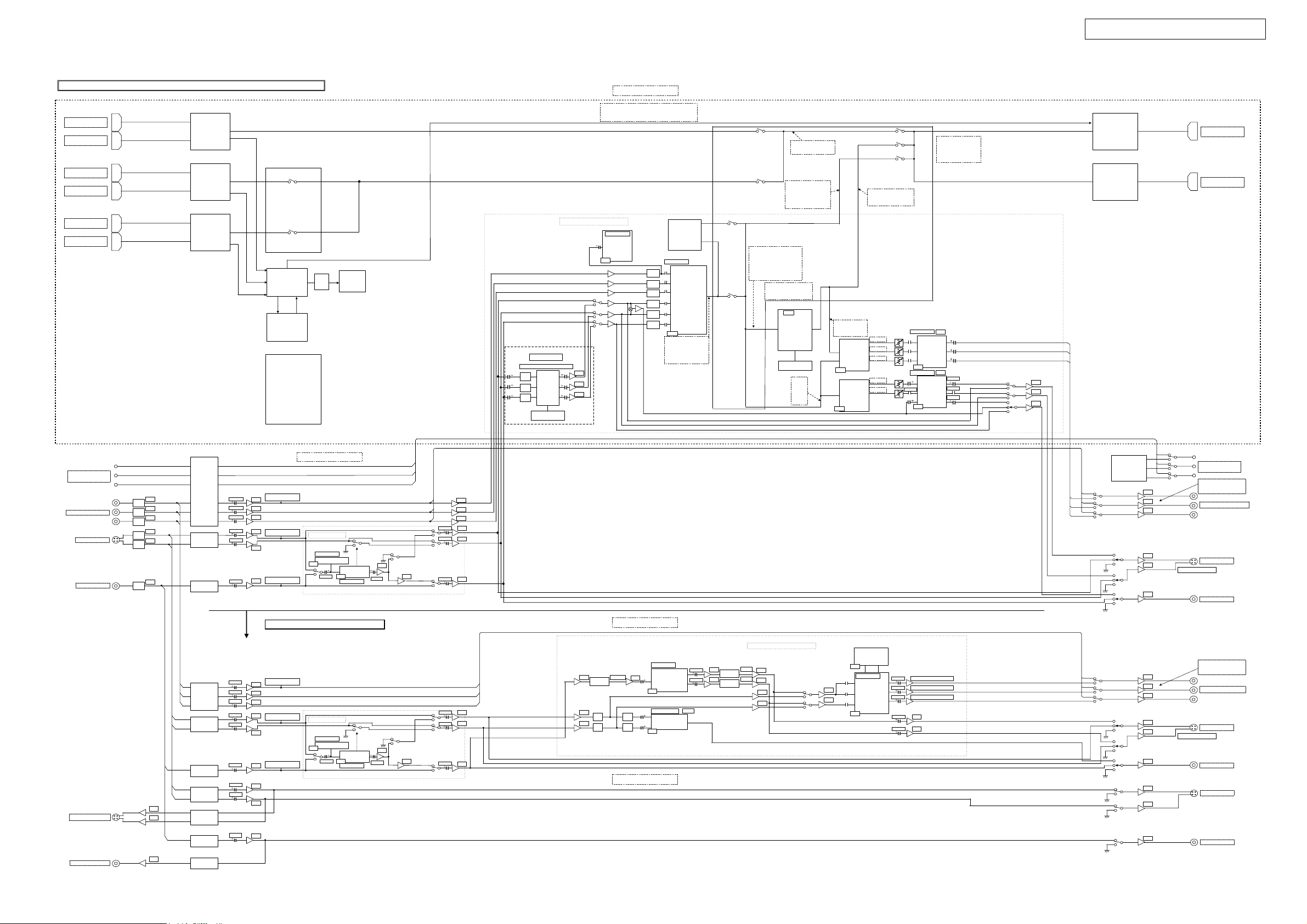
BLOCK DIAGRAMS
AVR-5805/AVC-A1XV-UPGRADE
HDMI
HDMI
HDMI
HDMI
HDMI
DVI
VIDEO BLOCK DIAGRAM
IC203
RECEIVER
SiI9033
IC153
RECEIVER
SiI9033
IC103
RECEIVER
SiI9033
Dock Control
Connector
XM RADIO
XM Supply
The other
unit
IC251
(PLD)
EPM570T144C5N
IC451
Audio signal
selector
EPM570T144C5N
IC457
DSD-PCM
CONVERTER
SM5819A
IC802
VIDEO CPU
M30835FJGP
LVDS
To
Digital
Audio
Block
OPTION
INPUT:2Vpp, OUTPUT:2Vpp
CLAMP
New
CLAMP
OSD
BIAS
FONT ROM
DIGITAL VIDEO UNIT
VIDEO CONVERT BLOCK
INPUT:1Vpp
IC605
FORMAT
DETECTOR
TE8201PF
70℃
0dB
0dB
0dB
ZONE 1
1U-3755-1
-6dB
TT
-6dB
TT
-6dB
TT
-6dB
TT
-6dB
TT
-6dB
TT
OPTION
CONNECTOR
INPUT:1Vpp
INPUT:1Vpp
IC606
VIDEO
DECODER
ADV7403
70℃
SD
ITU-R. BT656 10bit
PS/HD
YCBCR4:2:2 20bit
/RGB 24bit
IC401
FPGA
EP1C4F400C8N
PORT2:
SD
ITU-R. BT656 10bit
PORT1:
PS/HD
YCBCR4:2:2 20bit
YCBCR4:2:2 20bit
/RGB 24bit
SD
ITU-R. BT656 10bit
PS/HD
YCBCR4:2:2 20bit
/RGB 24bit
PS/HD
YCBCR4:2:2 20bit
/RGB 24bit
70℃
IC501
VIDEO
PROCESSOR
FLI2310
64M SDRAM
SD
ONLY
ITU-R.
BT656
10bit
PS/HD
YCBCR
4:2:2 20bit
IC703
VIDEO
ENCODER
ADV7320
70℃
IC753
VIDEO
ENCODER
ADV7320
70℃
PS/HD
YCBCR4:2:2 20bit
/RGB 24bit
DAC D
DAC E
DAC F
DAC E
DAC F
fc:79.6Hz
INPUT:1Vpp
DRIVER WITH
FMS6403
70℃
INPUT:1Vpp
WITH FILTER
BH7868F
70℃
SD
ITU-R. BT656 10bit
PS/HD
YCBCR4:2:2 20bit
RGB 24bit
6dB
IC705
VIDEO
FILTER
6dB
IC755
VIDEO
DRIVER
fc:0.16Hz
fc:159Hz
fc:0.16Hz
IC303
TRANSMITTER
SiI9030
IC353
TRANSMITTER
SiI9030
0dB
0dB
0dB
HDMI
DVI-D
D CONTROL IN
(JAPAN ONLY)
COMPONENT IN
S(Y/C) IN
CVBS IN
S(Y/C) RECOUT
CVBS RECOUT
75
LOAD
75
LOAD
75
LOAD
75
LOAD
75
LOAD
75
LOAD
ANALOG VIDEO
INPUT
-6dB
-6dB
-6dB
-6dB
-6dB
-6dB
0dB
0dB
0dB
SELECTOR
SELECTOR
INPUT
SELECTOR
INPUT
SELECTOR
INPUT
SELECTOR
INPUT
SELECTOR
INPUT
SELECTOR
RECOUT
INHIBIT
INPUT
SELECTOR
RECOUT
INHIBIT
INPUT
fc:0.016Hz
fc:0.016Hz
fc:0.016Hz
fc:0.16Hz
fc:0.16Hz
fc:0.16Hz
fc:0.16Hz
fc:0.16Hz
fc:0.16Hz
fc:0.16Hz
fc:0.16Hz
fc:0.16Hz
fc:0.16Hz
fc:0.16Hz
fc:0.16Hz
SIGNAL DET.
6dB
6dB
6dB
6dB
6dB
6dB
SIGNAL DET.
SIGNAL DET.
OSD BLOCK
INPUT:2Vpp
SYNC. DET.
75℃
fc:0.15Hz
70℃
INPUT:2Vpp
ZONE2/ZONE3 is equal with AVR5805
SIGNAL DET.
6dB
6dB
6dB
6dB
6dB
6dB
6dB
6dB
6dB
SIGNAL DET.
SIGNAL DET.
OSD BLOCK
INPUT:2Vpp
SYNC. DET.
75℃
fc:0.15Hz
70℃
INPUT:2Vpp
OSD
OSD
fc:0.16Hz
fc:0.16Hz
0dB
0dB
0dB
fc:0.16Hz
0dB
fc:0.16Hz
0dB
0dB
0dB
fc:0.16Hz
0dB
ZONE 2
VIDEO CONVERT BLOCK
INPUT:1Vpp
0dB
-12dB
FILTER
fc:0.16Hz
0dB
0dB
fc:0.16Hz
0dB
0dB
fc:0.16Hz
0dB
0dB
-6dB
TT
0dB
-6dB
TT
SEPARATOR
6dB
75℃
INPUT:0.5Vpp
-6dB
-6dB
Y/C MIXER
TT
NJM2274R
TT
85℃
Y/C
TC90A69F
fc:0.16Hz
fc:0.16Hz
12dB
-6dB
0dB
FILTER
0dB
FILTER
6dB
-6dB
6dB
0dB
0dB
0dB
0dB
65℃
INPUT:1Vpp
65℃
PAL
1H DELAY
TA8772AN
CROMA
DECODER
TA1270BF
fc:0.72Hz
㪽㪺㪑㪇㪅㪎㪉㪟㫑
fc:1.59Hz
fc:1.59Hz
fc:0.16Hz
fc:0.16Hz
GAIN ADJ.:11.3dBtyp.
GAIN ADJ.:11.3dBtyp.
GAIN ADJ.:11.3dBtyp.
6dB
6dB
ZONE 3
DC
GENERATOR
0dB
0dB
0dB
0dB
0dB
0dB
0dB
0dB
0dB
0dB
0dB
0dB
0dB
0dB
0dB
D CONTROL OUT
TheoutputMUTEofthe
CONPONENT uses the
function of the CPAMP
COMPONENT OUT
S(Y/C) OUT
S MONI.DET.
TheoutputMUTEofthe
CONPONENT uses the
function of the CPAMP
COMPONENT OUT
S(Y/C) OUT
S MONI.DET.
CVBS OUT
JAPAN ONLY
CVBS OUT
S(Y/C) OUT
CVBS OUT
3

Page 32~34
AVR-5805/AVC-A1XV-UPGRADE
ADJUSTMENT
VIDEO Section
I. MAIN ZONE
1. SETTING
(1) Connect the oscilloscope to the Y-signal and C-signal of
S MONITOR OUT terminal and each terminate at 75
Ohms.
(2) Connect the oscilloscope to the Y-signal, P
B-signal, PR-signal and CR-signal of COMPONENT
C
MONITOR OUT2 terminal and each terminate at 75
Ohms.
※ Use the 75 Ohms resistance must be 1%
(3) DVD test disc : DVDT-S01
(4) COMPONENT VIDEO OUT of DVD player is connected
to COMPONENT IN-5.
2. BEFORE ADJUSTMENT
2.1. Setting the Oscilloscope as below.
(1) PB/CB, PR/CR, C
(a) TIME/DIV : 10μs
(b) VOLT/DIV : 100mV
(Use the probe : x10 )
(2) Y
(a) TIME/DIV : 10μs
(b) VOLT/DIV : 200mV
(Use the probe : x10 )
Power on. Power Supply
U.S.A. & Canada : 120V
Taiwan R.O.C. : 120V
Europe : 230V
Japan : 100V
China & Korea : 220V
2.2. Setup the DVD player and confirmation of the
stators
(1) Set to "INTERLACED" mode at the COMPONENT OUT.
(2) Confirm the DVD player’s out put level is equal as the
item 2.4. in following.
2.3. Preparation
(1) Push [POWER] button with pressing [GAME] and [SUR-
ROUND BACK] buttons.
(2) Confirm "0.0dB" appearing on the FL display.
(3) Turn the FUNCTION knob to select "VCR-1" input.
(4) Push [VIDEO ON/OFF] button twice to select "VIDEO
OFF". (It becomes Adjustment mode.)
(5) Push [OPEN/CLOSE] button of DVD player, then open
the Disc Tray.
Set DVD test disc (DVDT-S01) on the Disc Tray, and
then push [CLOSE] button.
(6) DVD player FL display appear "STOP", push [PLAY] but-
ton to playback DVD.
(7) Push the [DISPLAY] button of remote control of DVD
player unit and then appear the ON-Screen Display (GUI)
on the monitor TV.
(8) Push the [+10] and [2] button, select Title 12 of DVD.
(9) Push the [ENTER] button, playback Title 12.
(color bar 75%)
B-signal and
調整
ビデオセクション
I.MAINZONE
1. セッティング手順
(1) セットの SMONITOROUT 端子から Y 信号と C 信号を
それぞれオシロスコープ(終端抵抗:75Ω)に接続し
ます。
(2) セットの COMPONENTMONITOROUT2 の端子(Y,
B/CB,PR/CR)をそれぞれオシロスコープ(終端抵抗:
P
75Ω)に接続します。
※ 75Ω 抵抗は 1%品を使用する事。
(3) DVD テストディスク:DVDT-S01 を用意します。
(4) DVD プレーヤーの COMPONENTVIDEOOUT を
COMPONENTIN-5 に接続します。
2. 調整のまえに
2.1. オシロスコープを下記に設定
(1) PB/CB,PR/CR,C
(a) TIME/DIV : 10μs
(b) VOLT/DIV : 100mV
(プローブ x10 使用)
(2) Y
(a) TIME/DIV : 10μs
(b) VOLT/DIV : 200mV
(プローブ x10 使用)
電源電圧 : 100V
2.2. DVD プレーヤの設定と確認
(1) COMPONENTOUT の設定を " インターレース " にしま
す。
(2) DVD プレーヤーの出力が以下 2.4. に合っていることを
確認します。
2.3. 準備手順
(1) セットの AC コードをコンセントへ挿入し、「GAME」
と「SURROUNDBACK」ボタンを押しながらセットの電
源を "ON" にします。
(2) FL 表示右上の VOL 表示が "0.0dB" になっていることを
確認します。
(3) FUNCTION ノブを回し、入力を "VCR-1" に切り替えます。
(4) 「VIDEOON/OFF」ボタンを 2 回押し、"VIDEOOFF" に
します。(調整モードになります)
(5) DVD プレーヤーの「OPEN/CLOSE」ボタンを押しトレ
イを開き、トレイ上に DVD テストディスク(DVDT-
S01)をセット後、「CLOSE」ボタンを押します。
(6) DVD プレーヤーの表示管上に "STOP" が表示されてか
ら、「PLAY」ボタンを押し、ディスクを再生します。
(7) DVD プレーヤーのリモコンの「DISPLAY」ボタンを押
しグラフィカル・ユーザー・インターフェイス (GUI) 画
面を出します。
(8) 番号ボタンの「 +10 」 , 「 2 」ボタンを押し、Title12 を選択
します。
(9) 「ENTER」ボタンを押し、Title12 を再生します。
(75%カラーバー信号)
4
AVR-5805/AVC-A1XV-UPGRADE
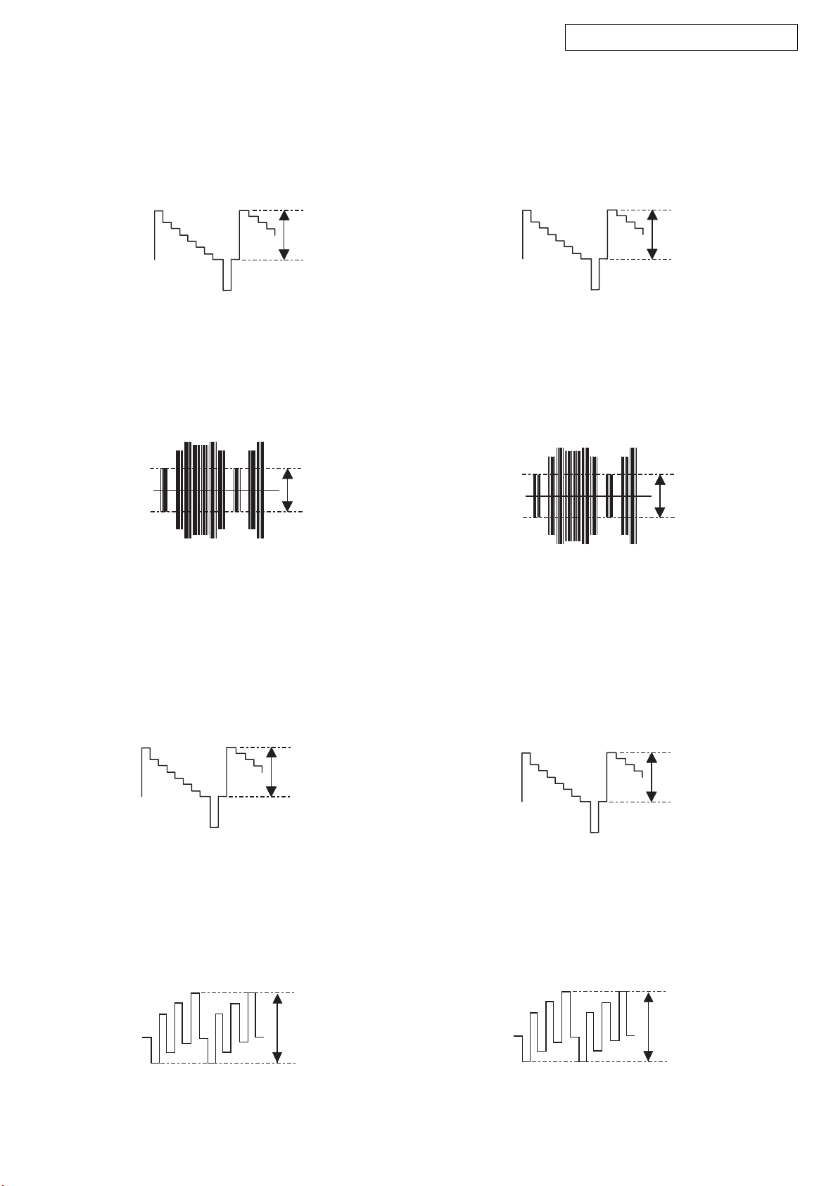
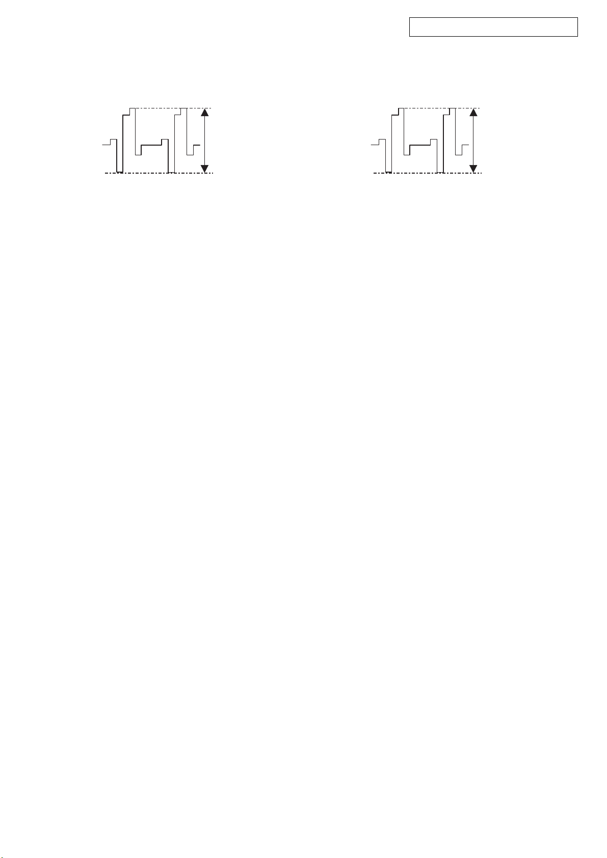
2.4. Procedure
(1) Adjust the signal of S MONITOR OUT by the wave of os-
cilloscope.
(a) Target, Y-signal
Point : 1U-3755-1 VR751
Adjustment Value : 714 ± 14mV
Waveform
Y
Y-signal of S MONITOR OUT
(b) Target, C-signal
Point : 1U-3755-1 VR752
Adjustment Value : 286 ± 5mV
Waveform
2.4. 手順
(1) セットの SMONITOROUT の信号レベルをオシロスコー
プ上の波高値で調整します。
(a) Y 信号レベル
調整個所 : 1U-3755-1VR751
調整値 : 714 ± 14mV
波形
Y
SMONITOROUT の Y 信号レベル
(b) C 信号レベル
調整個所 : 1U-3755-1VR752
調整値 : 286 ± 5mV
波形
C
C-signal of S-MONITOR
(2) Adjust the signal of COMPONENT OUT by the wave of
oscilloscope.
(a) Target, Y-signal
Point : 1U-3755-1 VR701
Adjustment Value : 714 ± 14mV
Waveform
Y
Y-signal COMPONENT OUT
C
SMONITOR の C 信号レベル
(2) COMPONENTOUTの信号レベルをオシロスコープ上の
波高値で調整します。
(a) Y 信号レベル
調整個所 : 1U-3755-1VR701
調整値 : 714 ± 14mV
波形
Y
COMPONENTOUT の Y 信号レベル
(b) Target, P
Point : 1U-3755-1 VR702
Adjustment Value : *525 ± 10mV
Waveform
B/CB-signal
PB/CB
PB/CB-signal COMPONENT OUT
B/CB 信号レベル
(b) P
調整個所 : 1U-3755-1VR702
調整値 : 525 ± 10mV
波形
PB/CB
COMPONENTOUT の PB/CB 信号レベル
5
AVR-5805/AVC-A1XV-UPGRADE
(c) Target, PR/CR-signal
Point : 1U-3755-1 VR703
Adjustment Value : *525 ± 10mV
Waveform
PR/CR
PR/CR-signal COMPONENT OUT
* : 486 ± 10mV for U.S.A. & Canada model
(c) PR/CR 信号レベル
調整個所 : 1U-3755-1VR703
調整値 : 525 ± 10mV
波形
PR/CR
COMPONENTOUT の PR/CR 信号レベル
6
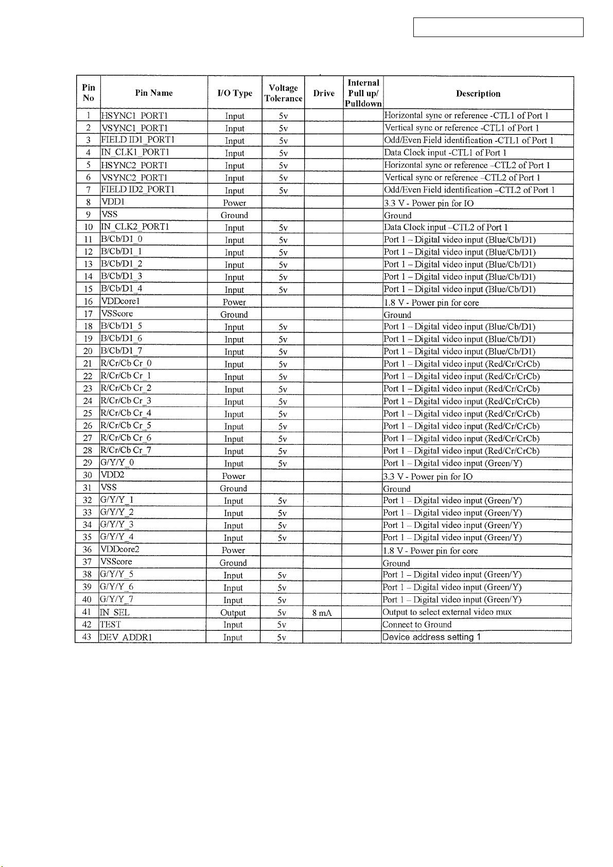
Page 37~74
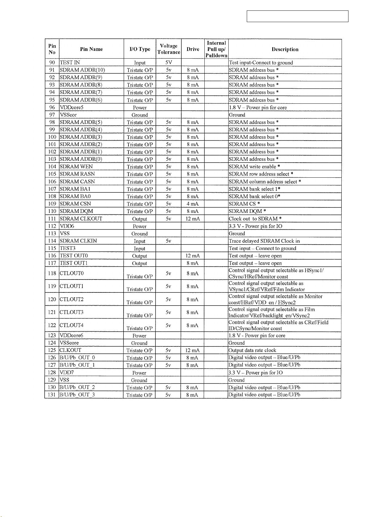
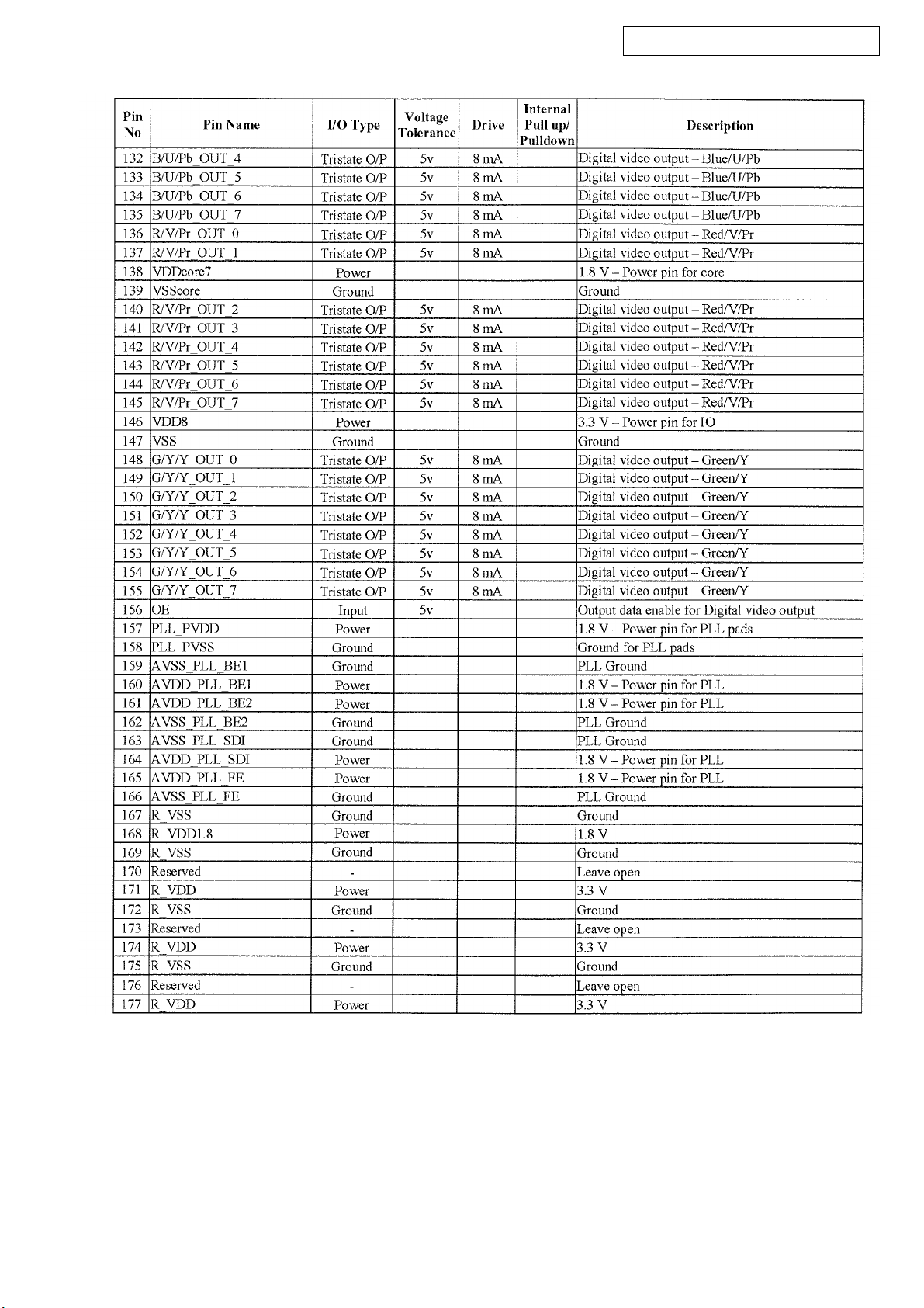
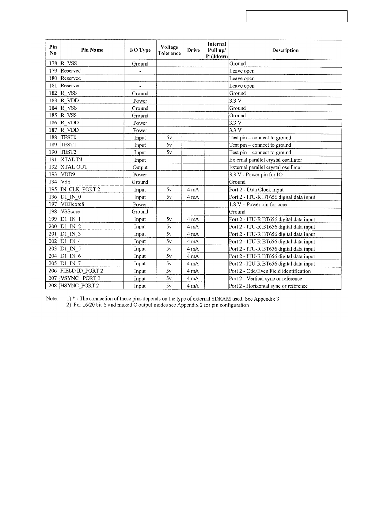
SEMICONDUCTORS (for 00D1U-3755A D.VIDEO P.W.B.)
Only major semiconductors are shown, general semiconductors etc. are omitted to list.
主な半導体を記載しています。汎用の半導体は記載を省略しています。
IC’s
FLI2310-LF-CF (IC501)
AVR-5805/AVC-A1XV-UPGRADE
7
Terminal Function
AVR-5805/AVC-A1XV-UPGRADE
8
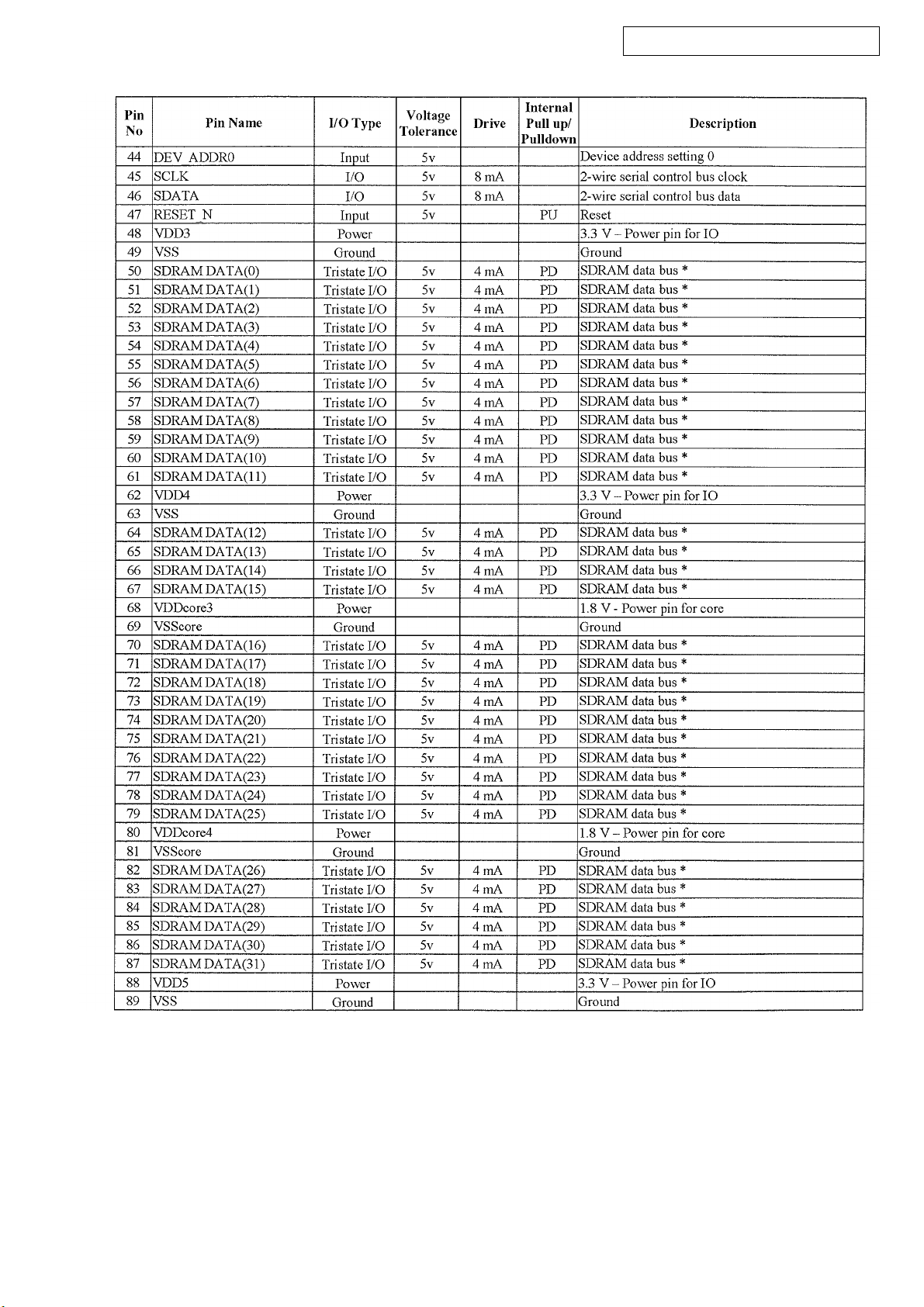
AVR-5805/AVC-A1XV-UPGRADE
9
AVR-5805/AVC-A1XV-UPGRADE
10
AVR-5805/AVC-A1XV-UPGRADE
11
AVR-5805/AVC-A1XV-UPGRADE
12
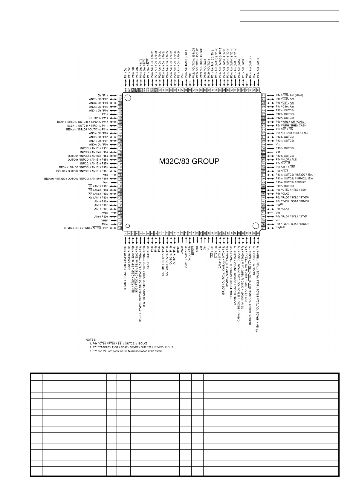
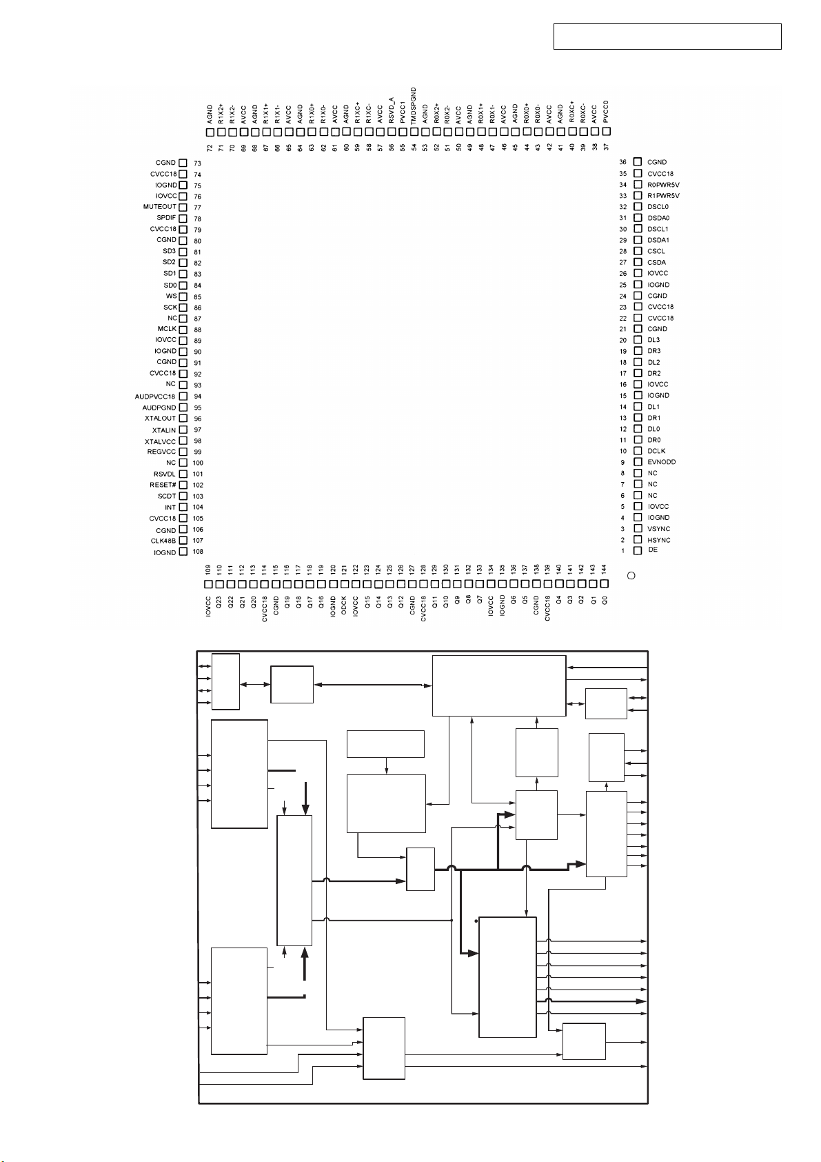
M30835FJGP (IC802)
AVR-5805/AVC-A1XV-UPGRADE
M30835FJGP Terminal Function
Pin Pin name Symbol I/O Type Det Op(Int.) Op(Ext.) Res stop Function
1 P96/TXD4 (GIVO) O C - - (-) Z O/L NC(VIDEO-GUI Communication Control terminal)
2 P95/CLK4 (CLK GIVO) O C - - (-) Z O/L NC(VIDEO-GUI Communication Control terminal)
3 P94/CTS4 (REQ GOVI) O C - - (-) Z O/L NC(VIDEO-GUI Communication Control terminal)
4 P93/CTS3 Z1VCONV.B O C - - Ed Z O/L MAIN CVBS Routing control(convert/through)(TC4052)
5 P92/TXD3/SDA3 HDMI SDA I/O C - - - Z O/L HDMI T/R/EDIT(E2PROM)Control terminal
6 P91/RXD3/SCL3 HDMI SCL I/O C - - - Z O/L HDMI T/R/EDIT(E2PROM)Control terminal
7 P90/CLK3 Z1VCONV.A O C - - Ed Z O/L MAIN CVBS Routing control(convert/through)(TC4052)
8 P146 Z1SCONV.B O C - - Ed Z O/L MAIN S Routing control(convert/through)(TC4052)
9 P145 Z1SCONV.A O C - - Ed Z O/L MAIN S Routing control(convert/through)(TC4052)
10 P144 CV/MIX O C - - - Z O/L Y/C MIX selection control(convert/analog MIX )(BH7868)
11 P143 (XM RST) O C - - (-) Z O/L (XM RADIO terminal for control)
12 P142 (XM COMMAND) O C - - (-) Z O/L (XM RADIO terminal for control)
13 P141 (XM POWER) O C - - (-) Z O/L (XM RADIO power on/off switching(ONÅFH))
14 P140 (XMDACMDI) O C - - (-) Z O/L (DAC control terminal for XM(AK4385ET))
15 BYTE BYTE - - - - - - - GND(Ext. data bus bit width switching, 16bit="L")
16 CNVss CNVSS I - - - Ed - - "Single-chip/Micro-processor mode switching (Normal single-chip:L, Rewrite boot
program start:H input set)"
13
AVR-5805/AVC-A1XV-UPGRADE
Pin Pin name Symbol I/O Type Det Op(Int.) Op(Ext.) Res stop Function
17 P87/XCIN (XMDACRST) O C - - (-) Z O/L (DAC control terminal for XM(AK4385ET))
18 P86/XCOUT (XMDACMUTE) O C - - (-) Z O/L (DAC output MUTE control terminal for XM )
19 RESET RESET I - Lv - Eu L I Reset input(Reset:"L")
20 XOUT X2 O - - - - - - Clock output
21 VSS VSS - - - - - - - GND
22 XIN X1 I - - - - - I Clock input
23VCC VCC ---- ---+3.3V
24 P85/NMI _NMI I - - - - - - Not used(Fixed:"H")
25 P84/INT2 (REMOTE) I 26 P83/INT1 V.B.DOWN I 27 P82/INT0 (REQ XM) O C - - (-) Z O/L (XM RADIO terminal for control)
28 P81/ (XMDACCS) O C - - (-) Z O/L (DAC control terminal for XM(AK4385ET))
29 P80/ISRXD0 (RXD MIXMO) O C - - (-) Z O/L (XM RADIO terminal for control)
30 P77/ISCLK0 (XMDACMC) O C - - (-) Z O/L (DAC control terminal for XM(AK4385ET))
31 P76/ISTXD0 (TXD MOXMI) O C - - (-) Z O/L (XM RADIO terminal for control)
32 P75/ISRXD1 (RXD iPod) O C - - (-) Z O/L (IPOD communication control terminal)
33 P74/ISCLK1 (iPOD CON DET) O C - - (-) Z O/L (IPOD detect terminal("L": DETECT)
34 P73/CTS2/ISTXD1 (TXD_iPod) O C - - (-) Z O/L (IPOD communication control terminal)
35 P72/CLK2 CLK VIMO I - Lv - - Z O/L MAIN-VIDEO communication control terminal
36 P71/RXD2/ VIMO I - Lv - Eu Z O/L MAIN-VIDEO communication control terminal
37 P70/TXD2/ VOMI O N - - Eu Z O/L MAIN-VIDEO communication control terminal
38 P67/TXD1 FRONT TxD O C - - - Z O/L Data transfer terminal to outside(MAKER BOOT)
39VCC VCC ---- ---+3.3V
40 P66/RXD1 FRONT RxD I - Lv - - Z O/L Data reception terminal from Ext.(MAKER BOOT)
41 VSS VSS - - - - - - - GND
42 P65/CLK1 REQ VOMI O C - - - Z O/L MAIN-VIDEO communication control terminal
43 P64/CTS1 VSEL0 O C - - - Z O/L BUS SW(FPGA)switching control terminal
44 P63/TXD0 ZONE1 SDA I/O C - - - Z O/L VIDEO I2C control terminal
45 P62/RXD0 ZONE1 SCL I/O C - - - Z O/L VIDEO I2C control terminal
46 P61/CLK0 Z2 VSIG DET I - Lv - Eu Z O/L ZONE2 VIDEO IN signal detect input(signal input:"H")
47 P60/CTS0 Z1 VSIG DET I - Lv - Eu Z O/L MAIN ZONE VIDEO IN signal detect input(signal input:"H")
48 P137 Z1 OSD RST O C - - - Z O/L MAIN OSD control terminal(M35015)
49 P136/ISCLK2 Z1 OSD CLK O C - - - Z O/L MAIN OSD control terminal(M35015)
50 P135/ISRXD2 Z1 OSD STB O C - - - Z O/L MAIN OSD control terminal(M35015)
51 P134/ISTXD2 Z1 OSD DATA O C - - - Z O/L MAIN OSD control terminal(M35015)
52 P57 ZONE2 SDA I/O C - - - Z O/L ZONE2 VIDEO I2C control terminal(TA1270/TC90A69F)
53 P56 ZONE2 SCL I/O C - - - Z O/L ZONE2 VIDEO I2C control terminal(TA1270/TC90A69F)
54 P55/EPM FRASH EPM I - - - Ed Z I Rewrite boot program start: "L" Input setting
55 P54 Z1 SMONIDET I - Lv - Eu Z O/L S MONITER connection detect input for MNAIN ZONE (Connected:"L")
56 P133 Z2 S SIG DET I - Lv - Eu Z O/L MAIN ZONE S signal detect input(Connecte:"H")
57 VSS VSS - - - - - - - GND
58 P132 Z1 S SIG DET I - Lv - Eu Z O/L MAIN ZONE S signal detect input(Connecte:"H")
59VCC VCC ---- ---+3.3V
60 P131 Z2 SMONIDET I - Lv - Eu Z O/L S MONITER connection detect input for ZONE2(Connected:"L")
61 P130 SV EXP OE O C - - Ed Z O/L Control terminal switching for COMPONENT section, Expander control(BU4094B)
62 P53 SV EXP STB O C - - - Z O/L Control terminal switching for COMPONENT section, Expander control
63 P52 SV EXP DATA O C - - - Z O/L Control terminal switching for COMPONENT section, Expander control(BU4094B)
64 P51 SV EXP CLK O C - - - Z O/L Control terminal switching for COMPONENT section, Expander control
65 P50/CE FRASH CE I - - - Ed Z I Rewrite boot program start:H input set
66 P127 C EXP OE O C - - Ed Z O/L Control terminal switching for COMPONENT section, Expander control(BU4094B)
67 P126 C EXP STB O C - - - Z O/L Control terminal switching for COMPONENT section, Expander control(BU4094B)
68 P125 C EXP DATA O C - - - Z O/L Control terminal switching for COMPONENT section, Expander control(BU4094B)
69 P47/CS0/A23 C EXP CLK O C - - - Z O/L Control terminal switching for COMPONENT section, Expander control(BU4094B)
70 P46/CS1/A22 COMP SDET1 I - Lv - Eu Z O/L COMPONENT IN signal detect input for MAIN ZONE
71 P45/CS2/A21 COMP SDET2 I - Lv - Eu Z O/L COMPONENT IN signal detect input for ZONE2
72 P44/CS3/A20 Z2 OSD RST O C - - - Z O/L ZONE2 OSD control terminal(M35015)
73 P43/A19 Z2 OSD STB O C - - - Z O/L ZONE2 OSD control terminal(M35015)
74VCC VCC ---- ---+3.3V
75 P42/A18 Z2 OSD CLK O C - - - Z O/L ZONE2 OSD control terminal(M35015)
76 VSS VSS - - - - - - - GND
77 P41/A17 Z2 OSD DATA O C - - - Z O/L ZONE2 OSD control terminal(M35015)
78 P40/A16 Z2 SYNC DET I - Lv - Eu Z O/L Synchronous detect input for ZONE2(Ext.Synchronous:H)
79 P37/D15 Z1 SYNC DET I - Lv - Eu Z O/L Synchronous detect input for MAIN(Ext.Synchronous:H)
80 P36/D14 OSDOUTSEL O C - - Ed Z O/L MAIN OSD Routing control
81 P35/D13 OSDRST O C - - - Z O/L NEW OSD control terminal(LC74731W)
82 P34/D12 OSDCLK O C - - - Z O/L NEW OSD control terminal(LC74731W)
83 P33/A11 OSDSIN O C - - - Z O/L NEW OSD control terminal(LC74731W)
84 P32/D10 OSDCS O C - - - Z O/L NEW OSD control terminal(LC74731W)
85 P31/D9 OSDMUTE O C - - - Z O/L NEW OSD control terminal(LC74731W)
86 P124 V/Y SEL O C - - Ed Z O/L MAIN NEW OSD control of input signal selection(S/CVBS)(TC4053)
87 P123 Y/C SEL O C - - Ed Z O/L Croma Decoder SELECT for ZONE2
88 P122/ISRXD3 VÇéCONFIG O C - - - Z O/L FPGA rewrite control terminal
89 P121/ISCLK3 V DATAOUT O C - - - Z O/L FPGA rewrite control terminal
90 P120/ISTXD3 V ASDI O C - - - Z O/L FPGA rewrite control terminal
91VCC VCC ---- ---+3.3V
92 P30/D8 VnCS O C - - - Z O/L FPGA rewrite control terminal
93 VSS VSS - - - - - - - GND
E↑&L
E↓&L
- Ed Z I Remote control signal input(TEST:usually unused thing)
- Eu Z I Power down detect (Power down: L)
14
AVR-5805/AVC-A1XV-UPGRADE
Pin Pin name Symbol I/O Type Det Op(Int.) Op(Ext.) Res stop Function
94 P27/AN27/D7 VDCLK O C - - - Z O/L FPGA rewrite control terminal
95 P26/AN26/D6 VCONF_DONE I - Lv - - Z O/L FPGA rewrite control terminal
96 P25/AN25/D5 VCPUASON O C - - - Z O/L
97 P24/AN24/D4 VnCE O C - - - Z O/L FPGA rewrite control terminal
98 P23/AN23/D3 VSEL5 O C - - - Z O/L BUS SW(FPGA) switching control terminal
99 P22/AN22/D2 VSEL4 O C - - - Z O/L BUS SW(FPGA) switching control terminal
100 P21/AN21/D1 VSEL3 O C - - - Z O/L BUS SW(FPGA) switching control terminal
101 P20/AN20/D0 VSEL2 O C - - - Z O/L BUS SW(FPGA) switching control terminal
102 P17/INT5/D15 VSEL1 O C - - - Z O/L BUS SW(FPGA) switching control terminal
103 P16/INT4/D14 ACK VIMO I 104 P15/INT3/D13 HDMIVS. I 105 P14/D12 TDO O C - - - Z O/L JTAG terminal for rewriting
106 P13/D11 FPGATDI I - Lv - - Z O/L JTAG terminal for rewriting
107 P12/D10 TMS O C - - - Z O/L JTAG terminal for rewriting
108 P11/D9 TCK O C - - - Z O/L JTAG terminal for rewriting
109 P10/D8 HDMI IN1 O C - - Ed Z O/L HDMI input selection control terminal
110 P07/AN07/D7 HDMI IN2 O C - - Ed Z O/L HDMI input selection control terminal
111 P06/AN06/D6 HDMI IN3 O C - - Ed Z O/L HDMI input selection control terminal
112 P05/AN05/D5 HDMI R RST1 O C - - Ed Z O/L Reset for HDMI RECEIVER(Si I9031)(DVI/HDMI1)
113 P04/AN04/D4 HDMI R RST2 O C - - Ed Z O/L Reset for HDMI RECEIVER(Si I9031)(HDMI2/3)
114 P114 HDMI R RST3 O C - - Ed Z O/L Reset for HDMI RECEIVER(Si I9031)(HDMI4/5)
115 P113 SCDT I - Lv - - Z O/L HDMI RECEIVER(Si I9031) SCDT output detection
116 P112/ INT I - Lv - - Z O/L HDMI RECEIVER(Si I9031) INT output detection
117 P111/ WPCPU1 O C - - - Z O/L WRITE PROTECT terminalfor HDMI IN EDIT(24LC02)
118 P110/ WPCPU2 O C - - - Z O/L WRITE PROTECT terminalfor HDMI IN EDIT(24LC02)
119 P03/AN03/D3 PRMVCPU1 O C - - - Z O/L HDMI IN Terminal, HP DET control terminal
120 P02/AN02/D2 PRMVCPU2 O C - - - Z O/L HDMI IN Terminal, HP DET control terminal
121 P01/AN01/D1 AUDIO1 O C - - - Z O/L HDMI AUDIO selection
122 P00/AN00/D0 AUDIO2 O C - - - Z O/L HDMI AUDIO selection
123 P157/AN157 AUDIO3 O C - - - Z O/L HDMI AUDIO selection
124 P156/AN156 HDMI T RST1 O C - - Ed Z O/L Reset for HDMI TRANSMITTER (Si I9030)
125 P155/AN155 HDMI SENS1 I 126 P154/AN154 HDMI T RST2 O C - - Ed Z O/L Reset for HDMI TRANSMITTER (Si I9030)
127 P153/AN153 HDMI SENS2 I 128 P152/AN152/ CFSEL0 O C - - - Z O/L Image resolution selection control terminal
129 P151/AN151/ CFSEL1 O C - - - Z O/L Image resolution selection control terminal
130 VSS VSS - - - - - - - GND
131 P150/AN150/ VIDEO POWER O C - - Ed Z O/L VIDEO POWER control terminal(ON:"H")
132 VCC VCC - - - - - - - +3.3V
133 P107/AN7 IP RST O C - - Ed Z O/L Reset for IP CONVERTER(FLI2310)
134 P106/AN6 TE RST O C - - Ed Z O/L Reset for COMPONENT FORMAT DETECTOR (TE8200PF)
135 P105/AN5 VD RSTZ1 O C - - Ed Z O/L Reset for VIDEO DECODER(ADV7403)
136 P104/AN4 Z1CERST O C - - Ed Z O/L Reset for COMPONENT ENCODER(ADV7320)
137 P103/AN3 Z1SVERST O C - - Ed Z O/L Reset for S/CVBS ENCODER(ADV7320)
138 P102/AN2 (G BDOWN) O C - - (-) Z O/L NC(VIDEO-GUI communication control terminal)
139 P101/AN1 (RST G) O C - - (-) Z O/L NC(VIDEO-GUI communication control terminal)
140 AVSS AVSS - - - - - - - Analog GND
141 P100/AN0 (ACK GIVO) O C - - (-) Z O/L NC(VIDEO-GUI communication control terminal)
142 VREF VREF - - - - - - - Standard power input +3.3V
143 AVCC AVCC - - - - - - - Analog power +3.3V
144 P97/ADTRG/RXD4 (GOVI) O C - - (-) Z O/L NC(VIDEO-GUI communication control terminal)
E↑&L
E↓&L
E↓&L
E↓&L
- - Z O/L MAIN-VIDEO communication Control terminal
- - Z O/L HDMI V SYNC input terminal for count
- - Z O/L HDMI IN signal detect input
- - Z O/L HDMI IN signal detect input
Rewrite for FPGAROM ON=L ※ Initial setting, V.POWER OFF=H
15
SiI9033CTU (IC103, 153, 203)
AVR-5805/AVC-A1XV-UPGRADE
Block Diagram
DSDA0
DSCL0
DSDA1
DSCL1
R1XC±
R1X0±
R1X1±
R1X2±
R0XC±
R0X0±
R0X1±
R0X2±
R0PWR5V
R1PWR5V
Port
MUX
PanelLink
TM
TMDS
Digital
Core
PanelLink
TM
TMDS
Digital
Core
Slave
HS,VS,
DE
HS,VS,
DE
2
C
I
HDCP
Embedded Keys
24-Bit
Date
HDCP &
Repeater
Decryption
Engine
XOR
Control Signais
Port
Detect
Mask
M
Port
X
U
24-Bit
Date
24-Bit Encrypted
Pixel Data
Registers
----------------
Configuration
Logic Block
24-Bit
Decrypted
Pixel Data
Video Color
Spade
Converter
Up/Down
Sampling
Aux
Data
HDMI
Mode
Control
Auto A/V
Exception
Handling
2
C
I
Slave
MCLK
Men
Audio
Data
Decode
RESET#
INT
CSDA
CSCL
MCLKOUT
XTALIN
XTALOUT
SCK
WS
SD[3:0]
SPDIF
DCLK
DL[3:0]
DR[3:0]
EVNODO
DE
HSYNC
VSYNC
ODCK
Q[23:0]
CLK48B
MUTEOUT
SCDT
16
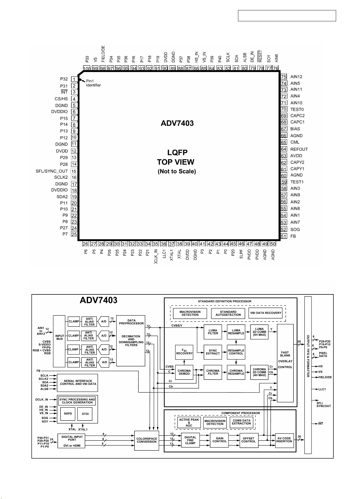
ADV7403BSTZ-110 (IC606)
AVR-5805/AVC-A1XV-UPGRADE
Block Diagram
17
Pin description
AVR-5805/AVC-A1XV-UPGRADE
18

K4S643232H-UC60 (IC505)
V
DQ0
DDQ
V
DQ1
DQ2
SSQ
V
DQ3
DQ4
V
DDQ
DQ5
DQ6
V
SSQ
DQ7
N.C
V
DQM0
WE
CAS
RAS
CS
N.C
BA0
BA1
A10/AP
DQM2
V
N.C
DQ16
V
SSQ
DQ17
DQ18
DDQ
V
DQ19
DQ20
SSQ
V
DQ21
DQ22
DDQ
V
DQ23
V
AVR-5805/AVC-A1XV-UPGRADE
DD
1
2
3
4
5
6
7
8
9
10
11
12
13
14
DD
15
16
17
18
19
20
21
22
23
24
25
A0
26
A1
27
A2
28
29
DD
30
31
32
33
34
35
36
37
38
39
40
41
42
43
DD
V
SS
86
DQ15
85
SSQ
V
84
DQ14
83
DQ13
82
DDQ
V
81
DQ12
80
DQ11
79
SSQ
V
78
DQ10
77
DQ9
76
DDQ
V
75
DQ8
74
N.C
73
SS
V
72
DQM1
71
N.C
70
N.C
69
CLK
68
CKE
67
A9
66
A8
65
A7
64
A6
63
A5
62
A4
61
A3
60
DQM3
59
V
SS
58
N.C
57
DQ31
56
DDQ
V
55
DQ30
54
DQ29
53
SSQ
V
52
DQ28
51
DQ27
50
DDQ
V
49
DQ26
48
DQ25
47
SSQ
V
46
DQ24
45
V
SS
44
Block Diagram
LWE
LDQM
DQi
Output BufferI/O Control
Sense AMP
512K x 32
Data Input Register
512K x 32
Row Decoder Col. Buffer
512K x 32
512K x 32
Column Decoder
Latency & Burst Length
Programming Register
LCAS LWCBR
Timing Register
RAS CAS WE DQM
Row Buffer
Refresh Counter
Bank Select
LCBR
LRAS
Address Register
CLK
ADD
19
LRAS LCBR LWE
CLK CKE CS
LCKE

Pin description
Pin Name Input Function
CLK System clock Active on the positive going edge to sample all inputs.
CS
CKE Clock enable
0
~ A
10
A
BA0,1 Bank select address
RAS
CAS
WE
DQM0 ~ 3 Data input/output mask
0
~
31
DQ
V
DD/VSS
V
DDQ/VSSQ
NC No Connection This pin is recommended to be left No connection on the device.
AVR-5805/AVC-A1XV-UPGRADE
Chip select
Address
Row address strobe
Column address strobe
Write enable
Data input/output Data inputs/outputs are multiplexed on the same pins.
Power supply/ground Power and ground for the input buffers and the core logic.
Data output power/ground
Disables or enables device operation by masking or enabling all inputs except
CLK, CKE and DQM.
Masks system clock to freeze operation from the next clock cycle.
CKE should be enabled at least one cycle prior to new command.
Disables input buffers for power down mode.
Row/column addresses are multiplexed on the same pins.
0
Row address : RA
~ RA10, Column address : CA0 ~ CA
Selects bank to be activated during row address latch time.
Selects bank for read/write during column address latch time.
Latches row addresses on the positive going edge of the CLK with RAS
Enables row access & precharge.
Latches column addresses on the positive going edge of the CLK with CAS
Enables column access.
Enables write operation and row precharge.
Latches data in starting from CAS
Makes data output Hi-Z, t
, WE active.
SHZ
after the clock and masks the output.
Blocks data input when DQM active.
Isolated power supply and ground for the output buffers to provide improved noise
immunity.
7
low.
low.
20

SiI9030CTU-7 (IC303, 353)
AVR-5805/AVC-A1XV-UPGRADE
Functional Block Diagram
21

ADV7320 (IC703, 753)
AVR-5805/AVC-A1XV-UPGRADE
22

SM5819A (IC457)
Block Diagram
AVR-5805/AVC-A1XV-UPGRADE
23

Pin description
AVR-5805/AVC-A1XV-UPGRADE
24

BH7868FS (IC755)
AVR-5805/AVC-A1XV-UPGRADE
TC74VHC244FT (IC804)
TC74VHCT244AFT (IC805, 806, 812) SN65LVDS050PWR (IC809)
1B
1A
1R
RE
2R
2A
2B
GND
(TOP VIEW)
16
1
2
15
3
14
4
13
5
12
6
11
7
10
8
9
V
1D
1Y
1Z
DE
2Z
2Y
2D
CC
1D
DE
2D
1R
RE
2R
15
12
25
14
1Y
13
1Z
10
9
3
4
5
2Y
11
2Z
2
1A
1
1B
6
2A
7
2B

AVR-5805/AVC-A1XV-UPGRADE
100k
RCH1
100k
RCH3
–
+
–
+
0.5pF
UVLO
3SCLIN
4300-2 BD
CONNECT CONNECT
STOP BIT AND BUS IDLE
4
4
GND
20pF
RD
S
QB
0.5µA
0.55V
CC
/
0.45V
CC
–
+
–
+
0.55V
CC2
/
0.45V
CC2
2mA
95µs
DELAY
BACKPLANE-TO-CARD
CONNECTION
CONNECTCONNECT
2 SCLOUT
6SDAIN
8V
CC
BACKPLANE-TO-CARD
CONNECTION
CONNECT
CONNECT
7 SDAOUT
1 V
CC2
5 ACC
1V
PRECHARGE
100k
RCH2
100k
RCH4
CONNECT
SLEW RATE
DECTECTOR
2mA
SLEW RATE
DECTECTOR
2mA
SLEW RATE
DECTECTOR
ACC
ACC
2mA
SLEW RATE
DECTECTOR
E
*
TOP VIEW
TC4053BFT (IC601) TC4052BFT (IC756, 757)
SN65LVDS2DBVR (IC811)
V
CC
GND
1
2
3
A
R
5
4
B
LTC4300-2CMS8 (IC807)
CC2
SCLOUT
SCLIN
GND
1
*
2
3
4
8
V
CC
SDAOUT
7
SDAIN
6
READY/ACC
5
NABLE/V
Blocl Diagram
ዴȐǹȷȐȃȕǡƱțȃȈǹȯȃȗȷdzȳȈȭȸȩ
2
26

BR24L02F-WE2 (IC101, 102, 151, 152, 201, 202)
AVR-5805/AVC-A1XV-UPGRADE
Pinconfiguration
V
CC
WP
SCLA2SDA
1234
A0
A1
Block diagagram
1
A0
8bit
A1 2
A2 3
GND 4
Address
decoder
High voltage generator Vcc level detect
5678
GND
8bits
Control logic
Pin name
*1 An open drain output requires a pull-up resistor.
2kbit EEPROM array
Slave word
address register
STOPSTART
Pin name
V
CC
GND
A0, A1, A2
SCL
SDA
WP
ACK
IN / OUT
8bit
Data
register
I/O
Power supply
Ground (0V)
IN
Slave address set
Serial clock input
IN
Slave and word address,
serial data input, serial data output
IN
Write protect input
VCC8
WP7
6SCL
SDA5
Function
*1
LTC1694CS5 (IC801, 803)
TOP VIEW
VCC1
GND 2
NC 3
BLOCK DIAGRA
5 SMBus1
4 SMBus2
M
V
CC
1
2.2mA
SMBus1
5
GND
2
SMBus2
4
0.65V
V
REF
+
VOLTAGE
PI N FUNCTIONS
VCC(Pin 1): Power Supply Input. V
to 6V and requires a 0.1
Supply current is typically 45
lines are inactive (SCL and SDA are a logic high level).
GND (Pin 2):Ground.
SLEW RATE
DETECTOR
COMP
-
CHANNEL ONE
CONTROL
LOGIC
CHANNEL TWO
(DUPLICATE OF CHANNEL ONE)
μ
F bypass capacitor to GND.
μ
A when the SMBus or I2C
can range from 2.7V
CC
NC (Pin 3):No Connection.
SMBus2 (Pin 4):Active Pull-Up for SMBus.
SMBus1 (Pin 5):Active Pull-Up for SMBus.
SN65LVDS1DBVR (IC456) LM1117MPX-1.8 (IC104, 154, 204, 302, 352, 502)
V
CC
GND
1
5
D
2
3
4
Z
Y
27

Page 96, 97
PRINTED WIRING BOARDS
1U-3755A D. VIDEO P.W.B. UNIT
AVR-5805/AVC-A1XV-UPGRADE
28
COMPONENT SIDE (1/2)

AVR-5805/AVC-A1XV-UPGRADE
29
COMPONENT SIDE (2/2)

AVR-5805/AVC-A1XV-UPGRADE
30
FOIL SIDE (1/2)

AVR-5805/AVC-A1XV-UPGRADE
31
FOIL SIDE (2/2)

AVR-5805/AVC-A1XV-UPGRADE
Page 150~158
PARTS LIST OF P.W.B. UNIT ASS’Y
*本表に記載されている部品は、補修用部品のため製品に使用している部品とは一部、形状、寸法などが異なる場合があります。
* The parts listed below are for maintenance only, might differ from the parts used in the unit in appearances or dimensions.
*"nsp" 印の部品は常時在庫していませんので供給に長時間を要することがあります。場合によっては、供給をお断りする場合があります。
* Part indicated with the mark “nsp” are not always in stock and possibly to take a long period of time for supplying, or in some case supplying of part may be refused.
00D1U-3755A D.VIDEO P.W.B. UNIT ASS'Y
Ref. No. nsp Part No. Part Name Remarks Q'ty New
SEMICONDUCTORS GROUP
IC101,102 00D 262 3416 901 BR24L02F-WE2
IC103 00D 262 3654 006 SII9033CTU
IC104 00D 262 3642 908 LM1117MPX-1.8/NOPB
IC105,106 00D 262 2977 946 BA33BC0FP-E2 +REF
IC151,152 00D 262 3416 901 BR24L02F-WE2
IC153 00D 262 3654 006 SII9033CTU
IC154 00D 262 3642 908 LM1117MPX-1.8/NOPB
IC155,156 00D 262 2977 946 BA33BC0FP-E2 +REF
IC201,202 00D 262 3416 901 BR24L02F-WE2
IC203 00D 262 3654 006 SII9033CTU
IC204 00D 262 3642 908 LM1117MPX-1.8/NOPB
IC205,206 00D 262 2977 946 BA33BC0FP-E2 +REF
IC251 00D GEN 8244 HDMI SW PLD SUB ASSY EPM570T144C5N *
IC252 00D 262 2977 946 BA33BC0FP-E2 +REF
IC301 00D 262 2977 946 BA33BC0FP-E2 +REF
IC302 00D 262 3642 908 LM1117MPX-1.8/NOPB
IC303 00D 262 3364 011 SII9030CTU-7
IC351 00D 262 2977 946 BA33BC0FP-E2 +REF
IC352 00D 262 3642 908 LM1117MPX-1.8/NOPB
IC353 00D 262 3364 011 SII9030CTU-7
IC401 00D 262 3611 007 EP1C4F400C8N *
IC402 00D 262 3290 907 PQ015EZ5MZ +REF
IC403 00D GEN 8245 VIDEO SW ROM ASSY EPCS1SI8N(TAPE) *
IC404 00D 262 2977 946 BA33BC0FP-E2 +REF
IC451 00D GEN 8246 AUDIO SW PLD SUB ASSY EPM570T144C5N *
IC452 00D 262 2977 946 BA33BC0FP-E2 +REF
IC453 00D 262 2977 917 BA25BC0FP-E2
IC454,455 00D 262 3120 909 SN65LVDS31PW +REF
IC456 00D 262 3432 901 SN65LVDS1DBVR
IC457 00D 262 3291 003 SM5819A +C
IC501 00D 262 3577 002 FLI2310-LF-CF
IC502 00D 262 3642 908 LM1117MPX-1.8/NOPB
IC503,504 00D 262 2977 946 BA33BC0FP-E2 +REF
IC505 00D 262 3598 007 K4S643232H-UC60
IC601 00D 262 3447 909 TC4053BFT
IC602 00D 262 2977 946 BA33BC0FP-E2 +REF
IC603 00D 262 3519 905 PQ018EZ01ZPH
IC604 00D 262 2977 946 BA33BC0FP-E2 +REF
IC605 00D 262 3620 001 TE8201PF *
IC606 00D 262 3495 003 ADV7403BSTZ-110
IC607 00D 262 3519 905 PQ018EZ01ZPH
IC608 00D 263 1198 907 LT1399CS +REF
IC609,610 00D 263 1082 903 TK15420MTL +C
IC611 00D 262 2977 946 BA33BC0FP-E2 +REF
IC612,613 00D 263 1082 903 TK15420MTL +C
IC701 00D 262 2977 946 BA33BC0FP-E2 +REF
IC702 00D 262 2977 917 BA25BC0FP-E2
IC703 00D 262 3478 004 ADV7320
IC704 00D 262 2977 917 BA25BC0FP-E2
IC705 00D 262 3621 903 FMS6403MTC20X_NL *
IC751 00D 262 2977 946 BA33BC0FP-E2 +REF
32

AVR-5805/AVC-A1XV-UPGRADE
Ref. No. nsp Part No. Part Name Remarks Q'ty New
IC752 00D 262 2977 917 BA25BC0FP-E2
IC753 00D 262 3478 004 ADV7320
IC754 00D 262 2977 917 BA25BC0FP-E2
IC755 00D 262 3365 900 BH7868FS
IC756,757 00D 262 3446 900 TC4052BFT
IC758,759 00D 263 1082 903 TK15420MTL +C
IC801 00D 262 3424 906 LTC1694CS5
IC802 00D GEN 8247 VIDEO CPU SUB ASSY M30835FJGP *
IC803 00D 262 3424 906 LTC1694CS5
IC804 00D 262 3436 907 TC74VHC244FT
IC805,806 00D 262 3437 906 TC74VHCT244AFT
IC807 00D 262 3425 905 LTC4300-2CMS8
IC808 00D 262 2977 946 BA33BC0FP-E2 +REF
IC809 00D 262 3616 905 SN65LVDS050PWRG4 *
IC810 00D 262 2977 933 BA50BC0FP-E2
IC811 00D 262 3433 900 SN65LVDS2DBVR
IC812 00D 262 3437 906 TC74VHCT244AFT
TR101 00D 269 0184 907 KRA102S-RTK +C
TR102 00D 269 0192 902 KRC102S-RTK(10K-10K) +C
TR103 00D 269 0193 901 KRC104S-RTK(47K-47K) +C
TR104 00D 269 0184 907 KRA102S-RTK +C
TR105 00D 269 0192 902 KRC102S-RTK(10K-10K) +C
TR106,107 00D 269 0193 901 KRC104S-RTK(47K-47K) +C
TR108-112 00D 275 0110 905 HN1K02FU-TE85L
TR113 00D 269 0184 907 KRA102S-RTK +C
TR114 00D 269 0192 902 KRC102S-RTK(10K-10K) +C
TR151,152 00D 275 0110 905 HN1K02FU-TE85L
TR153 00D 269 0184 907 KRA102S-RTK +C
TR154 00D 269 0192 902 KRC102S-RTK(10K-10K) +C
TR155 00D 269 0193 901 KRC104S-RTK(47K-47K) +C
TR156,157 00D 275 0110 905 HN1K02FU-TE85L
TR158 00D 269 0184 907 KRA102S-RTK +C
TR159 00D 269 0192 902 KRC102S-RTK(10K-10K) +C
TR160,161 00D 269 0193 901 KRC104S-RTK(47K-47K) +C
TR162 00D 269 0184 907 KRA102S-RTK +C
TR163 00D 269 0192 902 KRC102S-RTK(10K-10K) +C
TR201,202 00D 275 0110 905 HN1K02FU-TE85L
TR203 00D 269 0184 907 KRA102S-RTK +C
TR204 00D 269 0192 902 KRC102S-RTK(10K-10K) +C
TR205 00D 269 0193 901 KRC104S-RTK(47K-47K) +C
TR206,207 00D 275 0110 905 HN1K02FU-TE85L
TR208 00D 269 0184 907 KRA102S-RTK +C
TR209 00D 269 0192 902 KRC102S-RTK(10K-10K) +C
TR210,211 00D 269 0193 901 KRC104S-RTK(47K-47K) +C
TR212 00D 269 0184 907 KRA102S-RTK +C
TR213 00D 269 0192 902 KRC102S-RTK(10K-10K) +C
TR301 00D 269 0193 901 KRC104S-RTK(47K-47K) +C
TR302 00D 269 0184 907 KRA102S-RTK +C
TR303 00D 273 0464 901 KTC3875SGR-RTK +C
TR304 00D 275 0110 905 HN1K02FU-TE85L
TR351 00D 269 0193 901 KRC104S-RTK(47K-47K) +C
TR352 00D 269 0184 907 KRA102S-RTK +C
TR353 00D 273 0464 901 KTC3875SGR-RTK +C
TR354 00D 275 0110 905 HN1K02FU-TE85L
TR501 00D 269 0193 901 KRC104S-RTK(47K-47K) +C
TR601,602 00D 271 0312 905 2SA/KTA1504SGR-RTK +C
TR603,604 00D 269 0193 901 KRC104S-RTK(47K-47K) +C
TR701 00D 269 0193 901 KRC104S-RTK(47K-47K) +C
TR702-704 00D 271 0293 901 2SA1022-B +C
TR751 00D 269 0193 901 KRC104S-RTK(47K-47K) +C
33

AVR-5805/AVC-A1XV-UPGRADE
Ref. No. nsp Part No. Part Name Remarks Q'ty New
TR752,753 00D 271 0293 901 2SA1022-B +C
TR801 00D 269 0193 901 KRC104S-RTK(47K-47K) +C
TR802 00D 269 0191 903 KRA104S-RTK(47K-47K) +C
TR803 00D 269 0193 901 KRC104S-RTK(47K-47K) +C
TR804,805 00D 269 0191 903 KRA104S-RTK(47K-47K) +C
TR806-810 00D 269 0193 901 KRC104S-RTK(47K-47K) +C
TR991,992 00D 274 0158 016 2SD1763A(E)
D101 00D 276 0794 900 KDS160 +2125
D102,103 00D 276 0750 902 RB521S-30TE61 +REF
D104 00D 276 0794 900 KDS160 +2125
D105,106 00D 276 0750 902 RB521S-30TE61 +REF
D108,109 00D 276 0794 900 KDS160 +2125
D151 00D 276 0794 900 KDS160 +2125
D152,153 00D 276 0750 902 RB521S-30TE61 +REF
D154 00D 276 0794 900 KDS160 +2125
D155,156 00D 276 0750 902 RB521S-30TE61 +REF
D158,159 00D 276 0794 900 KDS160 +2125
D201 00D 276 0794 900 KDS160 +2125
D202,203 00D 276 0750 902 RB521S-30TE61 +REF
D204 00D 276 0794 900 KDS160 +2125
D205,206 00D 276 0750 902 RB521S-30TE61 +REF
D208,209 00D 276 0794 900 KDS160 +2125
D301 00D 276 0794 900 KDS160 +2125
D302-309 00D 276 0833 900 ESD PROTECTOR(6802)
D351 00D 276 0794 900 KDS160 +2125
D352-359 00D 276 0833 900 ESD PROTECTOR(6802)
D451 00D 276 0794 900 KDS160 +2125
D501 00D 276 0794 900 KDS160 +2125
RESISTORS GROUP
VR701-703 00D 211 6148 906 V03PB471MT(RH03ADCS) +REF
VR751,752 00D 211 6148 906 V03PB471MT(RH03ADCS) +REF
CAPACITORS GROUP
C101 nsp 00D 257 0501 901 CK73B1H103KT (1608) +1608
C106 nsp 00D 257 0516 954 CK73B1E104KT +1608
C107 nsp 00D 257 0501 901 CK73B1H103KT (1608) +1608
C112 nsp 00D 257 0516 954 CK73B1E104KT +1608
C113 00D 257 2015 903 CS77B1A100MT
C114,115 nsp 00D 257 0516 954 CK73B1E104KT +1608
C116,117 nsp 00D 257 0509 929 CK73B1H102KT +1608
C118-122 nsp 00D 257 0516 954 CK73B1E104KT +1608
C123-127 nsp 00D 257 0509 929 CK73B1H102KT +1608
C128 00D 257 2015 903 CS77B1A100MT
C129,130 00D 257 0503 967 CC73CH1H150JT +1608
C131 nsp 00D 257 0509 929 CK73B1H102KT +1608
C132 00D 257 2015 903 CS77B1A100MT
C133 nsp 00D 257 0509 929 CK73B1H102KT +1608
C134 nsp 00D 257 0516 954 CK73B1E104KT +1608
C135 nsp 00D 257 0509 929 CK73B1H102KT +1608
C136 nsp 00D 257 0516 954 CK73B1E104KT +1608
C137 00D 257 2015 903 CS77B1A100MT
C140-147 nsp 00D 257 0516 954 CK73B1E104KT +1608
C148 00D 257 2015 903 CS77B1A100MT
C149 nsp 00D 257 0516 954 CK73B1E104KT +1608
C151 nsp 00D 257 0501 901 CK73B1H103KT (1608) +1608
C156 nsp 00D 257 0516 954 CK73B1E104KT +1608
C157 nsp 00D 257 0501 901 CK73B1H103KT (1608) +1608
34

AVR-5805/AVC-A1XV-UPGRADE
Ref. No. nsp Part No. Part Name Remarks Q'ty New
C162 nsp 00D 257 0516 954 CK73B1E104KT +1608
C163 00D 257 2015 903 CS77B1A100MT
C164,165 nsp 00D 257 0516 954 CK73B1E104KT +1608
C166,167 nsp 00D 257 0509 929 CK73B1H102KT +1608
C168-172 nsp 00D 257 0516 954 CK73B1E104KT +1608
C173-177 nsp 00D 257 0509 929 CK73B1H102KT +1608
C178 00D 257 2015 903 CS77B1A100MT
C179,180 nsp 00D 257 0503 967 CC73CH1H150JT +1608
C181 nsp 00D 257 0509 929 CK73B1H102KT +1608
C182 00D 257 2015 903 CS77B1A100MT
C183 nsp 00D 257 0509 929 CK73B1H102KT +1608
C184 nsp 00D 257 0516 954 CK73B1E104KT +1608
C185 nsp 00D 257 0509 929 CK73B1H102KT +1608
C186 nsp 00D 257 0516 954 CK73B1E104KT +1608
C187 00D 257 2015 903 CS77B1A100MT
C190-199 nsp 00D 257 0516 954 CK73B1E104KT +1608
C201 nsp 00D 257 0501 901 CK73B1H103KT (1608) +1608
C206 nsp 00D 257 0516 954 CK73B1E104KT +1608
C207 nsp 00D 257 0501 901 CK73B1H103KT (1608) +1608
C212 nsp 00D 257 0516 954 CK73B1E104KT +1608
C213 00D 257 2015 903 CS77B1A100MT
C214,215 nsp 00D 257 0516 954 CK73B1E104KT +1608
C216,217 nsp 00D 257 0509 929 CK73B1H102KT +1608
C218-222 nsp 00D 257 0516 954 CK73B1E104KT +1608
C223-227 nsp 00D 257 0509 929 CK73B1H102KT +1608
C228 00D 257 2015 903 CS77B1A100MT
C229,230 nsp 00D 257 0503 967 CC73CH1H150JT +1608
C231 nsp 00D 257 0509 929 CK73B1H102KT +1608
C232 00D 257 2015 903 CS77B1A100MT
C233 nsp 00D 257 0509 929 CK73B1H102KT +1608
C234 nsp 00D 257 0516 954 CK73B1E104KT +1608
C235 nsp 00D 257 0509 929 CK73B1H102KT +1608
C236 nsp 00D 257 0516 954 CK73B1E104KT +1608
C237 00D 257 2015 903 CS77B1A100MT
C240-249 nsp 00D 257 0516 954 CK73B1E104KT +1608
C251-262 nsp 00D 257 5008 933 CK73B1A104KT +1005
C263-266 nsp 00D 257 5006 993 CK73B1H102KT +1005
C301 nsp 00D 257 0509 929 CK73B1H102KT +1608
C302 00D 257 2015 903 CS77B1A100MT
C303 nsp 00D 257 0516 954 CK73B1E104KT +1608
C304 nsp 00D 257 0509 929 CK73B1H102KT +1608
C305 nsp 00D 257 0516 954 CK73B1E104KT +1608
C306 00D 257 2015 903 CS77B1A100MT
C307 nsp 00D 257 0509 929 CK73B1H102KT +1608
C308,309 00D 257 2015 903 CS77B1A100MT
C310 nsp 00D 257 0509 929 CK73B1H102KT +1608
C311 00D 257 2015 903 CS77B1A100MT
C312 nsp 00D 257 0509 929 CK73B1H102KT +1608
C313,314 nsp 00D 257 0516 954 CK73B1E104KT +1608
C315,316 nsp 00D 257 0509 929 CK73B1H102KT +1608
C317,318 nsp 00D 257 0516 954 CK73B1E104KT +1608
C319 nsp 00D 257 0509 929 CK73B1H102KT +1608
C320-327 nsp 00D 257 0516 954 CK73B1E104KT +1608
C328 00D 257 2015 903 CS77B1A100MT
C351 nsp 00D 257 0509 929 CK73B1H102KT +1608
C352 nsp 00D 257 0516 954 CK73B1E104KT +1608
C353 00D 257 2015 903 CS77B1A100MT
C354 nsp 00D 257 0509 929 CK73B1H102KT +1608
C355 nsp 00D 257 0516 954 CK73B1E104KT +1608
C356 00D 257 2015 903 CS77B1A100MT
C357 nsp 00D 257 0509 929 CK73B1H102KT +1608
35

AVR-5805/AVC-A1XV-UPGRADE
Ref. No. nsp Part No. Part Name Remarks Q'ty New
C358,359 00D 257 2015 903 CS77B1A100MT
C360 nsp 00D 257 0509 929 CK73B1H102KT +1608
C361 00D 257 2015 903 CS77B1A100MT
C362 nsp 00D 257 0509 929 CK73B1H102KT +1608
C363,364 nsp 00D 257 0516 954 CK73B1E104KT +1608
C365,366 nsp 00D 257 0509 929 CK73B1H102KT +1608
C367,368 nsp 00D 257 0516 954 CK73B1E104KT +1608
C369 nsp 00D 257 0509 929 CK73B1H102KT +1608
C370-377 nsp 00D 257 0516 954 CK73B1E104KT +1608
C378 00D 257 2015 903 CS77B1A100MT
C401,402 00D 257 2015 903 CS77B1A100MT
C403,404 nsp 00D 257 0509 929 CK73B1H102KT +1608
C405,406 nsp 00D 257 0501 901 CK73B1H103KT (1608) +1608
C407,408 nsp 00D 257 0506 951 CC73CH1H101JT +1608
C409,410 nsp 00D 257 0509 929 CK73B1H102KT +1608
C411,412 nsp 00D 257 0501 901 CK73B1H103KT (1608) +1608
C413,414 nsp 00D 257 0506 951 CC73CH1H101JT +1608
C415 00D 257 2015 903 CS77B1A100MT
C416 nsp 00D 257 0516 954 CK73B1E104KT +1608
C417 nsp 00D 257 0506 951 CC73CH1H101JT +1608
C418 nsp 00D 257 0509 929 CK73B1H102KT +1608
C419 nsp 00D 257 0506 951 CC73CH1H101JT +1608
C420 nsp 00D 257 0509 929 CK73B1H102KT +1608
C421 00D 257 2015 903 CS77B1A100MT
C422 nsp 00D 257 0516 954 CK73B1E104KT +1608
C425 nsp 00D 257 0509 929 CK73B1H102KT +1608
C501 nsp 00D 257 5008 946 CK73B1E103KT(1005)
C502 nsp 00D 257 5008 933 CK73B1A104KT +1005
C503 nsp 00D 257 5008 946 CK73B1E103KT(1005)
C504 00D 257 2015 903 CS77B1A100MT
C505 nsp 00D 257 5008 946 CK73B1E103KT(1005)
C506 nsp 00D 257 5008 933 CK73B1A104KT +1005
C507 00D 257 2015 903 CS77B1A100MT
C508 nsp 00D 257 5008 933 CK73B1A104KT +1005
C509 nsp 00D 257 5008 946 CK73B1E103KT(1005)
C510-513 nsp 00D 257 5008 933 CK73B1A104KT +1005
C514 nsp 00D 257 0516 954 CK73B1E104KT +1608
C515,516 00D 257 2015 903 CS77B1A100MT
C517,518 nsp 00D 257 0516 954 CK73B1E104KT +1608
C519-521 nsp 00D 257 0509 929 CK73B1H102KT +1608
C522 nsp 00D 257 5008 933 CK73B1A104KT +1005
C523 00D 257 2015 903 CS77B1A100MT
C524-526 nsp 00D 257 5008 933 CK73B1A104KT +1005
C527 nsp 00D 257 0503 983 CC73CH1H180JT +1608
C528 nsp 00D 257 5008 933 CK73B1A104KT +1005
C529 nsp 00D 257 0503 983 CC73CH1H180JT +1608
C530-543 nsp 00D 257 5008 933 CK73B1A104KT +1005
C544 nsp 00D 257 5008 946 CK73B1E103KT(1005)
C545-547 nsp 00D 257 5008 933 CK73B1A104KT +1005
C570-572 nsp 00D 247 1018 904 RM73B20R0KT +3216
C601-603 00D 254 4464 906 CE67C0J101MT +REF
C604 nsp 00D 257 0501 901 CK73B1H103KT (1608) +1608
C605 00D 254 4655 906 CE67C0J220MT (RV2) +REF
C606,607 nsp 00D 257 0501 901 CK73B1H103KT (1608) +1608
C608 00D 254 4655 906 CE67C0J220MT (RV2) +REF
C609-611 nsp 00D 257 0501 901 CK73B1H103KT (1608) +1608
C612-619 00D 254 4464 906 CE67C0J101MT +REF
C620-625 nsp 00D 257 0501 901 CK73B1H103KT (1608) +1608
C626 00D 254 4661 903 CE67C1H2R2MT (RV2) *
C627 nsp 00D 257 0509 929 CK73B1H102KT +1608
C628,629 nsp 00D 257 0516 954 CK73B1E104KT +1608
36

AVR-5805/AVC-A1XV-UPGRADE
Ref. No. nsp Part No. Part Name Remarks Q'ty New
C630 00D 257 2015 903 CS77B1A100MT
C631 nsp 00D 257 0509 929 CK73B1H102KT +1608
C632 00D 254 4464 906 CE67C0J101MT +REF
C633,634 nsp 00D 257 0516 954 CK73B1E104KT +1608
C635 nsp 00D 257 0501 901 CK73B1H103KT (1608) +1608
C636 nsp 00D 257 0509 929 CK73B1H102KT +1608
C637 00D 254 4465 921 CE67C1C100MT +REF
C638 nsp 00D 257 0501 901 CK73B1H103KT (1608) +1608
C639-641 00D 254 4465 921 CE67C1C100MT +REF
C642 00D 257 2015 903 CS77B1A100MT
C643,644 nsp 00D 257 0509 929 CK73B1H102KT +1608
C645-650 nsp 00D 257 0516 954 CK73B1E104KT +1608
C651 nsp 00D 257 0509 929 CK73B1H102KT +1608
C652,653 nsp 00D 257 0516 954 CK73B1E104KT +1608
C654 nsp 00D 257 0509 929 CK73B1H102KT +1608
C655,656 00D 257 2015 903 CS77B1A100MT
C657-659 nsp 00D 257 0501 901 CK73B1H103KT (1608) +1608
C660 nsp 00D 257 0516 954 CK73B1E104KT +1608
C661 nsp 00D 257 0521 907 CK73B1A105KT +1608
C662 nsp 00D 257 0501 901 CK73B1H103KT (1608) +1608
C663 00D 257 3024 951 CF73=1C823JT(ECHUX)
C664 00D 257 3023 949 CF73=1C103JT(ECHUX)
C665,666 nsp 00D 257 0521 907 CK73B1A105KT +1608
C667 nsp 00D 257 0503 941 CC73CH1H120JT +1608
C668 00D 257 0503 967 CC73CH1H150JT +1608
C669 nsp 00D 257 0521 907 CK73B1A105KT +1608
C670 nsp 00D 257 0516 954 CK73B1E104KT +1608
C671 00D 257 2015 903 CS77B1A100MT
C672,673 nsp 00D 257 0516 954 CK73B1E104KT +1608
C674,675 nsp 00D 257 0504 940 CC73CH1H330JT +1608
C676-679 nsp 00D 257 0516 954 CK73B1E104KT +1608
C680,681 nsp 00D 257 0509 929 CK73B1H102KT +1608
C682 00D 254 4464 906 CE67C0J101MT +REF
C683 00D 257 2015 903 CS77B1A100MT
C684-686 nsp 00D 257 0516 954 CK73B1E104KT +1608
C687 00D 257 2015 903 CS77B1A100MT
C688,689 nsp 00D 257 0516 954 CK73B1E104KT +1608
C690 nsp 00D 257 0509 929 CK73B1H102KT +1608
C701,702 nsp 00D 257 0509 929 CK73B1H102KT +1608
C703,704 nsp 00D 257 0516 954 CK73B1E104KT +1608
C705,706 00D 257 2015 903 CS77B1A100MT
C707,708 nsp 00D 257 0516 954 CK73B1E104KT +1608
C709 00D 257 2015 903 CS77B1A100MT
C710,711 nsp 00D 257 0506 951 CC73CH1H101JT +1608
C713 nsp 00D 257 0501 901 CK73B1H103KT (1608) +1608
C714 nsp 00D 257 0516 954 CK73B1E104KT +1608
C715 00D 257 3018 912 CF73=1H821JT(ECHUX)
C716 nsp 00D 257 0516 954 CK73B1E104KT +1608
C717 00D 257 3022 995 CF73=1C392JT(ECHUX)
C719 nsp 00D 257 0516 954 CK73B1E104KT +1608
C720 nsp 00D 257 0509 929 CK73B1H102KT +1608
C721 00D 257 2015 903 CS77B1A100MT
C722 nsp 00D 257 0509 929 CK73B1H102KT +1608
C723-725 nsp 00D 257 0516 954 CK73B1E104KT +1608
C726-728 00D 254 4465 921 CE67C1C100MT +REF
C729 00D 254 4464 906 CE67C0J101MT +REF
C730 nsp 00D 257 0501 901 CK73B1H103KT (1608) +1608
C731 00D 254 4464 906 CE67C0J101MT +REF
C732 nsp 00D 257 0516 954 CK73B1E104KT +1608
C733-735 00D 254 4464 906 CE67C0J101MT +REF
C736 00D 257 2015 903 CS77B1A100MT
37

AVR-5805/AVC-A1XV-UPGRADE
Ref. No. nsp Part No. Part Name Remarks Q'ty New
C751,752 nsp 00D 257 0509 929 CK73B1H102KT +1608
C753,754 nsp 00D 257 0516 954 CK73B1E104KT +1608
C755,756 00D 257 2015 903 CS77B1A100MT
C757,758 nsp 00D 257 0516 954 CK73B1E104KT +1608
C759 00D 257 2015 903 CS77B1A100MT
C760,761 nsp 00D 257 0506 951 CC73CH1H101JT +1608
C763 nsp 00D 257 0501 901 CK73B1H103KT (1608) +1608
C764 nsp 00D 257 0516 954 CK73B1E104KT +1608
C765 00D 257 3018 912 CF73=1H821JT(ECHUX)
C766 nsp 00D 257 0516 954 CK73B1E104KT +1608
C767 00D 257 3022 995 CF73=1C392JT(ECHUX)
C769 nsp 00D 257 0516 954 CK73B1E104KT +1608
C770 nsp 00D 257 0509 929 CK73B1H102KT +1608
C771 00D 257 2015 903 CS77B1A100MT
C772 nsp 00D 257 0509 929 CK73B1H102KT +1608
C773 00D 257 2015 903 CS77B1A100MT
C810 nsp 00D 257 0516 954 CK73B1E104KT +1608
C811 00D 254 4464 906 CE67C0J101MT +REF
C812 nsp 00D 257 0516 954 CK73B1E104KT +1608
C813,814 nsp 00D 257 0503 983 CC73CH1H180JT +1608
C817-820 nsp 00D 257 0516 954 CK73B1E104KT +1608
C821,822 nsp 00D 257 0506 977 CC73CH1H121JT +1608
C823-825 nsp 00D 257 0516 954 CK73B1E104KT +1608
C826,827 nsp 00D 257 0506 977 CC73CH1H121JT +1608
C828 nsp 00D 257 0516 954 CK73B1E104KT +1608
C829 00D 257 2015 903 CS77B1A100MT
C830-833 nsp 00D 257 0506 977 CC73CH1H121JT +1608
C838 nsp 00D 257 0509 929 CK73B1H102KT +1608
C839 00D 257 2015 903 CS77B1A100MT
C840,841 nsp 00D 257 0509 929 CK73B1H102KT +1608
C842 00D 254 4465 921 CE67C1C100MT +REF
C843 nsp 00D 257 0516 954 CK73B1E104KT +1608
C844 nsp 00D 257 0509 929 CK73B1H102KT +1608
C845 nsp 00D 257 0516 954 CK73B1E104KT +1608
C846,847 nsp 00D 257 0509 929 CK73B1H102KT +1608
C848,849 nsp 00D 257 0516 954 CK73B1E104KT +1608
C850-856 nsp 00D 257 5008 933 CK73B1A104KT +1005
C857 nsp 00D 257 0516 954 CK73B1E104KT +1608
CC101-104 nsp 00D 257 0516 954 CK73B1E104KT +1608
CC105-116 nsp 00D 257 0509 929 CK73B1H102KT +1608
CC117,118 nsp 00D 257 0516 954 CK73B1E104KT +1608
CC119,120 00D 257 2015 903 CS77B1A100MT
CC121,122 nsp 00D 257 0509 929 CK73B1H102KT +1608
CC123,124 00D 257 2015 903 CS77B1A100MT
CC159,160 nsp 00D 257 0516 954 CK73B1E104KT +1608
CC161-174 nsp 00D 257 0509 929 CK73B1H102KT +1608
CC175,176 00D 257 2015 903 CS77B1A100MT
CC177-179 nsp 00D 257 0516 954 CK73B1E104KT +1608
CC180-182 00D 257 2015 903 CS77B1A100MT
CC201,202 nsp 00D 257 0516 954 CK73B1E104KT +1608
CC203-214 nsp 00D 257 0509 929 CK73B1H102KT +1608
CC215 00D 257 2015 903 CS77B1A100MT
CC216-218 nsp 00D 257 0516 954 CK73B1E104KT +1608
CC219,220 00D 257 2015 903 CS77B1A100MT
CC221,222 nsp 00D 257 0509 929 CK73B1H102KT +1608
CC223,224 00D 257 2015 903 CS77B1A100MT
CC251 nsp 00D 257 0516 954 CK73B1E104KT +1608
CC252 00D 257 2015 903 CS77B1A100MT
CC253 nsp 00D 257 0509 929 CK73B1H102KT +1608
CC254 00D 257 2015 903 CS77B1A100MT
38

AVR-5805/AVC-A1XV-UPGRADE
Ref. No. nsp Part No. Part Name Remarks Q'ty New
CC451 00D 257 2015 903 CS77B1A100MT
CC452-463 nsp 00D 257 5008 933 CK73B1A104KT +1005
CC464 nsp 00D 257 0509 929 CK73B1H102KT +1608
CC465 00D 257 2015 903 CS77B1A100MT
CC466 nsp 00D 257 0516 954 CK73B1E104KT +1608
CC467 00D 257 2015 903 CS77B1A100MT
CC468 nsp 00D 257 5006 993 CK73B1H102KT +1005
CC469 nsp 00D 257 5008 933 CK73B1A104KT +1005
CC470 00D 257 2015 903 CS77B1A100MT
CC471-474 nsp 00D 257 5006 993 CK73B1H102KT +1005
CC475 00D 257 2015 903 CS77B1A100MT
CC476,477 nsp 00D 257 5008 933 CK73B1A104KT +1005
CC478 nsp 00D 257 5006 993 CK73B1H102KT +1005
CC479,480 nsp 00D 257 5008 933 CK73B1A104KT +1005
CC481 nsp 00D 257 5006 993 CK73B1H102KT +1005
CC482 nsp 00D 257 5008 933 CK73B1A104KT +1005
CC483 nsp 00D 257 5008 946 CK73B1E103KT(1005)
CC484 nsp 00D 257 5008 933 CK73B1A104KT +1005
CC485 nsp 00D 257 5008 946 CK73B1E103KT(1005)
CC486 nsp 00D 257 5008 933 CK73B1A104KT +1005
CC487 nsp 00D 257 5008 946 CK73B1E103KT(1005)
CC488 nsp 00D 257 5008 933 CK73B1A104KT +1005
CC489 nsp 00D 257 5008 946 CK73B1E103KT(1005)
CC490 nsp 00D 257 5008 933 CK73B1A104KT +1005
CC491 nsp 00D 257 5008 946 CK73B1E103KT(1005)
CC492 nsp 00D 257 5008 933 CK73B1A104KT +1005
CC493 nsp 00D 257 5008 946 CK73B1E103KT(1005)
CC494-497 nsp 00D 257 5006 993 CK73B1H102KT +1005
CC751,752 nsp 00D 257 0516 954 CK73B1E104KT +1608
CC753 nsp 00D 257 0501 901 CK73B1H103KT (1608) +1608
CC754 00D 254 4465 921 CE67C1C100MT +REF
CC755 00D 254 4464 906 CE67C0J101MT +REF
CC757 00D 254 4655 906 CE67C0J220MT (RV2) +REF
CC758 nsp 00D 257 0516 954 CK73B1E104KT +1608
CC759 00D 254 4464 906 CE67C0J101MT +REF
CC760 nsp 00D 257 0501 901 CK73B1H103KT (1608) +1608
CC762 00D 254 4464 906 CE67C0J101MT +REF
CC764 00D 254 4464 906 CE67C0J101MT +REF
CC765 nsp 00D 257 0516 954 CK73B1E104KT +1608
CC766,767 00D 254 4655 906 CE67C0J220MT (RV2) +REF
CC768,769 nsp 00D 257 0501 901 CK73B1H103KT (1608) +1608
CC770-772 00D 254 4464 906 CE67C0J101MT +REF
CC773-778 nsp 00D 257 0501 901 CK73B1H103KT (1608) +1608
CC779 00D 254 4465 921 CE67C1C100MT +REF
OTHERS PARTS GROUP
BB401 nsp 00D 205 0942 022 7P CON.SOCKET(TUC-P
BB403 nsp 00D 205 0885 008 5P CON.SOCKET TUC-P
BB405 nsp 00D 205 0885 095 8P CON.SOCKET(TUC-P)
BB601 nsp 00D 205 1399 014 13P CON.PLUG(FJ-V) *
BB602 nsp 00D 205 1399 001 11P CON.PLUG(FJ-V) *
BB701 nsp 00D 205 0885 008 5P CON.SOCKET TUC-P
BB702 nsp 00D 205 1399 014 13P CON.PLUG(FJ-V) *
BB801 nsp 00D 205 0885 008 5P CON.SOCKET TUC-P
BB802,803 nsp 00D 205 1399 014 13P CON.PLUG(FJ-V) *
BB804 nsp 00D 205 1399 001 11P CON.PLUG(FJ-V) *
BB901 nsp 00D 205 0885 066 11P CON.SOCKET TUC-P
BB902 nsp 00D 205 0942 019 6P CON.SOCKET(TUC-P
BB903,904 nsp 00D 205 0885 053 10P CON.SOCKET TUC-P
BB951,952 nsp 00D 205 1228 075 13P FJ CONN.BASE *
39

AVR-5805/AVC-A1XV-UPGRADE
Ref. No. nsp Part No. Part Name Remarks Q'ty New
BB953,954 nsp 00D 205 1228 017 11P FJ CONN.BASE
BB955,956 nsp 00D 205 1228 075 13P FJ CONN.BASE *
CW401,402 nsp 00D 205 1379 908 40P PLUG(9841B)
CX101 00D 205 1303 000 24P DVI CONNECTOR
CX401 nsp 00D 205 1154 974 7P ZH-ZR CON.BASE-T
CX402 nsp 00D 205 1154 903 10P ZH-ZR CON.BASE-T
CX801 nsp 00D 205 1072 904 3P PH CON.BASE(TAPE) +REF
CX802 nsp 00D 205 1154 990 9P ZH-ZR CON.BASE-T
CX803 nsp 00D 205 1072 962 8P PH CON.BASE(TAPE)
CX861 nsp 00D 205 1072 946 6P PH CON.BASE +REF
CX901,902 nsp 00D 203 5345 000 3P EH-SCN CON.CORD
CX937 nsp 00D 205 1072 904 3P PH CON.BASE(TAPE) +REF
CY035 nsp 00D 205 0449 033 3P VH CONNECTOR BASE
CY124 nsp 00D 205 0275 029 12P EH CON.BASE
CY191 00D 205 1313 951 19P FFC BASE(9610SC)
CY281 00D 205 1313 980 28P FFC BASE(9610SC)
JK101 00D 204 8719 005 19P HDMI CONNECTOR
JK151,152 00D 204 8719 005 19P HDMI CONNECTOR
JK201,202 00D 204 8719 005 19P HDMI CONNECTOR
JK301 00D 204 8719 005 19P HDMI CONNECTOR
JK351 00D 205 1303 000 24P DVI CONNECTOR
L101-104 00D 235 0125 905 INDUCTOR(FLC32C220K)+3216
L151-154 00D 235 0125 905 INDUCTOR(FLC32C220K)+3216
L201-204 00D 235 0125 905 INDUCTOR(FLC32C220K)+3216
L301-303 00D 235 0125 905 INDUCTOR(FLC32C220K)+3216
L351-353 00D 235 0125 905 INDUCTOR(FLC32C220K)+3216
L501,502 00D 235 0125 905 INDUCTOR(FLC32C220K)+3216
L601 00D 235 0125 905 INDUCTOR(FLC32C220K)+3216
L701-703 00D 235 0125 905 INDUCTOR(FLC32C220K)+3216
L751-753 00D 235 0125 905 INDUCTOR(FLC32C220K)+3216
RL101-103 00D 214 0238 905 RELAY(UB2-12NUN-L1)
RL151-153 00D 214 0238 905 RELAY(UB2-12NUN-L1)
RL201-203 00D 214 0238 905 RELAY(UB2-12NUN-L1)
X101 00D 399 1039 909 FCX-03(28.322MHZ)
X151 00D 399 1039 909 FCX-03(28.322MHZ)
X201 00D 399 1039 909 FCX-03(28.322MHZ)
X501 00D 399 0864 900 XTAL(13.5MHZ) +REF
X601 00D 399 1019 903 CSTCG27M0V53-R0
X602 00D 399 1052 902 FCX-03(28.6363MHz)
X801 00D 399 1069 908 FCX-03(18.000MHz) *
40

EXPLODED VIEW OF UPGRADE KIT
6
5
1-4
1-1
3
6
7
AVR-5805/AVC-A1XV-UPGRADE
ΆͲ͵Ͷͼͺ΅
1-3
6
5
2
4
41

AVR-5805/AVC-A1XV-UPGRADE
PARTS LIST OF UPGRADE KIT
*本表に記載されている部品は、補修用部品のため製品に使用している部品とは一部、形状、寸法などが異なる場合があります。
* The parts listed below are for maintenance only, might differ from the parts used in the unit in appearances or dimensions.
*"nsp" 印の部品は常時在庫していませんので供給に長時間を要することがあります。場合によっては、供給をお断りする場合があります。
* Part indicated with the mark “nsp” are not always in stock and possibly to take a long period of time for supplying, or in some case supplying of part may be refused.
Note: The symbols in the column "Remarks" indicate the following destinations.
SPK-553: U.S.A. & Canada model
SPK-555: Europe, China & Taiwan R.O.C. model
SPK-556: Japan model
Ref. No. nsp Part No. Part Name Remarks Q'ty New
1 nsp 00D1U-3755A D.VIDEO UNIT ASS'Y 1 *
1-1 D.VIDEO UNIT
1-3 JOINT-R UNIT
1-4 JOINT-L UNIT
2 nsp 00D 412 5315 003 PWB BRACKET R 1 *
3 nsp 00D 412 5316 002 PWB BRACKET L 1 *
4 nsp 00D 105 1665 008 BACK PLATE for SPK-553 1 *
4 nsp 00D 105 1665 011 BACK PLATE for SPK-555 DARK BROWN 1 *
4 nsp 00D 105 1665 040 BACK PLATE for SPK-555 BROWN 1 *
4 nsp 00D 105 1665 024 BACK PLATE for SPK-556 DARK BROWN 1 *
4 nsp 00D 105 1665 053 BACK PLATE for SPK-556 BROWN 1 *
5 nsp 0RD 473 7015 005 3X6 CBTS(S)-B 4
nsp 0RD 471 3302 017 3X5 CBS 8
6
7 nsp 00D 412 2814 031 CARD SPACER (L=4) 1
★ 8
★ 9
★ 10
★ 11
★ 12
★ 12
★ 12
nsp 00D 461 1261 001 RUBBER SHEET 1
nsp 00D 513 4147 009 POP LABEL(1080P) 1
nsp 00D 513 4148 008 UPGRADE LABEL(1080P) 1
nsp 00D 513 4152 007 FCC LABEL for SPK-553 1
00D 511 4526 006 UPG INST. MANUAL(EU) for SPK-553 1 *
00D 511 4527005 UPG INST. MANUAL(E2) for SPK-555 1 *
00D 511 4528 004 UPG INST. MANUAL(JP) for SPK-556 1 *
42

AVR-5805/AVC-A1XV-UPGRADE
SCHEMATIC DIAGRAMS (1/16)
1 2 3 4 5 6 7 8 9 10 11
A
B
C
D
E
SCHEMATIC DIAGRAMS (1/16)
1U-3755-1 D.VIDEO UNIT (1/15)
F
G
H

AVR-5805/AVC-A1XV-UPGRADE
SCHEMATIC DIAGRAMS (2/16)
1 2 3 4 5 6 7 8 9 10 11
A
B
C
D
E
SCHEMATIC DIAGRAMS (2/16)
1U-3755-1 D.VIDEO UNIT (2/15)
F
G
H

AVR-5805/AVC-A1XV-UPGRADE
SCHEMATIC DIAGRAMS (3/16)
1 2 3 4 5 6 7 8 9 10 11
A
B
C
D
E
SCHEMATIC DIAGRAMS (3/16)
1U-3755-1 D.VIDEO UNIT (3/15)
F
G
H

AVR-5805/AVC-A1XV-UPGRADE
SCHEMATIC DIAGRAMS (4/16)
1 2 3 4 5 6 7 8 9 10 11
A
B
C
D
E
SCHEMATIC DIAGRAMS (4/16)
1U-3755 D.VIDEO UNIT (4/15)
F
G
H

AVR-5805/AVC-A1XV-UPGRADE
SCHEMATIC DIAGRAMS (5/16)
1 2 3 4 5 6 7 8 9 10 11
A
B
C
D
E
SCHEMATIC DIAGRAMS (5/16)
1U-3755 D.VIDEO UNIT (5/15)
F
G
H

AVR-5805/AVC-A1XV-UPGRADE
SCHEMATIC DIAGRAMS (6/16)
1 2 3 4 5 6 7 8 9 10 11
A
B
C
D
E
SCHEMATIC DIAGRAMS (6/16)
1U-3755 D.VIDEO UNIT (6/15)
F
G
H

AVR-5805/AVC-A1XV-UPGRADE
SCHEMATIC DIAGRAMS (7/16)
1 2 3 4 5 6 7 8 9 10 11
A
B
C
D
E
SCHEMATIC DIAGRAMS (7/16)
1U-3755 D.VIDEO UNIT (7/15)
F
G
H

AVR-5805/AVC-A1XV-UPGRADE
SCHEMATIC DIAGRAMS (8/16)
1 2 3 4 5 6 7 8 9 10 11
A
B
C
D
E
SCHEMATIC DIAGRAMS (8/16)
1U-3755 D.VIDEO UNIT (8/15)
F
G
H

AVR-5805/AVC-A1XV-UPGRADE
SCHEMATIC DIAGRAMS (9/16)
1 2 3 4 5 6 7 8 9 10 11
A
B
C
D
E
SCHEMATIC DIAGRAMS (9/16)
1U-3755 D.VIDEO UNIT (9/15)
F
G
H

AVR-5805/AVC-A1XV-UPGRADE
SCHEMATIC DIAGRAMS (10/16)
1 2 3 4 5 6 7 8 9 10 11
A
B
C
D
E
SIGNAL LINE
SCHEMATIC DIAGRAMS (10/16)
1U-3755 D.VIDEO UNIT (10/15)
F
G
H

AVR-5805/AVC-A1XV-UPGRADE
SCHEMATIC DIAGRAMS (11/16)
1 2 3 4 5 6 7 8 9 10 11
A
B
C
D
E
SCHEMATIC DIAGRAMS (11/16)
1U-3755 D.VIDEO UNIT (11/15)
F
G
H

AVR-5805/AVC-A1XV-UPGRADE
SCHEMATIC DIAGRAMS (12/16)
1 2 3 4 5 6 7 8 9 10 11
A
B
C
D
E
SIGNAL LINE
SCHEMATIC DIAGRAMS (12/16)
1U-3755 D.VIDEO UNIT (12/15)
F
G
H

AVR-5805/AVC-A1XV-UPGRADE
SCHEMATIC DIAGRAMS (13/16)
1 2 3 4 5 6 7 8 9 10 11
A
B
C
D
E
SIGNAL LINE
SCHEMATIC DIAGRAMS (13/16)
1U-3755-1 D.VIDEO UNIT (13/15)
F
G
H

AVR-5805/AVC-A1XV-UPGRADE
SCHEMATIC DIAGRAMS (14/16)
1 2 3 4 5 6 7 8 9 10 11
A
B
C
D
E
SCHEMATIC DIAGRAMS (14/16)
1U-3755-1 D.VIDEO UNIT (14/15)
F
G
H

AVR-5805/AVC-A1XV-UPGRADE
SCHEMATIC DIAGRAMS (15/16)
1 2 3 4 5 6 7 8 9 10 11
A
B
C
D
E
SCHEMATIC DIAGRAMS (15/16)
1U-3755-1 D.VIDEO UNIT (15/15)
1U-3755-6 IPOD UNIT
(for E3 model only)
F
G
H

AVR-5805/AVC-A1XV-UPGRADE
SCHEMATIC DIAGRAMS (16/16)
1 2 3 4 5 6 7 8 9 10 11
A
B
C
D
E
SCHEMATIC DIAGRAMS (16/16)
1U-3755-2 JOINT-L UNIT
1U-3755-3 JOINT-R UNIT
1U-3755-4 RL-TR UNIT
1U-3755-5 RL-TR UNIT
F
G
H
 Loading...