

Page 1
查询DV200-2800D供应商
DESCRIPTION
The DV200 series of high reliability, isolated DC-DC
converters is operable over a wide (-55 °C to +100
°C) temperature range with no power derating.
Unique to the DV200 series is a magnetic feedback
circuit that is radiation immune. Operating at a
nominal fixed frequency of 500 kHz, these regulated,
isolated units utilize well-controlled undervoltage
lockout circuitry to eliminate slow start-up problems.
The current sharing function allows a maximum of
five units to be connected in parallel to boost the total
output power to 5 times. The output voltage is
trimmable up to +10% or down –20%.
These converters are designed and manufactured in
a facility qualified to ISO9001 and certified to MILPRF-38534 and MIL-STD-883.
DV200-2800D Series
HIGH RELIABILITY
DC-DC CONVERTERS
FEATURES
• High Reliability
• Output Voltage Trim Up +10% or Down –20%
• Wide Input Voltage Range: 16 to 50 Volts
• Up to 200 Watts Output Power
• Up to 70% of Rated Output Power is Available
for Each Output
• Radiation Immune Magnetic Feedback Circuit
• NO Use of Optoisolators
• Undervoltage Lockout
• Short Circuit Protection
• Current Limit Protection
• Input Transient Voltage: 55 Volts for 1 second
• High Power Density: ≈ 80 W/in
• Custom Versions Available
• Additional Environmental Screening Available
• Meets MIL-STD-461C and MIL-STD-461D EMC
Requirements When Used With a DVMN28 EMI
Filter
3
15002DSB
11314 4th Avenue
West, Suite 206
Everett, WA 98204
http://www.vpt-inc.com
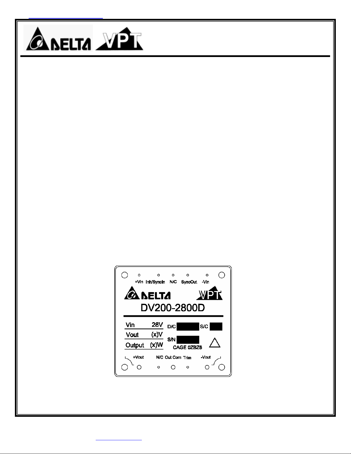
Figure 1 – DV200-2800D DC-DC Converter
(Not To Scale)
Sales Information:
Phone: (425) 353-3010
Fax: (425) 353-4030
E-mail: sales@vpt-inc.com
1
Page 2
DV200-2800D Series
SPECIFICATIONS (T
= -55°C to +100°C, VIN = +28V ± 5%, Full Load, Unless Otherwise Specified)
CASE
ABSOLUTE MAXIMUM RATINGS
Input Voltage (Continuous) 50 VDC Junction Temperature Rise to Case +25°C
Input Voltage (Transient, 1 second) 55 Volts Storage Temperature -65°C to +135°C
Output Power
Power Dissipation (Full Load, T
1,3
200 Watts Lead Solder Temperature (10 seconds) 270°C
= +100°C) 44 Watts Weight (Maximum) 115 grams
CASE
Parameter Conditions
STATIC
INPUT
Voltage
Current
7
Ripple Current Full Load5, 20Hz to 10MHz - - 100 - - 100 mA
Inhibit Pin Input
4
Inhibit Pin Open Circuit Voltage
UVLO Turn On 13.5 14 15.8 13.5 14 15.8 V
UVLO Turn Off
4
+V
OUTPUT
Voltage
+V
Total
3,6,7
Power
±V
3,6,7
Current
±V
Ripple Voltage ±V
Line Regulation
Load Regulation
Cross Regulation
+V
+V
Voltage Trim Full Load
EFFICIENCY Full Load
LOAD FAULT POWER DISSIPATION
CAPACITIVE LOAD
4
SWITCHING FREQUENCY 450 500 550 450 500 550 kHz
SYNC FREQUENCY RANGE
ISOLATION 500 VDC, T
MTBF (MIL-HDBK-217F) GB @ TC = 55°C - 955 - - 955 - kHrs
Continuous 16 28 50 16 28 50 V
Transient, 1 sec - - 55 - - 55 V
Inhibited - 6 10 - 6 10 mA
No Load - 20 80 - 20 80 mA
0 - 1.5 0 - 1.5 V
4
8 9.5 11 8 9.5 11 V
10 12 14 10 12 14 V
OUT TCASE
OUT TCASE
-V
OUT TCASE
-V
OUT TCASE
= 25°C 4.95 5.00 5.05 11.88 12.00 12.12 V
= -55°C to +100°C 4.925 5.00 5.075 11.82 12.00 12.18 V
= 25°C 4.80 5.00 5.20 11.76 12.00 12.24 V
= -55°C to +100°C 4.85 5.00 5.25 11.52 12.00 12.48 V
VIN = 18V to 50V - - 150 - - 175 W
= 16V to 18V - - 90 - - 105 W
V
IN
VIN = 18V to 50V
Either Output
OUT
= 16V to 18V
V
IN
Either Output
VIN = 18V to 50V
Either Output
OUT
VIN = 16V to 18V
Either Output
Full Load5, 20Hz to 10MHz - 50 150 - 50 200 mV
OUT
OUT VIN
-V
OUT VIN
OUT
-V
OUT
-V
OUT
= 18V to 40V - 10 80 - 10 80 mV
= 18V to 40V - 10 200 - 10 200 mV
No Load to Full Load
No Load to Full Load
5
5
V1+ Load 30% - Load 70%
V2+ Load 70% - Load 30%
5
Overload
4
Short Circuit - - 80 - - 80 W
Either Output - - 1000 - - 1000
– VL = 5V
V
H
Duty Cycle = 20% - 80%
= 25°C 100 - - 100 - - MΩ
CASE
DV200-2805D DV200-2812D
Units
Min Typ Max Min Typ Max
p-p
- - 105 - - 122.5 W
- - 63 - - 73.5 W
- - 21 - - 10.2 A
- - 12.6 - - 6.1 A
p-p
- 10 80 - 10 80 mV
- 10 200 - 10 200 mV
- - 550 - - 550 mV
-20 - 10 -20 - 10 %
79 82 - 80 84 - %
- - 80 - - 80 W
µF
450 - 550 450 - 550 kHz
15002DSB
2
Page 3
DV200-2800D Series
SPECIFICATIONS (T
= -55°C to +100°C, V
CASE
= +28V ± 5%, Full Load, Unless Otherwise Specified)
IN
ABSOLUTE MAXIMUM RATINGS
Input Voltage (Continuous) 50 VDC Junction Temperature Rise to Case +25°C
Input Voltage (Transient, 1 second) 55 Volts Storage Temperature -65°C to +135°C
Output Power
Power Dissipation (Full Load, T
1,3
200 Watts Lead Solder Temperature (10 seconds) 270°C
= +100°C) 44 Watts Weight (Maximum) 115 grams
CASE
Parameter Conditions
DYNAMIC
Load Step Output Transient ±V
Load Step Recovery2
Line Step Output Transient
Line Step Recovery
Turn On Delay ±V
Turn On Overshoot
2, 4
4
±V
OUT
Half Load to Full Load
OUT
V
= 18V to 40V
IN
OUT
V
= 0V to 28V
IN
DV200-2805D DV200-2812D
Min Typ Max Min Typ Max
- - 500 - - 600 mV
- - 500 - - 500
- 300 600 - 600 1200 mV
- 300 500 - 300 500
- 20 30 - 20 30 mSec
- - 50 - - 50 mV
Units
µSec
µSec
Notes: 1. Dependant on output voltage.
2. Time for output voltage to settle within 1% of its nominal value.
3. Derate linearly to 0 at 110°C.
4. Verified by qualification testing.
5. Half load at +V
6. Up to 70% of the total power or current can be drawn from any one of the two outputs.
7. 100% output power available for VIN = 18V to 50V and only 60% output power available for VIN = 16V to 18V.
and half load at –V
OUT
OUT
.
PK
PK
PK
15002DSB
3
Page 4
DV200-2800D Series
SPECIFICATIONS (T
= -55°C to +100°C, VIN = +28V ± 5%, Full Load, Unless Otherwise Specified)
CASE
ABSOLUTE MAXIMUM RATINGS
Input Voltage (Continuous) 50 VDC Junction Temperature Rise to Case +25°C
Input Voltage (Transient, 1 second) 55 Volts Storage Temperature -65°C to +135°C
Output Power
Power Dissipation (Full Load, T
1,3
200 Watts Lead Solder Temperature (10 seconds) 270°C
= +100°C) 44 Watts Weight (Maximum) 115 grams
CASE
Parameter Conditions
STATIC
INPUT
Voltage
Current
7
Ripple Current Full Load5, 20Hz to 10MHz - - 100 mA
Inhibit Pin Input
4
Inhibit Pin Open Circuit Voltage
UVLO Turn On 13.5 14 15.8 V
UVLO Turn Off
4
+V
OUTPUT
Voltage
+V
Total
3,6,7
Power
±V
3,6,7
Current
±V
Ripple Voltage ±V
Line Regulation
Load Regulation
Cross Regulation
+V
+V
Voltage Trim Full Load
EFFICIENCY Full Load
LOAD FAULT POWER DISSIPATION
CAPACITIVE LOAD
4
SWITCHING FREQUENCY 450 500 550 kHz
SYNC FREQUENCY RANGE
ISOLATION 500 VDC, T
MTBF (MIL-HDBK-217F) GB @ TC = 55°C - 955 - kHrs
Continuous 16 28 50 V
Transient, 1 sec - - 55 V
Inhibited - 6 10 mA
No Load - 20 80 mA
0 - 1.5 V
4
8 9.5 11 V
10 12 14 V
OUT TCASE
OUT TCASE
-V
OUT TCASE
-V
OUT TCASE
= 25°C 14.85 15.00 15.15 V
= -55°C to +100°C 14.775 15.00 15.225 V
= 25°C 14.70 15.00 15.30 V
= -55°C to +100°C 14.40 15.00 15.60 V
VIN = 18V to 50V - - 200 W
= 16V to 18V - - 120 W
V
IN
VIN = 18V to 50V
Either Output
OUT
= 16V to 18V
V
IN
Either Output
VIN = 18V to 50V
Either Output
OUT
VIN = 16V to 18V
Either Output
Full Load5, 20Hz to 10MHz - 50 200 mV
OUT
OUT VIN
-V
OUT VIN
OUT
-V
OUT
-V
OUT
= 18V to 40V - 10 80 mV
= 18V to 40V - 10 200 mV
No Load to Full Load
No Load to Full Load
5
5
V1+ Load 30% - Load 70%
V2+ Load 70% - Load 30%
5
Overload
4
Short Circuit - - 80 W
Either Output - - 1000
– VL = 5V
V
H
Duty Cycle = 20% - 80%
= 25°C 100 - - MΩ
CASE
DV200-2815D
Units
Min Typ Max
p-p
- - 140 W
- - 84 W
- - 9.3 A
- - 5.6 A
p-p
- 10 80 mV
- 10 200 mV
- - 550 mV
-20 - 10 %
81 85 - %
- - 80 W
µF
450 - 550 kHz
15002DSB
4
Page 5

DV200-2800D Series
SPECIFICATIONS (T
= -55°C to +100°C, VIN = +28V ± 5%, Full Load
CASE
5
, Unless Otherwise Specified)
ABSOLUTE MAXIMUM RATINGS
Input Voltage (Continuous) 50 VDC Junction Temperature Rise to Case +25°C
Input Voltage (Transient, 1 second) 55 Volts Storage Temperature -65°C to +135°C
Output Power
Power Dissipation (Full Load, T
1,3
200 Watts Lead Solder Temperature (10 seconds) 270°C
= +100°C) 44 Watts Weight (Maximum) 115 grams
CASE
Parameter Conditions
DYNAMIC
Load Step Output Transient ±V
Load Step Recovery2
Line Step Output Transient
Line Step Recovery
Turn On Delay ±V
Turn On Overshoot
2, 4
4
±V
OUT
Half Load to Full Load
OUT
V
= 18V to 40V
IN
OUT
V
= 0V to 28V
IN
DV200-2815D
Min Typ Max
- - 600 mV
- - 500
- 600 1200 mV
- 300 500
- 20 30 mSec
- - 50 mV
Units
PK
µSec
PK
µSec
PK
Notes: 1. Dependant on output voltage.
2. Time for output voltage to settle within 1% of its nominal value.
3. Derate linearly to 0 at 110°C.
4. Verified by qualification testing.
5. Half load at +V
6. Up to 70% of the total power or current can be drawn from any one of the two outputs.
7. 100% output power available for VIN = 18V to 50V and only 60% output power available for VIN = 16V to 18V.
and half load at –V
OUT
OUT
.
15002DSB
5
Page 6

SHUTDO
SU
Y
SU
Y
BLOCK DIAGRAM
DV200-2800D Series
PIN 6
+V OUT
PIN 5
28V IN
IN COM
PIN 1
UNDER
VOLTAGE
WN
PRIMARY
HOUSEKEEPING
PPL
INH / SYNC IN
PIN 4
SYNC OUT
PIN 2
CONNECTION DIAGRAM
PWM
CONTROL
Q1
Figure 2
MAGNETIC
FEEDBACK
VOLTAGE AND
CURRENT
AMPLIFIERS
SECONDARY
HOUSEKEEPING
PPL
PIN 8
OUT COM
PIN 10
-V OUT
PIN 9
TRIM
5
28V IN
+V OUT
2200PF
4
INH/SYNC IN
28 Vdc OUT COM
+
-
1
IN COM
Figure 3
15002DSB
-V OUT
6
LOAD
8
LOAD
10
6
Page 7

INHIBIT DRIVE CONNECTION DIAGRAMS
DV200-2800D Series
OPTOISOLATOR
INH/SYNCIN
4
25K
+
10V
-
1IN COM
Figure 4 – Isolated Inhibit Drive and Internal Equivalent Circuit
15002DSB
7
Page 8

OUTPUT VOLTAGE TRIM
10K
-
+
+
-
2.5V
15K
Ri
DV200-2805D DV200-2812D DV200-2815D
+V OUT
PIN 6
TRIM
PIN 9
OUT COM
PIN 8
-V OUT
PIN 10
The output voltage can be trimmed down by
connecting a resistor between the TRIM pin
R-TRIM
(TRIM DOWN)
(PIN 9) and the +V OUT pin (PIN 6), or can
be trimmed up by connecting a resistor
between the TRIM pin (PIN 9) and the OUT
COM pin (PIN 8). The maximum trim range
is +10% up and –20% down. The
R-TRIM
(TRIM UP)
appropriate resistor values versus the
output voltage are given in the trim table
below.
Figure 5 – Output Voltage Trim
DV200-2800D Series
±V
(V) R
OUT
5.5 35k 13.2 5.8k 16.50 1.7k
5.4 47.5k 13.0 10k 16.25 5k
5.3 68.3k 12.8 16.2k 16.00 10k
5.2 110k 12.6 26.6k 15.75 18.3k
5.1 235k 12.4 47.3k 15.50 35k
5.0 - 12.2 109k 15.25 85k
4.9 225k 12.0 - 15.00 -
4.8 100k 11.8 454k 14.75 475k
4.7 58.3k 11.6 213k 14.50 225k
4.6 37.5k 11.4 134k 14.25 142k
4.5 25k 11.2 94k 14.00 100k
4.4 16.7k 11.0 70.1k 13.75 75k
4.3 10.7k 10.8 54.3k 13.50 58.3k
4.2 6.3k 10.6 42.9k 13.25 46.4k
4.1 2.8k 10.4 34.4k 13.00 37.5k
4.0 0 10.2 27.8k 12.75 30.6k
10.0 22.5k 12.50 25k
9.8 18.2k 12.25 20.5k
9.6 14.6k 12.00 16.7k
(Ω) ±V
TRIM
(V) R
OUT
(Ω) ±V
TRIM
(V) R
OUT
TRIM
(Ω)
15002DSB
8
Page 9

PACKAGE SPECIFICATIONS
DV200-2800D Series
TOP VIEW
SIDE VIEW
Figure 6 – Package and Pinout
(Dimensional Limits are ±0.005” Unless Otherwise Stated)
PIN FUNCTION
1 IN COM
2 SYNC OUT
3 N/C
4 INH / SYNC IN
5 28V IN
6 +V OUT
7 N/C
8 OUT COM
9 TRIM
10 -V OUT
15002DSB
9
Page 10

PACKAGE PIN DESCRIPTION
Pin Function Description
1 IN COM Input Common Connection
2 SYNC OUT Output Synchronization Signal
3 N/C No Connection
DV200-2800D Series
4
5 28V IN Positive Input Voltage Connection
6 +V OUT Positive Output Voltage Connection
7 N/C No Connection
8 OUT COM Output Common Connection
9 TRIM Trim Output Voltage to +10%, -20% of Nominal Value
10 -V OUT Negative Output Voltage Connection
INH /
SYNC IN
Logic Low = Disabled Output. Unconnected or open collector TTL or Square-wave
Synchronization Signal = Enabled Output.
ENVIRONMENTAL SCREENING
Screening MIL-STD-883
Pre-Cap Inspection IPC-A-610 Class II
Temperature Cycling -55°C, 100°C, 10 cycles
Burn-In
Final Electrical
96 hours at +100°C
12 hours at +100°C
100% at -55°C, 25°C, 100°C
100% at 25°C
1
Standard
(No Suffix)
• •
•
•
Military
/ML
•
•
•
Final Inspection Method 2009
• •
Note: 1. 100% R&R testing at –55°C, +25°C, and +100°C with all test data included in product
shipment.
15002DSB
10
Page 11

ORDERING INFORMATION
DV200- 28 05 D /ML - XXX
1 2 3 4 5 6
(1) (2) (3)
DV200-2800D Series
Product Series
DV200-
Nominal Input
Voltage
28
28 Volts
Output Voltage
05
12
15
±5 Volts
±12 Volts
±15 Volts
(4) (5) (6)
Number of Outputs Screening Code
D
Dual
None
/ML
Standard
Military
Additional Screening
Code
Contact Sales
Please contact your sales representative or the VPT Inc. Sales Department for more information
concerning additional environmental screening and testing, different input voltage, output voltage,
power requirement, source inspection, and/or special element evaluation for space or other higher
quality applications.
CONTACT INFORMATION
To request a quotation or place orders please contact your sales representative or the VPT Inc. Sales
Department at:
Phone: (425) 353-3010
Fax: (425) 353-4030
E-mail: sales@vpt-inc.com
All information contained in this datasheet is believed to be accurate, however, no responsibility is assumed for possible errors
or omissions. The products or specifications contained herein are subject to change without notice.
15002DSB
11
 Loading...