

Page 1
PROGRAMMABLE
DELAY CHIP
ClockWorks™
SY10E195
SY100E195
FEATURES
■ Up to 2ns delay range
■ Extended 100E V
EE range of –4.2V to –5.5V
■ ≈20ps/digital step resolution
■ >1GHz bandwidth
■ On-chip cascade circuitry
■ 75KkΩ input pulldown resistor
■ Fully compatible with Motorola MC10E/100E195
■ Available in 28-pin PLCC package
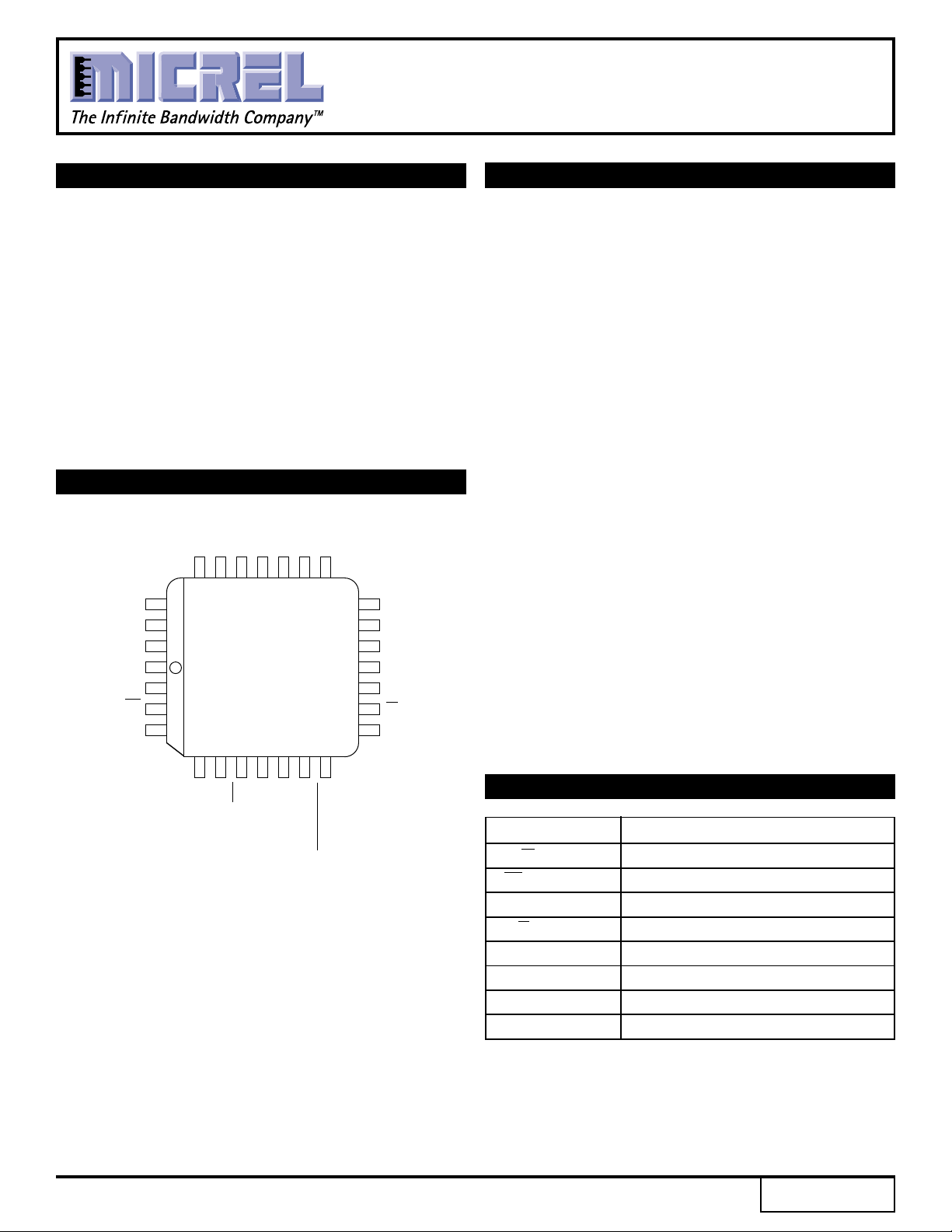
PIN CONFIGURATION
D4
D5
PLCC
J28-1
D6
D7
NC
18
NC
17
NC
16
VCC
15
VCCO
14
Q
13
Q
12
VCCO
D1
D0
LEN
VEE
IN
IN
VBB
D2
D3
25
24 23 22 21 20 19
26
27
28
1
2
3
4
TOP VIEW
567891011
DESCRIPTION
The SY10/100E195 are programmable delay chips
(PDCs) designed primarily for clock de-skewing and timing
adjustment. They provide variable delay of a differential
ECL input transition.
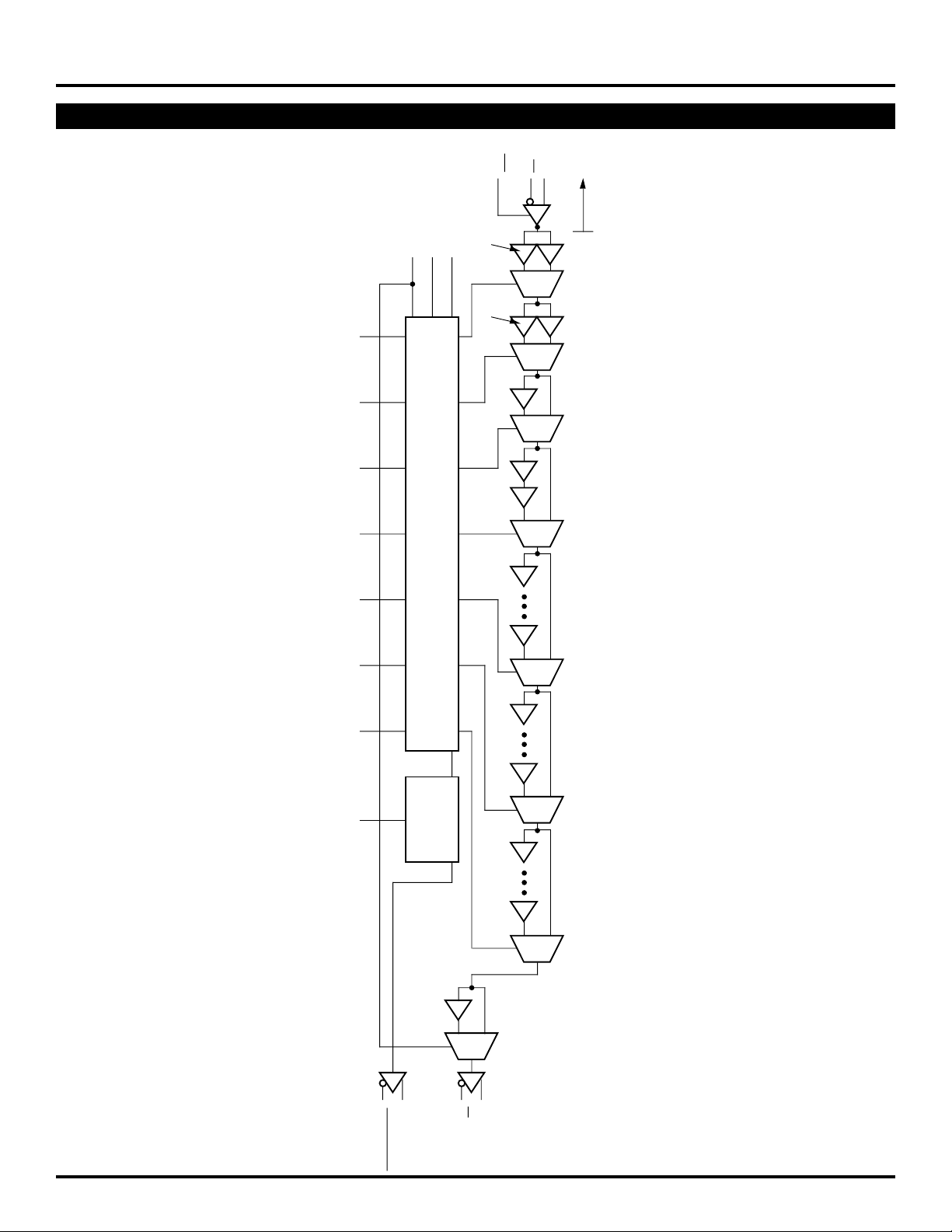
The delay section consists of a chain of gates
organized as shown in the logic diagram. The first two
delay elements feature gates that have been modified to
have delays 1.25 and 1.5 times the basic gate delay of
approximately 80ps. These two elements provide the
E195 with a digitally-selectable resolution of
approximately 20ps. The required device delay is selected
by the seven address inputs D[0:6], which are latched
on-chip by a high signal on the latch enable (LEN) control.
If the LEN signal is either LOW or left floating, then the
latch is transparent.
Because the delay programmability of the E195 is
achieved by purely differential ECL gate delays, the
device will operate at frequencies of >1GHz, while
maintaining over 600mV of output swing.
The E195 thus offers very fine resolution, at very high
frequencies, selectable entirely from a digital input,
allowing for very accurate system clock timing.
An eighth latched input, D7, is provided for cascading
multiple PDCs for increased programmable range. The
cascade logic allows full control of multiple PDCs, at the
expense of only a single added line to the data bus for
each additional PDC, without the need for any external
gating.
NC
NC
EN
SET MIN
SET MAX
CASCADE
CASCADE
PIN NAMES
Pin Function
IN/IN Signal Input
EN Input Enable
D[0:7] Mux Select Inputs
Q/Q Signal Output
LEN Latch Enable
SET MIN Minimum Delay Set
SET MAX Maximum Delay Set
CASCADE Cascade Signal
1
Rev.: E Amendment: /0
Issue Date: October, 1998
Page 2
Micrel
BLOCK DIAGRAM
ClockWorks™
SY10E195
SY100E195
IN
V
BB
SET MAX
SET MIN
EN
IN
LEN
*1.25
*1.5
D
0
D
1
D
2
1
1
0
1
1
0
1
1
0
1
1
7-Bit Latch
1
D
3
0
4 gates
D
4
*Delays are 25% or 50% longer than
standard (standard = 80ps).
D
5
D
6
D
7
D
CASCADE
CASCADE
LEN
Latch
Q
Cascade
1
1
Q
1
0
8 gates
1
0
16 gates
1
0
0
Q
2
Page 3

ClockWorks™
SY10E195
Micrel
SY100E195
DC ELECTRICAL CHARACTERISTICS
VEE = VEE (Min.) to VEE (Max.); VCC = GND
T
A = 0°CTA = +25°CTA = +85°C
Symbol Parameter Min. Typ. Max. Min. Typ. Max. Min. Typ. Max. Unit Condition
IIH Input HIGH Current — — 150 — — 150 — — 150 µA—
EE Power Supply Current mA —
I
10E — 130 156 — 130 156 — 130 156
100E — 130 156 — 130 156 — 150 179
3
Page 4

ClockWorks™
SY10E195
Micrel
SY100E195
AC ELECTRICAL CHARACTERISTICS
VEE = VEE (Min.) to VEE (Max.); VCC = GND
TA = 0°CTA = +25°CTA = +85°C
Symbol Parameter Min. Typ. Max. Min. Typ. Max. Min. Typ. Max. Unit Condition
PLH Propagation Delay to Output ps —
t
tPHL IN to Q; Tap = 0 1210 1360 1510 1240 1390 1540 1440 1590 1765
IN to Q; Tap = 127 3320 3570 3820 3380 3630 3880 3920 4270 4720
EN to Q; Tap = 0 1250 1450 1650 1275 1475 1675 1350 1650 1950
D7 to CASCADE 300 450 700 300 450 700 300 450 700
RANGE Programmable Range 2000 2175 — 2050 2240 — 2375 2580 — ps —
t
tPD (max.) – tPD (min.)
∆t Step Delay ps 6
D
0 High — 17 — — 17.5 — — 21 —
D1 High — 34 — — 35 — — 42 —
D2 High 55 68 105 55 70 105 65 84 120
D3 High 115 136 180 115 140 180 140 168 205
D4 High 250 272 325 250 280 325 305 336 380
D5 High 505 544 620 515 560 620 620 672 740
D6 High 1000 1088 1190 1030 1120 1220 1240 1344 1450
Lin Linearity D1 D0 —D1 D0 —D1 D0 —— 7
tskew Duty Cycle Skew, tPHL–tPLH — ±30 — — ±30 — — ±30 — ps 1
S Set-up Time ps
t
D to LEN 200 0 — 200 0 — 200 0 —
D to IN 800 — — 800 — — 800 — — 2
EN to IN 200 — — 200 — — 200 — — 3
H Hold Time ps
t
LEN to D 500 250 — 500 250 — 500 250 —
IN to EN 0 — — 0 — — 0 — — 4
R Release Time ps
t
EN to IN 300 — — 300 — — 300 — — 5
SET MAX to LEN 800 — — 800 — — 800 — —
SET MIN to LEN 800 — — 800 — — 800 — —
tjit Jitter — <5 — — <5 — — <5 — ps 8
r Rise/Fall Times ps —
t
tf 20–80% (Q) 125 225 325 125 225 325 125 225 325
20–80% (CASCADE) 300 450 650 300 450 650 300 450 650
NOTES:
2. Duty cycle skew guaranteed only for differential operation measured from the cross point of the input to the cross point of the output.
3. This set-up time defines the amount of time prior to the input signal the delay tap of the device must be set.
4. This set-up time is the minimum time that EN must be asserted prior to the next transition of IN/IN to prevent an output response greater than ±75mV to
that IN/IN transition.
5. This hold time is the minimum time that EN must remain asserted after a negative going IN or positive going IN to prevent an output response greater than
±75mV to that IN/IN transition.
6. This release time is the minimum time that EN must be deasserted prior to the next IN/IN transition to ensure an output response that meets the specified
IN to Q propagation delay and transition times.
7. Specification limits represent the amount of delay added with the assertion of each individual delay control pin. The various combinations of asserted delay
control inputs will typically realize D0 resolution steps across the specified programmable range.
8. The linearity specification guarantees to which delay control input the programmable steps will be monotonic (i.e. increasing delay steps for increasing
binary counts on the control inputs Dn). Typically, the device will be monotonic to the D0 input, however, under worst case conditions and process variation,
delays could decrease slightly with increasing binary counts when the D0 input is the LSB. With the D1 input as the LSB, the device is guaranteed to be
monotonic over all specified environmental conditions and process variation.
9. The jitter of the device is less than what can be measured without resorting to very tedious and specialized measurement techniques.
4
Page 5

Micrel
APPLICATIONS INFORMATION
7
A
ClockWorks™
SY10E195
SY100E195
ADDRESS BUS (A0 – A6)
6
5
4
D
E196
Chip #1
EN
7
D
D
D
VCC
VCCO
Q
Q
VCCO
SET MAX
CASCADE
SET MIN
Figure 1. Cascading Interconnect Architecture
CASCADE
Input
D
1
D
0
LEN
VEE
IN
IN
VBB
2
3
D
D
Cascading Multiple E195s
To increase the programmable range of the E195,
internal cascade circuitry has been included. This circuitry
allows for the cascading of multiple E195s without the
need for any external gating. Furthermore, this capability
requires only one more address line per added E195.
Obviously, cascading multiple PDCs will result in a larger
programmable range; however, this increase is at the
expense of a longer minimum delay.
Figure 1 illustrates the interconnect scheme for
cascading two E195s. As can be seen, this scheme can
easily be expanded for larger E195 chains. The D7 input
of the E195 is the cascade control pin. With the
interconnect scheme of Figure 1, when D7 is asserted, it
signals the need for a larger programmable range than
is achievable with a single device.
An expansion of the latch section of the block diagram
is pictured below. Use of this diagram will simplify the
explanation of how the cascade circuitry works. When
D7 of chip #1 above is low, the cascade output will also
be low, while the cascade bar output will be a logical
high. In this condition, the SET MIN pin of chip #2 will
be asserted and, thus, all of the latches of chip #2 will
be reset and the device will be set at its minimum delay.
Since the RESET and SET inputs of the latches are
overriding, any changes on the A0–A6 address bus will
not affect the operation of chip #2.
D
1
D
0
LEN
VEE
IN
IN
VBB
4
3
2
D
D
D
E196
Chip #2
EN
6
5
D
D
SET MIN
SET MAX
7
D
VCC
VCCO
VCCO
CASCADE
CASCADE
Q
Q
Output
Chip #1, on the other hand, will have both SET MIN
and SET MAX de-asserted so that its delay will be
controlled entirely by the address bus A0–A6. If the delay
needed is greater than can be achieved with 31.75 gate
delays (1111111 on the A0–A6 address bus), D7 will be
asserted to signal the need to cascade the delay to the
next E195 device. When D7 is asserted, the SET MIN
pin of chip #2 will be de-asserted and the delay will be
controlled by the A0–A6 address bus. Chip #1, on the
other hand, will have its SET MAX pin asserted, resulting
in the device delay to be independent of the A0–A6
address bus.
When the SET MAX pin of chip #1 is asserted, the D0
and D1 latches will be reset while the rest of the latches
will be set. In addition, to maintain monotonicity, an
additional gate delay is selected in the cascade circuitry.
As a result, when D7 of chip #1 is asserted, the delay
increases from 31.75 gates to 32 gates. A 32-gate delay
is the maximum delay setting for the E195.
To expand this cascading scheme to more devices,
one simply needs to connect the D7 input and CASCADE
outputs of the current most significant E195 to the new
most significant E195 in the same manner as pictured in
Figure 1. The only addition to the logic is the increase
of one line to the address bus for cascade control of the
second PDC.
5
Page 6

Micrel
SET MAX
SET MIN
Reset
Reset
Reset
Set
Reset
Reset
LEN
LEN
LEN
ClockWorks™
SY10E195
SY100E195
D
0
Bit 0
Q
0
D
1
Bit 1
Q
1
D
2
Bit 2
Q
2
Set
Reset
Set
Reset
Set
Reset
Set
Reset
LEN
LEN
LEN
LEN
D
3
Bit 3
Q
3
D
4
Bit 4
Q
4
D
5
Bit 5
Q
5
D
6
Bit 6
Q
6
To Select Multiplexers
Figure 2. Expansion of the
Latch Section of the E195
Block Diagram
LEN
CASCADE
D
7
Bit 7
Q
7
CASCADE
PRODUCT ORDERING CODE
Ordering Package Operating
Code Type Range
SY10E195JC J28-1 Commercial
SY10E195JCTR J28-1 Commercial
SY100E195JC J28-1 Commercial
SY100E195JCTR J28-1 Commercial
6
Page 7

Micrel
28 LEAD PLCC (J28-1)
ClockWorks™
SY10E195
SY100E195
Rev. 03
7
Page 8

Micrel
ClockWorks™
SY10E195
SY100E195
MICREL-SYNERGY 3250 SCOTT BOULEVARD SANTA CLARA CA 95054 USA
TEL + 1 (408) 980-9191 FAX + 1 (408) 914-7878 WEB http://www.micrel.com
This information is believed to be accurate and reliable, however no responsibility is assumed by Micrel for its use nor for any infringement of patents or
other rights of third parties resulting from its use. No license is granted by implication or otherwise under any patent or patent right of Micrel Inc.
© 2000 Micrel Incorporated
8
 Loading...