

Page 1
ENHANCED
DIFFERENTIAL
RECEIVER
SY10EL16VA-VF
SY100EL16VA-VF
FEATURES
■ 3.3V and 5V power supply options
■ 250ps propagation delay
■ Very high voltage gain vs. standard EL16 or EL16V
■ Ideal for Pulse Amplifier and Limiting Amplifier
applications
■ Data synchronous Enable/Disable (/EN) on QHG
HG provides for complete glitchless gating of the
/Q
outputs
■ Ideal for gating timing signals
■ Complete solution for high quality, high frequency
crystal oscillator applications
■ Internal 75K Ohm input pull-down resistors
■ Available in both 8 and 16-pin SOIC package; 8 and
10-pin (3mm) MSOP and in DIE form
and
PIN NAMES
Pin Function
D Data Inputs
Q Data Outputs
QHG Data Outputs w/High Gain
VBB Reference Voltage Output
/EN Enable Input
TRUTH TABLE
/EN QHG Output
0 Data
1 Logic Low
DESCRIPTION
The SY10/100EL16VA-VF are differential receivers.
The devices are equivalent to SY10/100EL16 or SY10/
100EL16V with enhanced capabilities. The QHG, /QHG
outputs have a DC gain several times larger than the DC
gain of the Q output.
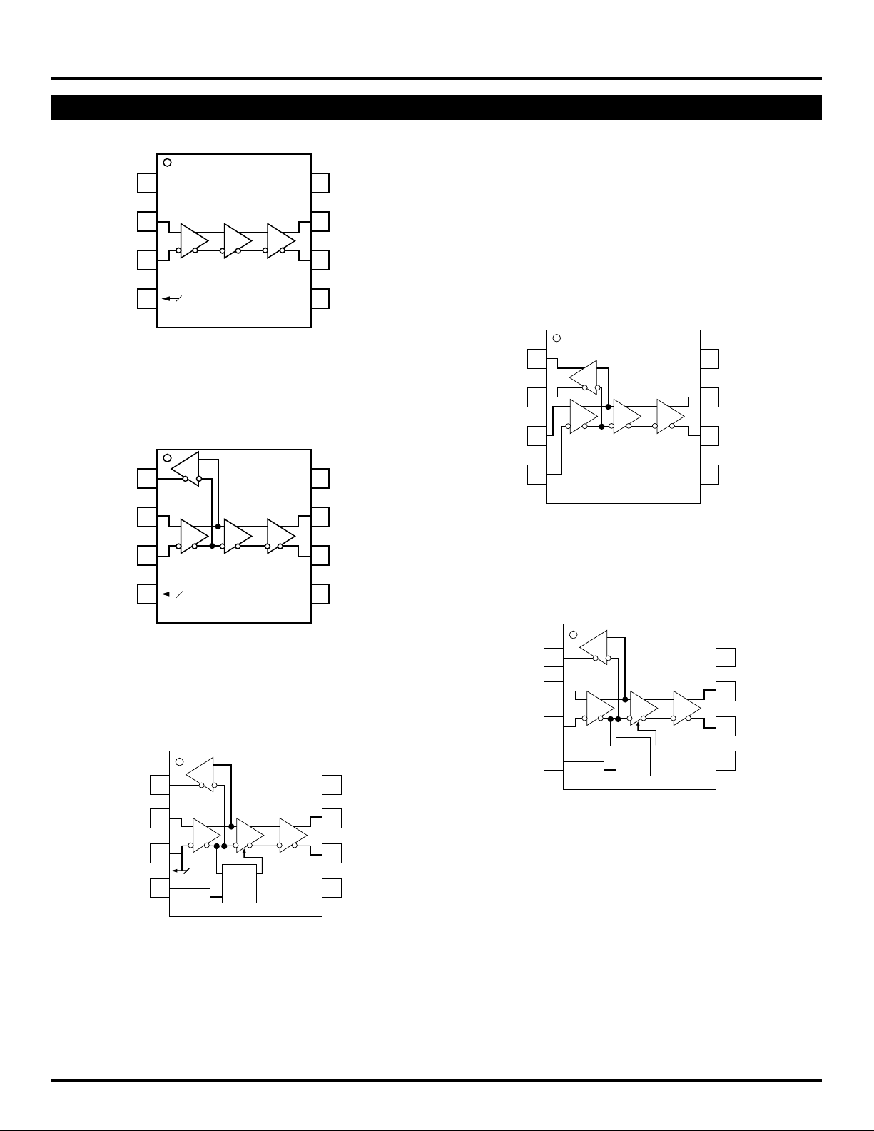
The SY10/100EL16VA have an identical pinout to the
SY10/100EL16 or SY10/100EL16V. It provides a VBB
output for either single-ended application or as a DC
bias for AC coupling to the device.
The SY10/100EL16VB are very similar to the SY10/
100EL16VA. The /Q output is provided for feedback
purposes.
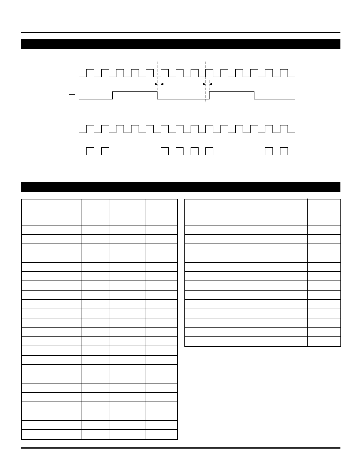
The SY10/100EL16VC provides an /EN input which is
synchronized with the data input (D) signal in a way that
provides glitchless gating of the QHG and /QHG outputs. When
the /EN signal is LOW, the input is passed to the outputs and
the data output equals the data input. When the data input is
HIGH and the /EN goes HIGH, it will force the QHG
the /QHG HIGH on the next negative transition of the data
input. If the data input is LOW when the /EN goes HIGH, the
next data transition to a HIGH is ignored and QHG remains
LOW and /QHG remains HIGH. The next positive transition of
the data input is not passed on to the data outputs under these
conditions. The QHG and /QHG outputs remain in their disabled state as long as the /EN input is held HIGH. The /EN
input has no influence on the /Q output and the data input is
passed on (inverted) to this output whether /EN is HIGH or
LOW. This configuration is ideal for crystal oscillator applications, where the oscillator can be free running and gated on
and off synchronously without adding extra counts to the
output.
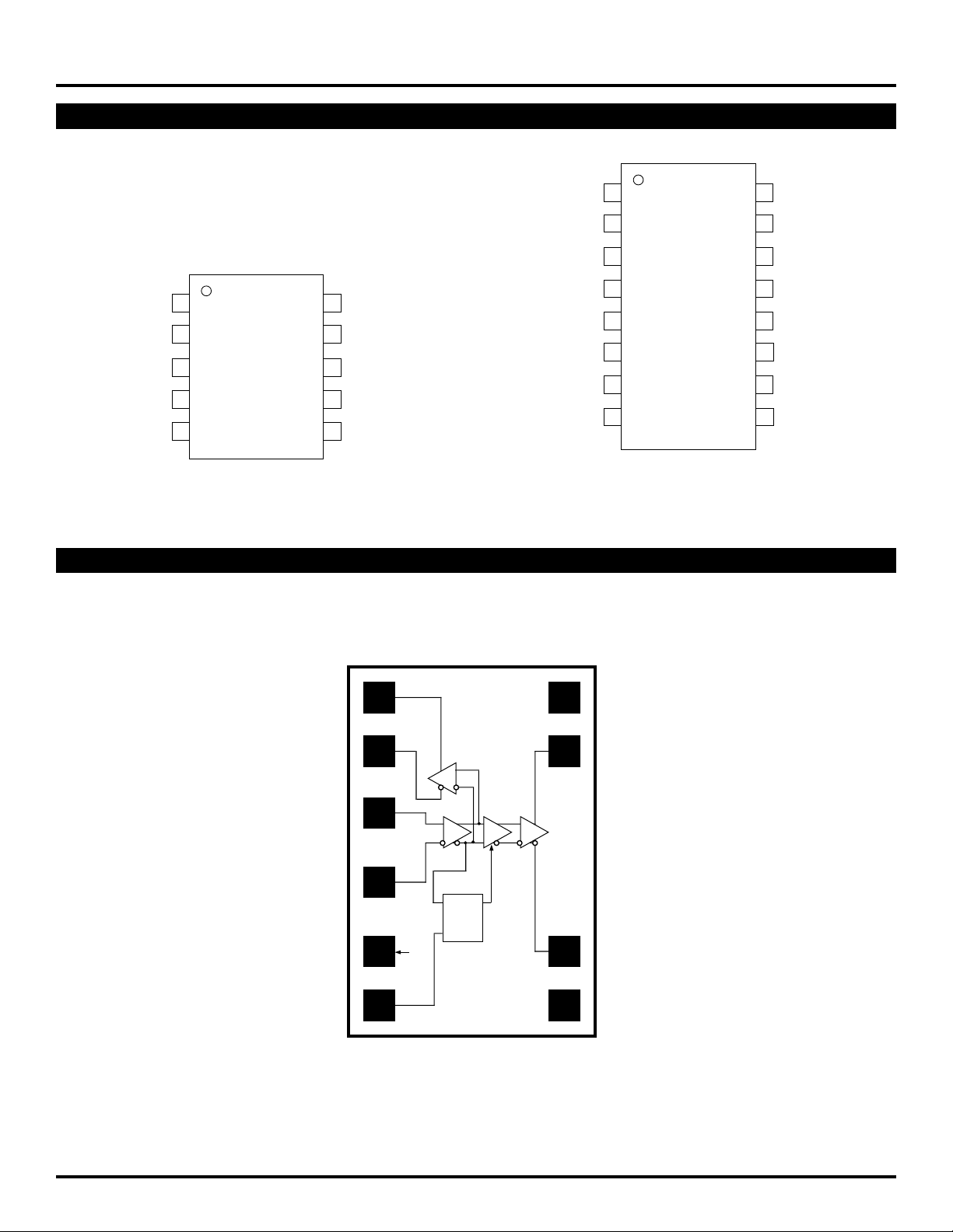
The SY10/100EL16VD provides the flexibility of all the
combinations in DIE form, in 16-pin 150mil SOIC package or
in 10-pin MSOP package. The 16-pin SOIC and 10-pin MSOP
packages are ideal for prototyping DIE applications.
The SY10/100EL16VE are similar to the SY10/100EL16VB
where the Q, /Q output is made available differently. In this
package option, VBB is no longer provided.
The SY10/100EL16VF are similar to the SY10/100EL16VC,
offering the D, /D inputs rather than the VBB output.
LOW and
Rev.: L Amendment: /1
1
Issue Date: July 2000
Page 2
Micrel
PIN CONFIGURATION/BLOCK DIAGRAM
SY10EL16VA-VF
SY100EL16VA-VF
NC
/D
VBB
1
2
D
3
4
8
VCC
7
QHG
6
/QHG
5
VEE
SY10/100EL16VA
5V/3.3V Differential Receiver w/High Gain
(Available in 8-pin SOIC or 8-pin MSOP)
8
1
1
Q
/Q
2
2
D
D
/D
3
3
D
V
BB
BB
V
4
4
8
VCC
VCC
7
7
QHG
QHG
6
6
/QHG
5
5
VEE
VEE
8
V
CC
7
QHG
6
/QHG
5
VEE
/Q
/D
1
Q
2
3
D
4
SY10/100EL16VE
EL16VB w/Differential Q, QB output (no VBB)
(Available in 8-pin SOIC or 8-pin MSOP)
SY10/100EL16VB
EL16VA w/Extra QB output
(Available in 8-pin SOIC or 8-pin MSOP)
/Q
V
BB
/EN
1
2
D
3
V
BB
4
LEN Q
LATCH
D
OE
8
7
6
5
SY10/100EL16VC
EL16VB w/Enable Input
(Available in 8-pin SOIC or 8-pin MSOP)
V
Q
/Q
V
CC
HG
EE
HG
/Q
/D
/EN
1
2
D
3
BB
4
LEN Q
LATCH
D
OE
8
7
6
5
SY10/100EL16VF
EL16VC w/Differential Data Input
(Available in 8-pin SOIC or 8-pin MSOP)
V
Q
/Q
V
CC
HG
HG
EE
2
Page 3
Micrel
PIN CONFIGURATION/BLOCK DIAGRAM
SY10EL16VA-VF
SY100EL16VA-VF
Q
/Q
D
/D
VBB
EL16VDXC packaged in 10-pin MSOP
DIE LAYOUT
1
2
3
4
5
MSOP
K10-1
SY10/100EL16VDKC
All options in DIE form w/Extra Q output and VBB output
VCC
10
QHG
9
/QHG
8
VEE
7
/EN
6
Die Size (mils) 39. X 52. X 14.5
V
NC
/Q
/D
BB
NC
NC
1
2
Q
3
4
D
5
6
7
8
SOIC
Z16-2
NC
16
V
CC
15
Q
HG
14
13
/Q
HG
V
EE
12
11
/EN
NC
10
NC
9
SY10/100EL16VDZC
EL16VDXC packaged in 16-pin SOIC
V
/EN
/Q
/D
BB
Q
V
CC
Q
HG
D
OE
LENDQ
LATCH
V
BB
/Q
HG
EE
V
SY10/100EL16VDXC
DIE
TOP VIEW
3
Page 4
Micrel
SY10EL16VA-VF
SY100EL16VA-VF
DC ELECTRICAL CHARACTERISTICS
(1)
VEE = VEE (Min) to VEE (Max), VCC = GND
TA = –40°CTA = 0°CTA = +25°CTA = +85°C
Symbol Parameter Min. Typ. Max. Min. Typ. Max. Min. Typ. Max. Min. Typ. Max. Unit
EE Power Supply mA
I
Current 10EL — — 40 — — 40 — — 40 — — 40
100EL — — 40 — — 40 — — 40 — — 46
BB Output Reference V
V
Voltage 10EL –1.43 — –1.30 –1.38 — –1.27 –1.35 — –1.25 –1.31 — –1.19
100EL –1.38 — –1.26 –1.38 — –1.26 –1.38 — –1.26 –1.38 — –1.26
I
IH Input HIGH Current — — 150 — — 150 — — 150 — — 150 µA
NOTE:
1. Parametric values specified at: 10/100EL16VA-VF Series: -3.0V to -5.5V.
AC ELECTRICAL CHARACTERISTICS
(4)
VEE = VEE (Min) to VEE (Max), VCC = GND
TA = –40°CTA = 0°CTA = +25°CTA = +85°C
Symbol Parameter Min. Typ. Max. Min. Typ. Max. Min. Typ. Max. Min. Typ. Max. Unit
PLH Propagation Delay to ps
t
tPHL Q, /Q Output D (Diff) — — 350 — — 350 — — 350 — — 380
D (SE) — — 400 — — 400 — — 400 — — 430
QHG, /QHG Output
D (Diff) — — 650 — — 650 — — 650 — — 730
D (SE) — — 700 — — 700 — — 700 — — 780
tS Setup Time /EN — 150 — — 150 — — 150 — — 150 — ps
tH Hold Time /EN — 150 — — 150 — — 150 — — 150 — ps
skew Duty Cycle Skew
t
VPP Minimum Input Swing
VCMR Common Mode Range
tr Output Q 100 225 350 100 225 350 100 225 350 100 225 350 ps
tf Rise/Fall Time
(20% TO 80%)
(1)
(Diff) — 5 — — 5 20 — 5 20 — 5 20 ps
(2)
150 — — 150 — — 150 — — 150 — — mV
(3)
–1.3 — –0.4 –1.4 — –0.4 –1.4 — –0.4 –1.4 — –0.4 V
NOTES:
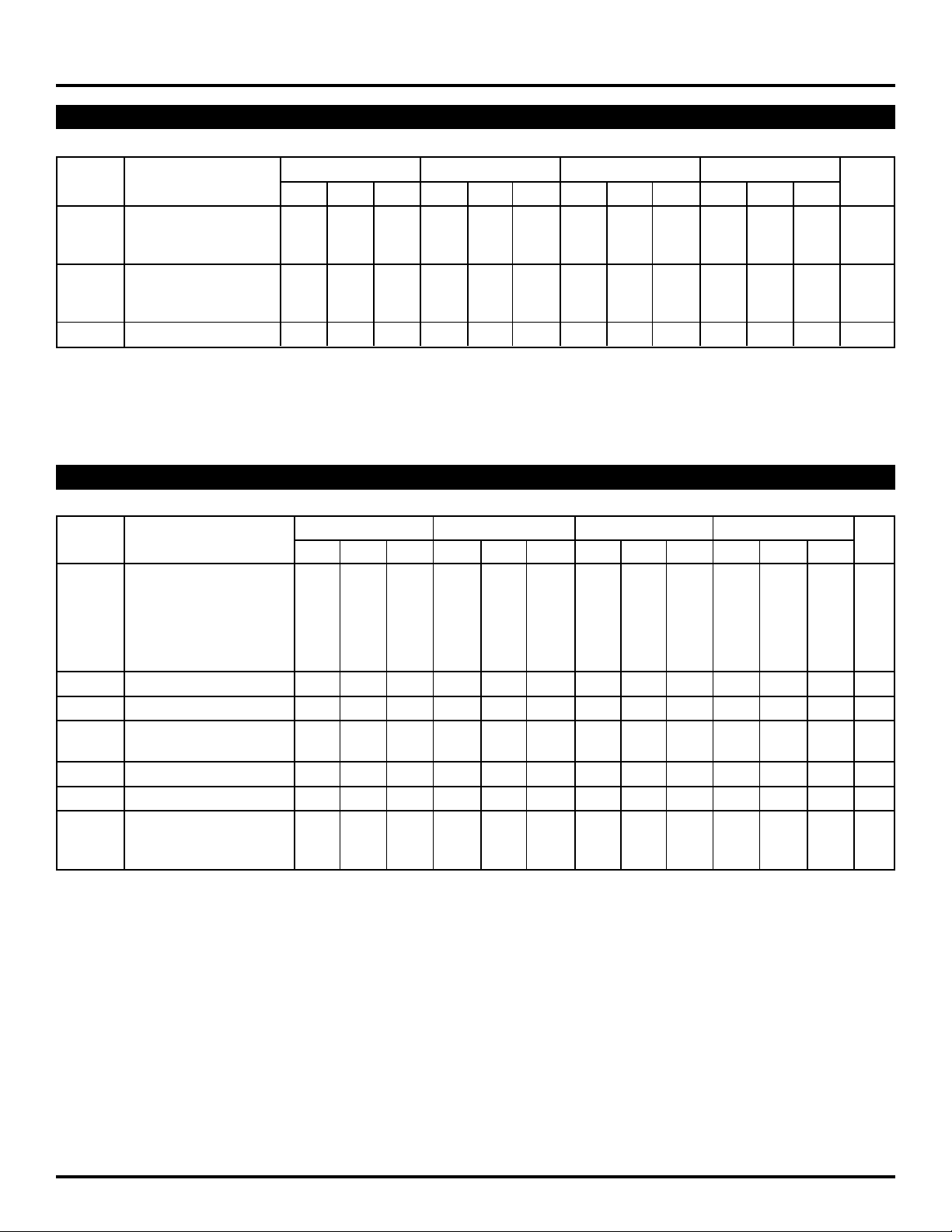
1. Duty cycle skew is the difference between a t
2. Minimum input swing for which AC parameters are guaranteed. The device has a DC gain of ≈ 40 to Q, /Q outputs and a DC gain of ≈ 200 or higher to
/QHG/QHG outputs.
3. The CMR range is referenced to the most positive side of the differential input signal. Normal operation is obtained if the HIGH level falls within the specified
range and the peak-to-peak voltage lies between VPP min. and 1V. The lower end of the CMR range varies 1:1 with VEE. The numbers in the spec table
assume a nominal VEE = –3.3V. Note for PECL operation, the VCMR (min) will be fixed at 3.3V – |VCMR (min)|.
4. Parametric values specified at: 10/100EL16VA-VF Series: -3.0V to -5.5V.
PLH and tPHL propagation delay through a device.
4
Page 5
Micrel
TIMING DIAGRAM
D
EN
Q
Q
HG
PRODUCT ORDERING CODE
SY10EL16VA-VF
SY100EL16VA-VF
t
S
t
H
Ordering Package Operating VEE Range
Code Type Range (V)
SY10EL16VAZC Z8-1 Commercial -3.0 to -5.5
SY10EL16VAZCTR Z8-1 Commercial -3.0 to -5.5
SY100EL16VAZC Z8-1 Commercial -3.0 to -5.5
SY100EL16VAZCTR Z8-1 Commercial -3.0 to -5.5
SY10EL16VBZC Z8-1 Commercial -3.0 to -5.5
SY10EL16VBZCTR Z8-1 Commercial -3.0 to -5.5
SY100EL16VBZC Z8-1 Commercial -3.0 to -5.5
SY100EL16VBZCTR Z8-1 Commercial -3.0 to -5.5
SY10EL16VCZC Z8-1 Commercial -3.0 to -5.5
SY10EL16VCZCTR Z8-1 Commercial -3.0 to -5.5
SY100EL16VCZC Z8-1 Commercial -3.0 to -5.5
SY100EL16VCZCTR Z8-1 Commercial -3.0 to -5.5
SY10EL16VDZC Z16-2 Commercial -3.0 to -5.5
SY10EL16VDZCTR Z16-2 Commercial -3.0 to -5.5
SY100EL16VDZC Z16-2 Commercial -3.0 to -5.5
SY100EL16VDZCTR Z16-2 Commercial -3.0 to -5.5
SY10EL16VEZC Z8-1 Commercial -3.0 to -5.5
SY10EL16VEZCTR Z8-1 Commercial -3.0 to -5.5
SY100EL16VEZC Z8-1 Commercial -3.0 to -5.5
SY100EL16VEZCTR Z8-1 Commercial -3.0 to -5.5
SY10EL16VFZC Z8-1 Commercial -3.0 to -5.5
SY10EL16VFZCTR Z8-1 Commercial -3.0 to -5.5
SY100EL16VFZC Z8-1 Commercial -3.0 to -5.5
SY100EL16VFZCTR Z8-1 Commercial -3.0 to -5.5
Ordering Package Operating VEE Range
Code Type Range (V)
SY10EL16VAKCTR K8-1 Commercial -3.0 to -5.5
SY100EL16VAKCTR K8-1 Commercial -3.0 to -5.5
SY10EL16VBKCTR K8-1 Commercial -3.0 to -5.5
SY100EL16VBKCTR K8-1 Commercial -3.0 to -5.5
SY10EL16VCKCTR K8-1 Commercial -3.0 to -5.5
SY100EL16VCKCTR K8-1 Commercial -3.0 to -5.5
SY10EL16VDKCTR K10-1 Commercial -3.0 to -5.5
SY100EL16VDKCTR K10-1 Commercial -3.0 to -5.5
SY10EL16VEKCTR K8-1 Commercial -3.0 to -5.5
SY100EL16VEKCTR K8-1 Commercial -3.0 to -5.5
SY10EL16VFKCTR K8-1 Commercial -3.0 to -5.5
SY100EL16VFKCTR K8-1 Commercial -3.0 to -5.5
SY10EL16VDXC DIE Commercial -3.0 to -5.5
SY100EL16VDXC DIE Commercial -3.0 to -5.5
5
Page 6
Micrel
8 LEAD MSOP (K8-1)
SY10EL16VA-VF
SY100EL16VA-VF
Rev. 01
6
Page 7
Micrel
10 LEAD MSOP (K10-1)
SY10EL16VA-VF
SY100EL16VA-VF
Rev. 00
7
Page 8
Micrel
8 LEAD SOIC .150" WIDE (Z8-1)
SY10EL16VA-VF
SY100EL16VA-VF
Rev. 03
8
Page 9
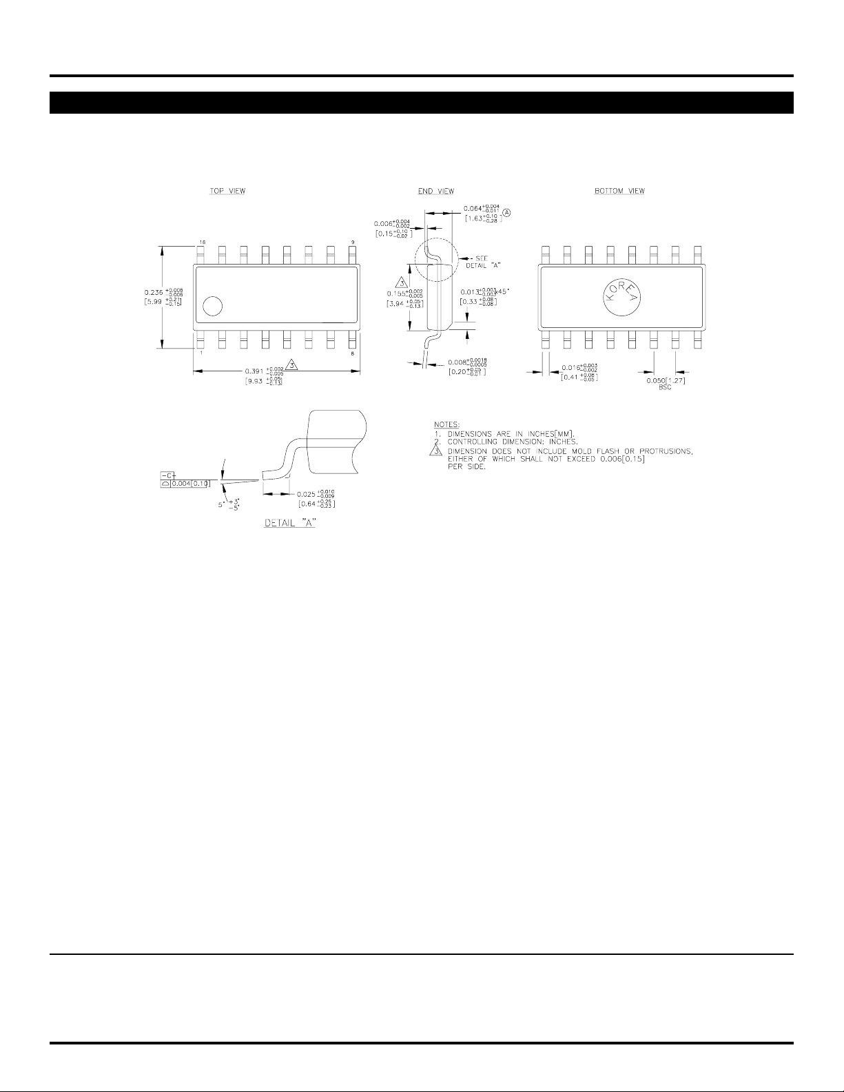
Micrel
16 LEAD SOIC .150" WIDE (Z16-2)
SY10EL16VA-VF
SY100EL16VA-VF
Rev. 02
MICREL-SYNERGY 3250 SCOTT BOULEVARD SANTA CLARA CA 95054 USA
TEL + 1 (408) 980-9191 FAX + 1 (408) 914-7878 WEB http://www.micrel.com
This information is believed to be accurate and reliable, however no responsibility is assumed by Micrel for its use nor for any infringement of patents or
other rights of third parties resulting from its use. No license is granted by implication or otherwise under any patent or patent right of Micrel Inc.
© 2000 Micrel Incorporated
9
 Loading...