

Page 1
STP100NF04
STB100NF04, STB100NF04-1
N-CHANNEL 40V - 0.0043Ω - 120A TO-220/D2PAK/I2PAK
STripFET™ II POWER MOSFET
AUTOMOTIVE SPECIFIC
TYPE V
STP100NF0 4
STB100NF0 4
STB100NF0 4-1
■ TYPICAL R
■ STANDARD THRESHOLD DRIVE
■ 100% AVALANCHE TESTED
DSS
40 V
40 V
40 V
(on) = 0.0043 Ω
DS
R
DS(on)
< 0.0046 Ω
< 0.0046 Ω
<0.0046 Ω
I
D
120 A
120 A
120 A
Pw
300 W
300 W
300 W
DESCRIPTION
This Power Mosfet is the latest development of ST-
Microelectronics unique “Single Feature Size
™”
strip-based process. The res ulting transistor sh ows
extremely high packing density for low on-resistance, rugged avalanche characteristics and less
critical alignment steps therefore a remarkable manufacturing reproducibility.
APPLICATIONS
■ HIGH CURRENT, HIGH SWITCHING SPEED
■ MOTOR CONTROL, AUDIO AMPLIFIERS
■ DC-DC & DC-AC CONVERTERS
■ SOLENOID AND RELAY DRIVERS
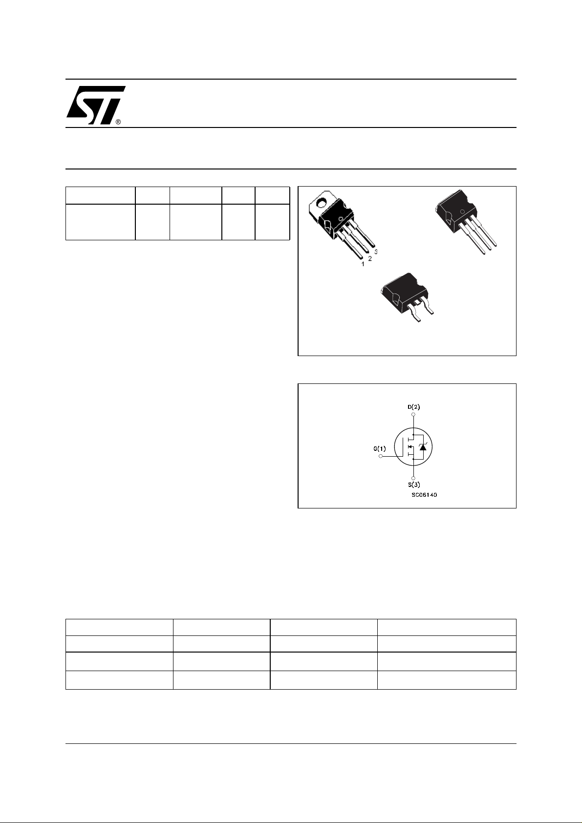
TO-220
1
D2PAK
I2PAK
3
INTERNAL SCHEMATIC DIAGRAM
3
2
1
ORDERING INFORMATION
SALES TYPE MARKING PACKAGE PACKAGING
STP100NF04 P100NF04 TO-220 TUBE
STB100NF04T4 B100NF04
STB100NF04-1
February 2002
B100NF04
2
D
PAK
2
I
PAK
TAPE & REEL
TUBE
1/15
Page 2
STP100NF04, STB100NF04, STB100NF04-1
ABSOLUTE MAXIMUM RATINGS
Symbol Parameter Value Unit
V
DS
V
DGR
V
GS
I
(#) Drain Current (continuos) at TC = 25°C
D
I
D
I
DM
P
TOT
dv/dt (1) Peak Diode Recovery voltage slope 6 V/ns
E
AS
T
j
T
stg
(l) Pulse wi dth limited by saf e operating area
(1) I
≤120A, di/dt ≤ 300A/µs, VDD ≤ V
SD
(2) Starting Tj = 25°C, Id = 60A, VDD=30 V
(#) Current Limited by Package
THERMA L D ATA
Rthj-case Thermal Resistance Junction-case Max 0.5 °C/W
Rthj-pcb Thermal Resistance Junction-pcb Max See Curve on page 6 °C/W
Rthj-amb Thermal Resistance Junction-ambient (Free air) Max 62.5 °C/W
T
l
Drain-source Voltage (VGS = 0)
Drain-gate Voltage (RGS = 20 kΩ)
40 V
40 V
Gate- source Voltage ± 20 V
120 A
Drain Current (continuos) at TC = 100°C
(l)
Drain Current (pulsed) 480 A
Total Dissipation at TC = 25°C
120 A
300 W
Derating Factor 2 W/°C
(2)
Single Pulse Avalanche Energy 1.2 J
Operating Junction Temperature
-55 to 175 °C
Storage Temperature
, Tj ≤ T
(BR)DSS
Maximum Lead Temperature For Soldering Purpose
JMAX.
TO-220 / I
2
PAK / D2PAK
300 °C
ELECTRICAL CHARACTERISTICS (TCASE =25°C UNLESS OTHERWISE SPECIFIED)
ON/OFF
Symbol Parameter Test Conditions Min. Typ. Max. Unit
V
(BR)DSS
I
DSS
I
GSS
V
GS(th)
R
DS(on)
2/15
Drain-source
Breakdown Voltage
Zero Gate Voltage
Drain Current (V
GS
= 0)
Gate-body Leakage
Current (V
DS
= 0)
Gate Threshold Voltage
Static Drain-source On
Resistance
ID = 250 µA, VGS = 0 40 V
V
= Max Rating
DS
V
= Max Rating, TC = 125 °C
DS
V
= ± 20V ±100 nA
GS
V
= VGS, ID = 250µA
DS
24V
1
10
VGS = 10V, ID = 50 A 0.0043 0.0046 Ω
µA
µA
Page 3

STP100NF04, STB100NF04, STB100NF04-1
ELECTRICAL CHARACTERISTICS (CONTINUED)
DYNAMIC
Symbol Parameter Test Conditions Min. Typ. Max. Unit
(1) Forward Transconductance VDS = 15 V, ID= 50 A 150 S
g
fs
C
iss
C
oss
C
rss
SWITCHING ON
Symbol Parameter Test Conditions Min. Typ. Max. Unit
t
d(on)
t
r
Q
g
Q
gs
Q
gd
SWITCHING OFF
Symbol Parameter Test Conditions Min. Typ. Max. Unit
t
d(off)
t
f
Input Capacitance
Output Capacitance
Reverse Transfer
Capacitance
Turn-on Delay Time
Rise Time
Total Gate Charge
Gate-Source Charge
Gate-Drain Charge
Turn-off Delay Time
Fall Time
= 25V, f = 1 MHz, VGS = 0 5100
V
DS
VDD = 20 V, ID = 60 A
R
= 4.7Ω VGS = 10 V
G
(Resistive Load see, Figure 3)
= 32V, ID = 120 A,
V
DD
VGS = 10V
(see, Figure 4)
VDD = 20 V, ID = 60 A
RG=4.7Ω VGS = 10 V
(Resistive Load see, Figure 3)
1300
160
35
220
110
35
35
80
50
150
pF
pF
pF
ns
ns
nC
nC
nC
ns
ns
SOURCE DRAIN DIODE
Symbol Parameter Test Conditions Min. Typ. Max. Unit
I
SD
I
SDM
VSD (1)
t
rr
Q
rr
I
RRM
Note: 1. Pulsed: Pu l se duration = 300 µs, duty c yc l e 1.5 %.
2. Pulse width li mited by safe operating area.
Source-drain Current
(2)
Source-drain Current (pulsed)
Forward On Voltage
Reverse Recovery Time
Reverse Recovery Charge
Reverse Recovery Current
ISD = 120 A, VGS = 0
I
SD
VDD = 20V, Tj = 150°C
(see test circuit, Figure 5)
= 120 A, di/dt = 100A/µs
75
185
5
120
480
1.3 V
A
A
ns
nC
A
3/15
Page 4
STP100NF04, STB100NF04, STB100NF04-1
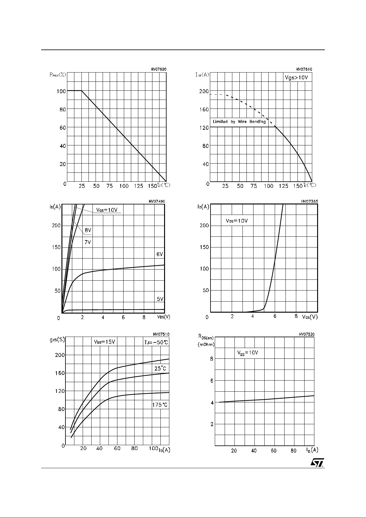
Power Derating vs Tc
Output Characteristics
Max Id Current vs Tc
Transfer Characteristics
Transconductance
4/15
Static Drain-source On Resistance
Page 5

STP100NF04, STB100NF04, STB100NF04-1
Gate Charge vs Gate-source Voltage
Normalized Gate Thereshold Voltage vs Temp.
Capacitance Variations
Normalized On Resistance vs Temperatur e
Source-drain Diode Forward Characteristics
Normalized Breakdown voltage vs Temperature
5/15
Page 6

STP100NF04, STB100NF04, STB100NF04-1
Thermal Resistance Rthj-a vs PCB Copper Area
Safe Operating Area
Max Power Dissipation vs PCB Copper Area
Thermal Impedance
6/15
Page 7

STP100NF04, STB100NF04, STB100NF04-1
Allowable Iav vs. Time in Avalanche
The previous curve gives the safe operating area for unclamped inductive loads, single pulse or repetitive,
under the following conditions:
P
E
= 0.5 * (1.3 * BV
D(AVE)
= P
AS(AR)
D(AVE)
* t
AV
DSS
* IAV)
Where:
is the Allowable Current in Avalanche
I
AV
P
t
AV
is the Average Power Dissipation in Avalanche (Single Pulse)
D(AVE)
is the Time in Avalanche
To derate above 25 °C, at fixed I
I
AV
Where:
= K * R
Z
th
is the value coming from Normalized Thermal Response at fixed pulse width equal to TAV.
th
the following equation must be applied:
AV,
= 2 * (T
jmax
- T
) / (1.3 * BV
CASE
DSS
* Zth)
7/15
Page 8

STP100NF04, STB100NF04, STB100NF04-1
SPICE THERMAL MODEL
Parameter Node Value
CTHERM1 5 - 4 0.011
CTHERM2 4 - 3 0.0012
CTHERM3 3 - 2 0.05
CTHERM4 2 - 1 0.1
RTHERM1 5 - 4 0.09
RTHERM2 4 - 3 0.02
RTHERM3 3 - 2 0.11
RTHERM4 2 - 1 0.17
8/15
Page 9

STP100NF04, STB100NF04, STB100NF04-1
Fig. 1: Unclamped Inductive Load Test Circuit
Fig. 3: Switching Times Test Circuit For
Resistive Load
Fig. 2: Unclamped Inductive Waveform
Fig. 3.1: Inductive Load Switching And Diode Re-
covery Times Waveform
Fig. 4: Gate Charge test Circuit
Fig. 4.1: Gate Charge test Waveform
9/15
Page 10

STP100NF04, STB100NF04, STB100NF04-1
Fig. 5: Test Circuit For Diode Recovery Times
Fig. 5.1: Diode Recovery Times Waveform
10/15
Page 11

STP100NF04, STB100NF04, STB100NF04-1
E
TO-220 MECHANICAL DATA
DIM.
A 4.40 4.60 0.173 0.181
C 1.23 1.32 0.048 0.051
D 2.40 2.72 0.094 0.107
D1 1.27 0.050
E 0.49 0.70 0.019 0.027
F 0.61 0.88 0.024 0.034
F1 1.14 1.70 0.044 0.067
F2 1.14 1.70 0.044 0.067
G 4.95 5.15 0.194 0.203
G1 2.4 2.7 0.094 0.106
H2 10.0 10.40 0.393 0.409
L2 16.4 0.645
L4 13.0 14.0 0.511 0.551
L5 2.65 2.95 0.104 0.116
L6 15.25 15.75 0.600 0.620
L7 6.2 6.6 0.244 0.260
L9 3.5 3.93 0.137 0.154
DIA. 3.75 3.85 0.147 0.151
MIN. TYP. MAX. MIN. TYP. MAX.
mm inch
A
C
D
L5
Dia.
L7
D1
L6
L2
L9
F1
G1
F
H2
G
F2
L4
P011C
11/15
Page 12

STP100NF04, STB100NF04, STB100NF04-1
2
D
PAK MECHANICAL DATA
DIM.
MIN. TYP MAX. MIN. TYP. MAX.
A 4.4 4.6 0.173 0.181
A1 2.49 2.69 0.098 0.106
A2 0.03 0.23 0.001 0.009
B 0.7 0.93 0.027 0.036
B2 1.14 1.7 0.044 0.067
C 0.45 0.6 0.017 0.023
C2 1.23 1.36 0.048 0.053
D 8.95 9.35 0.352 0.368
D1 8 0.315
E 10 10.4 0.393
E1 8.5 0.334
G 4.88 5.28 0.192 0.208
L 15 15.85 0.590 0.625
L2 1.27 1.4 0.050 0.055
L3 1.4 1.75 0.055 0.068
mm. inch
M 2.4 3.2 0.094 0.126
R 0.4 0.015
V2 0º8º
3
12/15
1
Page 13

STP100NF04, STB100NF04, STB100NF04-1
TO-262 (I2PAK) MECHANICAL DATA
DIM.
MIN. TYP. MAX. MIN. TYP. MAX.
A 4.4 4.6 0.173 0.181
A1 2.49 2.69 0.098 0.106
B 0.7 0.93 0.027 0.036
B2 1.14 1.7 0.044 0.067
C 0.45 0.6 0.017 0.023
C2 1.23 1.36 0.048 0.053
D 8.95 9.35 0.352 0.368
e 2.4 2.7 0.094 0.106
E 10 10.4 0.393 0.409
L 13.1 13.6 0.515 0.531
L1 3.48 3.78 0.137 0.149
L2 1.27 1.4 0.050 0.055
mm inch
C
A
A1
C2
B2
B
e
E
L1
L2
D
L
P011P5/E
13/15
Page 14

STP100NF04, STB100NF04, STB100NF04-1
D2PAK FOOTPRINT
TAPE AND REEL SHIPMENT (suffix ”T4”)*
TUBE SHIPMENT (no suffix)*
REEL MECHANICAL DATA
DIM.
A 330 12.992
B 1.5 0.059
C 12.8 13.2 0.504 0.520
D 20.2 0795
G 24.4 26.4 0.960 1.039
N 100 3.937
T 30.4 1.197
mm inch
MIN. MAX. MIN. MAX.
TAPE MECHANICAL DATA
DIM.
A0 10.5 10.7 0.413 0.421
B0 15.7 15.9 0.618 0.626
D 1.5 1.6 0.059 0.063
D1 1.59 1.61 0.062 0.063
E 1.65 1.85 0.065 0.073
F 11.4 11.6 0.449 0.456
K0 4.8 5.0 0.189 0.197
P0 3.9 4.1 0.153 0.161
P1 11.9 12.1 0.468 0.476
P2 1.9 2.1 0.075 0.082
R 50 1.574
T 0.25 0.35 0.0098 0.0137
W 23.7 24.3 0.933 0.956
* on sales type
14/15
mm inch
MIN. MAX. MIN. MAX.
BASE QTY BULK QTY
1000 1000
Page 15

STP100NF04, STB100NF04, STB100NF04-1
Information furnished is believed to be accurate and reliable. However, STMicroelectronics assumes no responsibility for the consequences
of use of such informa tion n or for an y infring ement of patent s or other rig hts of third part ies which may resu lt from its use . No l i cen se i s
granted by implication or otherwise under any patent or patent rights of STMicroelectronics. Specification mentioned in this publication are
subject to change without notice. This publication supersedes and replaces all information previously supplied. STMicroelectronics products
are not authorized for use as critical compo nents in life support devices or systems without express written approval of STMicroelectronics.
Australia - Brazil - China - Finland - France - Germany - Hong Kong - India - Italy - Japan - Malaysia - Malta - Morocco -
The ST logo is a trademark of STMicroelectronics
© 2000 STMicroelectronics – Printed in Italy – All Rights Reserved
STMicroelectronics GROUP OF COMPANIES
Singapore - Spain - Sweden - Switzerland - United Kingdom - U.S.A.
http://www.st.com
15/15
 Loading...