

Page 1
INTEGRATED CIRCUITS
SA9502
Dual-band, CDMA/AMPS
downconverter IC
Product specification
Supersedes data of 1998 Dec 10
IC17 Data Handbook
1999 Mar 19
Page 2
Philips Semiconductors Product specification
SA9502Dual-band, CDMA/AMPS downconverter IC
DESCRIPTION
The SA9502 integrates all the front end receive mixers necessary
for use in dual-band, triple-mode CDMA/AMPS cellular phone
handsets. There are three individual mixer blocks, each optimised
for high linearity with low power consumption for operation in one of
the following modes: High-band 1900MHz PCS CDMA, low-band
800MHz cellular CDMA or analog FM AMPS/TACS modes.
Additionally, the entire circuit can be powered down and put into
sleep mode, reducing the supply current to typically 12 µA. The
circuit has been designed in our advanced QUBiC2 BiCMOS
process with 20GHz f
.
T
FEATURES
•PCS and cellular downconverter mixers typical performance:
– PCS: Gain=1 1.1dB, NF=8.4dB, IIP3= +1.8dBm
– CDMA: Gain=1 1.3dB, NF=9.4dB, IIP3= +5.7dBm
– FM: Gain= 7.5dB, NF=10.5dB, IIP3= +6.2dBm
•Separate, selectable IF outputs to suit FM and CDMA bandwiths
•PCS mixer LO: direct or via internal frequency doubler
•Switchable wideband LO output buffer
•Low voltage operation down to 2.7V
•Low current consumption in “idle”/receive modes:
– PCS : 14.3mA @ 2.7V
– CDMA: 17.6mA @ 2.7V
– FM: 6.8mA @ 2.7V
•Low standby current in sleep mode, typically 12 µA
•TSSOP20 package
APPLICA TIONS
•800MHz analog FM and CDMA digital receivers
•1900MHz PCS band CDMA digital recievers
•Supports dual-mode and triple-mode operation
•Digital mobile communications equipment
•Portable, low power radio equipment
ORDERING INFORMATION
EXTENDED
TYPE NUMBER
SA9502DH 20 TSSOP Plastic thin shrink small outline package; body 6.5 x 4.4 x 1.1 mm SOT360-1
PINS PIN POSITION MATERIAL CODE
PACKAGE
1999 Mar 19 853–2135 21064
2
Page 3
Philips Semiconductors Product specification
SA9502Dual-band, CDMA/AMPS downconverter IC
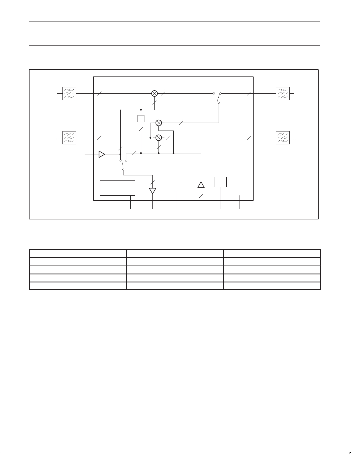
BLOCK DIAGRAM
RX BPF
Fo = 1960 MHz
BW = 60 MHz
PCS_in
RX BPF
Fo = 881.5MHz
BW = 45 MHz
Cell_in
PCS LO
2
×2
2
1
1
1
CELLPCS
MODE
SELECT
LOGIC
CDMA/FM PCS/CELL LO OUT LO BUFFER
2
2
2
2
2
1
ENABLE
Figure 1. Block Diagram
1
CEL
LO IN
PCS
CELL
SA9502
BIAS
CTRL
V
CC
2
2
PWR ON/OFF
CDMA IF BPF
Fo = 85.38MHz
BW = 1.23MHz
CDMA_Out
FM_Out
FM IF BPF
Fo = 85.38MHz
BW = 30kHz
SR01718
Table 1. Mode Selection Summary
PCS/CEL (Pin 6) CDMA/FM/LO doubler (Pin 17) MODE
low low Cellular FM
low high Cellular CDMA
high low CDMA PCS, direct LO in
high high CDMA PCS, LO via frequency doubler
1999 Mar 19
3
Page 4

Philips Semiconductors Product specification
SA9502Dual-band, CDMA/AMPS downconverter IC
PIN CONFIGURATION
1
2
FM IFB
3
GND
4
PCS RF
CEL RF
GND
V
5
6
7
8
9
CC
PCS RFB
PCS/CEL SEL
PWR ON/OFF
Figure 2. Pin Configuration
20FM IF
19
18
17
16
15
14
13
12
11
SR01760
CDMA IF
CDMA IFB
GND
CDMA/FM SEL
CEL LO IN
GND
PCS LO
LO BUFFER ENABLE
GND
LO OUT10
PIN DESCRIPTION
PIN SYMBOL DESCRIPTION
1 FM IF Non-inverting FM IF output
2 FM IFB Inverting FM IF output
3 GND Analog ground
4 PCS RF non-inverting PCS RF input
5 PCS RFB Inverting PCS RF input
6 PCS/CEL SEL PCS and cellular band select
7 PWR ON/OFF Power enable
8 CEL RF Cellular RF input
9 GND Ground
10 V
CC
11 LO OUT LO output to synthesizer
12 GND Ground
13 LO BUFFER
ENABLE
14 PCS LO PCS mixer direct LO input
15 GND Ground
16 CEL LO Cellular LO input
17 CDMA/FM SEL CDMA and FM mode select in cellular
18 GND Ground
19 CDMA IFB Inverting CDMA IF output
20 CDMA IF Non-inverting CDMA IF output
Power supply
Logic signal which switches the LO
buffer output ON or OFF
band; LO direct or via frequency
doubler in PCS mode
FUNCTIONAL DESCRIPTION
Mode Selection Logic
The SA9502 downconverter IC has several modes of operation for
which the selection logic is summarized in Table 1 and defined in
detail in Table 2. Different mode selections require different portions
of the circuit to be active. It should be noted that only the states
specified in Table 2 are valid selections for operation.
Local Oscillator Section
Local oscillator drive for the mixers is provided through single ended
inputs on either pin 16 (CEL LO) or pin 14 (PCS LO). The LO signal
has to be AC-coupled into the circuit and needs to be externally
matched. Inside the circuit, the cellular band LO signal is amplified
and buffered to drive: Either the cellular CDMA mixer or FM mixer
or the frequency doubler for the PCS mixer LO and additionally the
LO output buffer. The mode selection summary in Table 1 shows the
logic to apply to pins 6 and 17 to choose one of four possible
modes. The LO output buffer can be programmed on or off via LO
Buffer Enable (Pin 13). The LO output buffer’s frequency is the
same as that used by the mixers.
Cellular and PCS Mixers
The SA9502 has one single ended cellular band RF input which
feeds either the cellular CDMA mixer or the cellular FM mixer
circuits. Each mixer is optimized to meet cellular band CDMA or
analog FM requirements. The cellular FM mixer has its own
dedicated differential output on pins 1 and 2 which should to be
externally matched to the FM IF SAW filter . The cellular CDMA
mixer shares the same output pins with the CDMA PCS mixer.
Selection between these two mixers is via pin 6 (PCS/CEL) and as
the two mixers are never on at the same time, it allows a common
CDMA SAW filter to be used for both bands. The CDMA PCS mixer
has a differential RF input which should be used with an external
balun matching circuit. To avoid upsetting the internal biasing, the
RF inputs at both cellular and PCS band mixers should be
AC-coupled in. The CDMA and FM IF mixer outputs are of the open
collector type. So, they should be biased to the supply voltage V
with external tuning inductors which can also serve in the matching
of the IF SAW filter.
CC
1999 Mar 19
4
Page 5
Philips Semiconductors Product specification
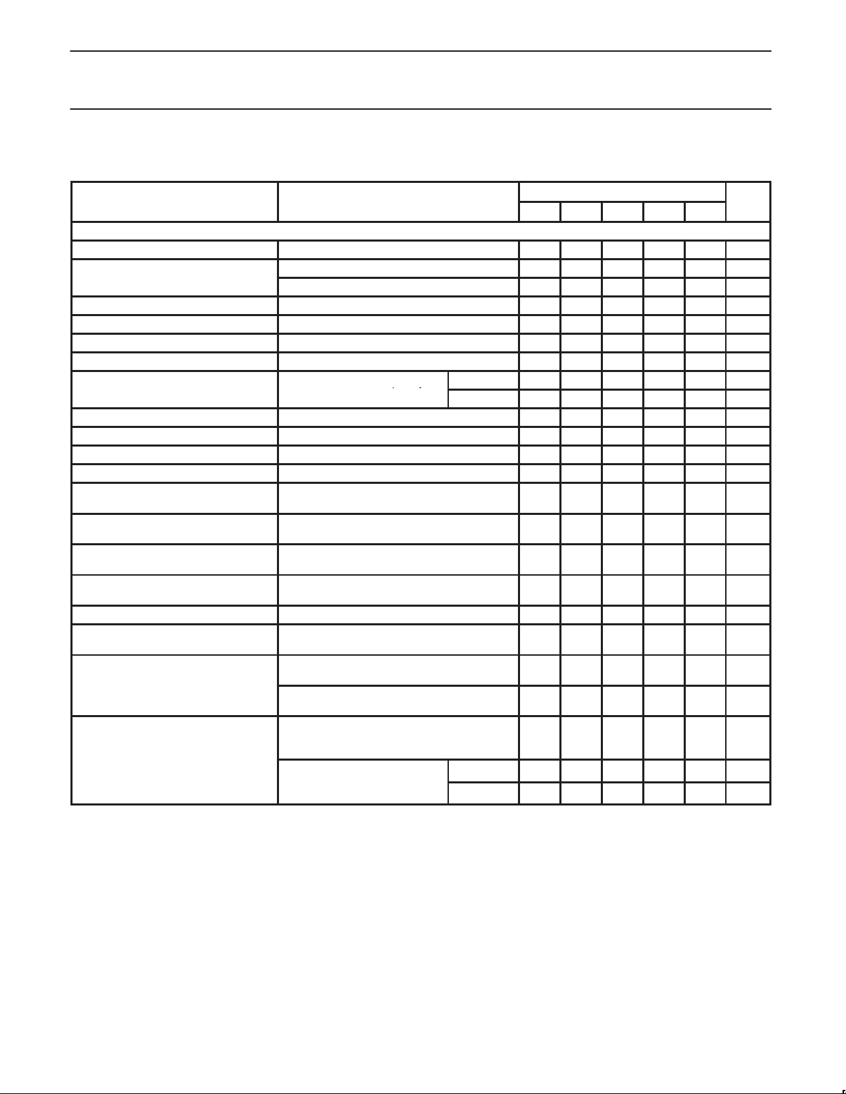
PARAMETER
TEST CONDITIONS
ÁÁÁÁ
UNITS
ÁÁÁÁ
ÁÁÁÁ
Logic i
ÁÁÁÁ
ÁÁÁÁ
ÁÁÁÁ
SA9502Dual-band, CDMA/AMPS downconverter IC
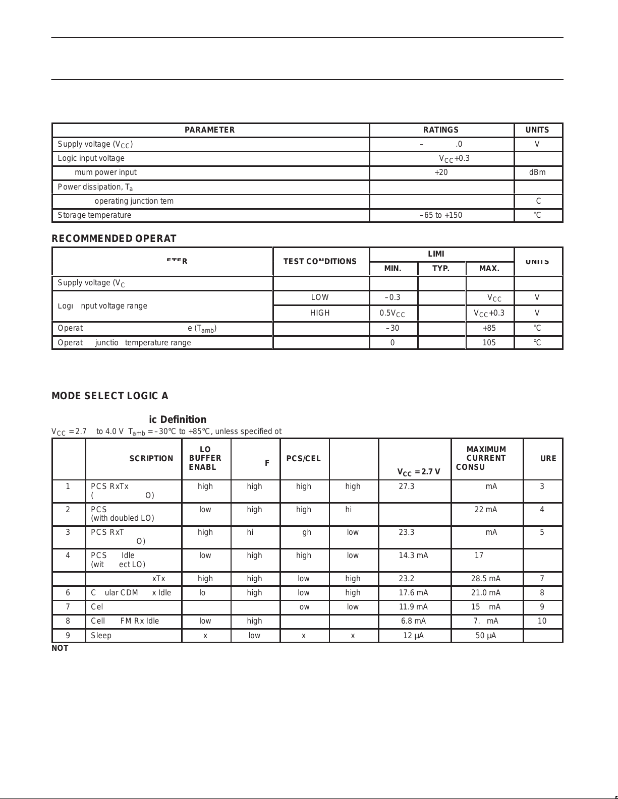
ABSOLUTE MAXIMUM RATINGS
PARAMETER
Supply voltage (VCC)
Logic input voltage
Maximum power input
Power dissipation, T
amb
=25°C
Maximum operating junction temperature
Storage temperature
RECOMMENDED OPERATING CONDITIONS
Supply voltage (VCC)
nput voltage range
Operating ambient temperature range (T
Operating junction temperature range
amb
)
LOW
HIGH
MIN.
2.7
–0.3
0.5V
–30
0
RATINGS
–0.3 to +6.0
–0.3 to VCC+0.3
–65 to +150
LIMITS
CC
+20
800
150
TYP.
3.0
MAX.
4.0
0.2V
CC
VCC+0.3
+85
105
UNITS
V
V
dBm
mW
°C
°C
V
V
V
°C
°C
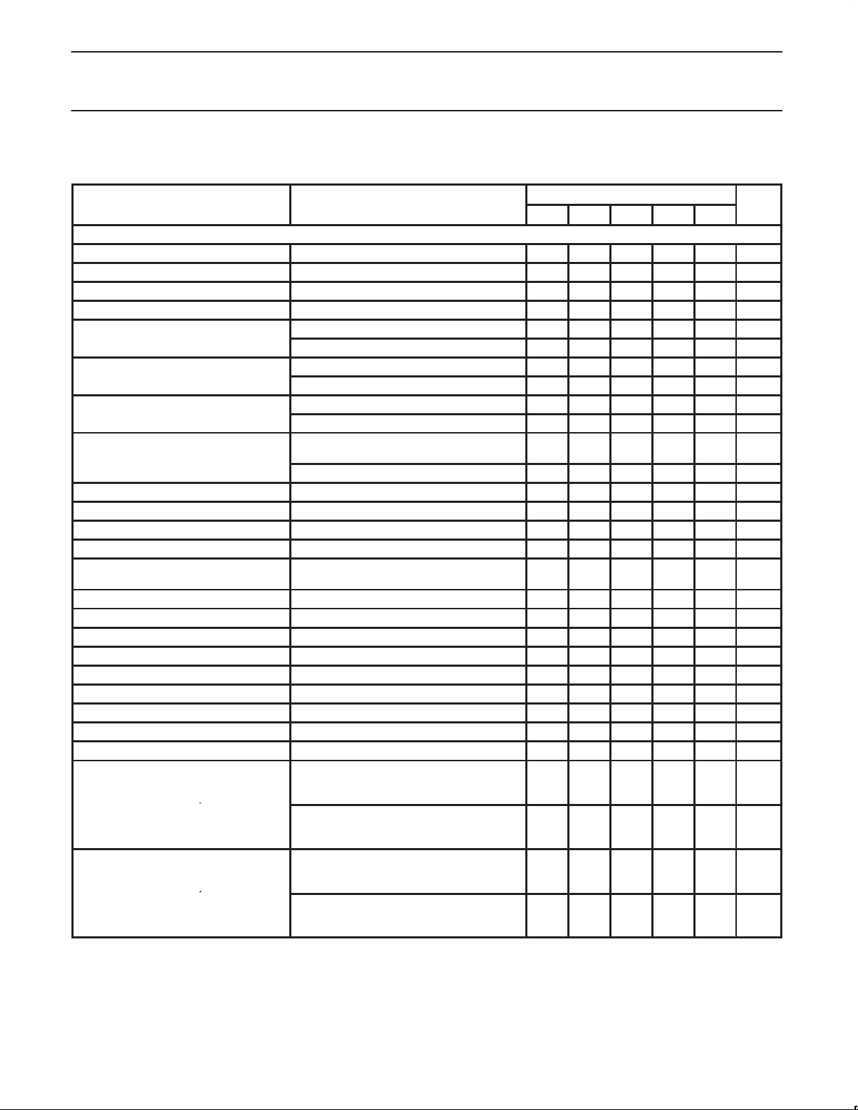
MODE SELECT LOGIC AND DC CHARACTERISTICS
Table 2. Mode Logic Definition
VCC = 2.7 V to 4.0 V; T
MODE
MODE DESCRIPTION
1 PCS RxTx
(with doubled LO)
2 PCS Idle
(with doubled LO)
3 PCS RxTx
(with direct LO)
4 PCS Rx Idle
(with direct LO)
5 Cellular CDMA RxTx high high low high 23.2 mA 28.5 mA 7
6 Cellular CDMA Rx Idle low high low high 17.6 mA 21.0 mA 8
7 Cellular FM RxTx high high low low 1 1.9 mA 15.5 mA 9
8 Cellular FM Rx Idle low high low low 6.8 mA 7.8 mA 10
9 Sleep x low x x 12 µA 50 µA
NOTE:
x = Don’t care
= –30°C to +85°C, unless specified otherwise.
amb
LO
BUFFER
ENABLE
POWER
ON/OFF
high high high high 27.3 mA 33 mA 3
low high high high 18.4 mA 22 mA 4
high high high low 23.3 mA 28 mA 5
low high high low 14.3 mA 17 mA 6
PCS/CEL CDMA/FM
TYPICAL
CURRENT
CONSUMPTION
= 2.7 V
@ V
CC
MAXIMUM
CURRENT
CONSUMPTION
FIGURE
1999 Mar 19
5
Page 6
Philips Semiconductors Product specification
PARAMETER
TEST CONDITIONS
UNITS
IF output load impedance
Conversion gain
Noise figure
j
j
SA9502Dual-band, CDMA/AMPS downconverter IC
AC ELECTRICAL CHARACTERISTICS
VCC = 2.7V; T
Cellular Band Downconverter
RF input frequency range 869 894 MHz
LO input frequency range 950 1030 MHz
IF output frequency range (CDMA) 50 300 MHz
IF output frequency range (FM) 50 300 MHz
Input IP3
RF input return loss ZS = 50Ω 11.0 dB
LO input return loss ZS = 50Ω 10.0 dB
LO output return loss ZS = 50Ω 8.0 dB
LO input power range –6.0 –3.0 0.0 dBm
LO output power range
LO (input and output) to RF leakage Single-ended in, single-ended out –34.5 –31.5 dBm
LO (output) to IF leakage (CDMA) Single-ended in, differential out –33.6 –29.0 dBm
LO (output) to IF leakage (FM) Single-ended in, differential out –20.0 –17.5 dBm
LO (input) to IF leakage (CDMA) Single-ended in, differential out –27.7 –26.5 dBm
LO (input) to IF leakage (FM) Single-ended in, differential out –18.5 –17.8 dBm
RF to LO (input) isolation Single-ended in, single-ended out 30 32.8 dB
RF to IF isolation (CDMA) Single-ended in, differential out 17 17.7 dB
RF to IF isolation (FM) Single-ended in, differential out 6 8.2 dB
LO output to LO input isolation Single-ended in, single-ended out 26.5 33 dB
Spurious response rejection
(CDMA mode)
Spurious response rejection
(FM mode)
= +25°C; Plo = –3 dBm, fIF = 85.40 MHz and measured on Philips demonstration board; unless specified otherwise.
amb
MIN. –3σ TYP. +3σ MAX.
p
p
CDMA, differential 1000 Ω
FM, single-ended, with ext. balun 850 Ω
CDMA 10.7 11.3 11.9 dB
FM 7.0 7.5 8.0 dB
CDMA mode, SSB 9.4 10.0 dB
FM mode, SSB 10.5 10.7 dB
CDMA mode, tone spacing = 900 kHz and
1.7 MHz
FM mode, tone spacing = 60 kHz 5.3 6.2 dBm
ZL = 50Ω, single LO out
with LO buffer on (Pin 13 = High)
With Tx band interferer at LO input port or
LO buffer output port of –40 dBm max and
with Pint = –31 dBm in Rx band.
With Tx band interferer at RF input port of
–40 dBm max and with Pint = –31 dBm in
Rx band.
With Tx band interferer at LO input port or
LO buffer output port of –40 dBm max and
with Pint = –31 dBm in Rx band.
With Tx band interferer at RF input port of
–40 dBm max and with Pint = –31 dBm in
Rx band.
4.8 5.7 dBm
–7.5 –5.0 –3.0 dBm
43 44 dB
59 61 dB
43 44 dB
55 56 dB
1999 Mar 19
6
Page 7
Philips Semiconductors Product specification
PARAMETER
TEST CONDITIONS
UNITS
LO input frequency range
Input IP3
IF
,qy
1/2 IF supurious rejection
Spurious response rejection
in ut ort of –40 dBm max and
SA9502Dual-band, CDMA/AMPS downconverter IC
AC ELECTRICAL CHARACTERISTICS (continued)
VCC = 2.7V; T
PCS Downconverter
RF input frequency range 1810 1990 MHz
IF output frequency range 50 300 MHz
IF output load impedance Differential 1000 Ω
Conversion gain @ fIF, over RF/LO frequency ranges 10.5 11.1 11.7 dB
Noise figure @ fIF, over RF/LO frequency ranges, SSB 8.4 9.3 dB
p
RF input return loss ZS = 50Ω, with external balun 7.5 dB
LO input return loss ZS = 50Ω 10 dB
LO output return loss ZS = 50Ω, single LO out 8 dB
LO input power range –6 –3 0 dBm
LO output power range
LO (input and output) to RF leakage
LO (input and output) to IF leakage
RF to LO (input) isolation
RF to IF isolation Single-ended in, dif ferential out 32 40 dB
LO output to LO input isolation
p
= +25°C; Plo = –3 dBm, fIF = 85.40 MHz and measured on Philips demonstration board; unless specified otherwise.
amb
MIN –3σ TYP. +3σ MAX.
p
p
With doubler 860 1050 MHz
Direct PCS LO 1720 2200 MHz
@ fIF, over RF/LO frequency
ranges at 25°C @ VCC = 3.6V
ZL = 50Ω, single LO out with LO buffer on
(Pin 13 = High)
Single-ended in, single-ended out,
with and without doubler
Single-ended in, differential out,
with and without doubler
Single-ended in, single-ended out,
with and without doubler
Single-ended in, single-ended out,
with doubler
1/2 IF spur, fIF = 85.4 MHz/111.38 MHz,
with doubler, P
= –30 dBm at RF input.
int
1/2 IF spur, fIF = 85.4 MHz/111.38 MHz,
without doubler, P
= –30 dBm at RF input.
int
direct LO 0.5 1.8 dBm
doubled LO 0.1 1.2 dBm
–10.0 –8.5 –7 dBm
–56 –47 dBm
–43 –39 dBm
44 46 dB
30 31 dB
42 46 dB
68 76 dB
With Tx band interferer at LO input port or LO
buffer output port of –40 dBm max and with
= –21 dBm in Rx band.
P
p
int
With Tx band interferer at RF
p
p
with P
= –21 dBm in Rx band. doubled LO 53 61 dB
int
direct LO 59 64 dB
43 44 dB
1999 Mar 19
7
Page 8
Philips Semiconductors Product specification
SA9502Dual-band, CDMA/AMPS downconverter IC
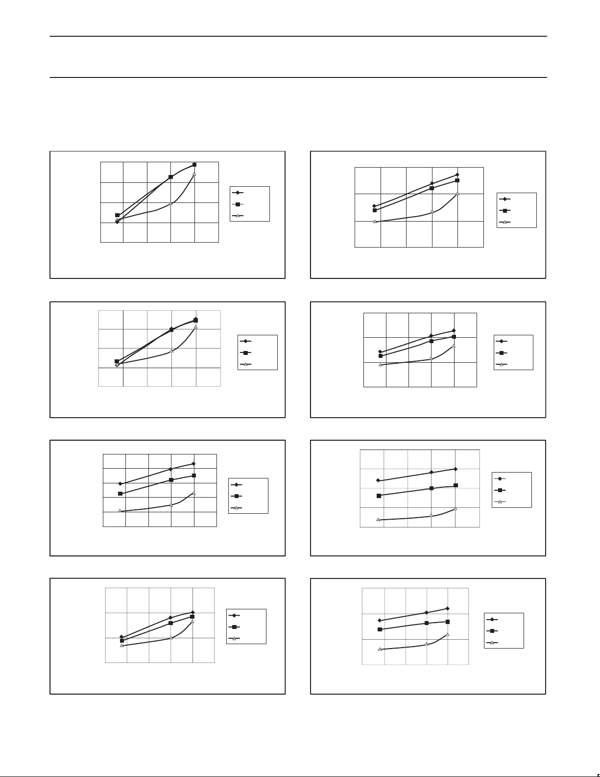
PERFORMANCE CHARACTERISTICS
DC Current Consumption
30.0
29.0
28.0
27.0
CURRENT (mA)
26.0
2.4 2.8 3.2 3.6 4.0 4.4
VCC (V)
SR01825
Figure 3. PCS RxTx (with doubled LO out) current
26.0
25.0
24.0
23.0
CURRENT (mA)
22.0
2.4 2.8 3.2 3.6 4 4.4
VCC (V)
Figure 5. PCS RxTx current
–30°C
+25°C
+85°C
–30°C
+25°C
+85°C
SR01827
20.0
19.0
18.0
CURRENT (mA)
17.0
2.4 2.8 3.2 3.6 4 4.4
VCC (V)
Figure 4. PCS Idle (with doubled LO out) current
16.0
15.0
14.0
CURRENT (mA)
13.0
2.4 2.8 3.2 3.6 4 4.4
(V)
V
CC
Figure 6. PCS Rx Idle current
–30°C
+25°C
+85°C
SR01826
–30°C
+25°C
+85°C
SR01828
26.0
25.0
24.0
23.0
CURRENT (mA)
22.0
21.0
2.4 2.8 3.2 3.6 4 4.4
VCC (V)
Figure 7. Cellular CDMA RxTx current
14.0
13.0
12.0
CURRENT (mA)
11.0
2.4 2.8 3.2 3.6 4 4.4
(V)
V
CC
Figure 9. Cellular FM RxTx current
–30°C
+25°C
+85°C
SR01829
–30°C
+25°C
+85°C
SR01831
20.0
19.0
18.0
17.0
CURRENT (mA)
16.0
2.4 2.8 3.2 3.6 4 4.4
VCC (V)
Figure 8. Cellular CDMA Rx Idle current
7.5
7.0
6.5
CURRENT (mA)
6.0
2.4 2.8 3.2 3.6 4 4.4
VCC (V)
Figure 10. Cellular FM Rx Idle current
–30°C
+25°C
+85°C
SR01830
–30°C
+25°C
+85°C
SR01832
1999 Mar 19
8
Page 9

Philips Semiconductors Product specification
SA9502Dual-band, CDMA/AMPS downconverter IC
PERFORMANCE CHARACTERISTICS
Mixer Noise Figure
Noise Figure vs. Temperature
VCC = 3.6V, Cellular RF Freq. = 880 MHz
11.2
10.8
10.4
10.0
9.6
NOISE FIGURE (dB)
9.2
8.8
–35 –15 5 25 45 65 85 105
TEMPERATURE (°C)
Figure 11.
Noise Figure vs. Temperature
VCC = 3.6V, PCS RF Freq. = 1960 MHz
12.0
10.0
8.0
6.0
4.0
NOISE FIGURE (dB)
2.0
CELLULAR
FM
CELLULAR
CDMA
SR01807
PCS,
DIRECT LO
PCS,
DOUBLED LO
Noise Figure vs. Cellular RF Frequency
VCC = 3.6V, T = 25°C
11.0
10.5
10.0
9.5
9.0
NOISE FIGURE (dB)
8.5
8.0
865 870 875 880 885 890 895
FREQUENCY (MHz)
Figure 12.
Noise Figure vs. PCS RF Frequency
VCC = 3.6V, T = 25°C
10.0
9.0
8.0
7.0
NOISE FIGURE (dB)
6.0
CELLULAR
FM
CELLULAR
CDMA
SR01808
PCS,
DIRECT LO
PCS,
DOUBLED LO
0
–35 –15 5 25 45 65 85 105
TEMPERATURE 〈°C)
Figure 13.
SR01809
5.0
1920 1940 1960 1980 2000
FREQUENCY (MHz)
Figure 14.
SR01810
1999 Mar 19
9
Page 10

Philips Semiconductors Product specification
SA9502Dual-band, CDMA/AMPS downconverter IC
PERFORMANCE CHARACTERISTICS
Conversion Gain – FM Mixer
Conversion Gain vs. Frequency
T = 25°C, Cellular FM
8.0
7.8
7.6
7.4
GAIN (dB)
7.2
2.7V
3.6V
Conversion Gain vs. Frequency
9.0
8.5
8.0
7.5
GAIN (dB)
7.0
6.5
VCC = 3.6V , Cellular FM
–30°C
+25°C
+85°C
7.0
860 870 880 890 900
FREQUENCY (MHz)
Figure 15.
Conversion Gain vs. LO Input Power
9.0
8.0
7.0
6.0
GAIN (dB)
5.0
4.0
3.0
–15 –12 –9 –6 –3 0
T = 25°C, Cellular FM
LO INPUT POWER (dBm)
Figure 17.
Conversion Gain vs. RF Input Power
T = 25°C, Cellular FM
7.5
7.0
GAIN (dB)
6.5
6.0
–35 –33 –31 –29 –27 –25
RF INPUT POWER (dBm)
Figure 19.
SR01811
VCC = 2.7V
= 3.6V
V
CC
VCC = 4.0V
SR01814
VCC = 2.7V
V
= 3.6V
CC
VCC = 4V
SR01833
6.0
870 880 890 900
860
FREQUENCY (MHz)
Figure 16.
Conversion Gain vs. LO Input Power
V
= 3.6V , Cellular FM
9.0
8.0
7.0
6.0
5.0
4.0
GAIN (dB)
3.0
2.0
1.0
0.0
CC
–15 –12 –9 –6 –3 0
LO INPUT POWER (dBm)
Figure 18.
Conversion Gain vs. RF Input Power
VCC = 3.6V , Cellular FM
7.8
7.4
7.0
6.6
GAIN (dB)
6.2
5.8
5.4
5.0
–35 –33 –31 –29 –27 –25
RF INPUT POWER (dBm)
Figure 20.
SR01811
–30°C
+25°C
+85°C
SR01815
–30°C
+25°C
+85°C
SR01834
1999 Mar 19
10
Page 11

Philips Semiconductors Product specification
SA9502Dual-band, CDMA/AMPS downconverter IC
PERFORMANCE CHARACTERISTICS
Conversion Gain – Cellular Band CDMA Mixer
Conversion Gain vs. Frequency
T = 25°C, Cellular CDMA
11.5
11.4
11.3
11.2
GAIN (dB)
11.1
11.0
865 870 875 880 885 890 895
FREQUENCY (MHz)
Figure 21.
2.7V
3.6V
SR01798
Conversion Gain vs. Frequency
VCC = 3.6V, Cellular CDMA
13.5
13.0
12.5
12.0
11.5
GAIN (dB)
11.0
10.5
10.0
9.5
870 880 890 900
860
FREQUENCY (MHz)
Figure 22.
–30°C
+25°C
+85°C
SR01799
Conversion Gain vs. LO Input Power
T = 25°C, Cellular CDMA
12.0
11.0
10.0
9.0
8.0
7.0
GAIN (dB)
6.0
5.0
4.0
3.0
2.0
–15 –12 –9 –6 –3 0
LO INPUT POWER (dBm)
Figure 23.
Conversion Gain vs. RF Input Power
T = 25°C, Cellular CDMA
12.0
11.0
10.0
GAIN (dB)
9.0
VCC = 2.7V
= 3.6V
V
CC
VCC = 4.0V
SR01803
VCC = 2.7V
V
= 3.6V
CC
VCC = 4.0V
Conversion Gain vs. LO Input Power
V
= 3.6V, Cellular CDMA
12.0
11.0
10.0
9.0
8.0
7.0
GAIN (dB)
6.0
5.0
4.0
3.0
2.0
CC
–15 –12 –9 –6 –3 0
LO INPUT POWER (dBm)
Figure 24.
Conversion Gain vs. RF Input Power
VCC = 3.6V, Cellular CDMA
12.0
11.0
10.0
GAIN (dB)
9.0
–30°C
+25°C
+85°C
SR01804
–30°C
+25°C
+85°C
1999 Mar 19
8.0
–35 –33 –31 –29 –27 –25
RF INPUT POWER (dBm)
Figure 25.
SR01806
8.0
–35 –33 –31 –29 –27 –25
RF INPUT POWER (dBm)
SR01805
Figure 26.
11
Page 12

Philips Semiconductors Product specification
SA9502Dual-band, CDMA/AMPS downconverter IC
PERFORMANCE CHARACTERISTICS
Conversion Gain – PCS Mixer
Conversion Gain vs. Frequency
12
T = 25°C, PCS, Doubled LO
Conversion Gain vs. Frequency
VCC = 3.6V, PCS, Doubled LO
13.5
11.5
11
GAIN (dB)
10.5
10
1920 1940 1960 1980 2000
FREQ. (MHz)
Figure 27.
Conversion Gain vs. LO Input Power
T = 25°C, PCS, Doubled LO
12.0
10.0
8.0
6.0
4.0
2.0
0.0
GAIN (dB)
–2.0
–4.0
–6.0
–8.0
–15
–12 –9 –6 –3 0
LO INPUT POWER (dBm)
Figure 29.
+2.7V
+3.6V
SR01835
VCC = +2.7°C
= +3.6°C
V
CC
VCC = +4°C
SR01837
12.5
11.5
10.5
GAIN (dB)
9.5
8.5
1920 1940 1960 1980 2000
FREQ. (MHz)
Figure 28.
Conversion Gain vs. LO Input Power
V
= 3.6V, PCS, Doubled LO
CC
12.0
10.0
8.0
6.0
4.0
2.0
0.0
GAIN (dB)
–2.0
–4.0
–6.0
–8.0
–15 –12 –9 –6 –3 0
LO INPUT POWER (dBm)
Figure 30.
–30°C
+25°C
+85°C
SR01836
–30°C
+25°C
+85°C
SR01838
11.5
11.0
10.5
GAIN (dB)
10.0
9.5
1999 Mar 19
Conversion Gain vs. RF Input Power
T = 25°C, PCS, Doubled LO
–35 –33 –31 –29 –27 –25
RF INPUT POWER (dBm)
Figure 31.
VCC = +2.7V
= +3.6V
V
CC
VCC = +4V
SR01839
12
Conversion Gain vs. RF Input Power
VCC = 3.6V, PCS, Doubled LO
11.5
11.0
10.5
10.0
GAIN (dB)
9.5
9.0
8.5
–35 –33 –31 –29 –27 –25
RF INPUT POWER (dBm)
Figure 32.
–30°C
+25°C
+85°C
SR01840
Page 13

Philips Semiconductors Product specification
SA9502Dual-band, CDMA/AMPS downconverter IC
Conversion Gain vs. Frequency
T = 25°C, PCS, Direct LO
12.0
11.5
11.0
GAIN (dB)
10.5
10.0
1920 1940 1960 1980 2000
FREQ. (MHz)
Figure 33.
Conversion Gain vs. LO Input Power
T = 25°C, PCS, Direct LO
12.0
11.0
10.0
9.0
GAIN (dB)
8.0
7.0
6.0
–15 –12 –9 –6 –3 0
LO INPUT POWER (dBm)
Figure 35.
VCC = +3.6 V
= +2.7 V
V
CC
SR01841
VCC = 2.7V
= 3.6V
V
CC
VCC = 4V
SR01843
Conversion Gain vs. Frequency
VCC = 3.6V, PCS, Direct LO
13.0
12.5
12.0
11.5
11.0
10.5
GAIN (dB)
10.0
9.5
9.0
1920 1940 1960 1980 2000
FREQ. (MHz)
Figure 34.
Conversion Gain vs. LO Input Power
VCC = 3.6V, PCS, Direct LO
12.0
11.0
10.0
9.0
8.0
7.0
GAIN (dB)
6.0
5.0
4.0
3.0
–15 –12 –9 –6 –3 0
LO INPUT POWER (dBm)
Figure 36.
–30°C
+25°C
+85°C
SR01842
–30°C
+25°C
+85°C
SR01844
GAIN (dB)
1999 Mar 19
Conversion Gain vs. RF Input Power
T = 25°C, PCS, Direct LO
12.0
11.0
10.0
9.0
8.0
–35 –33 –31 –29 –27 –25
RF INPUT POWER (dBm)
Figure 37.
VCC = 2.7V
= 3.6V
V
CC
VCC = 4V
SR01845
13
Conversion Gain vs. RF Input Power
V
= 3.6V, PCS, Direct LO
CC
12.0
11.0
10.0
GAIN (dB)
9.0
8.0
–35 –33 –31 –29 –27 –25
RF INPUT POWER (dBm)
Figure 38.
–30°C
+25°C
+85°C
SR01846
Page 14

Philips Semiconductors Product specification
SA9502Dual-band, CDMA/AMPS downconverter IC
PERFORMANCE CHARACTERISTICS
Input IP3
Input IP3 vs. Temperature
VCC = 3.6V, Cellular RF Freq: 880 MHz
T = 25°C, Cellular RF Freq: 880 MHz
Input IP3 vs. V
CC
8.5
8.0
7.5
7.0
6.5
6.0
5.5
5.0
INPUT IP3 (dBm)
4.5
4.0
–35 –15 5 25 45 65 85 105
TEMP (C)
Figure 39.
Input IP3 vs. Temperature
V
= 3.6V, PCS RF Freq: 1960 MHz
CC
2.5
2
1.5
1
0.5
INPUT IP3 (dBm)
0
–0.5
–35 –15 5 25 45 65 85 105
TEMP (C)
Figure 41.
CELL
CDMA
CELL
FM
SR01847
PCS
DIRECT LO
PCS
DOUBLED LO
SR01849
7.5
7.0
6.5
6.0
INPUT IP3 (dBm)
5.5
5.0
2.5 3 3.5 4
VCC (V)
Figure 40.
Input IP3 vs. V
T = 25°C, PCS RF Freq: 1960 MHz
2
1.6
1.2
0.8
INPUT IP3 (dBm)
0.4
0
2.5 3 3.5 4
(V)
V
CC
Figure 42.
CC
CELL FM
CELL CDMA
SR01848
PCS
DIRECT LO
PCS
DOUBLED LO
SR01850
8
7.5
7
6.5
INPUT IP3 (dBm)
6
5.5
865 870 875 880 885 890 895
1999 Mar 19
Input IP3 vs. Cellular RF Frequency
VCC = 3.6V, T = 25°C
FREQ. (MHz)
Figure 43.
CELL CDMA
CELL FM
SR01851
14
Input IP3 vs. PCS RF Frequency
VCC = 3.6V, T = 25°C
2.5
2
1.5
1
INPUT IP3 (dBm)
0.5
0
1920 1940 1960 1980 2000
FREQ (MHz)
Figure 44.
PCS
DIRECT LO
PCS
DOUBLED LO
SR01852
Page 15

Philips Semiconductors Product specification
SA9502Dual-band, CDMA/AMPS downconverter IC
PERFORMANCE CHARACTERISTICS
1: 128.87Ω
67.805Ω
1.5GHz
2: 152.73Ω
–22.836Ω
1.8GHz
3: 118.62Ω
1
2
4
3
–67.359Ω
2.0GHz
4: 75.051Ω
–69.055Ω
1.0476pF
2.2GHz
START: 1.40GHz
STOP: 2.65GHz
Figure 45. Typical S22 of LO Output for the PCS Band @ VCC = 3.6V
Table 3. Typical S-Parameter of PCS LO Output @ VCC = 3.6V
FREQUENCY (MHz) S22 <S22 (DEG)
1400 0.54 29.37
1450 0.54 25.04
1500 0.55 20.11
1550 0.54 15.16
1600 0.54 10.52
1650 0.54 6.32
1700 0.53 1.21
1750 0.52 –2.79
1800 0.51 –6.41
1850 0.52 –9.43
1900 0.52 –13.94
1950 0.53 –18.30
2000 0.53 –22.79
2050 0.53 –27.61
2100 0.53 –32.24
2150 0.52 –36.61
2200 0.52 –41.20
2250 0.51 –45.82
2300 0.50 –50.03
2350 0.49 –54.48
2400 0.47 –59.11
2450 0.46 –63.38
2500 0.43 –66.38
2550 0.42 –68.80
2600 0.41 –71.64
2650 0.41 –74.32
SR01779
1999 Mar 19
15
Page 16

Philips Semiconductors Product specification
SA9502Dual-band, CDMA/AMPS downconverter IC
1: 35.711Ω
–3.1914Ω
200.25MHz
4
3
2
1
2: 23.251Ω
18.894Ω
500MHz
3: 30.5Ω
50.623Ω
900MHz
4: 53.047Ω
77.758Ω
10.313nH
1.2GHz
START: 100MHz
STOP: 1.35GHz
Figure 46. T ypical S22 of LO Output for the Cellular Band @ VCC = 3.6V
Table 4. Typical S-Parameter of LO Output for Cellular Band @ VCC = 3.6V
FREQUENCY (MHz) S22 <S22 (DEG)
100 0.09 –143.49
150 0.13 –153.08
200 0.17 –165.13
250 0.21 –176.62
300 0.26 172.24
350 0.31 161.47
400 0.36 150.70
450 0.40 140.09
500 0.43 130.28
550 0.46 121.52
600 0.48 113.59
650 0.50 106.59
700 0.52 100.18
750 0.54 94.52
800 0.55 89.12
850 0.56 84.05
900 0.57 78.74
950 0.57 73.92
1000 0.58 69.23
1050 0.59 64.44
1100 0.59 59.62
1150 0.60 55.17
1200 0.60 50.70
1250 0.60 46.34
1300 0.61 42.11
1350 0.61 37.86
SR01780
1999 Mar 19
16
Page 17

Philips Semiconductors Product specification
Frequency (MHz)
SA9502Dual-band, CDMA/AMPS downconverter IC
1: 35.71 1Ω
–3.1914Ω
200.25MHz
2: 23.251Ω
18.894Ω
500MHz
3: 30.5Ω
50.623Ω
900MHz
1
2
3
4: 53.047Ω
77.758Ω
10.313nH
1.2GHz
START: 100MHz
STOP: 1.35GHz
4
SR01781
Figure 47. T ypical S22 of CDMA IF, CDMA IFB, FM IF and FM IFB Output @ VCC = 3.6V
Table 5. Typical S-Parameter of CDMA IF and CDMA IFB, FM IF and FM IFB Output @ 3.6V
CDMA IF and CDMA IFB Modes FM IF and FM IFB Modes
S22 <S22 (DEG) S22 <S22 (DEG)
20 0.99 –3.28 0.99 –3.47
40 0.99 –6.54 0.99 –6.84
60 0.99 –9.66 0.99 –10.15
80 0.98 –12.94 0.99 –13.58
100 0.98 –16.27 0.99 –17.02
120 0.98 –19.53 0.99 –20.40
140 0.98 –22.81 0.98 –23.76
160 0.98 –26.02 0.98 –27.01
180 0.98 –29.28 0.98 –30.48
200 0.98 –32.69 0.97 –33.94
220 0.97 –35.92 0.97 –37.22
240 0.97 –39.50 0.97 –40.78
260 0.96 –42.76 0.96 –44.19
280 0.96 –46.15 0.95 –47.55
300 0.96 –49.62 0.95 –51.00
320 0.96 –53.12 0.94 –54.46
340 0.95 –56.57 0.94 –57.83
360 0.95 –60.22 0.93 –61.32
380 0.95 –63.71 0.92 –64.61
400 0.94 –67.33 0.92 –68.11
420 0.94 –70.92 0.91 –71.43
440 0.93 –74.64 0.90 –74.72
460 0.93 –78.22 0.90 –78.22
480 0.93 –81.92 0.89 –81.58
500 0.92 –85.75 0.88 –84.90
520 0.91 –89.44 0.88 –88.28
1999 Mar 19
17
Page 18

Philips Semiconductors Product specification
SA9502Dual-band, CDMA/AMPS downconverter IC
1: 42.641Ω
–83.805Ω
1.5GHz
2: 30.84Ω
–66.172Ω
1.8GHz
3: 25.9Ω
–56.061Ω
1.4195pF
2.0GHz
4: 19.625Ω
–46.301Ω
2.2GHz
3
1
2
4
START: 1.40GHz
STOP: 2.65GHz
Figure 48. T ypcial S11 of PCS RF and PCS RFB Input @ VCC = 3.6V
Table 6. Typical S-Parameter of PCS RF and PCS RFB Input @ VCC = 3.6V
FREQUENCY (MHz) S11 <S11 (DEG)
1400 0.68 –48.65
1450 0.68 –50.83
1500 0.68 –52.86
1550 0.67 –55.14
1600 0.67 –57.35
1650 0.67 –59.59
1700 0.66 –62.09
1750 0.66 –64.21
1800 0.66 –66.78
1850 0.66 –69.35
1900 0.65 –71.92
1950 0.65 –74.58
2000 0.65 –76.86
2050 0.65 –79.82
2100 0.66 –82.80
2150 0.66 –85.95
2200 0.66 –89.71
2250 0.66 –93.52
2300 0.66 –97.51
2350 0.65 –101.41
2400 0.63 –105.60
2450 0.61 –109.66
2500 0.59 –114.00
2550 0.56 –117.05
2600 0.53 –119.59
2650 0.50 –120.82
SR01782
1999 Mar 19
18
Page 19

Philips Semiconductors Product specification
Frequency (MHz)
SA9502Dual-band, CDMA/AMPS downconverter IC
1: 146.62Ω
–201.27Ω
200MHz
2: 68.742Ω
–127.57Ω
400MHz
3: 43.234Ω
–86.684Ω
600MHz
4: 24.848Ω
–50.137Ω
3.5271pF
1
4
2
3
900MHz
START: 100MHz
STOP: 1.35GHz
Figure 49. T ypical S11 of Cellular RF Input for CDMA and FM Mode @ VCC = 3.6V
Table 7. Typical S-Parameter of Cellular RF Input for CDMA and FM Modes @3.6V
CDMA Mode FM Mode
S11 <S11 (DEG) S11 <S11 (DEG)
100 0.82 –11.35 0.77 –10.9
150 0.81 –14.93 0.76 –15.1
200 0.79 –18.80 0.75 –19.9
250 0.78 –22.71 0.74 –25.0
300 0.77 –26.70 0.72 –29.9
350 0.75 –30.70 0.70 –34.9
400 0.74 –34.86 0.68 –39.8
450 0.72 –39.00 0.65 –44.5
500 0.71 –43.20 0.63 –48.6
550 0.69 –47.57 0.60 –53.1
600 0.68 –52.12 0.58 –56.9
650 0.67 –56.63 0.57 –60.6
700 0.66 –61.76 0.56 –64.5
750 0.64 –66.93 0.56 –68.5
800 0.63 –72.01 0.58 –74.2
850 0.63 –77.55 0.57 –84.4
900 0.62 –83.91 0.53 –89.7
950 0.61 –90.43 0.51 –93.9
1000 0.60 –96.60 0.50 –97.8
1050 0.59 –103.02 0.50 –102.4
1100 0.58 –109.59 0.50 –107.3
1150 0.58 –116.16 0.50 –112.4
1200 0.57 –123.11 0.51 –117.5
1250 0.56 –129.79 0.51 –122.1
1300 0.55 –136.62 0.52 –126.6
1350 0.54 –143.51 0.52 –131.3
SR01783
1999 Mar 19
19
Page 20

Philips Semiconductors Product specification
SA9502Dual-band, CDMA/AMPS downconverter IC
1: 111.86Ω
–195.73Ω
1.5GHz
2: 81.961Ω
–152.6Ω
1.8GHz
3: 71.508Ω
–126.55Ω
0.629pF
2.0GHz
4: 49.402Ω
3
1
2
4
–101.55Ω
2.2GHz
START: 1.40GHz
STOP: 2.65GHz
Figure 50. T ypical S11 of PCS LO Input @ VCC = 3.6V
Table 8. Typical S-Parameter of PCS LO Input @ VCC = 3.6V
FREQUENCY (MHz) S11 <S11 (DEG)
1400 0.82 –20.14
1450 0.81 –21.11
1500 0.81 –21.93
1550 0.80 –23.12
1600 0.79 –24.11
1650 0.79 –24.83
1700 0.78 –26.31
1750 0.78 –27.29
1800 0.77 –28.94
1850 0.76 –30.10
1900 0.75 –31.60
1950 0.74 –33.13
2000 0.73 –34.39
2050 0.74 –36.43
2100 0.73 –39.44
2150 0.72 –41.87
2200 0.71 –44.83
2250 0.71 –47.44
2300 0.70 –50.37
2350 0.69 –53.39
2400 0.67 –56.89
2450 0.66 –60.64
2500 0.65 –64.62
2550 0.63 –68.76
2600 0.62 –72.84
2650 0.62 –76.87
SR01784
1999 Mar 19
20
Page 21

Philips Semiconductors Product specification
SA9502Dual-band, CDMA/AMPS downconverter IC
1: 21.586Ω
–70.879Ω
200.25MHz
2: 10.313Ω
–20.101Ω
500MHz
3: 21.462Ω
–7.5986Ω
23.272pF
3
4
2
1
900MHz
4: 10.252Ω
–5.7031Ω
1.2GHz
START: 100MHz
STOP: 1.35GHz
Figure 51. T ypical S11 of Cellular LO Input @ VCC = 3.6V
Table 9. Typical S-Parameter of Cellular LO Input @ VCC = 3.6V
FREQUENCY (MHz) S11 <S11 (DEG)
100 0.80 –36.97
150 0.77 –52.45
200 0.76 –67.08
250 0.75 –80.65
300 0.74 –93.04
350 0.73 –014.39
400 0.73 –115.23
450 0.71 –125.18
500 0.70 –134.67
550 0.68 –143.76
600 0.64 –152.26
650 0.60 –159.64
700 0.55 –165.56
750 0.49 –168.90
800 0.44 –168.40
850 0.41 –164.76
900 0.41 –158.85
950 0.45 –155.08
1000 0.50 –154.81
1050 0.55 –156.51
1100 0.60 –159.60
1150 0.63 –162.92
1200 0.66 –166.51
1250 0.69 –169.86
1300 0.71 –173.54
1350 0.72 –176.65
SR01785
1999 Mar 19
21
Page 22

Philips Semiconductors Product specification
SA9502Dual-band, CDMA/AMPS downconverter IC
DEMONSTRATION BOARD DIAGRAM
L6
R4
180nH
680
J6
C30
SMA
8.2pF
IF
CDMA
IL 0.7dB≅
C31
8.2pF
L15
TC8-1
C11
8.2pF
J9
L8
C16
SMA
3.9nH
100pF
CEL LO
C15
3.3pF
J7
SELECT
CDMA/FM
J8
LO BUF
SELECT
VCC FM IF
J10
C18
SMA
PCS LO
2.2pF
J11
SMA
R5
LO OUT
50
C17
2.2pF
MODEFMCDMA
0
1
Direct PCS LO
PCS Doubler LO
0
1
CDMA/FM
R3
680
C12
8.2pF
1
0
1
0
PCS/CEL
L7
180nH
VCC CDMA IF
C13
100pF
C20
100nF
R9
10
CDMA IF
CDMA IFB
19
20
4.3pF
4.3pF
*
*
GND
18
PCS MIXER
SELECT
CDMA /FM
17
LO AMP
CEL LO IN
16
X2
GND
151314
BALUN
CEL LO
PCS LO
PCS LO
ENABLE
LO BUFFER
GND
12
BUFFER
PCS LO
OUT
CEL LO
LO OUT
11
OUT
POWER ON/OFF
POWER DOWN
POWER UP
L3
VCC FM IF
R1
J1
390nH
1.2K
C4
12pF
SMA
FM
L1
470nH
IF OUT
C1
C2
8.2pF
6.8pF
U1
SA9502
1
FM IF
C26
33pF
L12
4.7nH
4.7pF
*
2
FM IFB
C29
J4
SMA
4.7pF
1.5pF
PCS
*
3
GND
C28
C27
RF IN
4
PCS RF
33 pF
1.5pF
5
PCS RFB
L14
R10
000
4.7nH
6
PCS/CEL
SELECT
J3
PCS/CEL
FM
MIXER
7
POWER
SELECT
8
CEL RF
ON/OFF
CDMA
J2
MIXER
9
GND
PD
10
VCC
SELECT
LO BUFFER
OFF
ON
0
1
LEVEL
R8
10
C3
10nF
C10
100pF
L5
8.2nH
C9
12pF
C19
10uF
CEL RF IN
J5
SMA
J12
VCC
SR01761
1999 Mar 19
22
Page 23

Philips Semiconductors Product specification
SA9502Dual-band, CDMA/AMPS downconverter IC
APPLICATION BLOCK DIAGRAM
ANTENNA
50–300MHz
PCS
CDMA IF
1900
800
DUPLEXER
TX
DUPLEXER
TX
POWER AMPLIFIER
TRANSMITTER
SA9550
LNA
VCO
PCS
CELLULAR
TO BASE BAND
SA9502
×2
DEMODULATOR
RECEIVE
CELL
50–300MHz
FM IF
AGC
SR01762
1999 Mar 19
23
Page 24

Philips Semiconductors Product specification
SA9502Dual-band, CDMA/AMPS downconverter IC
TSSOP20: plastic thin shrink small outline package; 20 leads; body width 4.4 mm SOT360-1
1999 Mar 19
24
Page 25

Philips Semiconductors Product specification
SA9502Dual-band, CDMA/AMPS downconverter IC
NOTES
1999 Mar 19
25
Page 26

Philips Semiconductors Product specification
SA9502Dual-band, CDMA/AMPS downconverter IC
Data sheet status
Data sheet
status
Objective
specification
Preliminary
specification
Product
specification
Product
status
Development
Qualification
Production
Definition
This data sheet contains the design target or goal specifications for product development.
Specification may change in any manner without notice.
This data sheet contains preliminary data, and supplementary data will be published at a later date.
Philips Semiconductors reserves the right to make chages at any time without notice in order to
improve design and supply the best possible product.
This data sheet contains final specifications. Philips Semiconductors reserves the right to make
changes at any time without notice in order to improve design and supply the best possible product.
[1]
[1] Please consult the most recently issued datasheet before initiating or completing a design.
Definitions
Short-form specification — The data in a short-form specification is extracted from a full data sheet with the same type number and title. For
detailed information see the relevant data sheet or data handbook.
Limiting values definition — Limiting values given are in accordance with the Absolute Maximum Rating System (IEC 134). Stress above one
or more of the limiting values may cause permanent damage to the device. These are stress ratings only and operation of the device at these or
at any other conditions above those given in the Characteristics sections of the specification is not implied. Exposure to limiting values for extended
periods may affect device reliability.
Application information — Applications that are described herein for any of these products are for illustrative purposes only. Philips
Semiconductors make no representation or warranty that such applications will be suitable for the specified use without further testing or
modification.
Disclaimers
Life support — These products are not designed for use in life support appliances, devices or systems where malfunction of these products can
reasonably be expected to result in personal injury . Philips Semiconductors customers using or selling these products for use in such applications
do so at their own risk and agree to fully indemnify Philips Semiconductors for any damages resulting from such application.
Right to make changes — Philips Semiconductors reserves the right to make changes, without notice, in the products, including circuits, standard
cells, and/or software, described or contained herein in order to improve design and/or performance. Philips Semiconductors assumes no
responsibility or liability for the use of any of these products, conveys no license or title under any patent, copyright, or mask work right to these
products, and makes no representations or warranties that these products are free from patent, copyright, or mask work right infringement, unless
otherwise specified.
Philips Semiconductors
811 East Arques Avenue
P.O. Box 3409
Sunnyvale, California 94088–3409
Telephone 800-234-7381
Copyright Philips Electronics North America Corporation 1999
All rights reserved. Printed in U.S.A.
Date of release: 03–99
Document order number: 9397 750 05472
1999 Mar 19
26
 Loading...