

Page 1

sames
UNIVERSAL PABX TONE GENERATOR
FEATURES
■ Generates PBX supervisory tones in
PCM format
SA9401
■ Each of these tone streams selectable
from 16 tone blocks
■ Integrated time slot allocation circuitry
■ No noticeable level changes in tones
■ Frame synch. signal source (internal/
external) selectable
■ Eight tone programs
■ Eight independent PCM tone streams
■ Seperate Intrude Tone for each pro-
gram
■ Choice of clock frequencies
■ Watchdog facility
■ Low power CMOS technology
within each program
PROGRAMMABLE FEATURES
■ Tone samples
■ Tone Cadence timing
■ Tone to time-slot mapping
■ Size of tone blocks
■ Intrude tone frequency
■ Intrude tone cadence
■ "silence sample" value
DESCRIPTION
The SA9401 operates in conjunction with a standard EPROM to generate the system
tone plans for the PABX systems of most major countries.
The high level of programmability allows the SA9401 to satisfy a wide variety of tone
plans. Furthermore by providing three inputs to select between one of eight tone
programs during initialisation, the device effectively facilitates the design of a universally
programmable "PABX Processor Card". Because the tone program inputs are latched
at the start of each PCM frame the SA9401 minimises the possibility of glitches.
The SA9401 can also generate the PCM Frame synchronising reference signal if
required.
4092 PDS039-SA9401-001 REV. C 07-05-96
Page 2
SA9401
C
A6A5P
A4GNDA3A2A1A0C
LK_SEL
CMFSC
LKIN
CC
D2
D1
MRST
D0
A7
40
41
42
43
44
1
2
3
4
5
6
V
363739 38
35 34 33 32
SA9401
D3
D4
D5
D7
D6
31
30 29
28
TEST
27
FS1
26
A8
25
A9
24
A11
23
GND
22
A10
21
A12
20
A13
19
PS2
18
WD_INT
DR-00603
87910
CLKDIV2
PS0
2MCLK
8KFS
11 141312
INTRFRQ
CC
INTRCAD
V
15
16 17
PCM_OUT
PS1
WD_RST
WD_EN
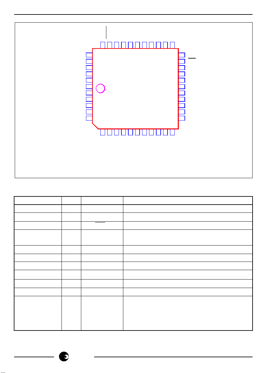
Package : PLCC - 44
PIN DESCRIPTION
Pin No I /0 Designation Description
1, 23 I GND Supply Ground
12, 34 I VCC +5V Power Supply
27 I FS1 Frame Synchronisation (active low)
6 I CLKIN Master clock input (either 8192kHz or 2048 Khz
dependent on logic level of "CLK _SEL")
8 O 2MCLK 2048 kHz clock derived internally from CLKIN
10 O 8KFS 8 kHz Frame Synchronisation output.
5 O PCMFSC 8 kHz Auxilliary Frame Synchronisation Output
11 O INTRFRQ Square Wave Intrude Tone
13 O INTRCAD Intrude Tone Cadence Signal
15 O PCM_OUT Tri-state PCM Highway tone output
41, 42, 43, 44, O A0..A13 EPROM Address Lines
2, 3, 4, 39, 26,
25, 22, 24,
21, 20
2
sames
Page 3
PIN DESCRIPTION (Continued)
DR-01085
T
P
/
D
C
/
C
Pin No I/0 Designation Description
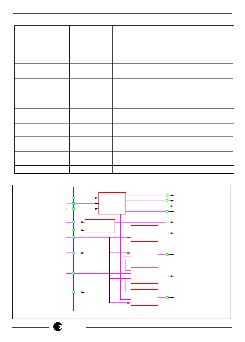
37, 36, 35, 33, I D0..D7 EPROM Data Lines
32, 31, 30, 29
9, 14, 19 I PS0, PS1, Program Select Inputs for Selecting
PS2 between 1 of 8 tone plans
7 O CLKDIV2 CLKIN divided by 2 output (i.e. 4096 kHz or 1024
kHz depending on CLK_SEL input)
40 I CLK_SEL Selects between CKLIN of 8192 or 2048 kHz and
Synchronisation source.
0 = 8192kHz/Internal
1 = 2048kHz/External
28 I TEST Used for IC testing purpose. Tied Low during
normal operation.
38 I MRST Asynchronous Reset Pin. Resets all Internal Flip
Flops (active low)
16 I WD_RST Watchdog reset input (Rising-edge triggered) Tied
high if unused
17 I WD_EN Watchdog enable input (active low) Tied high if
unused
18 O WD_INT Watchdog output (active low, tri-state)
SA9401
BLOCK DIAGRAM
MRST
LK_SEL
LKIN
WD_RST
WDENB
[7 : 0]
FS1
S[2 : 0]
EST
sames
SA9401
CLOCK
GENERATOR
WATCHDOG
TIMER
INTRUDE
TONE
GENERATOR
CADENCE
TIMER
EPROM
INTERFACE
PCM
INTERFACE
CLKDIV2
2MCLK
8KFS
PCMFSC
WD_INT
INTRFRQ
INTRCAD
A[13 : 0]
PCM_OU
3
Page 4

SA9401
FUNCTIONAL DESCRIPTION
The design of the SA9401 has been based on the assumption that any supervisory tone
used in a PABX (e.g. Dial tone or Busy Tone etc) can be described by a small set of
simple parameters and that the tones will be injected into a standard PCM 30 (2048kHz)
backplane in either A-law or µ-law format.
In the SA9401 a tone is created by repeating a fundamental waveform (or one of two
waveforms) which would typically be one cycle of a sinewave or alternatively may be
several cycles of a higher frequency signal (say 400 to 1000Hz) modulated by a lower
frequency signal. This Tone may then be interrupted (“Cadenced”) so that the tone is
effectively switched on and off.
The waveform shape, number of samples per cycle and the cadence can all be set by
the system designer in accordance with the related National Standards.
Once a set of tones have been described they may then be injected into the PCM
backplane. The time slot associated with each tone can be set by the system designer.
The SA9401 accommodates up to 9 different Tones to form a Tone Plan making ample
allowance for Ring, Dial, Busy, Intrude and other Tones. The set of data describing one
Tone Plan (waveforms, cadence timings, timeslots etc) is referred to as a Program and
is stored in an external EPROM which is addressed directly by the SA9401.
Up to eight T one Plans may be stored and selected at will to accommodate products for
multi-national markets.
ARCHITECTURE
The architecture of the SA9401 consists of 6 functional blocks each of which is described in detail in the following sections. Refer also to the block diagram.
Clock Generator
The clock generator circuit derives all the timing for the ic from either a 2048kHz or a
8192kHz clock. The desired Clock is selected by the state of the CLK_SEL pin (1 for
2048kHz and 0 for 8192kHz).
The CLK_SEL pin also determines the function of the Frame Sync pin. If CLK_SEL is
low then Internal synchronisation is assumed and FS1 should be tied high. If CLK_SEL
is high then an external Frame Synchronisation source must be connected to /FS1.
The Clock Generator comprises 5 functional blocks.
A divide-by-4 counter is enabled only if a 8192kHz clock is selected so that all internal
timing is based on 2048kHz. The Time Slot Counter keeps track of the Time Slots (0
to 31) in the PCM Frame while the bit position (0 to 7) in each time-slot is tracked by the
Bit Position Counter. PCM frame synchronisation signals are controlled by the Frame
Generator. Long cadence intervals are accommodated by the Five-ms-Timebase
which delivers a 200Hz signal which clocks the Cadence Timers.
4
sames
Page 5
SA9401
D
Intrude Tone Generator
This module generates a square wave output based on the master clock of 2048kHz.
The Intrude Tone frequency is determined by the contents of the 16-bit Intrude Tone
Register (INTR_LO and INTR_HI) according to the formula:-
f
= 2048kHz/(2*(n+1))
int
where n is the content of the INTR register.
The range of values in the register (from 0 to 65535) give Intrude tones in the range
15.625Hz to 1024kHz.
Cadence Timer
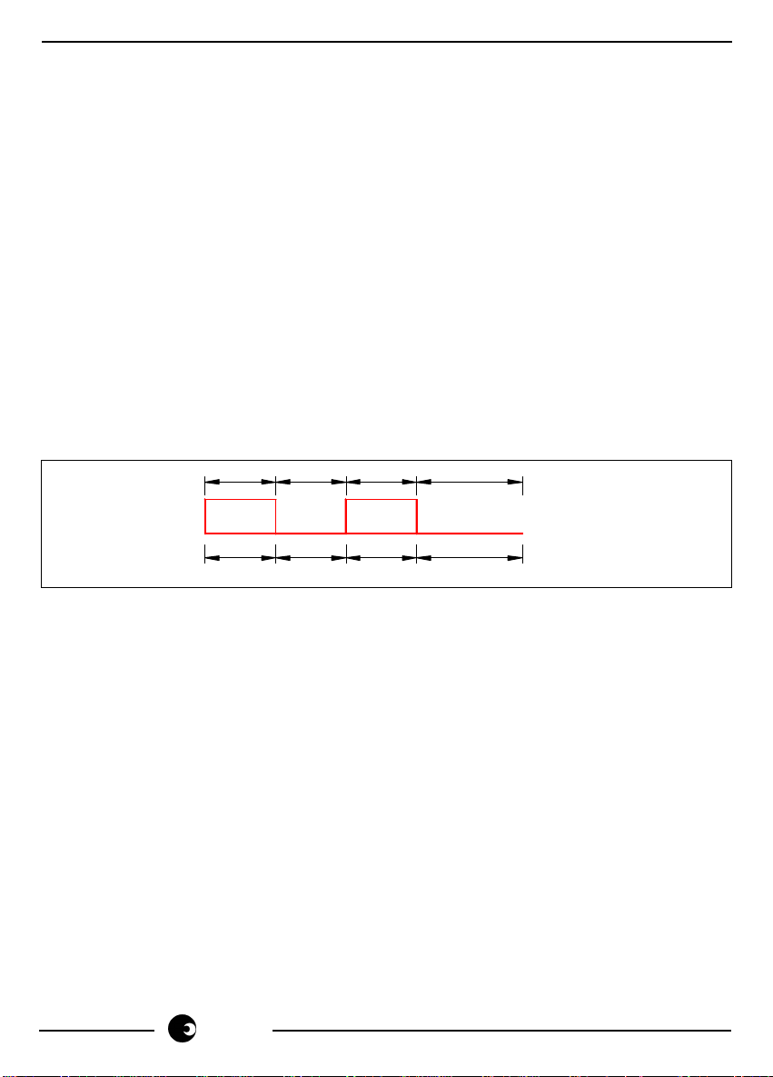
In any given Tone Plan the SA9401 assumes that any or all of the 9 (8 PCM tone
streams and one squarewave Intrude Tone) tones are required to have their own independently defined cadence. A typical cadence is illustrated in FIGURE 1 above. Each
tone is assumed to comprise up to 4 cadence periods which repeat cyclically. The
duration of each period is controlled by the Cadence Timers which in turn comprise 10-
bit Counters. These timers are clocked by the five_ms_timebase generated by the
Clock Generator so that intervals of up to 5.12 seconds can be defined with a resolution
of 5ms. (10 bits => 1023: 1023*5ms = 5115ms)
ON
OFF
OFF
TONE_n_A
CADO_n
R-01086
CAD1_nONCAD2_n
TONE_n_B
CAD3_n
FIGURE 1: TONE CADENCING
The Cadence Controller controls the loading of the 10-bit counter and the sequencing
of the Cadence Position Counter. The duration of each period of the tone is denoted by
the parameter:-
CADm_n_LO = Period m, Tone stream n low-order 8 bits and
CADm_n_HI = Period m, Tone stream n high-order 2 bits
where0 ≤ m ≤ 3 and 0 ≤ n ≤ 8 (8 = Intrude Tone)
The Cadence Position Counter keeps track of the period being generated and during
period 0 the SA9401 generates a tone based on one Tone Block (A) while during the
period 2 (if used) the samples from another Block (B) are used. During periods 1 and 3
the silence sample is transmitted. This feature allows the sound of the tone to be
altered along with the cadence.
A continuous tone is created by loading values of 1(or any non-zero value),0,0,0 into
the registers CAD0_n to CAD3_n respectively. The zero value is interpreted by the
SA9401 as an instruction to ignore the period and to process the next one. With the
register contents shown the Cadence Controller continuously processes the first (ON)
period.
sames
5
Page 6
SA9401
EPROM Interface
The EPROM Interface controls all aspects of the transfer of program and tone data to
the SA9401. This module comprises seven distinct functions.
The Program Select Register reflects the settings on pins PS2 - PS0 which are latched
into the register at the start of every frame. The mapping of the pin settings to the
selected program is by a simple binary code (PS2 = msb).
The Cycle Register is loaded with a 9-bit value (CYCLE) indicating the number of
samples in a Tone Block (or basic waveform). It is assumed that all basic waveforms in
a single Tone Plan will have a common size.
Successive samples in a Tone Block are addressed by the 9-bit Sample Counter which
cycles through from zero to Cycle-1. The current value of this register and the contents
of the Cycle Register are fed to a Comparator which resets the counter after it reaches
the terminal value of Cycle-1.
The required T one Block (or waveform) is addressed by the Tone Block Register. The
content of the register is a function of the Program Select and Cadence Controller.
As previously described, Tone Plans are defined in terms of a basic waveform (Tone
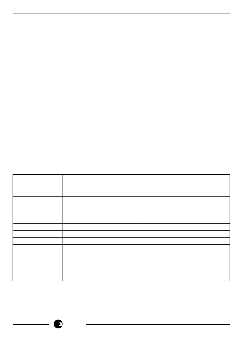
Block) and a Program of descriptive parameters which together are stored in an external EPROM. Consequently a Data Fetch from the EPROM may retrieve either a Program Instruction or a T one Sample. In either case the Address Multiplexer constructs
the address according to the following table.
ADDRESS LINE Program Instruction Fetch Tone Sample Fetch
A13 1 0
A12 0 TONE_BLOCK.3
A11 0 TONE_BLOCK.2
A10 0 TONE_BLOCK.1
A9 PSEL2 TONE_BLOCK.0
A8 PSEL1 SAMPLE_COUNT.8
A7 PSEL0 SAMPLE_COUNT.7
A6 PC6 SAMPLE_COUNT.6
A5 PC5 SAMPLE_COUNT.5
A4 PC4 SAMPLE_COUNT.4
A3 PC3 SAMPLE_COUNT.3
A2 PC2 SAMPLE_COUNT.2
A1 PC1 SAMPLE_COUNT.1
A0 PC0 SAMPLE_COUNT.0
The details of the Address mapping will be described later in the External Data Stor-
age section
6
sames
Page 7

SA9401
PCM Interface
The PCM Interface controls all aspects of the transfer of PCM signals onto the PCM
highway.
Eight-bit Tone Registers store the PCM tone samples and are updated once per PCM
frame. Before a PCM word is transmitted to the PCM highway the Tone Selector
determines whether or not the Cadence controller requires an OFF period. If so then a
specific PCM word for Silence (held in the Silence Register) is substituted for the tone
sample.
The actual transfer of the tone (or silence) samples to the PCM highway is the function
of the Injection Controller. Time Slot Registers indicate to which PCM time-slot the
sample is to be injected. These registers (one for each tone stream) comprise 5 address bits and one (high-order) enabling bit. A Comparator checks if the Time Slot
Register contents match the current PCM time-slot and if so feeds the T one Sample (or
Silence Sample) into the Parallel In Serial Out module and the required sample is
clocked out via the PCM_OUT pin. The PCM_OUT pin is enabled only when samples
are being clocked out (ie when the 5 least significant bits of the Time Slot Register
matches the current PCM Time Slot and the Time Slot Register MSB is Low) and is
held in a tri-state condition at all other times.
Watchdog Timer
The watchdog timer performs a function completely independently of the Universal Tone
Generator. Its operation is described below.
The watchdog timer comprises three I/O pins, viz;
WD_EN - an active low input which enables/disables the watchdog.
WD_RST - a rising edge triggered input which resets the watchdog timer and
prevents the output from resetting the microprocessor.
WD_INT - an active low tri-state output which when active, resets a micro-
processor.
The watchdog timer operates as follows:
- For the watchdog timer to operate, the WD_EN pin must be held low (i.e. active).
With the WD_EN pin held high, the WD_INT output remains tri-stated.
The delay between WD_EN going active and a WD_INT output is 2 seconds.
- The timer is reset every time a rising edge is detected on the WD_RST pin. The
minimum pulse width of the WD_RST input is two CLKIN periods.
- The WD_INT output comprises an active low pulse of 5 milliseconds followed by a
tri-state period of 1995 milliseconds (assuming no valid WD_RST pulse is detected
within 2 seconds of the previous WD_RST pulse).
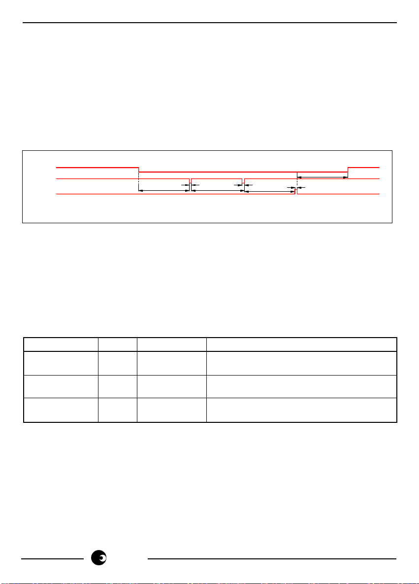
The timing diagram for the Watchdog Timer is given in Figure 2. Note that although the
timebase for the Watchdog Timer is always 2048kHz, the WD-EN and WD-RST inputs
are strobed at the external clock rate.
sames
7
Page 8
SA9401
FIGURE 2
EXTERNAL DATA STORAGE
This section describes in detail the names and definition of the parameters which define the T one Plan for a PABX. Values for these parameters are selected by the system
designer in accordance with the relevant standards and are saved in an external EPROM
to be addressed by the SA9401.
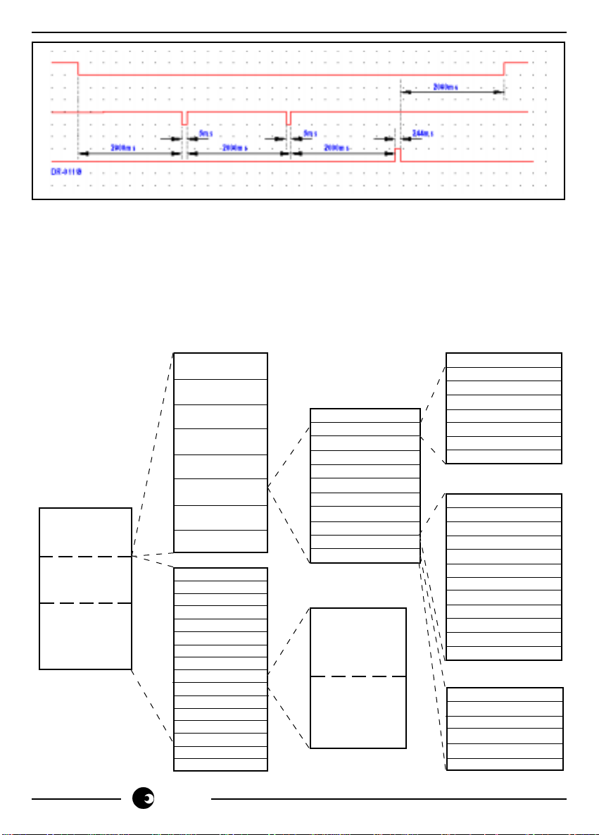
Reference can be made to the diagram of fig. 3 which defines the memory map of the
EPROM.
3FFFH
Unused
2400H
23FFH
Programs
2000H
1FFFH
Tone
Blocks
0000H
16kbyte
EPROM
23FFH
2380H
237FH
2300H
22FFH
2280H
227FH
2200H
21FFH
2180H
217FH
2100H
20FFH
2030H
207FH
2000H
1E00-1FFFH Tone Blk F
1C00-1DFFH E
1A00-1BFFH D
1800-19FFH C
1600-17FFH B
1400-15FFH A
1200-13FFH 9
1000-11FFH 8
0E00-0FFFH 7
0C00-0DFFH 6
0A00-0BFFH 5
0800-09FFH 4
0600-07FFH 3
0400-05FFH 2
0200-03FFH 1
0000-01FFH 0
Program 7
Program 6
Program 5
Program 4
Program 3
Program 2
Program 1
Program 0
+ 6E-7FH Not Used
+66-7DH Intrude Tone
+5A-65H Tone Stream 7
+ 4E-59H 6
+ 42-4DH 5
+ 36-41H 4
+ 2A-35H 3
Program p
+ 1E-29H 2
+ 12-1DH 1
+ 06-11H 0
+00-05H Initialisation
BASE ADDR = 2000 + p * 80H
BASE + 1 FFH
Unused
BASE + CYCLE
BASE + CYCLE - 1
T one Block b
PCM Samples
BASE ADDR (b * 0200H)
+ 6DH CAD3_8_HI
+ 6CH CAD3_8_LO
+ 6BH CAD2_8_HI
+ 6AH CAD2_8_LO
+ 69H CAD1_8_HI
+ 68H CAD1_8_LO
+ 67H CAD1_8_HI
+ 66H CAD0_8_LO
BASE ADDR = 2000 + p*80H
+ 11H TIME_SLOT_n
+ 10H CAD3_n_HI
+ 0FH CAD3_n_LO
+ OEH CAD2_n_HI
+ ODH CAD2_n_LO
+ OCH CAD1_n_HI
T one stream n
+ OBH CAD1_n_LO
+ 0AH CAD0_n_HI
+ 09H CAD0_n-LO
+ 08H Unused
+ 07H TONE_BLOCK_n-B
+ 06H TONE_BLOCK_n_A
BASE = 2000+ P*80+ n*CH
+ 05H INTR_HI
+ 04H INTR_LO
+ 03H SILENCE
+ 02H CYCLE_HI
+ 01H CYCLE_LO
+ 00H Unused
8
sames
Page 9
SA9401
5ms
2000ms
WD_EN
WD_INT
WD_RST
244ms
2000ms
5ms
2000ms
2000ms
DR-01119
The EPROM contents can be divided into two distinct sections. The smaller section
contains eight Programs, each of which would typically describe all the tones required
by a PABX used in a single country. Thus a single EPROM can be programmed to
cover up to eight different countries requirements.
The larger part of the EPROM is occupied by the sets of PCM samples which make up
the basic waveforms to be used by the SA9401 in creating the familiar supervisory
tones. Each of 16 waveforms can contain up to 511 samples of A or µ law samples.
Program
A single Program comprises one set of Initialisation Data, 8 PCM Tone Streams with
the associated Cadence, Timeslot and Waveform and one Intrude Tone with its asso-
ciated Cadence. Each individual variable is described below.
Initialisation
The Initialisation data describes parameters common to all the tones in a given plan.
Variable bits Composition Description
CYCLE 9 CYCLE_HI Identifies the number of samples in the
CYCLE_LO Tone Block. (from 1 to 511 )
SILENCE 8 The Silence sample to be used during
cadence period 1 and 3.
INTR 16 INTR_HI The divisor used to generate the
INTR_LO Intrude Tone Frequency.
PCM Tone Stream
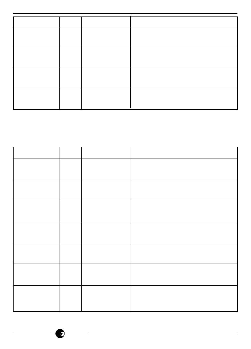
The Tone Stream Data describes the characteristics of a specific PCM Tone. Note that
the length of the Cadence periods are defined in multiples of 5ms.
sames
9
Page 10
SA9401
Variable Bits Composition Description
CAD0_8 10 CAD0_8_HI Length of the first (ON) cadence
CAD0_8_LO period.
CAD1_8 10 CAD1_8_HI Length of the second (OFF) cadence
CAD1_8_LO period.
CAD2_8 10 CAD2_8_HI Length of the third (ON) cadence
CAD2_8_LO period.
CAD3_8 10 CAD3_8_HI Length of the Fourth (OFF) cadence
CAD3_8_LO period.
Intrude Tone
This data describes the characteristics of the Intrude Tone Cadence output on pin
INTRCAD of the SA9401.
Variable Bits Composition Description
TONE_BLOCK 4 Number of the Tone Block to be used
_n_A in the first Cadence period.
TONE_BLOCK Number of the Tone Block to be used in
_n_B 4 the third Cadence period.
CAD0_n 10 CAD0_n_HI Length of the first (ON) cadence period.
CAD0_n_LO
CAD1_n 10 CAD1_n_HI Length of the second (OFF) cadence
CAD1_n_LO period.
CAD2_n 10 CAD2_n_HI Length of the third (ON) cadence period.
CAD2_n_LO
CAD3_n 10 CAD3_n_HI Length of the Fourth (OFF) cadence
CAD3_n_LO period.
TIME_SLOT_ 6 The number of the Time Slot into which
n the tone is to be injected.
Valid only if MSB is Low.
10
sames
Page 11
SA9401
DR-01087
1 / 33.3Hz = 30ms
30ms @ 8k SAMPLES / sec = 240 SAMPLES = CYCLE
1 / 400Hz = 2.5ms
NOTE THAT SIGNAL
AND ENVELOPE
START ON ZERO
CROSSING POINT
Tone Waveform
The frequency content of any desired tone is defined by taking one cycle of the tone
(which may be a simple or complex waveform) and calculating the series of PCM sam-
ples which would result if that tone were passed through a CODEC. The definition of a
waveform is perhaps best illustrated by way of an example.
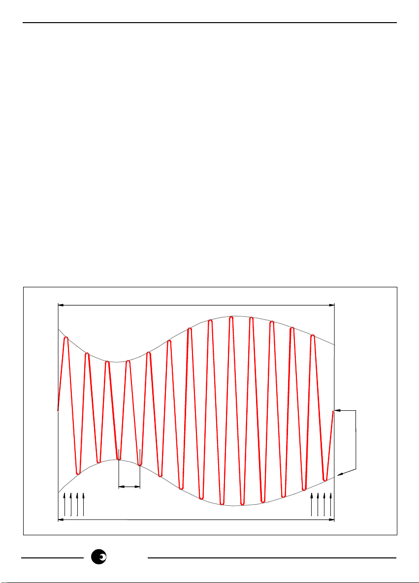
Consider the case of a PTT dial tone which is a signal of 400Hz modulated at 33.33Hz
as illustrated in fig. 4 below. The first step is to identify the lowest frequency in the
composite signal, in this case 33.33Hz. Next the designer should confirm that one
cycle of the lower frequency component of the signal will contain an integer number of
cycles of the higher frequency component. In the example there are exactly 12 cycles
of the 400Hz signal contained within the one cycle of the modulating signal. If this is
not the case then the tone sample should be designed to contain two or more cycles of
the lower frequency tone, subject to the maximum of 512 samples. It is also typical to
take a block of the signal which starts and ends at two similar zero crossing points.
Although any arbitrary point in the waveform may be used a careless choice may lead
to the introduction of undesirable harmonics.
Having chosen a suitable tone sample it is possible to determine the value for CYCLE
as the size of the tone block is simply the number of samples (at 8k samples per
second) which fall into the waveform chosen. In the example CYCLE = 240 samples =
F0H.
FIGURE 4 400Hz Tone modulated at 33.33Hz.
sames
11
Page 12
SA9401
Finally the system designer should calculate the PCM sample value for each of the 240
samples in the block. The PCM values used may of course be calculated according to
either A or µ-law and adjusted to suit the required amplitude.
Up to 16 Tone Blocks may be defined each with a maximum of 511 samples. Tone
Blocks are stored in the EPROM starting at address b * 0200H where b is the number of
the block from 0 to 15 (decimal).
APPLICATION INFORMATION
To simplify the translation of Tone Plan requirements to EPROM data SAMES offer a
Support Software pack. This elegant package will guide the designer through the definition of T one Plans and translate the requirements into a hex source file ready for most
commonly used PROM programmers. For more details contact your nearest SAMES
representative.
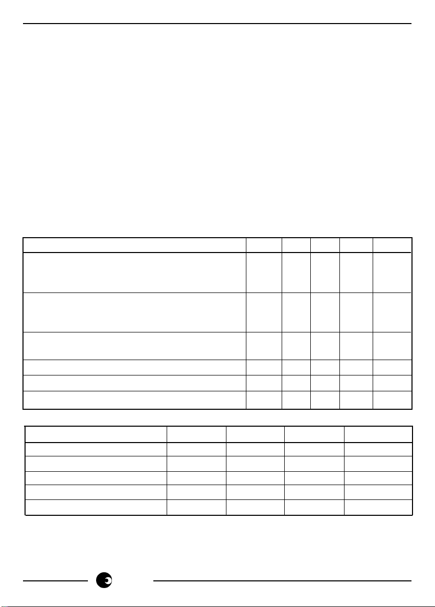
AC PARAMETERS
TA = 0°C to + 70°C, VCC = 5V ± 5%. Load Cap<= 50pf
AC PARAMETERS SYM MIN TYP MAX UNITS
Propagation delay of outputs synchronous to Pd
CLKIN (i.e. 2MCLK, CLKDIV2, and
WD_INT) relative to CLKIN rising clock edge
Propagation delay of outputs synchronous Pd
to 2MCLK (i.e. INTRFRQ, 8KFS, PCMFSC,
INTRCAD, PCM_OUT, A0..A13
Delay to float of PCM_OUT AFTER LAST BIT Pf
OF TIME-SLOT OUTPUT
Delay to float of WD_INT after going inactive Pf
D0..D7 setup to 2MCLK rising edge SdD100 ns
D0..D7 hold after 2MCLK rising edge Hd
02040 ns
8M
02040 ns
2M
03060 ns
po
03060 ns
WD
0ns
D
Absolute Maximum Ratings*
Parameters Symbol Min Max Unit
Supply Voltage V
Voltage on any I/O pin V
Current on any I/O pin I
Storage Temperature T
Package Power Dissipation P
DD
I/V0
I/I0
SIG
D
-0.3 7.0 V
-0.3 VDD +0.3 V
-10 +10 mA
-55 +125 °C
1000 mW
* Stress above those listed under "Absolute Maximum Ratings" may cause permanent damage
to the device. This a stress rating only. Functional operation of the device at these or any other
condition above those inidcated in the operational sections of this specification, is not implied.
Exposure to Absolute Maximum Ratings for extended periods may effect device reliability.
12
sames
Page 13
SA9401
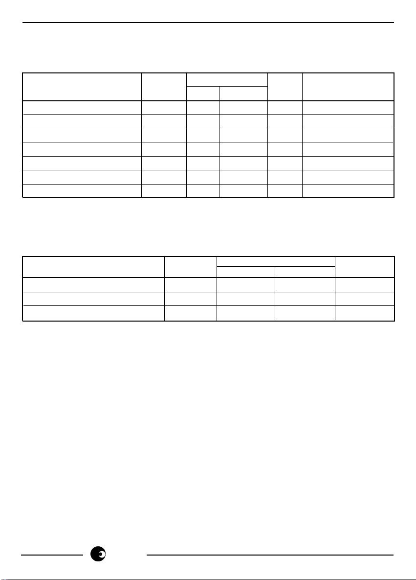
DC Characteristics
T
= 0 to 70°C; VDD = 5V ± 5%; VSS = OV
A
Limit Values
Parameter Symbol Min. Max. Unit Test Conditions
L-input voltage V
H-input voltage V
L-input voltage V
H-output voltage V
OL
OH
IL
IH
4.0 VDD+0.3 V VDD = 5V
4.5 V IOH = 0.1mA
Operating Frequency 2.273 MHz V
Input leakage current I
Output leakage current I
LI
LO
-10 10 µA 0V < V
-10 10 µA 0V < V
Characteristics
T
= 25°C; VDD = 5V ±5%; V
A
SS
= OV
Parameter Symbol Min. Max. Unit
Input capacitance C
Output capacitance C
I/O C
IN
OUT
IO
1.0 V VDD = 5V
0.5 V IOL = 0.1mA
= 5V
DD
< V
IN
OUT
Limit Values
10 pF
15 pF
20 pF
DD
< V
DD
sames
13
Page 14
SA9401
0
7
6
5
4
TIME-SLOT 0
3
2
1
0
7
6
5
4
TIME-SLOT 31
3
2
1
0
7
0
7
6
5
4
TIME-SLOT 0
3
2
1
0
7
6
5
4
TIME-SLOT 31
3
2
1
0
0
7
PCM OUTPUT STRUCTURE
6
5
4
3
2
1
0
7
6
5
4
3
2
1
0
6
7
0
1
2
3
4
TIME-SLOT 0
TIME-SLOT 31
PCM FRAME SYNCHRONIZATION SIGNALS
5
6
7
CLKIN
CLKDIV2
2MCLK
8kFS
PCM_OUT
PCMFSC
CLKIN
CLKDIV2
2MCLK
8kFS
PCM_OUT
PCMFSC
DR-00750
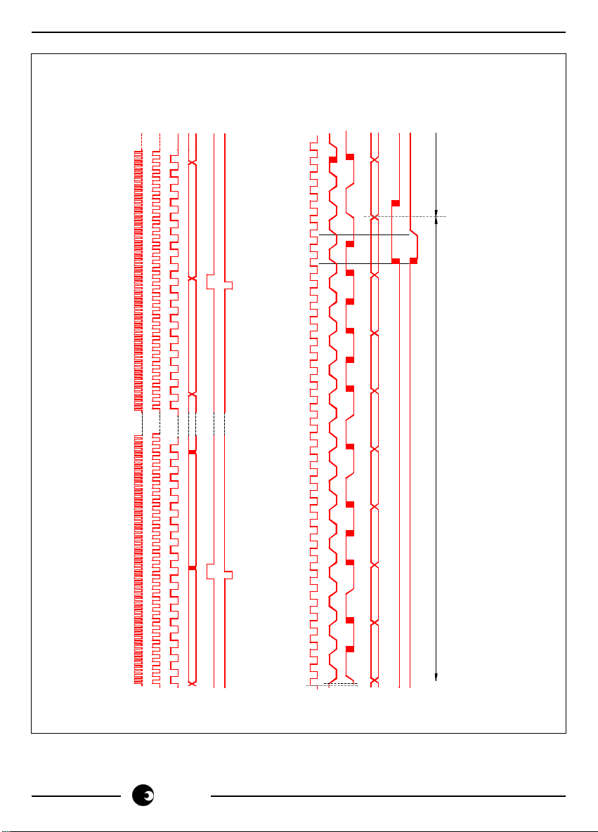
Figure 5 - Timing Diagram (CLK_SEL=0, CLKIN=8MHz, Internal Sync.)
14
sames
Page 15
SA9401
0
7
6
5
4
3
2
1
0
7
6
5
4
TIME-SLOT 31
3
2
1
0
7
0
7
6
5
4
TIME-SLOT 0
3
2
1
0
7
6
5
4
3
2
1
0
TIME-SLOT 0
TIME-SLOT 31
0
7
PCM OUTPUT STRUCTURE
6
5
4
3
2
1
0
7
6
5
4
3
2
1
0
6
7
0
1
2
3
4
TIME-SLOT 0
TIME-SLOT 31
PCM FRAME SYNCHRONIZATION SIGNALS
5
6
7
CLKIN
CLKDIV2
2MCLK
8kFS
PCM_OUT
PCMFSC
CLKIN
CLKDIV2
2MCLK
PCM_OUT
8kFS
PCMFSC
DR-00750
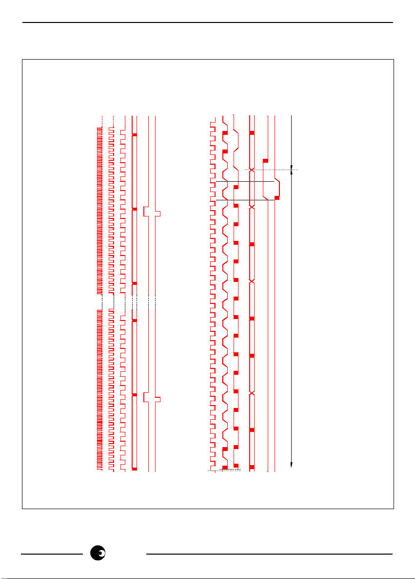
Figure 6 - TIMING DIAGRAMS (CLK_SEL = 1, CLKIN = 2MHz, EXTERNAL SYNC.)
sames
15
Page 16

SA9401
Disclaimer: The information contained in this document is confidential and proprietary to South African Micro-
Electronic Systems (Pty) Ltd ("SAMES") and may not be copied or disclosed to a third party, in whole or in part,
without the express written consent of SAMES. The information contained herein is current as of the date of
publication; however, delivery of this document shall not under any circumstances create any implication that the
information contained herein is correct as of any time subsequent to such date. SAMES does not undertake to
inform any recipient of this document of any changes in the information contained herein, and SAMES expressly
reserves the right to make changes in such information, without notification,even if such changes would render
information contained herein inaccurate or incomplete. SAMES makes no representation or warranty that any
circuit designed by reference to the information contained herein, will function without errors and as intended by
the designer.
Any sales or technical questions may be posted to our e-mail adress below:
[email protected]
For the latest updates on datasheets, please visit our web site:
http://www.sames.co.za
South African Micro-Electronic Systems (Pty) Ltd
P O Box 15888, 33 Eland Street,
Lynn East, Koedoespoort Industrial Area,
0039 Pretoria,
Republic of South Africa, Republic of South Africa
Tel: 012 333-6021 Tel: Int +27 12 333-6021
Fax: 012 333-8071 Fax: Int +27 12 333-8071
16
sames
 Loading...