

Page 1

INTEGRATED CIRCUITS
SA900
I/Q transmit modulator
Preliminary specification 1997 Sept 16
IC17 Data Handbook
Page 2
Philips Semiconductors Preliminary specification
SA900I/Q transmit modulator
DO NOT DISTRIBUTE WITHOUT ECN DATED AFTER Sept 16, 1997
DESCRIPTION
The SA900 is a monolithic high performance, multi-function transmit
modulator for use in cellular radio applications, fabricated in QUBiC
BiCMOS technology. The SA900 features both analog (AMPS)
mode and complex, I/Q digital (NADC IS–136) mode quadrature
modulation functions, a PLL synthesizer with VCO, crystal oscillator,
programmable prescalers and Gilbert cell multiplier phase detector
with programmable charge pump output. The DUALTX output can
be used in DUAL mode cellular phone applications with the AMPS
and NADC modulation being applied to the I/Q baseband inputs.
The DUALTX output also provides 6-bit power control with 40dB of
gain control in 0.63dB steps. In addition, buffered crystal oscillator
programmable prescaler outputs are provided to support system
clock reference needs. Programming of the SA900 functions are
realized by a high speed 3-wire serial interface. The SA900 can be
programmed into a sleep mode (low current mode providing crystal
oscillator and Master Clock functions), a standby mode (providing
crystal oscillator, Master Clock, System Clock 1 and Transmit LO
buffer functions), and the AMPS mode and the DUAL mode
configurations.
FEA TURES
•V
= 4.0V
CC
•Tx output frequency = 900MHz
•Direct modulation of RF
•DUAL mode, on-chip PA control
•I/Q modulator
•Single sideband quadrature LO generation with no external
adjustments required
•On-chip crystal oscillator with 3 buffered outputs
•AMPS/TACS compatible
•On-chip VCO
PIN CONFIGURATION
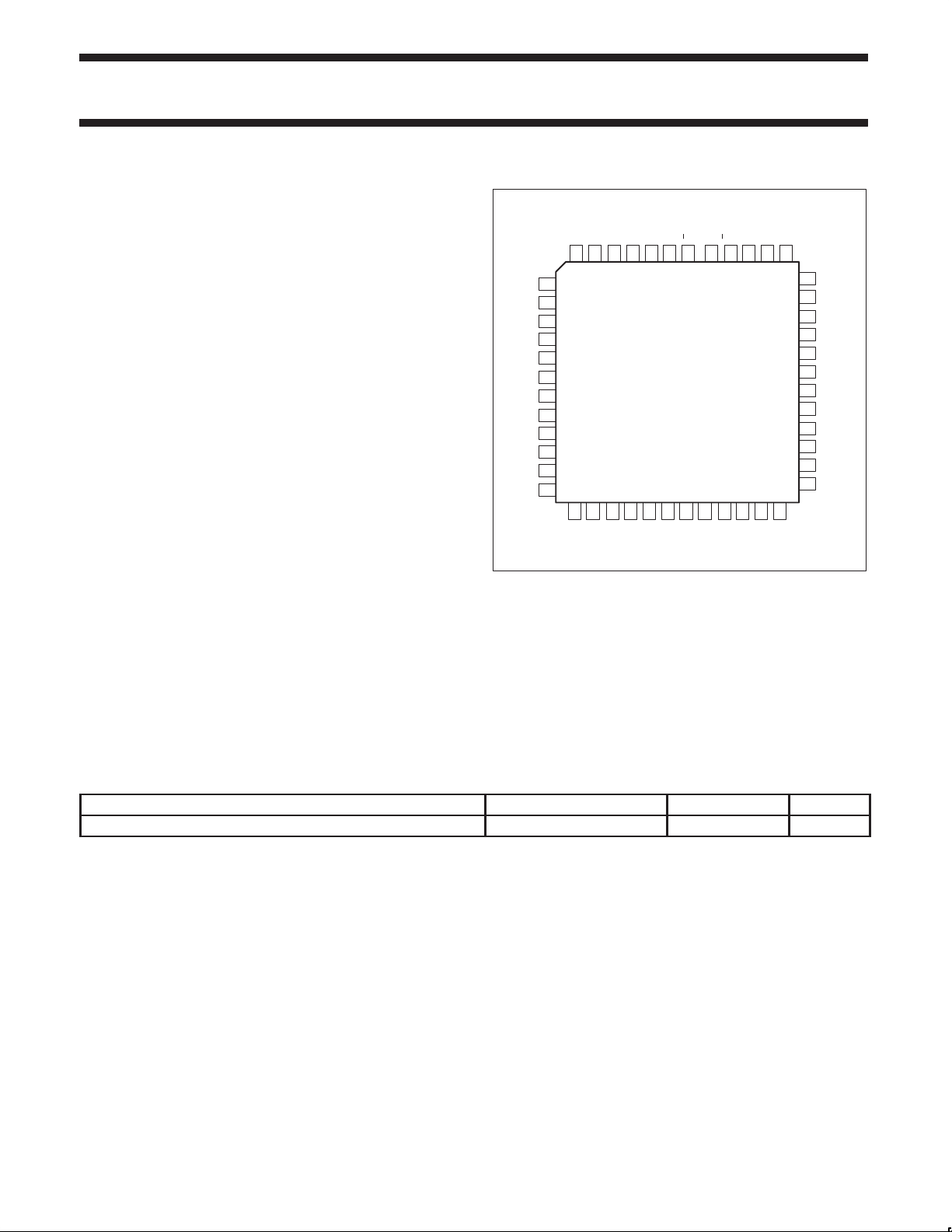
BE Package
I
Vcc
CLK2
GND
I
QQGND
424344
20 21 22 23 24
DATA
MCLK
CLKSET
394041 3738
CLOCK
GND
TXLO_2
TXLO_1
GND
Vcc
TANK_1
TANK_2
Vcc
PHSOUT
I
PEAK
GND
XTAL_1
Vcc
LO_2
LO_1
1
2
3
4
5
6
7
8
9
10
11
12
13 14 15 16 17 18 19
Vcc
CLK1
XTAL_2
GND
45464748
GND
Figure 1. Pin Configuration
•Selective power-down
– Low power AMPS/TACS mode
– Low power dual mode NADC
•48-Pin TQFP package
APPLICATIONS
•North American Digital Cellular (TDMA IS-136)
Vcc
GND
TXEN
STROBE
36
35
34
33
32
31
30
29
28
27
26
25
Vcc
GND
DUALTX
GND
Vcc
AMPSTX
GND
Vcc
GND
Vcc
Vcc
GND
SR00636
ORDERING INFORMATION
DESCRIPTION TEMPERATURE RANGE ORDER CODE DWG #
48-Pin Plastic Low Profile Quad Flat Package (LQFP)
1997 Sept 16 853-
2
-40 to +85°C
SA900BE SOT313-2
Page 3
Philips Semiconductors Preliminary specification
SA900I/Q transmit modulator
BLOCK DIAGRAM
TXLO_2
TXLO_1
TANK_1
TANK_2
PHSOUT
I
PEAK
XTAL_1
XTAL_2
LO_2 LO_1
VCO
÷N
÷A8/1
PHS
DET
XTAL
OSC
AD
÷B8/1
TXLO
LPF
IMAGE
REJECT
VCO
MIXER
2
AD
AD
÷÷÷
SM1 SM2
SM1 SM2
XY
3/1 4/5/1
2/1
PHASE
SHIFT
NETWORK
BIAS
LPF
LPF
BG
CONV2
II QQ
SE
N<0:1>
AD
SM1
SM2
Y
X
VGA PA
VGA
CONTROL
CONTROL
LOGIC
DUALTX
PA
6
AMPSTX
CLK2CLK1
MCLK
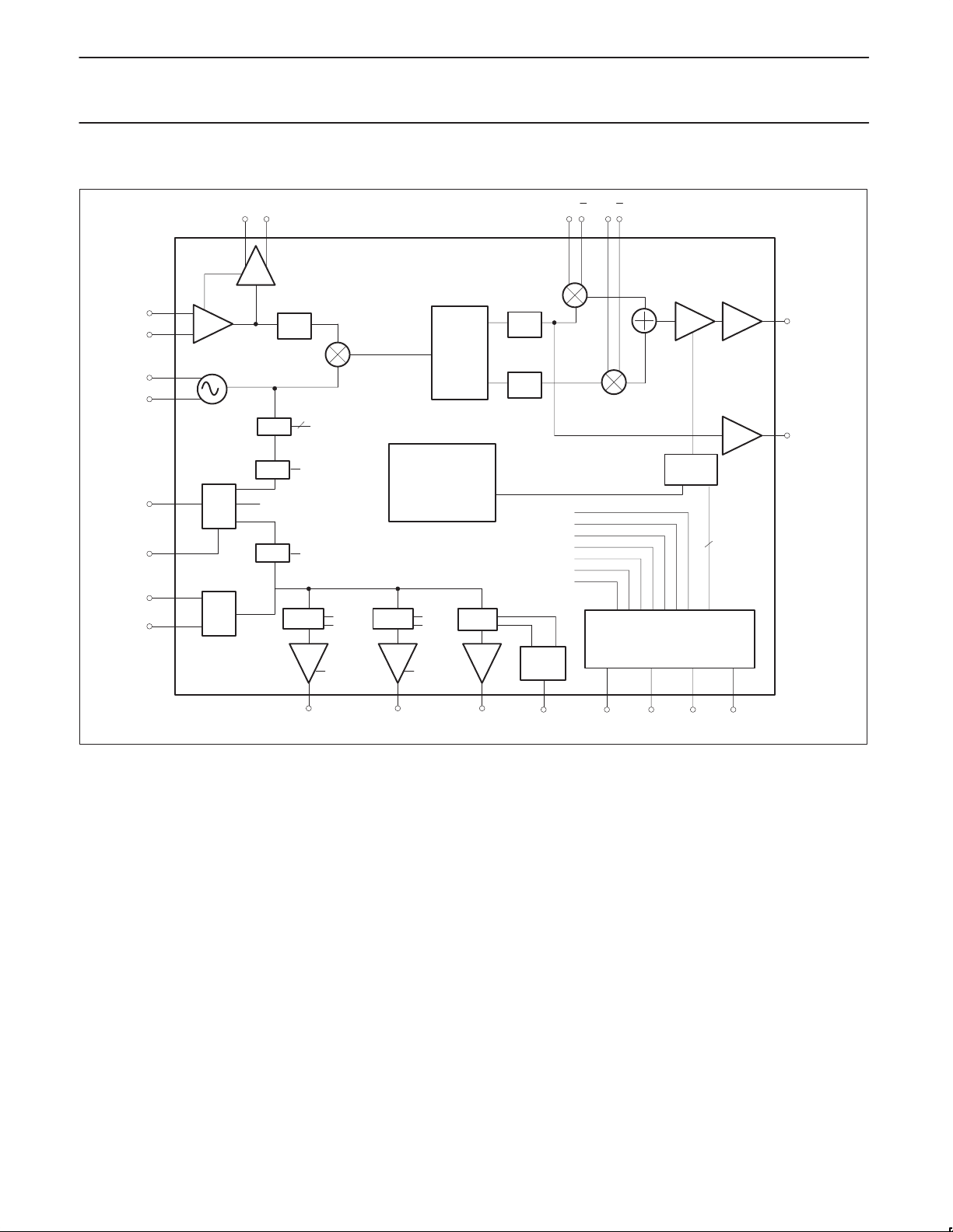
Figure 2. Block Diagram
TXENSTROBECLOCKDATACLKSET
SR00637
1997 Sept 16
3
Page 4

Philips Semiconductors Preliminary specification
SA900I/Q transmit modulator
PIN DESCRIPTIONS
Pin Description
I Non-inverting I Mod Signal
I Inverting I Mod Signal
TXLO_1/2 Second LO Input (differential/single-ended input)
DUALTX RF output (850MHz) digital (DUAL) mode, complex modulated output
Q Non-inverting Q Mod Signal
Q Inverting Q Mod Signal
CLK1 Buffered oscillator output (XO ÷3/÷1)
MCLK Buffered oscillator output (XO ÷4/÷5/÷1)
CLK2 Buffered oscillator output (XO ÷2/÷1)
AMPSTX RF output (850MHz) AMPS mode
V
CC
GND Ground
Data Serial data input
Clock Serial clock input
Strobe Data strobe input
TXEN AMPS and Dual Mode transmit enable
CLKSET Program control pin for MCLK prescaler
XTAL1 Crystal oscillator base input
XTAL2 Crystal oscillator emitter output
PHSOUT Phase comparator charge pump output
TANK_1 VCO differential tank
TANK_2 VCO differential tank
LO_1/2 Buf fered dif ferential TXLO output
I
PEAK
+5VDC power supply
Phase comparator current programming
1997 Sept 16
4
Page 5
Philips Semiconductors Preliminary specification
SA900I/Q transmit modulator
GND_LO GND GND GND GND GND_CTRL GND GND GND GND GND GND GND
1 4 11 16 18 25 28 30 33 35 37 39 45
GND
VCC_LO VCC_CTRLVCCVCCVCCV
48 5 8 14 27 29 32 36 38 44 26
V
CC
2
V
CC
3
V
CC
6
CC
50Ω
50Ω
V
CC
VCCVCCVCCV
CC
9
1997 Sept 16
V
CC
7
V
CC
V
CC
0.1/6.4 mA
0.1/6.4 mA
12
V
CC
13
SR00638
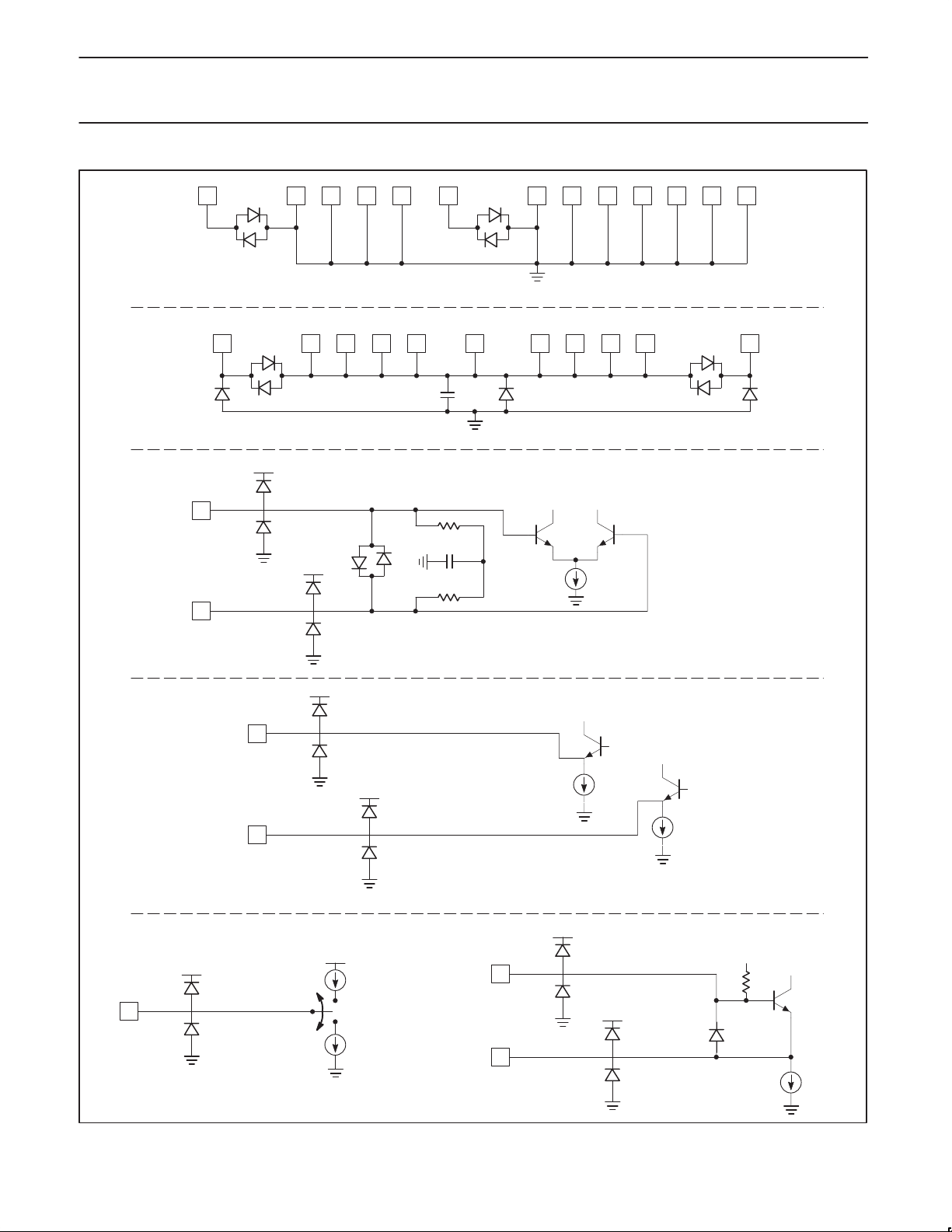
Figure 3. Pin Diagrams
5
Page 6
Philips Semiconductors Preliminary specification
SA900I/Q transmit modulator
V
CC
19
1715
V
CC
23
2221
V
CC
31
30Ω
24
V
CC
500Ω
20
34
V
CC
500Ω
V
CC
600Ω
42
40
680Ω680Ω
V
CC
43
41
V
CC
47
46
20Ω
SR00639
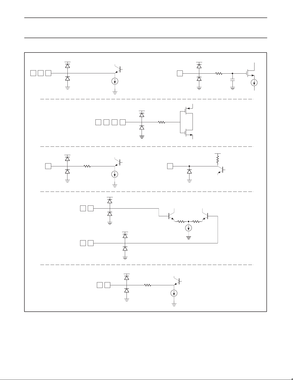
Figure 4. Pin Diagrams (cont.)
1997 Sept 16
6
Page 7

Philips Semiconductors Preliminary specification
SYMBOL
PARAMETER
TEST CONDITIONS
UNITS
ICCSupply current
mA
SA900I/Q transmit modulator
ABSOLUTE MAXIMUM RATINGS
SYMBOL PARAMETER RATING UNITS
V
CC
V
IN
P
D
T
JMAX
P
MAX
T
STG
NOTE:
1. Maximum dissipation is determined by the operating ambient temperature and the thermal resistance, θ
RECOMMENDED OPERATING CONDITIONS
SYMBOL PARAMETER RATING UNITS
V
CC
T
A
T
J
Supply voltage -0.3 to +6 V
Voltage applied to any other pin -0.3 to (VCC + 0.3) V
Power dissipation, TA = 25°C (still air) 600 mW
Maximum operating junction temperature 150 °C
Maximum power input/output +10 dBm
Storage temperature range –65 to +150 °C
.
48-pin LQFP: θ
= 67°C/W
JA
JA
Supply voltage 3.9 to 5.1 V
Operating ambient temperature range -40 to +85 °C
Operating junction temperature -40 to +105 °C
DC ELECTRICAL CHARACTERISTICS
VCC = +4.0V , TA = 25°C; unless otherwise stated.
MIN TYP MAX
V
Power supply range 3.9 5.1 V
CC
Sleep mode 3.1
pp
Standby mode 8.2
AMPS mode 27.5
DUAL mode 64
I / I In-phase differential baseband input DC 0.5V
Q / Q Quadraphase differential baseband input DC 0.5V
÷ 4
CLKSET Divide by 4/5/1
÷ 5
÷ 1
V
V
Clock, data, strobe, TXEN Input low –0.3 0.3V
IL
Clock, data, strobe, TXEN Input high 0.7V
IH
CC
LIMITS
CC
CC
V
CC
0.5V
CC
0
CC
VCC+0.3 V
V
V
V
V
1997 Sept 16
7
Page 8

Philips Semiconductors Preliminary specification
SYMBOL
PARAMETER
TEST CONDITIONS
UNITS
dBm
I
PHSOUT programming
XTAL_1
XO transistor base
CLK2
DUALTX
SA900I/Q transmit modulator
AC ELECTRICAL CHARACTERISTICS
VCC = +4.0V, TA = 25°C; TANK_1 = 120MHz @ 0 dBm; XO_REF = 30MHz @ –5 dBm; TxLO2 = –13 dBm, unless otherwise stated.
LIMITS
MIN TYP MAX
45
1
1
1
1
1
CC
1
1
MHz
MHz
1
mV
P-P
MHz
P-P
MHz
P-P
MHz
P-P
MHz
1
V
V
2
MHz
Input power -13 -10
TXLO_1/2 Transmit LO input (AC couple) (50Ω) VSWR (50Ω) 2:1
Frequency range 900 1040 MHz
TANK_1/2 VCO tank differential inputs Frequency range 90
1
120 140
PHSOUT Phase detector charge pump output Output level 0.5 VCC–0.5 V
R
= 24kΩ, AD=0 200 300 400 µA
PEAK
CLK1
p
XO divide 3/1, power down SM1=0, 50%
duty cycle
SET
R
= 24kΩ, AD=1 0.9 1.2 1.5 mA
SET
XO frequency 10
External drive 150
Frequency range 3.33
1
1
1
30 45
350 500
30 45
÷3, X=1, ÷1, X=0 Output level, 5kΩ || 7pF 0.7 1 1.4 V
XO divide 2/1, power down SM2=0 Frequency range 5
1
30 45
÷2, Y=1, ÷1, Y=0 Output level, 5kΩ || 7pF 0.7 1 1.4 V
1
MCLK
XO divide 4/5/1, 50% duty cycle Frequency range 2
÷4, CLKSET = VCC, ÷5, CLKSET = 0.5VCC,
÷1, CLKSET = 0V
Output level, 5kΩ || 7pF 0.7 1 1.4 V
Serial data clock input, 33% duty cycle Max clock rate 10
CLOCK Serial interface (CMOS levels) Logic LOW 0.3V
DATA, CLOCK, STROBE, TXEN Logic HIGH 0.7V
AMPS output, SE=1, AD=0, TXEN=1 (AC
couple)
Frequency range 820 860 MHz
CC
VSWR 2:1
Output level –1.5 +2 dBm
869 to 894MHz -104 dBm
824 to 849MHz -47 dBc
AMPSTX
Spurious output 2 to 824MHz -41 dBc
849 to 869MHz -41 dBc
894MHz to 8.49GHz -41 dBc
TXLO and harmonics -21 dBc
Adjacent channel noise power @30kHz -95 dBc/Hz
Alternate channel noise power @60kHz -101 dBc/Hz
Broadband noise power 869 to 894MHz -136 dBm/Hz
DUAL output, SE=1, AD=1, TXEN=1 (with
external matching Figure 9)
Frequency range 820 920
VSWR 2:1
Output level (avg) (I and Q
quad, 0dB VGA)
0 +2 dBm
Gain flatness 1 dB
1997 Sept 16
8
Page 9

Philips Semiconductors Preliminary specification
SYMBOL
PARAMETER
TEST CONDITIONS
UNITS
Broadband noise (0dB VGA)
_
Output impedance
Out ut level
SA900I/Q transmit modulator
AC ELECTRICAL CHARACTERISTICS (continued)
LIMITS
MIN TYP MAX
DUALTX 3rd order -35 -42 dBc
(cont.) Linearity (0dB VGA, I and Q inphase) 5th order -55 dBc
7th order -65 dBc
Carrier suppression (I and Q quadrature) VGA = 0dB -35 -45 dBc
Carrier suppression (I and Q quadrature) VGA = –40dB -28 -33 dBc
Sideband suppression I and Q quadrature -35 -45 dBc
869 to 894MHz –104 dBm
824 to 849MHz –47 dBc
Spurious output 2 to 824MHz –41 dBc
849 to 869MHz –41 dBc
894MHz to 8.49GHz –41 dBc
TXLO and harmonics –21 dBc
869 to 894MHz –136 dBm/Hz
935 to 960MHz –136 dBm/Hz
Adjacent channel noise power @30kHz –95 dBc/Hz
Alternate channel noise power @60kHz –101 dBc/Hz
Max frequency 0.8 2
Q/Q Baseband quadrature differential input Differential modulation level 0.6
Differential input impedance 10
1
1
Max frequency 0.8 2
I/I Baseband inphase differential input Differential modulation level 0.6
1
Differential input impedance 10 kΩ
Buffered TXLO differential outputs (AC
coupled)
Frequency range 900 1040 MHz
VSWR (single-ended) 2:1
LO_1/2
p
p
p
single-ended 50 Ω
differential 100 Ω
single-ended, 50Ω 50 90 mV
differential, 100Ω 100 180 mV
NOTES:
1. Guaranteed by design.
2. Needs a different matching component. Max test frequency is 850MHz with test circuit shown in Figure 11.
0.8 1.0
0.8 1.0
1
1
MHz
V
P-P
kΩ
1
1
MHz
V
P-P
P-P
P-P
FUNCTIONAL DESCRIPTION
Dual Mode Operation
The SA900 transmit modulator provides direct single sideband
quadrature modulation of the difference of the TXLO and VCO
frequencies, while providing quadrature LO signals for the I/Q
modulator. The quadrature LO signals are modulated with high
linearity by the baseband inphase (I) and quadrature (Q) signals.
The summed modulator output produces the lower sideband, while
rejecting the upper sideband. The I and Q inputs also provide DC
biasing for the modulator inputs. The summed output of the
modulator goes to a variable gain amplifier (VGA) to control the
output level, it has 40.0dB of attenuation control range, with 0.63dB
steps. The power control function is programmed by means of a
6-bit word (see Table 3). The VGA output drives the power amp
output stage to provide +2dBm average minimum power level (at
0dB power control) into 50Ω, in conjunction with external matching
components on DUAL TX. The AD (AMPS/DUAL) and the SE
(synthesizer enable) bit control the power up/down of the DUAL
1997 Sept 16
mode function. The transition of the TXEN, from low to high turns
on the modulator. The falling edge of the TXEN signal disables the
synthesizer and modulator . The TXLO is a system supplied LO
signal. The SA900 buffers the TXLO signal (LO_1/2) for use with
the system synthesizer (such as the SA7025) to form the system LO
synthesizer loop. The DUAL mode can also be used for AMPS
operation. The AMPS and DUAL mode modulation is generated by
the system DSP IC to provide the required I/Q baseband modulation
for the SA900. The DUAL output provides low broadband noise
output power (so that the receiver sensitivity is not degraded) and
high linearity to meet cellular phone system needs. Table 1 provides
the VGA power control limits.
The SA900 DUALTX output is externally matched with either a shunt
inductor to V
and a series capacitor or a shunt inductor to V
CC
and a series inductor. This matches the DUALTX output to 50Ω.
Values of the matching components are dependent on PCB layout,
typical values are shown in Figure 9.
9
CC
Page 10

Philips Semiconductors Preliminary specification
SA900I/Q transmit modulator
Table 1. VGA Power Control Limits
VGA Min. Typ. Max. Relative VGA
0 0 0 0 0
1 -1 -.63 -.2 0
2 -1 -.63 -.2 1
3 -1 -.63 -.2 2
4 -1 -.63 -.2 3
5 -1 -.63 -.2 4
6 -1 -.63 -.2 5
7 -1 -.63 -.2 6
15 -6.6 -5 -3 7
23 -6.6 -5 -3 15
31 -6.6 -5 -3 23
39 -6.6 -5 -3 31
47 -6.6 -5 -3 39
55 -6.6 -5 -3 47
63 -6.6 -5 -3 55
63 -43.2 -40.4 -37.2 0
1. Guaranteed to be monotonic.
AMPS Mode Operation
The SA900 can be configured to operate in the AMPS mode, where
FM modulation is applied to the SA900’s VCO. For the AMPS
mode, the VCO is configured with the proper synthesizer bandwidth
to allow the application of the AMPS modulation to the VCO varactor
tuned tank circuit. The modulated VCO signal is input into an image
reject mixer along with the TXLO signal, where the upper sideband
is rejected. This single sideband modulated signal then drives the
AMPS output power amplifier. The PA provides +2dBm power level
into 50Ω, with no external matching components required. The AD
(AMPS/DUAL) and the SE (synthesizer enable) bit control the power
up/down of the AMPS mode function. The transition of the TXEN
signal from low to high turns on the modulator. The falling edge of
TXEN signal disables the synthesizer and the modulator.
Synthesizer Operation
The SA900 synthesizer is comprised of the differential VCO circuit,
with external tank components, the Gilbert cell multiplier phase
detector with programmable charge pump current, crystal oscillator
and programmable prescalers. The charge pump output drives an
external second order loop filter. The output of the loop filter is used
to provide the control voltage to the VCO tuning varactor to
complete the PLL synthesizer. The synthesized VCO output
frequency is mixed with the TXLO signal to generate the transmit LO
from the lower sideband (the difference of the VCO and TXLO
frequencies). The output of VCO is fed to a programmable /N
prescaler with user selectable divides of 6, 7, 8 and 9 (all divides
configured to provide 50% duty cycle). The output of the /N divider
drives the A8/1 prescaler. The A8/1 divide is selected by the AD
control bit (AD=1 for /1, and AD=0 for /8). The output of the divide
A8/1 is fed into one input of the phase detector. The reference input
for the phase comparator is generated from the crystal oscillator
(XO) output from the B8/1 prescaler. The B8/1 divide is selected by
the AD control bit (AD=0 for /8, and AD=1 for /1). The phase
detector compares the prescaled XO reference phase to the VCO
prescaled phase, to generate a charge pump output current
proportional to the phase error. The phase detector , a Gilbert cell
multiplier type, having a linear output from 0 to π (π/2 ± π/2). The
charge pump peak output current is programmable from 100µA for
the AMPS mode (AD=0) to a maximum of 6.4mA for the DUAL
mode (AD=1) by way of an external current setting resistor placed
from I
in Figure 5. The charge pump current output is programmed by
where R
The PLL frequency is determined by
where N=6, 7, 8, 9 and A8/1 and B8/1 are controlled by the AD bit
(AD=1 A8/1 and B8/1 are divide by 1, AD=0 A8/1 and B8/1 are
divide 8).
to circuit ground. The typical loop filter network is shown
PEAK
1.25V
AD 0I
AD 1I
is placed between I
SET
VCO XO N
OUT
OUT
(
(
A8
1
B8
1
6
24
)
)
PEAK
R
SET
1.25V
R
SET
and GROUND.
Table 2. Data Word Format
Mnemonics Bits Function
A0 1 (MSB) Address bit 0 (1)
A1 2 Address bit 1 (0)
A2 3 Address bit 2 (1)
A3 4 Address bit 4 (1)
PC0 5 Power control bit 0
PC1 6 Power control bit 1
PC2 7 Power control bit 2
PC3 8 Power control bit 3
PC4 9 Power control bit 4
PC5 10 Power control bit 5
N0 11 Divide N bit 0
N1 12 Divide N bit 1
AD 13 AMPS/DUAL mode select bit
SE 14 Synthesizer enable bit
NA 15 NA
SM1 16 Sleep mode 1 control bit
SM2 17 Sleep mode 2 control bit
X 18 Divide 3/1 control bit
Y 19 Divide 2/1 control bit
NA 20 NA
NA 21 NA
NA 22 NA
NA 23 NA
NA 24 (LSB) NA
VCO Operation
The VCO is designed to operate from 90MHz to 140MHz. The VCO
tank is configured using a parallel inductor and a dual common
cathode tuning varactor diodes. DC blocking capacitors are used to
isolate the varactor
1997 Sept 16
10
Page 11

Philips Semiconductors Preliminary specification
SA900I/Q transmit modulator
control voltage from the VCO tank DC bias voltages. The VCO
tuning voltage is generated from the output of the PLL loop filter.
The VCO tank configuration is shown in Figure 6.
Crystal Oscillator (XO) Operation
For cellular radio applications, the SA900 will most likely utilize an
external reference TCXO in order to provide the frequency stability
necessary to operate to system requirements. The output of the
system TCXO can be AC coupled to the XTAL_1 input. However,
for applications that do not require such accuracy the XO circuit can
be configured as a Colpitts type oscillator with the addition of two
external capacitors along with the reference crystal and a trim
capacitor as shown in Figure 7.
Programmable Clock Outputs
The SA900 generates three buffered XO outputs used for external
reference signals. The XO feeds three sets of programmable
prescalers, the prescaler outputs are buffered to provide the CLK1,
CLK2 and MCLK signals. The CLK1 signal is a selectable divide 3/1
(X=1 divide 3, X=0 divide 1), 50% duty cycle, of the XO reference
signal. The CLK2 signal is a selectable divide 2/1 (Y=1 divide 2,
Y=0 divide 1), 50% duty cycle, of the XO reference signal. The
MCLK signal is a selectable divide 4/5/1 (CLKSET = V
CLKSET = V
cycle, of the XO reference signal. MCLK is externally set by means
of the tri-level CLKSET input to provide a default master system
clock prior to programming the SA900.
/2 divide 5, and CLKSET = 0V divide 1), 50% duty
CC
divide 4,
CC
Programming Operation
The SA900 is configured by means of a 3-wire input (CLOCK,
STROBE, DATA) to program the AMPS and DUAL modes, in
addition there are two power saving modes of operation, SLEEP and
STANDBY. The control logic section of the SA900 is designed using
low power CMOS logic. During SLEEP mode only the circuitry
required to provide a master clock (MCLK) to the digital portion of
the system is enabled. During the STANDBY mode of operation
MCLK, CLK1 and the TXLO and buffered LO outputs are powered
on, which may be the case when the system is in the receive only
mode. In the AMPS or DUAL operational modes all functions of the
SA900 are powered on to support receive, transmit and system
clock functions. The programming of the SA900 is identical to the
programming format of the SA7025 low-voltage 1GHz fractional-N
synthesizer, that can be used in conjunction with the SA900 to
provide the cellular radio channel selection.
The programming data is structured as a 24 bit long serial data
word; the word includes 4 address bits (dedicated 1 0 1 1) for chip
select. Data bits are shifted in on the leading edge of the clock, with
the least significant bit (LSB) first and the most significant bit (MSB)
last. Table 2 shows data word format, the 15th and last 5 bits are
not used. Figure 8 shows the chip timing diagram.
AMPS/DUAL Mode
The A/D mode select enables or disables that portion of the circuitry
used for either the AMPS or DUAL mode of operation.
AD
0 AMPS
1 DUAL
Mode
Synthesizer Enable
The SE bit turns on and off the synthesizer circuitry.
SE
0 Disabled
1 Enabled
Operation
Sleep Mode 1
The SM1 bit is used to power down the TXLO buffer , the divide 3/1
prescaler and the CLK1 output buffer.
SM1
0 Power down
1 Power up (STANDBY)
Operation
Sleep Mode 2
The SM2 bit is used to power down the divide 2/1 prescaler and the
CLK2.
SM2
0 Power down
1 Power up (with
Operation
SM1=1 normal
operation)
Divide 3
X Operation
0 Divide 1
1 Divide 3
Divide 2
Y Operation
0 Divide 1
1 Divide 2
Address
A0 A1 A2
101A31
Divide By N
N0 N1 Divide
00 6
10 7
01 8
11 9
1997 Sept 16
11
Page 12

Philips Semiconductors Preliminary specification
SA900I/Q transmit modulator
Table 3. Power Control
Attenuation (dB) PC0 (0.6dB) PC1 (1.3dB) PC2 (2.5dB) PC3 (5.0dB) PC4 (10.0dB) PC5 (20.0dB)
0 0 0 0 0 0 0
0.6 1 0 0 0 0 0
1.3 0 1 0 0 0 0
1.9 1 1 0 0 0 0
2.5 0 0 1 0 0 0
3.2 1 0 1 0 0 0
3.8 0 1 1 0 0 0
4.4 1 1 1 0 0 0
5.0 0 0 0 1 0 0
5.7 1 0 0 1 0 0
6.3 0 1 0 1 0 0
•
•
•
23.3 1 0 1 0 0 1
•
•
•
39.7 1 1 1 1 1 1
TANK_1
TANK_2
Component
Value
Designator DUAL Mode AMPS Mode
R1 560Ω
R2 1kΩ
C1 2.2nF
C2 No Load
C3 33pF
R
SET
15kΩ 75kΩ
560Ω
5.6kΩ
2.7µF
.27µF
6.8nF
Typical Filter Network
PHSOUT
R1
C1
R2
C2 C3
V
CTRL
SR00640
Figure 5. PLL Loop Filter
(AMPS MODULATION)
C1
f
[ 120MHz
VCO
1
+
V
L1
CC
C3
C2
VR1
V
CTRL
Ǹ
2 L1CȀ
CȀ+C3 )
1
1
ǒ
)
)
C2
C1
CVRI
*1
1
Ǔ
C1 = C2 = 33pF
C3 = 12pF
L1 = 82nH
VR1 TOKO KV1470
SR00641
Figure 6. VCO Tank Configuration
1997 Sept 16
12
Page 13

Philips Semiconductors Preliminary specification
SA900I/Q transmit modulator
XTAL_1
C1
XTAL_2
C2
Figure 7. Crystal Oscillator Configuration
XO
CVAR
SR00642
TXEN
DATA
CLOCK
STROBE
SYN_EN
T1 T2 T3
V
CC
34
SA900
LSB MSB
T1 T2 T3
1
3CLOCK
L1
TYPICAL VALUES
L1 = 39nH
L2 = 22nH
,T
L2 1000pF
4
1
3CLOCK
T4
Figure 8. Chip Timing Diagram
1nF100pF
OR
SA900
50Ω
Figure 9. DUALTX Output Matching
TRANSMIT ENABLED
SYNTHESIZER ENABLED
V
CC
L3
34
TYPICAL VALUES
L3 = 12nH
C1 = 1.5pF
SR00643
1nF100pF
C1
50Ω
SR00644
1997 Sept 16
13
Page 14

Philips Semiconductors Preliminary specification
SA900I/Q transmit modulator
J9
DIGTXRF
R349
100k
R350
100k
JMP
JP2
JP3 JMP
P1-10
TXENABLE
P1-9
STROBE
P1-8
CLOCK
P1-7
DATA
NL
R297
C295
NL
L296
NL
C294
NL
P4
C288
.010uF
L290
C287
.010uF
NL
C299
NL
C281
.010uF
L280
C283
C263
.01uF
C371
100pF
C370
100pF
R352
100
R2740R260
T1-1
KK81
J2
XO-REF
NOTE:
VCO-REF circuit is optional
L372 is C307 on the PCB
C246 combines C240 and C244 on the PCB
MCLK
NL
C292
R293
NL
NL
R284
51
P3
CLK1
C289
NL
NL
NL
P2
CLK1
C282
NL
NL
SR00645
J8
LO2PS1
C313
100pF
W1
1
J6
2
ZO=50
I1
C314
J7
I2
J5
J4
100pF
2
ZO=50
1
LO2PS2
W2
Vcc
Q1
J3
+
Q2
C246
4.7uF
GND
P1-1,2,3
C306
.010uF
C305
100pF
C241
100PF
3
7
G
N
3
8
V
c
3
9
G
N
4
0
Q
2
4
1
Q
1
4
2
I
2
4
3
I
1
4
4
V
c
4
5
G
N
4
6
L
O
4
7
L
O
4
8
V
c
c21Dc D Dc
U1
SA900BE
C247
100pF
W3
ZO=50
12
P1-4,5,6,11,12,13
J1
TXLO2
2
J10
W4
1
C301
100pF
L304
39nH
3635343332313029282726
Vcc
GND
GND
TXLO2
123456789
C249
100pF
C254
33pF
JP4
P1-15
VCO-TUNE
ZO=50
L372
22nH
GND
DUALTX
TXLO1
GND
R258
JMP
AMPSTXRF
W5
ZO=50
12
C312
100pF
Vcc
Vcc
Vcc
GND
GND
AMPSTX
Vcc
TANK1
TANK2
Vcc
PHS OUT
IPEAK
101112
L252
100nH
D1
KV1470
1k
JP5
JMP
P1-14
PHS-OUT
25
Vcc
GND
C253
R333
1k
C300
GND
S
TROBE
C
C
LKSET
X
XTAL1
R262
5.6pF
C255
33pF
R264
1k
.010uF
TT
XEN
LOC
D
ATA
M
CLK
G
C
LK2
G
C
LK1
V
AL1
15k
N
N
c
Figure 10. SA900 Application Circuit
C242
K
D
D
c
R268
R266
560
C269
33pF
C245
.010uF
100pF
2
2
2
2
2
1
1
1
1
1
1
1
C243
4
3
2
1
0
9
8
7
6
5
4
3
100pF
NL
C265
C267
NL
220pF
JP1 JMP
R279
J18
VCO-REF
1997 Sept 16
14
Page 15

Philips Semiconductors Preliminary specification
SA900I/Q transmit modulator
C315
270pF
DIGTXRF
2
I1
I2
Q1
Q2
C314
270pF
12
1
ZO=50
C306
.010uF
C305
100pF
C241
100PF
3
7
G
N
3
8
V
c
3
9
G
N
4
0
Q
2
4
1
Q
1
4
2
I
2
4
3
I
1
4
4
V
c
4
5
N
4
6
O
1
4
7
LLG
O
2
4
8
V
c
cDc DDc
ZO=50
1
C301
100pF
L372
L304
39nH
3635343332313029282726
Vcc
GND
GND
DUALTX
GND
TXLO2
TXLO1
GND
123456789
22nH
Vcc
AMPSTX
SA900
Vcc
TANK1
C312
Vcc
GND
TANK2
Vcc
AMPSTX
2
ZO=50
1
100pF
25
Vcc
Vcc
GND
GND
PHS OUT
IPEAK
GND
XTAL1
101112
C300
.010uF
TT
X
E
S
T
R
O
B
C
L
O
C
A
T
CLKSE
L
C
M
N
L
K
CD
N
LK1
C
VGG
c
X
A
L
C245
.010uF
C242
100pF
2
4
N
2
3
E
2
2
K
2
1
A
2
0
T
1
9
K
1
8
D
1
7
2
1
6
D
1
5
1
4
c
1
3
1
C243
100pF
DATA
CLKSET
MCLK
4.7K
R305
R303
4.7K
CLOCK1
CLOCK
STROBE
7pF
C401
C400
7pF
TXENABLE
CLOCK2
C402
7pF
R304
4.7K
ZO=50
2
LO_1
1997 Sept 16
LO_2
Vcc
+
C246
1000pF
GND
C249
100pF
C247
270pF
W3
ZO=50
12
TXLO2
R262
24K
C371
T1-1
KK81
100pF
R300
1K
PHASE OUT
100pF
C370
TANK–1
Figure 11. SA900 Test Circuit
15
R301
1K
C280
1000pF
C263
.01uF
XO-REF
51
R260
SR00646
Page 16

Philips Semiconductors Preliminary specification
SA900I/Q transmit modulator
PERFORMANCE CHARACTERISTICS
–16.00
–16.50
–17.00
–17.50
POWER (dBm)
–18.00
–18.50
–19.00
900 970 1040
FREQUENCY (MHz)
VCC = 3.9V
VCC = 4.0V
VCC = 4.5V
LO Buffer vs. Frequency (27°C, TXLO = –10dBm)
3.00
2.80
2.60
2.40
2.20
2.00
1.80
POWER (dBm)
1.60
1.40
1.20
1.00
820 836 860
FREQUENCY (MHz)
VCC = 3.9V
V
V
AMPTX vs. Frequency (27°C, TXLO = –10dBm)
3.50
3.00
2.50
2.00
1.50
POWER (dBm)
1.00
0.50
0.00
820 836 850
FREQUENCY (MHz)
VCC = –40°C
V
CC
V
CC
DUALTX vs. Frequency (VCC = 4.0V, TXLO = –10dBm)
–16.00
–16.50
–17.00
–17.50
–18.00
–18.50
POWER (dBm)
–19.00
–19.50
–20.00
900 970 1040
FREQUENCY (MHz)
T = +85°C
T = +27°C
T = –45°C
LO Buffer vs. Frequency (VCC = 4.0V , TXLO = –10dBm)
Figure 12. Performance Characteristics
= 4.0V
CC
= 4.5V
CC
= 27°C
= 85°C
4.00
3.50
3.00
2.50
2.00
1.50
1.00
POWER (dBm)
0.50
0.00
–0.50
–1.00
820 836 860
FREQUENCY (MHz)
AMPTX vs. Frequency (VCC = 4.0V, TXLO = –10dBm)
2.80
2.60
2.40
POWER (dBm)
2.20
2.00
820 836 850
FREQUENCY (MHz)
VCC = 4.5V
V
V
DUALTX vs. Frequency (TEMP 27°C, TXLO = –10dBm)
72
70
68
66
64
CURRENT (AMPERES)
62
60
–40 27 85
TEMPERATURE (°C)
DUAL ICC vs. Temperature
T = +85°C
T = +27°C
T = –45°C
= 3.9V
CC
= 4.0V
CC
VCC = 4.5V
V
= 4.0V
CC
= 3.9V
V
CC
SR00647
1997 Sept 16
16
Page 17

Philips Semiconductors Preliminary specification
SA900I/Q transmit modulator
PERFORMANCE CHARACTERISTICS
–43.00
–43.50
–44.00
–44.50
–45.00
–45.50
SUPPRESSION (dBc)
–46.00
–46.50
–47.00
–47.50
820 836 850
FREQUENCY (MHz)
DUALTX Carrier Suppression vs. Frequency
= 4.0, TXLO = –10dBm Single Sideband Mode,
(V
CC
With Respect to Lower Sideband)
–34.00
–36.00
–38.00
–40.00
–42.00
–44.00
SUPPRESSION (dBc)
–46.00
–48.00
820 836 850
VCC = –85°C
= –40°C
V
CC
VCC = 27°C
FREQUENCY (MHz)
DUALTX Sideband Suppression vs Frequency
= 4.0V , TXLO = –10dBm Single Sideband
(V
CC
Mode, With Respect to Lower Sideband)
VCC = –40°C
= 85°C
V
CC
V
= 27°C
CC
–44.50
VCC = 4.5V
–45.00
–45.50
–46.00
–46.50
SUPPRESSION (dBc)
–47.00
–47.50
820 836 850
FREQUENCY (MHz)
V
V
DUALTX Sideband Suppression vs. Frequency
(Temperature = 27°C, TXLO = –10dBm Single
Sideband Mode, With Respect to Lower Sideband)
–32
–33
–34
–35
–36
–37
dBc
–38
–39
–40
–41
–42
–40 27
TEMPERATURE (°C)
DUALTX 3rd Order Products vs Temperature
(TXLO = –10dBm, f = 836MHz, 0dB VGA I/Q Inphase)
= 4.0V
CC
= 3.9V
CC
VCC = 3.9V
V
= 4.0V
CC
= 4.5V
V
CC
85
–30.00
–35.00
–40.00
–45.00
ATTENUATION (dB)
–50.00
–55.00
1997 Sept 16
VCC = 3.9V
V
= 4.0V
CC
V
= 4.5V
CC
0
2 5 7 101315182023252629333740444851555963
VGA 6-BIT WORD VALUE (LSBs)
DUALTX Carrier Suppression vs VGA Range
(27°C, f = 836MHz, TXLO = –10dBm)
Figure 13. Performance Characteristics
17
–30.00
–35.00
–40.00
–45.00
–50.00
ATTENUATION (dB)
–55.00
–60.00
257101315182023252629333740444851555963
0
VGA 6-BIT WORD VALUE (LSBs)
DUALTX Carrier Suppression vs VGA Range
= 4.0V, f = 836MHz, TXLO = –10dBm)
(V
CC
T = +85°C
T = +27°C
T = –45°C
SR00648
Page 18

Philips Semiconductors Preliminary specification
SA900I/Q transmit modulator
PERFORMANCE CHARACTERISTICS
0
–5
–10
–15
–20
–25
ATTENUATION (dB)
–30
–35
–40
–45
–10
0
–5
02
468
10 12 14 16 18 20 22 24 26 28 30 32 34 36 38 40 42 44 46 48 50 52 54 56 58 60 62
VGA 6-BIT WORD VALUE (LSBs)
DUALTX VGA Attenuation Profile vs. Temperature (VCC = 4.0V, F = 836MHz)
27°C
–40°C
85°C
1997 Sept 16
–15
–20
–25
ATTENUATION (dB)
–30
–35
–40
–45
3.9V
4.0V
4.6V
02
46810 12 14 16 18 20 22 24 26 28 30 32 34 36 38 40 42 44 46 48 50 52 54 56 58 60 62
VGA 6-BIT WORD VALUE (LSBs)
DUALTX VGA Attenuation Profile vs. VCC (T = 27°C, F = 836MHz)
Figure 14. Performance Characteristics
18
SR00649
Page 19

Philips Semiconductors Preliminary specification
SA900I/Q transmit modulator
LQFP48: plastic low profile quad flat package; 48 leads; body 7 x 7 x 1.4 mm SOT313-2
1997 Sept 16
19
Page 20

Philips Semiconductors Preliminary specification
SA900I/Q transmit modulator
DEFINITIONS
Data Sheet Identification Product Status Definition
Objective Specification
Preliminary Specification
Product Specification
Formative or in Design
Preproduction Product
Full Production
Philips Semiconductors and Philips Electronics North America Corporation reserve the right to make changes, without notice, in the products,
including circuits, standard cells, and/or software, described or contained herein in order to improve design and/or performance. Philips
Semiconductors assumes no responsibility or liability for the use of any of these products, conveys no license or title under any patent, copyright,
or mask work right to these products, and makes no representations or warranties that these products are free from patent, copyright, or mask
work right infringement, unless otherwise specified. Applications that are described herein for any of these products are for illustrative purposes
only. Philips Semiconductors makes no representation or warranty that such applications will be suitable for the specified use without further testing
or modification.
LIFE SUPPORT APPLICA TIONS
Philips Semiconductors and Philips Electronics North America Corporation Products are not designed for use in life support appliances, devices,
or systems where malfunction of a Philips Semiconductors and Philips Electronics North America Corporation Product can reasonably be expected
to result in a personal injury. Philips Semiconductors and Philips Electronics North America Corporation customers using or selling Philips
Semiconductors and Philips Electronics North America Corporation Products for use in such applications do so at their own risk and agree to fully
indemnify Philips Semiconductors and Philips Electronics North America Corporation for any damages resulting from such improper use or sale.
Philips Semiconductors
811 East Arques Avenue
P.O. Box 3409
Sunnyvale, California 94088–3409
Telephone 800-234-7381
This data sheet contains the design target or goal specifications for product development. Specifications
may change in any manner without notice.
This data sheet contains preliminary data, and supplementary data will be published at a later date. Philips
Semiconductors reserves the right to make changes at any time without notice in order to improve design
and supply the best possible product.
This data sheet contains Final Specifications. Philips Semiconductors reserves the right to make changes
at any time without notice, in order to improve design and supply the best possible product.
Philips Semiconductors and Philips Electronics North America Corporation
register eligible circuits under the Semiconductor Chip Protection Act.
Copyright Philips Electronics North America Corporation 1996
All rights reserved. Printed in U.S.A.
1997 Sept 16
20
 Loading...