

Page 1
sames
FEATURES
SA8807A
96 SEGMENT LIQUID CRYSTAL DISPLA Y DRIVER
SERIAL (SPI) INTERFACE
• Drives up to 96 segments
• Serial (SPI) interface with Read/Write
capability
• Operates over a wide temperature
range
DESCRIPTION
The SAMES SA8807A Liquid Crystal
Display (LCD) Driver is capable of driving
up to 96 LCD segments and is designed for
displays having 3 or 4 track multiplexed
backplanes.
The SA8807A includes an on-chip
oscillator. The data exchange is carried
out via the Serial Peripheral Interface (SPI).
This LCD driver is ideal for any microcontroller based system requiring a liquid
crystal display of up to 12 digits.
The SA8807A integrated circuit is available
in both 40 pin dual-in-line plastic (DIP-40),
as well as 44 pin plastic leaded chip carrier
(PLCC-44) package types.
• External contrast control
• Low power CMOS
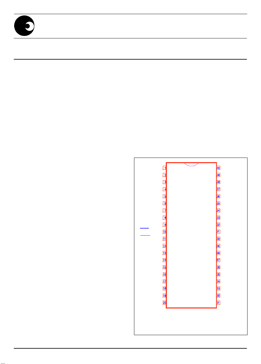
PIN CONNECTIONS
V
DD
VS[20]
VS[21]
VS[22]
VS[23]
SCK
MOSI
MISO
CE
RES
END
CLK
GND
M3
VI
NC
VR[0]
VR[1]
VR[2]
VR[3]
DR-00580
VS[19]
VS[18]
VS[17]
VS[16]
VS[15]
VS[14]
VS[13]
VS[12]
VS[11]
VS[10]
VS[9]
VS[8]
VS[7]
VS[6]
VS[5]
VS[4]
VS[3]
VS[2]
VS[1]
VS[0]
Package: DIP-40
1/14
4076 PDS039-SA8807-001 REV. C 11-09-95
Page 2
SA8807A
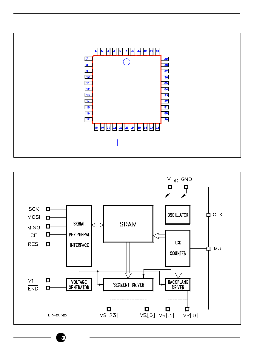
PIN CONNECTIONS
VS[14]
VS[13]
VS[11]
VS[12]
VS[9]
VS[10]
N.C.
VS[7]
VS[8]
VS[5]
VS[6]
BLOCK DIAGRAM
VS[15]
VS[16]
VS[17]
VS[18]
VS[19]
N.C.
V
DD
VS[20]
VS[21]
VS[22]
VS[23]
DR-00581
END
SCK
MOSICERES
MOSO
N.C.
CLK
Package: PLCC-44
VS[4]
VS[3]
VS[2]
VS[1]
VS[0]
N.C.
VR[3]
VR[2]
VR[1]
VR[0]
N.C.
GNDM3V1
2/14
sames
Page 3
SA8807A
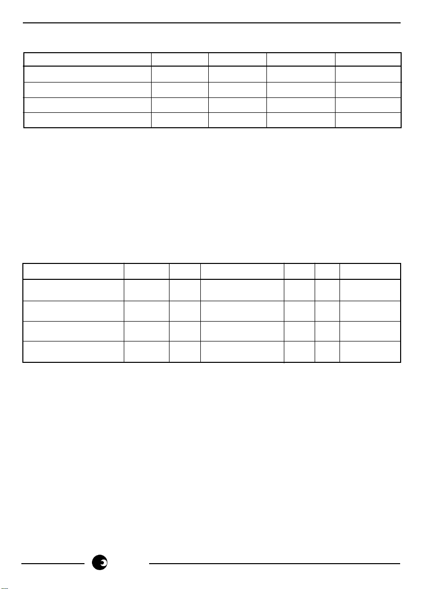
ABSOLUTE MAXIMUM RATINGS*
Parameter Symbol Min Max Unit
Supply Voltage VDD -V
Current on any pin I
Storage Temperature T
Operating Temperature T
PIN
STG
O
SS
-0.3 6.0 V
-150 +150 mA
-40 +125 °C
-25 +85 °C
* Stresses above those listed under “Absolute Maximum Ratings” may cause permanent
damage to the device. This is a stress rating only. Functional operation of the device
at these or any other condition above those indicated in the operational sections of this
specification, is not implied. Exposure to Absolute Maximum Ratings for extended
periods may affect device reliability.
ELECTRICAL CHARACTERISTICS
(Over the temperature range -10°C to +70°C#, VDD = 5V, VSS = 0V unless otherwise
specified.)
Parameter Symbol Min Typ Max Unit Condition
Supply Voltage VDD-V
Supply Current I
LCD ON Voltages V
LCD OFF Voltages V
#
Extended Operating Temperature Range available on request.
DD
ON
OFF
3.0 5.0 5.5 V
SS
VDD & V
1/3VDD & 2/3 V
SS
DD
sames
100 µA
V
V
3/14
Page 4
SA8807A
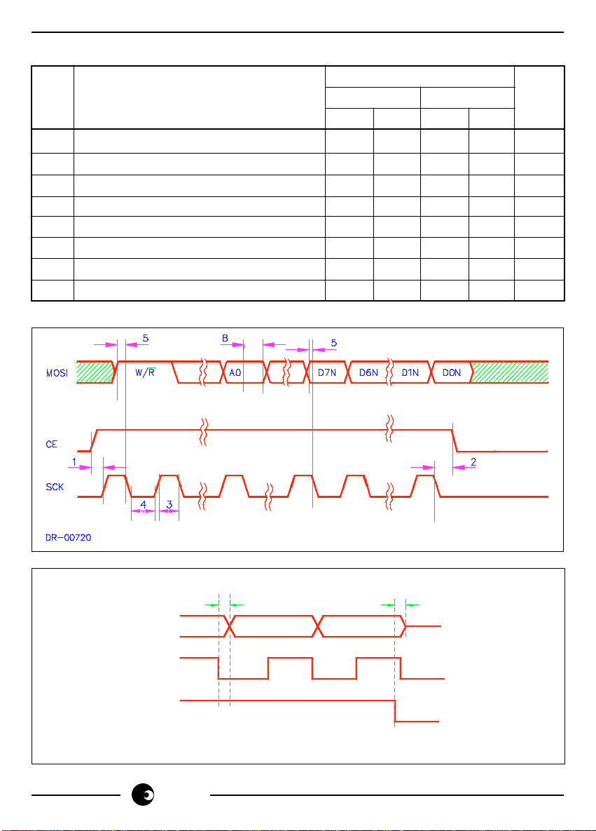
SERIAL INTERFACE TIMING
Ref
No
Characteristic VDD = 3.3V VDD = 5V Unit
Limits (All Types)
Min Max Min Max
1 Chip Enable set-up time 200 100 ns
2 Chip Enable clock hold time 250 125 ns
3 Clock width high 400 200 ns
4 Clock width low 400 200 ns
5 Data In to clock set-up time 200 100 ns
6 Clock to Data propagation delay 200 100 ns
7 Chip Disable to output high Z 200 100 ns
8 Data In after clock hold time 200 100 ns
4/14
MIS0
SCK
CE
DR-00846
sames
6
5.00
7
5.00
Page 5
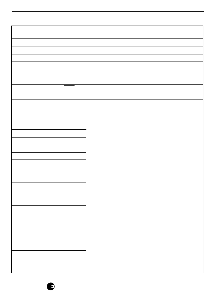
PIN DESCRIPTION
Pin Pin
Designation Description
PLCC-44 DIP-40
26 13 GND Ground
13 1 V
DD
Positive Supply Voltage
18 6 SCK (SPI) Serial clock input
19 7 MOSI (SPI) Master Out: Slave In
20 8 MISO (SPI) Master In: Slave Out
21 9 CE Chip Enable input
22 10 RES Reset input
23 11 END Divider Enable
25 12 CLK Oscillator or clock input
27 14 M3 3 / 4 Backplane enable input
28 15 V1 LCD Voltage input (Contrast)
35 21 VS[0] LCD segment driver outputs
36 22 VS[1]
37 23 VS[2]
38 24 VS[3]
39 25 VS[4]
40 26 VS[5]
41 27 VS[6]
42 28 VS[7]
43 29 VS[8]
1 30 VS[9]
2 31 VS[10]
3 32 VS[11]
4 33 VS[12]
5 34 VS[13]
6 35 VS[14]
7 36 VS[15]
8 37 VS[16]
9 38 VS[17]
10 39 VS[18]
11 40 VS[19]
SA8807A
sames
5/14
Page 6
SA8807A
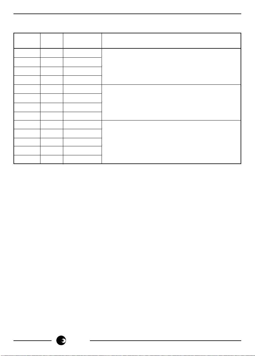
PIN DESCRIPTION (Continued)
Pin Pin
PLCC-44 DIP-40
Designation Description
14 2 VS[20] LCD segment driver outputs
15 3 VS[21]
16 4 VS[22]
17 5 VS[23]
30 17 VR[0] LCD row driver outputs
31 18 VR[1]
32 19 VR[2]
33 20 VR[3]
29 16 NC Not connected
12 NC
24 NC
34 NC
44 NC
FUNCTIONAL DESCRIPTION
The SA8807A is a CMOS Liquid Crystal Driver integrated circuit for displays having 3 or
4 track multiplexed backplanes and up to 96 LCD segments.
Data exchange is performed through a Serial Peripheral Interface (SPI).
1. Serial Peripheral (SPI) Interface
The SPI Interface is a 4 wire interface.
The device transmits the data to the Master via MISO (Master In, Slave Out).
Data from the Master is received through MOSI (Master Out, Slave In). The data
is always synchronised to the Serial Clock (SCK), which is supplied from the Master.
CE is a active high signal, the rising edge defining the start of a transfer procedure.
The transfer procedure is terminated with the falling edge of CE.
Diagram 1 illustrates the relationships between Clock, Data and Chip Enable
signals.
The SA8807A determines the clock polarity during the low to high transition of the
CE signal.
6/14
sames
Page 7
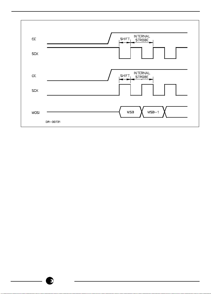
Diagram 1
2. Addressing and Read/Write Mode Select
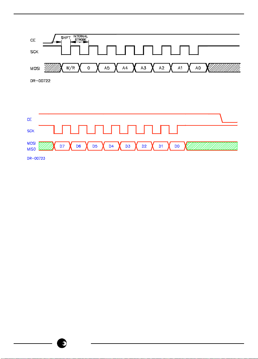
To access the SA8807A, a control byte has to be received first (after CE goes
active). This byte contains the information to initiate either a Read or Write mode
and an address.
SA8807A
The following bytes contain data until CE becomes inactive.
Address/Control Byte: The Address and Control Byte is the first byte sent after
CE goes active. To send another address, CE must first go inactive before going
active again. If the CE remains high, the device automatically increments the
address, for the following byte.
W/R = "1"
One or more write cycles to be sent.
W/R = "0"
Inititates one or more read cycles.
A5 - A0:
Address 5 to Address 0 selects the 6-bit HEX Address of RAM. (See LCD Character
Mapping)
SCK may be either polarity.
sames
7/14
Page 8
SA8807A
Read/Write Data: The Read/Write Data follows the Address/Control byte.
SCK may be either polarity.
8/14
sames
Page 9
3. LCD Display
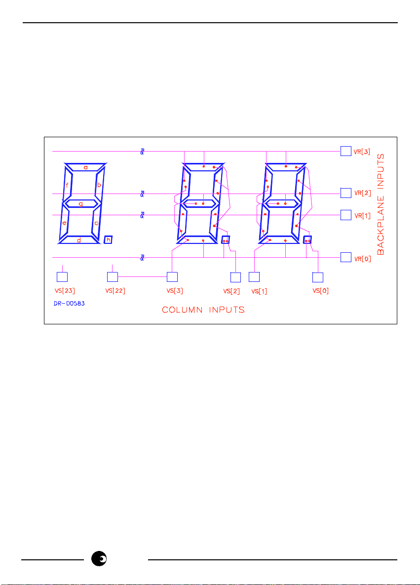
The SA8807A LCD driver is capable of driving a 3 or 4 backplane, 12 digit (7
segment) display, plus decimal points.
In the case of a 4 back plane display, typically the most significant digit is addressed
by columns VS[22] and VS[23] and the least significant digit, by VS[0] and VS[1].
The display segments addressed via the column outputs are given in a typical
configuration below:
SA8807A
The data in memory is constantly being displayed on the liquid crystal display. New
data is displayed as soon as it is latched into memory.
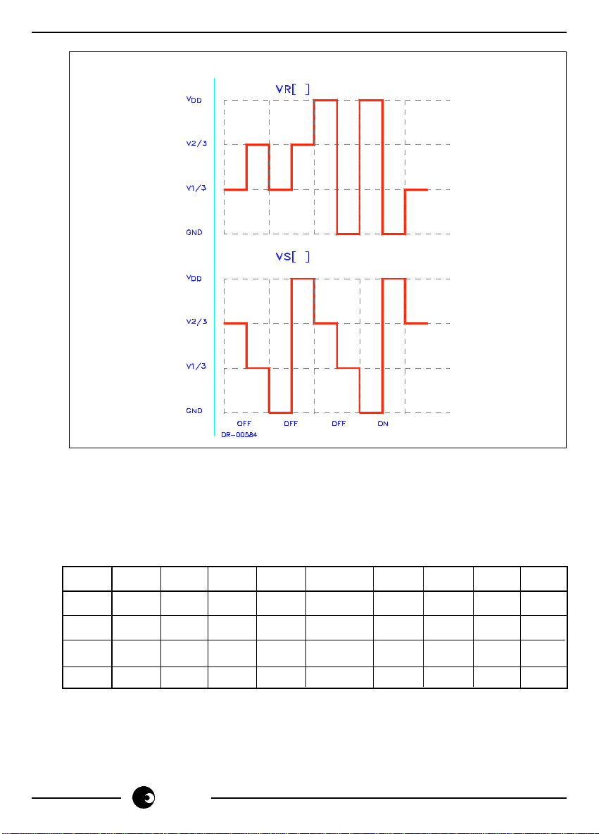
A segment is switched on when the corresponding difference between backplane
VR[ ] and segment VS[ ] outputs is VDD, and switched off when switched to 1/3 VDD.
The voltage is alternated to avoid a DC voltage on the LCD (See Diagram 2).
The backplane multiplex rate is determined by the clock/oscillator frequency on the
CLK input.
sames
9/14
Page 10
SA8807A
Diagram 2: LCD Driving Signals
4. LCD Character Mapping
The device contains 12 x 8 bit display memory. Each byte is divided into 2 x 4 bits,
for driving two adjacent segment outputs.
The lower four bits (3, 2, 1 & 0) contain the data for segments VS[0], VS[2], ......
VS[20] and VS[22]. The upper four bits (7, 6, 5 & 4) contain the data segments
VS[1], VS[3], ...... VS[21] and VS[23].
SEG VS[0] VS[1] VS[2] VS[3] ........ VS[20] VS[21] VS[22] VS[23]
VR[0] 0-0 0-4* 1-0 1-4 ........ 10-0 10-4 11-0 11-4
VR[1] 0-1 0-5 1-1 1-5 ........ 10-1 10-5 11-1 11-5
VR[2] 0-2 0-6 1-2 1-6 ........ 10-2 10-6 11-2 11-6
VR[3] 0-3 0-7 1-3 1-7 ........ 10-3 10-7 11-3 11-7
Note: A '1' switches the corresponding segment on.
* The address number and bit number of the byte is given, e.g. 0-4 is address 0 and
bit 4 (LSB).
In 3-backplane mode, data corresponsing to VR[3] (bit 3 and 7) is unused.
10/14
sames
Page 11

SA8807A
5. On-Chip LCD Voltage Divider Disable
The integrated divider for the LCD voltages can be disabled by applying a high level
on the EN input (EN = 1).
6. Contrast Setting
The contrast may be adjusted by applying an external LCD voltage on input V1, with
the internal voltage divider activated.
7. Oscillator
The on-chip oscillator circuit requires one external capacitor for operation. The
capacitor value is calculated as follows:
C = 7µF.1Hz/f
f = Required oscillator frequency
The backplane multiplex rate is f/8 for 4-backplane mode and f/6 for 3-backplane
mode.
TYPICAL APPLICATION
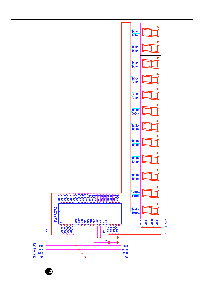
The Application Circuit (Figure 1) shows the connections for a typical application when
using a 12 digit (7 segment) display, plus decimal points.
sames
11/14
Page 12
SA8807A
Figure 1: LCD Driver Application
12/14
sames
Page 13

ORDERING INFORMATION
Part Number Package
SA8807APA DIP-40
SA8807AFA PLCC-44
SA8807A
sames
13/14
Page 14

SA8807A
Disclaimer: The information contained in this document is confidential and proprietary to South African Micro-
Electronic Systems (Pty) Ltd ("SAMES") and may not be copied or disclosed to a third party, in whole or in part,
without the express written consent of SAMES. The information contained herein is current as of the date of
publication; however, delivery of this document shall not under any circumstances create any implication that the
information contained herein is correct as of any time subsequent to such date. SAMES does not undertake to
inform any recipient of this document of any changes in the information contained herein, and SAMES expressly
reserves the right to make changes in such information, without notification, even if such changes would render
information contained herein inaccurate or incomplete. SAMES makes no representation or warranty that any
circuit designed by reference to the information contained herein, will function without errors and as intended by
the designer.
Any Sales or technical questions may be posted to our e-mail address below:
[email protected]
For the latest updates on datasheets, please visit out web site:
http://www.sames.co.za
South African Micro-Electronic Systems (Pty) Ltd
P O Box 15888, 33 Eland Street,
Lynn East, 0039 Koedoespoort Industrial Area,
Republic of South Africa, Pretoria,
Republic of South Africa
Tel: 012 333-6021 Tel: Int +27 12 333-6021
Fax: 012 333-8071 Fax: Int +27 12 333-8071
14/14
sames
 Loading...