

Page 1
INTEGRATED CIRCUITS
SA9504
Dual-band, PCS(CDMA)/AMPS
LNA and downconverter mixers
Preliminary specification
Supersedes data of 1999 Aug 24
1999 Oct 28
Page 2
Philips Semiconductors Preliminary specification
Dual-band, PCS(CDMA)/AMPS
LNA and downconverter mixers
DESCRIPTION
The SA9504 is an integrated receiver front-end for 900 MHz Cellular
(AMPS) and 1.9 GHz PCS (CDMA) phones. This dual-band receiver
circuit has low noise amplifiers and downconverters for both bands,
and provides an elegant solution for RF-to-IF conversion.
The two cascode LNAs have been designed to provide high gain
with very low noise figures and high linearity. The downconverter
portion is based on the Philips SA9502. There are two individual
mixer blocks, each optimized for low noise figure and high linearity.
The whole circuit is designed for low power consumption, high
performance, and is compatible with the requirements for Cellular
(AMPS) and PCS (CDMA) handsets.
The circuit has been designed in our advanced QUBiC3 BiCMOS
process with 30 GHz f
FEATURES
LNA typical performance
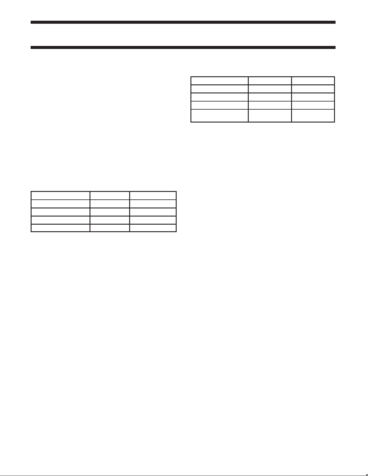
PARAMETER Cellular LNA PCS (CDMA) LNA
Gain (dB) 16.5 14.8
Noise figure (dB) 1.6 2
Input IP3 (dBm) –2 1
Current (mA) 4.9 4.9
•LNAs for both Cellular (AMPS) and PCS (CDMA) bands
•High gain, low noise figure, high linearity performance
•Cascode output structure requiring no external matching
•Low power consumption, typical 4.9 mA
•Low voltage operation down to 2.7 volts
and 60 GHz f
T
MAX
.
SA9504
Downconverter typical performance
PARAMETER Cellular FM PCS (CDMA)
Gain (dB) 7.5 11.5
Nois e Figure ( dB) 10 9
Input IP3 (dBm) 5 4
Current (mA)
(Tx) LO output buffer off
•Separate, selectable IF outputs to suit FM and CDMA bandwidths
•Buffered Cellular and PCS LO inputs
•Integrated frequency doubler for PCS mixer LO
•Differential (Tx) LO output buffer (can be switched on or off)
•Low voltage operation down to 2.7 volts
•Mixers current consumption with (Tx) LO buffer on:
– Cellular FM: 17.4 mA
– PCS: 27.6 mA
•Low standby current in sleep mode: <50 µA
•Small LQFP32 package
APPLICATIONS
•800 MHz analog FM and receivers
•1.9 GHz PCS (CDMA) digital receivers
•Supports dual-band operation
•Digital mobile communications equipment
•Portable, low power radio equipment
6.9 17
1999 Oct 28
2
Page 3
Philips Semiconductors Preliminary specification
PARAMETER
TEST CONDITIONS
UNIT
Dual-band, PCS(CDMA)/AMPS
LNA and downconverter mixers
BLOCK DIAGRAM
RF_PCS
SA9504
RF_CEL
RX BPF
Fo = 1960 MHz
BW = 60 MHz
PCS_INPCS_OUT
SA9504
2
PCS IF BPF
2
2
×2
2
2
CELLULARPCS
2
PCS_IF
FM_IF
2
21
BW = 1.23MHz
FM IF BPF
BW = 30kHz
MODE
SELECT
LOGIC
4
LO_X2_EN
PCS/CELLULAR
S0
S1
SR02107
CEL_OUT
CEL_IN
RX BPF
Fo = 881.5MHz
BW = 25 MHz
BIAS
CTRL
V
CC
2
LO_OUT
1
LO_ENABLE CEL
LO_IN
1
PCS
LO_IN
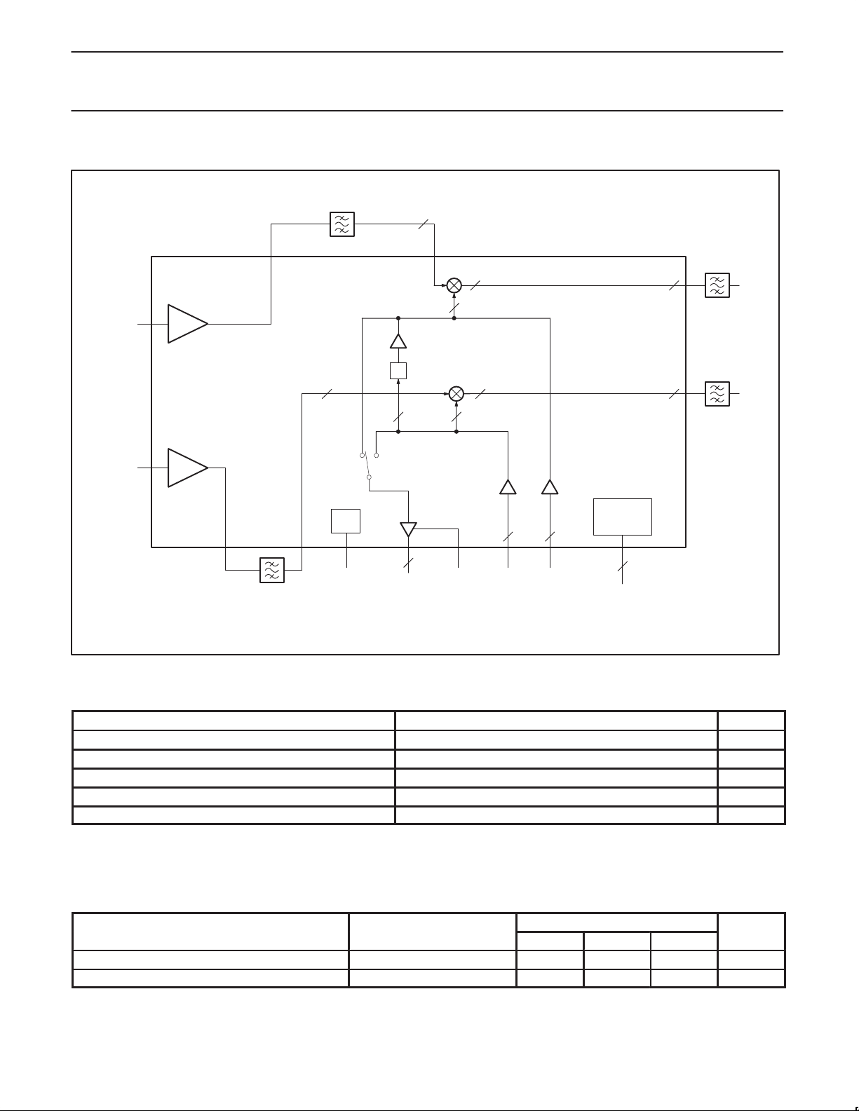
Figure 1. SA9504 Block Diagram
ABSOLUTE MAXIMUM RATINGS
PARAMETER
1
RATINGS UNIT
Supply voltage (VCC) –0.3 to +3.6 V
Logic input voltage –0.3 to VCC+0.3 V
Maximum power input +20 dBm
Power dissipation (T
= 25°C) 800 mW
amb
Storage temperature range –65 to +150 °C
NOTES:
1. Stresses beyond those listed may cause permanent damage to the device. These are stress ratings only and functional operation of the
device at these or any other conditions beyond those indicated under “Recommended Operating Conditions” is not implied. Exposure to
absolute-maximum-rated-conditions for extended periods may affect device reliability.
RECOMMENDED OPERATING CONDITIONS
LIMITS
MIN TYP MAX
Supply voltage (VCC) 2.7 2.85 3.3 V
Operating ambient temperature range (T
) –40 +85 °C
amb
1999 Oct 28
3
Page 4

Philips Semiconductors Preliminary specification
Dual-band, PCS(CDMA)/AMPS
LNA and downconverter mixers
FUNCTIONAL DESCRIPTION
Mode selection
The SA9504 has several modes of operation for which the selection
logic is defined in Table 1. Different mode selections require different
portions of the circuit to be active. Modes from unlisted combinations
of logic pins are not permitted. The LNA and downconverter together
can be programmed to operate in the PCS or cellular bands using
the PCS/CEL logic input pin.
In order for the SA9504 to function correctly, a reset must be applied
on first power-up. The whole circuit (LNAs and mixers) is powered
down when control lines S0 and S1 are simultaneously held HIGH.
An internal reset is applied upon releasing the circuit from
power-down (on taking S0 = S1 from HIGH to LOW).
LNA
The SA9504 has two LNAs, one for cellular FM, and one for PCS
(CDMA). The LNAs have been designed for high gain, low noise
figure and good linearity with low power consumption. External
components can be used to match the LNA inputs for the Cellular
and PCS bands. The LNAs employ a cascode output structure
allowing high gain and excellent reverse isolation. The LNA outputs
are internally matched to drive 50Ω external loads. The input and
output return loss of better than 10 dB can be achieved in all modes.
Downconverter
The SA9504 has two mixers, one for Cellular FM, and one for PCS
(CDMA). Each mixer is individually optimized for its specific
SA9504
requirements. The Cellular FM mixer has a common single-ended
RF input. The PCS mixer’s RF input port is differential, and requires
an external balun when used with a single-ended source. Both the
PCS and the Cellular mixer RF inputs should be AC coupled.
Local oscillator drive for the mixers is provided through pins
CEL LO_IN and/or PCS LO_IN. The local oscillator inputs are
single-ended, AC-coupled. The CEL LO_IN signal is internally
buffered to drive the following:
– (Tx) LO output buf fer,
– cellular FM mixer,
– PCS LO frequency doubler.
In the PCS mode, mixer LO drive can be either direct (PCS LO_IN)
or through the frequency doubler after CEL LO_IN. The mixer local
oscillator signal is made available externally via the (Tx) LO output
buffer for potential use elsewhere in the radio. For example, this
signal typically can be used with the transmitter circuitry. The
(Tx) LO output buffer can be powered down independently, using
the (Tx) LO_ENABLE logic input. The (Tx) LO output buffer has
open collector differential outputs which should be externally biased
to power supply rail.
The PCS and Cellular FM mixers have open collector differential IF
outputs. The differential IF outputs must be biased at the supply
voltage through external inductors that may also be part of the
matching circuit to the SAW filter .
1999 Oct 28
4
Page 5
Philips Semiconductors Preliminary specification
(Tx) LO
SYMBOL
PARAMETER
CONDITIONS
UNIT
Dual-band, PCS(CDMA)/AMPS
LNA and downconverter mixers
MODE SELECT LOGIC AND
DC CHARACTERISTICS
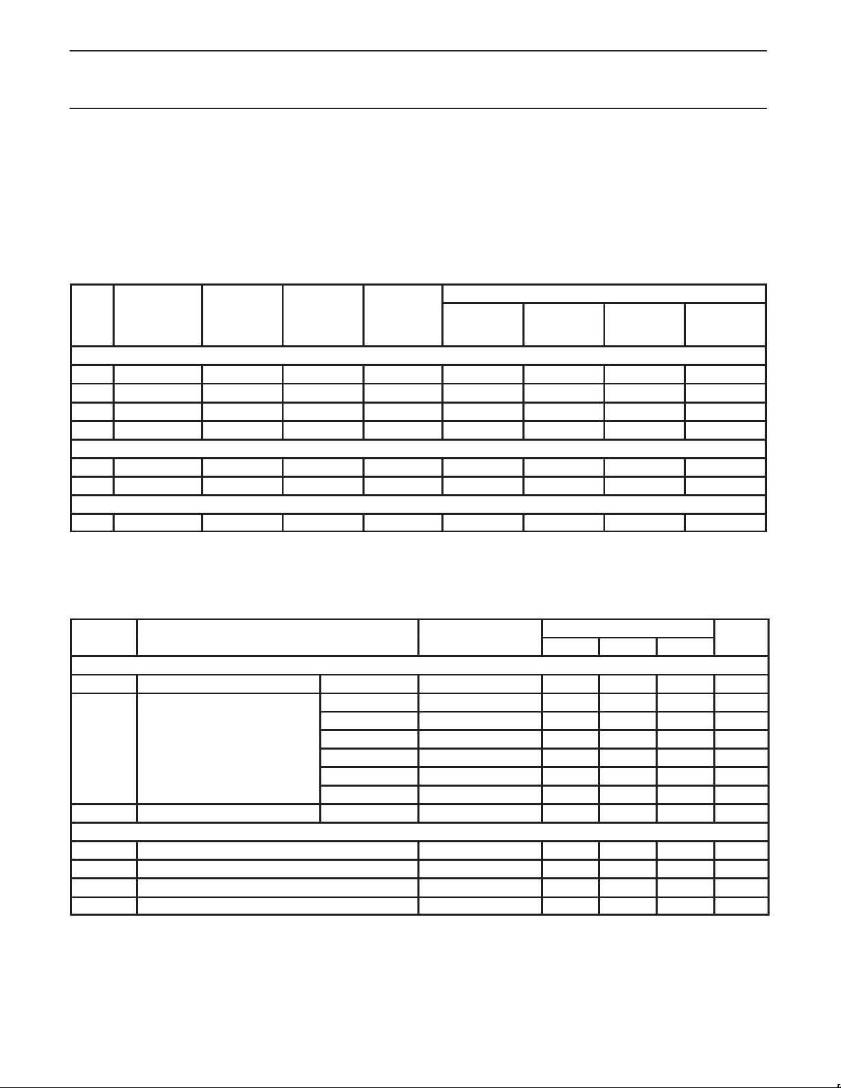
The SA9504 chip has several modes of operation for which the
selection logic is defined in the following table. Different mode
selections require different portions of the circuit to be active. Modes
from unlisted combinations of logic pins, are not valid.
Table 1. Mode logic definition for LNA and Downconverter mixers
MODES
PCS (CDMA)
1 PCS1 On 2 GHz Off 0 1 0 1
2 PCS1 Idle Off — Off 0 1 0 0
3 PCS2 On 2 GHz On 0 1 1 1
4 PCS2 Idle Off — On 0 1 1 0
Cellular FM
5 FM On 1 GHz Off 0 0 0 1
6 FM Idle Off — Off 0 0 0 0
Power Down
7 Sleep
NOTES:
x = Don’t care
1. The device will be in the Power Down mode (sleep) when both control lines S0 and S1 are held HIGH simultaneously.
1
(Tx) LO
BUFFER
x x Off 1 x x x
BUFFER
OUTPUT
LO FREQ.
DOUBLER
POWER-UP PROCEDURE
In order for the SA9504 to function correctly as given in Table 1, the
circuit must be reset on power-up as follows:
To apply a reset, both S0 and S1 should be held HIGH
simultaneously (hold time 100 ns minimum), and then released to a
LOW state upon initially powering up the device.
LOGIC INPUT PINS
POWER
DOWN
S0 = S1
1
PCS/CEL
LO X2
ENABLE
SA9504
(Tx) LO
ENABLE
DC CHARACTERISTICS
VCC = 3.3 V; T
Power supply
V
CC
I
CC
I
CC(PD)
Logic inputs (LO_ENABLE, PCS/CEL, S0, S1, LO_X2_EN pins)
V
IH
V
IL
I
IH
I
IL
= +25 °C
amb
Supply voltage all modes 2.7 2.85 3.3 V
Supply current
Supply current in power down Sleep 1 50 µA
HIGH level input voltage range At logic 1 0.5V
LOW level input voltage range At logic 0 –0.3 0.2V
HIGH level input bias current pins at VCC – 0.4 V –5 0 5 µA
LOW level input bias current pins at 0.4 V –5 0 5 µA
PCS1 mode 32.5 37.4 mA
PCS1 Idle mode 21.9 25.2 mA
PCS2 mode 36.9 42.4 mA
PCS2 Idle mode 26.3 30.2 mA
FM mode 22.3 25.6 mA
FM Idle mode 11.8 13.8 mA
LIMITS
MIN TYP MAX
CC
VCC+0.3 V
CC
V
1999 Oct 28
5
Page 6
Philips Semiconductors Preliminary specification
in ut isolation
and without doubler. 0 dBm LO in, (Tx) LO
SPECIFICATION
CONDITIONS
UNIT
Dual-band, PCS(CDMA)/AMPS
SA9504
LNA and downconverter mixers
LNA
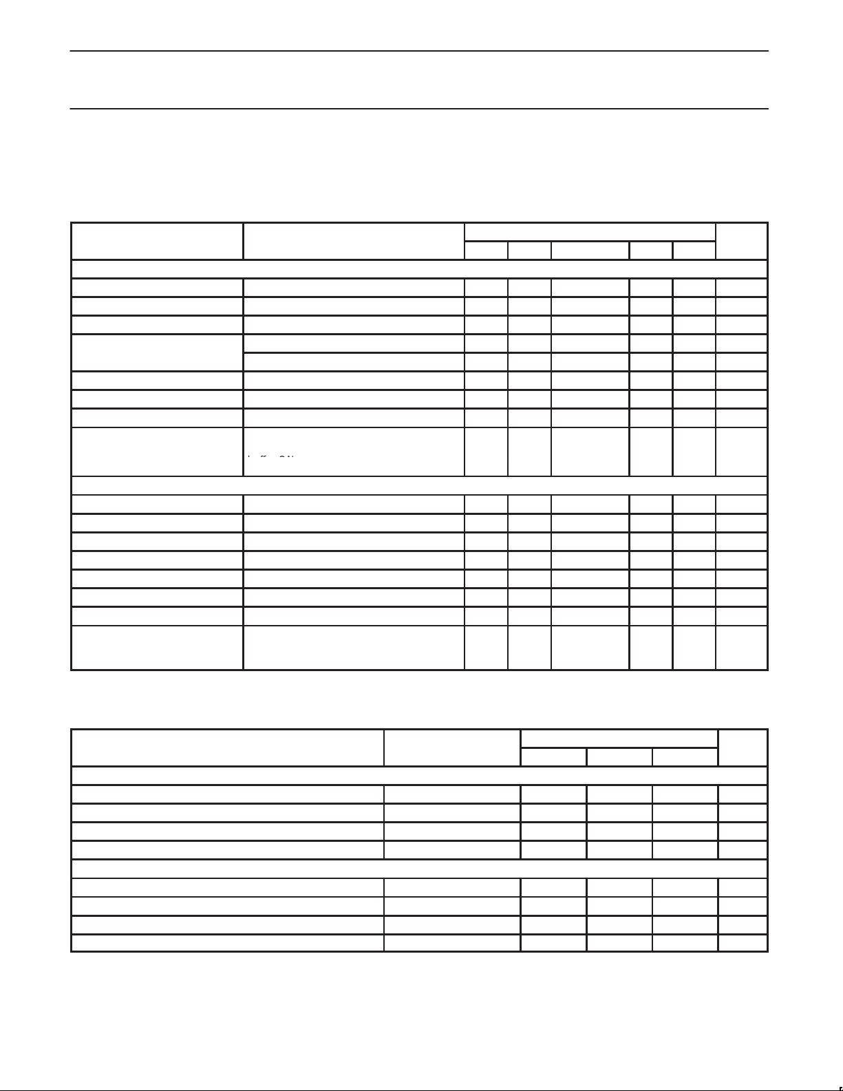
AC ELECTRICAL CHARACTERISTICS
VCC = 2.7 V; T
Cellular band LNA
RF input frequency range 869 894 MHz
Gain 15.5 16.5 17.5 dB
Noise Figure 1.6 1.9 dB
Input IP3
S11 With external matching –10 dB
S22 –15 dB
S12 –40 dB
LO (input and output) to LNA
input isolation
All modes
PCS band LNA
RF input frequency range 1810 1990 MHz
Gain 13.8 14.8 16 dB
Noise Figure 2.0 2.4 dB
Input IP3 2 tones of –30 dBm each, ∆f=800 kHz 0 1.5 dBm
S11 With external matching –9 dB
S22 –12 dB
S12 –40 dB
LO (input and Output) to LNApLO single-ended in, single-ended out, with
= 25°C
amb
PARAMETER TEST CONDITIONS
2 tones of –30 dBm each, ∆f=60 kHz –7 –6 dBm
2 tones of –30 dBm each, ∆f=800 kHz –3 –1.5 dBm
LO single-ended in, single-ended out, with
and without doubler. 0 dBm LO in, (Tx) LO
buffer ON.
MIN
–3σ
LIMITS
TYP +3σ MAX
40 dB
36 dB
UNIT
buffer ON.
TYPICAL LNA SPECIFICATIONS WITH TEMPERATURE VARIATION A T –40°C AND +85°C
VCC = 2.7 V
TEMPERATURE
–40°C +25°C +85°C
Cellular band LNA
Supply current variation –100 0 –100 µA
Gain variation 1 0 –1 dB
Noise Figure variation –0.3 0 0.3 dB
Input IP3 variation ∆f = 60 kHz –0.35 0 0.3 dBm
PCS band LNA
Supply current variation –40 0 –40 µA
Gain variation 0.8 0 –1 dB
Noise Figure variation –0.4 0 0.4 dB
Input IP3 variation 0.9 0 –1 dBm
1999 Oct 28
6
Page 7
Philips Semiconductors Preliminary specification
PARAMETER
TEST CONDITIONS
UNIT
Dual-band, PCS(CDMA)/AMPS
SA9504
LNA and downconverter mixers
DOWNCONVERTER
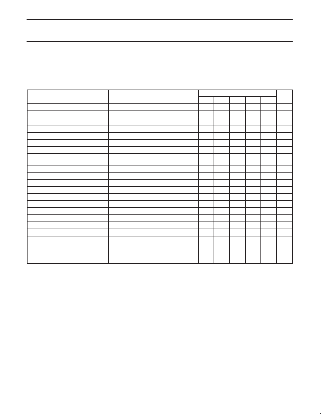
AC ELECTRICAL CHARACTERISTICS
VCC = 2.7 V; T
f
= 881 MHz, fLO = 966.4 MHz, fIF = 85.4 MHz, output differential load of 850Ω for FM.
RF
Cellular band downconverter
RF input frequency range 869 894 MHz
LO input frequency range 950 1030 MHz
IF output frequency range 50 300 MHz
IF Output Load Impedance Single-ended, with external balun 850 Ω
Conversion Gain 6.5 7.5 8.2 dB
Noise Figure Single sideband Noise Figure 10 11 dB
Input IP3 P1, P2 = –24 dBm.
RF Input Return Loss ZS=50Ω with external matching 11.0 dB
LO Input Return Loss ZS=50Ω 10.0 dB
(Tx) LO Output Return Loss ZS=50Ω 8.0 dB
LO Input Power Range –9 –6 0 dBm
(Tx) LO Output Power Range ZL=50Ω single-ended; (Tx) LO buffer ON. –6 –3 0 dBm
LO (Input and Output) to RF Leakage Single-ended in, single-ended out. –30 dBm
LO (Input and Output) to IF Leakage Single-ended in, differential out. –20 dBm
RF to LO (Input) Isolation Single-ended in, single-ended out 30 dB
RF to IF Isolation Single-ended in, differential out 10 dB
(Tx) LO Output to LO Input Isolation Single-ended in, differential out 30 dB
Leakage conversion gain f1 = fRX ± 40 MHz at LNA input.
= 25°C, Plo= –3 dBm.
amb
Tone spacing = 60 kHz
P1 = – 70 dBm.
Measured through conversion gain in
stop-band, without SAW filters being
connected. Ports terminated with 50Ω.
MIN
LIMITS
TYP
–3s
5.0 dBm
–40 dBc
+3s
MAX
1999 Oct 28
7
Page 8

Philips Semiconductors Preliminary specification
PARAMETER
TEST CONDITIONS
UNIT
SPECIFICATION
UNIT
Dual-band, PCS(CDMA)/AMPS
SA9504
LNA and downconverter mixers
AC ELECTRICAL CHARACTERISTICS (continued)
VCC = 2.7 V; T
f
= 1960 MHz, fLO = 1750 MHz, fIF = 210 MHz, output differential load of 1 kΩ for PCS.
RF
PCS Downconverter
RF input frequency range 1810 1990 MHz
LO input frequency range
IF output frequency range 50 300 MHz
IF Output Load Impedance Differential 1000 Ω
Conversion Gain 10.5 11.5 12.5 dB
Noise Figure
Input IP3 P1, P2 = –30 dBm
RF Input Return Loss ZS = 50Ω, with external matching 10 dB
LO Input Return Loss ZS = 50Ω 10 dB
(Tx) LO Output Return Loss ZS = 50Ω 8 dB
LO Input Power Range –9 –6 0 dBm
(Tx) LO Output Power Range ZL = 50Ω single-ended; (Tx) LO buffer ON –10 –9 –6 dBm
LO (input and Output) to RF Leakage Single-ended in, single-ended out,
LO (input and Output) to IF Leakage Single-ended in, differential out,
RF to LO (Input) Isolation Single-ended in, single-ended out,
RF to IF Isolation Single-ended in, differential out 20 dB
(Tx) LO Output to LO Input Isolation Single-ended in, differential out, with doubler 30 dB
Leakage conversion gain f1 = fRX ± 80 MHz at LNA input.
= 25°C, Plo= –3 dBm.
amb
LIMITS
MIN
without doubler 1720 2120 MHz
with doubler 860 1050 MHz
SSB NF, low side LO (fLO = 1750 MHz) 9.0 10 dB
SSB NF, high side LO (fLO = 2170 MHz) 8.0 9 dB
Tone spacing = 800 kHz
with and without doubler
with and without doubler
with and without doubler
P1 = – 70 dBm.
Measured through conversion gain in
stop-band, without SAW filters being
connected. Ports terminated with 50Ω.
TYP
–3s
3 4 dBm
30 dB
–40 dBc
MAX
+3s
–35 dBm
–35 dBm
TYPICAL DOWNCONVERTER SPECIFICA TIONS WITH TEMPERATURE V ARIATION FROM –40°C TO +85°C
VCC = 2.7 V
TEMPERATURE
–40°C +25°C +85°C
Cellular band downconverter
Conversion Gain Variation 1 0 –1 dB
IP3 Variation –4 0 +1 dB
Noise Figure Variation –1.5 0 1.5 dB
PCS band downconverter
Conversion Gain Variation 1 0 –1 dB
IP3 Variation 0.5 0 –1 dB
Noise Figure Variation –1.5 0 0.8 dB
1999 Oct 28
8
Page 9

Philips Semiconductors Preliminary specification
Dual-band, PCS(CDMA)/AMPS
LNA and downconverter mixers
TYPICAL PERFORMANCE CHARACTERISTICS
DC current consumption
PCS1 Mode Current
33
32.5
32
31.5
31
Current (mA)
30.5
30
2.50 3.00 3.50
VCC (V)
Figure 2. PCS1 Mode Current
PCS1 Mode Idle Current
22.5
22
21.5
Current (mA)
21
20.5
2.50 3.00 3.50
VCC (V)
–40°C
+25°C
+85°C
SR02125
–40°C
+25°C
+85°C
FM Mode Current
23
22.5
22
21.5
Current (mA)
21
2.50 3.00 3.50
VCC (V)
Figure 6. FM Mode Current
FM Mode Idle Current
12
11.8
11.6
11.4
11.2
Current (mA)
11
2.50 2.70 2.90 3.10 3.30 3.50
(V)
V
CC
SA9504
–40°C
+25°C
+85°C
SR02124
–40°C
+25°C
+85°C
Figure 3. PCS1 Mode Idle Current
PCS2 Mode Current
37
36.5
36
Current (mA)
35.5
35
2.50 3.00 3.50
VCC (V)
Figure 4. PCS2 Mode Current
PCS2 Mode Idle Current
27
26.5
26
Current (mA)
25.5
25
2.50 2.70 2.90 3.10 3.30 3.50
(V)
V
CC
Figure 5. PCS2 Mode Idle Current
SR02123
–40°C
+25°C
+85°C
SR02127
–40°C
+25°C
+85°C
SR02128
Figure 7. FM Mode Idle Current
Sleep Mode Current
3
2.5
2
1.5
1
Current (uA)
0.5
0
2.50 2.70 2.90 3.10 3.30 3.50
VCC (V)
Figure 8. Sleep Mode Current
SR02122
–40°C
+25°C
+85°C
SR02121
1999 Oct 28
9
Page 10

Philips Semiconductors Preliminary specification
Dual-band, PCS(CDMA)/AMPS
LNA and downconverter mixers
LNA characteristics
Cellular LNA Gain @ 881 MHz vs. V
18.0
17.0
GAIN (dB)
16.0
15.0
2.50 2.70 2.90 3.10 3.30 3.50
VCC (V)
Figure 9.
PCS LNA Gain @ 1960 MHz vs. V
16.5
15.5
14.5
GAIN (dB)
13.5
2.50 2.70 2.90 3.10 3.30 3.50
VCC (V)
Figure 10.
CC
CC
–40°C
+25°C
+85°C
SR02129
–40°C
+25°C
+85°C
SR02130
Cellular LNA Input IP3 @ 881 MHz vs. V
–1
–1.2
–1.4
–1.6
Input IP3 (dB)
–1.8
–2
2.50 2.70 2.90 3.10 3.30 3.50
VCC (V)
Figure 12.
PCS LNA Input IP3 @ 1960 MHz vs. V
3.5
3
2.5
2
Gain (dB)
1.5
1
2.50 2.70 2.90 3.10 3.30 3.50
VCC (V)
Figure 13.
SA9504
CC
–40°C
+25°C
+85°C
SR02131
CC
–40°C
+25°C
+85°C
SR02132
LNA Noise Figure vs. Temerature
2.4
2.2
2
1.8
1.6
NF in dB
1.4
1.2
1
VCC = 2.85 V
–40°C
+25°C +85°C
AMBIENT TEMPERATURE
Figure 11.
CEL–1
PCS–1
SR02133
LNA Noise Figure vs. V
Temp. = 25°C
2.4
2.2
2
1.8
1.6
NF in dB
1.4
1.2
1
2.50 2.70 2.90 3.10 3.30 3.50
VCC (V)
Figure 14.
CC
CEL–1
PCS–1
SR02134
1999 Oct 28
10
Page 11

Philips Semiconductors Preliminary specification
Dual-band, PCS(CDMA)/AMPS
LNA and downconverter mixers
Cellular Band Downconverter – Conversion Gain
Conversion Gain vs. Frequency , Cellular FM
8.0
7.5
7.0
6.5
CONVERSION GAIN (dB)
6.0
850 860 870 880 890 900 910
Conversion Gain vs. LO Input Power, Cellular FM
8.0
7.5
7.0
6.5
CONVERSION GAIN (dB)
6.0
–15 –12 –9 –6 –3 0
Temp. = 25°C
FREQUENCY (MHz)
Figure 15.
Temp. = 25°C
LO (dBm)
Figure 16.
2.70V
3.30V
SR02135
2.70V
3.30V
SR02137
SA9504
Conversion Gain vs. Frequency, Cellular FM
10.0
9.0
8.0
7.0
6.0
CONVERSION GAIN (dB)
5.0
850 860 870 880 890 900 910
Conversion Gain vs. LO Input Power, Cellular FM
10.0
9.0
8.0
7.0
6.0
CONVERSION GAIN (dB)
5.0
–15 –12 –9 –6 –3 0
VCC = 2.70 V
FREQUENCY MHz)
Figure 18.
VCC = 2.70 V
LO (dBm)
Figure 19.
–40°C
+25°C
+85°C
SR02136
–40°C
+25°C
+85°C
SR02138
Conversion Gain vs. RF Input Power, Cellular FM
Temp. = 25°C
8.0
7.5
7.0
6.5
CONVERSION GAIN (dB)
6.0
–23 –22 –21 –20 –19 –18 –17 –16
RF INPUT POWER (dBm)
Figure 17.
2.70V
3.30V
SR02139
Conversion Gain vs. RF Input Power, Cellular FM
VCC = 2.70 V
10.0
9.0
8.0
7.0
6.0
CONVERSION GAIN (dB)
5.0
–23 –22 –21 –20 –19 –18 –17 –16
RF INPUT POWER (dBm)
Figure 20.
–40°C
+25°C
+85°C
SR02140
1999 Oct 28
11
Page 12

Philips Semiconductors Preliminary specification
Dual-band, PCS(CDMA)/AMPS
LNA and downconverter mixers
PCS Downconverter (Direct LO) – Conversion Gain
Conversion Gain vs. Frequency , PCS1 Mixer
12.0
11.5
11.0
10.5
10.0
CONVERSION GAIN (dB)
1920 1940 1960 1980 2000
Conversion Gain vs. LO Input Power, PCS1 Mixer
12.0
11.5
11.0
10.5
CONVERSION GAIN (dB)
10.0
–15 –12 –9 –6 –3 0
Temp. = 25°C
FREQUENCY (MHz)
Figure 21.
Temp. = 25°C
LO (dBm)
Figure 22.
2.70V
3.30V
SR02141
2.70V
3.30V
SR02143
Conversion Gain vs. Frequency, PCS1 Mixer
VCC = 2.70 V
14.0
13.0
12.0
11.0
10.0
9.0
CONVERSION GAIN (dB)
8.0
1920 1940 1960 1980 2000
FREQUENCY (MHz)
Figure 24.
Conversion Gain vs. LO Input Powr, PCS1 Mixer
VCC = 2.70 V
14.0
13.0
12.0
11.0
10.0
9.0
CONVERSION GAIN (dB)
8.0
–15 –12 –9 –6 –3 0
LO (dBm)
Figure 25.
SA9504
–40°C
+25°C
+85°C
SR02142
–40°C
+25°C
+85°C
SR02144
Conversion Gain vs. RF Input Power, PCS1 Mixer
Temp. = 25°C
12.0
11.5
11.0
10.5
CONVERSION GAIN (dB)
10.0
–28 –26 –24 –22 –20 –18 –16
RF INPUT POWER (dBm)
Figure 23.
2.70V
3.30V
SR02145
Conversion Gain vs. RF Input Power, PCS1 Mixer
VCC = 2.70 V
14.0
13.0
12.0
11.0
10.0
9.0
CONVERSION GAIN (dB)
8.0
–28 –26 –24 –22 –20 –18 –16
RF INPUT POWER (dBm)
Figure 26.
–40°C
+25°C
+85°C
SR02146
1999 Oct 28
12
Page 13

Philips Semiconductors Preliminary specification
Dual-band, PCS(CDMA)/AMPS
LNA and downconverter mixers
PCS Downconverter (LO Doubler) – Conversion Gain
Conversion Gain vs. Frequency , PCS2 Mixer
13.0
12.0
11.0
10.0
9.0
CONVERSION GAIN (dB)
1920 1940 1960 1980 2000
Conversion Gain vs. LO Input Power, PCS2 Mixer
11.50
11.00
10.50
10.00
9.50
–15 –12 –9 –6 –3 0
CONVERSION GAIN (dB)
Temp. = 25°C
FREQUENCY (MHz)
Figure 27.
Temp. = 25°C
LO (dBm)
Figure 28.
2.70V
3.30V
SR02147
2.70V
3.30V
SR02149
SA9504
Conversion Gain vs. Frequency, PCS2 Mixer
13.0
12.0
11.0
10.0
9.0
CONVERSION GAIN (dB)
1920 1940 1960 1980 2000
Conversion Gain vs. LO Input Power, PCS2 Mixer
13.00
11.00
9.00
7.00
5.00
CONVERSION GAIN (dB)
–15 –12 –9 –6 –3 0
VCC = 2.70 V
FREQUENCY (MHz)
Figure 30.
VCC = 2.70 V
LO (dBm)
Figure 31.
–40°C
+25°C
+85°C
SR02148
–40°C
+25°C
+85°C
SR02150
Conversion Gain vs. RF Input Power, PCS2 Mixer
Temp. = 25°C
12.00
11.50
11.00
10.50
10.00
CONVERSION GAIN (dB)
–28 –26 –24 –22 –20 –18 –16
RF INPUT POWER (dBm)
2.70V
3.30V
Figure 29.
SR02151
Conversion Gain vs. RF Input Power, PCS2 Mixer
VCC = 2.70 V
13.00
12.00
11.00
10.00
9.00
–28 –26 –24 –22 –20 –18 –16
CONVERSION GAIN (dB)
RF INPUT POWER (dBm)
Figure 32.
–40°C
+25°C
+85°C
SR02152
1999 Oct 28
13
Page 14

Philips Semiconductors Preliminary specification
Dual-band, PCS(CDMA)/AMPS
LNA and downconverter mixers
Cellular Band Downconverter – Input IP3
Input IP3 vs. LO Input Power, Cellular FM
9
8
7
6
5
INPUT IP3 (dBm)
4
–15 –12
Input IP3 vs. Frequency, Cellular FM
9.0
8.5
8.0
7.5
INPUT IP3 (dBm)
7.0
850 860 870 880 890 900 910
Temp. = 25°C
–9 –6 –3
LO (dBm)
Figure 33.
Temp. = 25°C
FREQUENCY (MHz)
Figure 34.
0
2.70V
3.30V
SR02154
2.70V
3.30V
SR02156
Input IP3 vs. LO Input Power, Cellular FM
VCC = 2.70 V
9
8
7
6
5
INPUT IP3 (dBm)
4
–15 –12 –9 –6 –3 0
LO (dBm)
Figure 36.
Input IP3 vs. Frequency, Cellular FM
VCC = 2.70 V
9.0
8.0
7.0
6.0
INPUT IP3 (dBm)
5.0
4.0
850 860 870 880 890 900 910
FREQUENCY (MHz)
Figure 37.
SA9504
–40°C
+25°C
+85°C
SR02155
–40°C
+25°C
+85°C
SR02157
Input IP3 vs. Temperature, Cellular FM
RF Frequency: 881 MHz
9.0
8.0
7.0
6.0
5.0
INPUT IP3 (dBm)
4.0
–50 –30 –10 10 30 50 70 90
AMBIENT TEMPERATURE (°C)
Figure 35.
2.7V
3.3V
SR02153
1999 Oct 28
14
Page 15

Philips Semiconductors Preliminary specification
Dual-band, PCS(CDMA)/AMPS
LNA and downconverter mixers
PCS Downconverter (Direct LO) – Input IP3
Input IP3 vs. LO Input Power, PCS1 Mixer
6
5
4
INPUT IP3 (dBm)
3
–15 –12 –9 –6 –3 0
Input IP3 vs. Frequency, PCS1 Mixer
7.00
6.00
5.00
4.00
INPUT IP3 (dBm)
3.00
1920 1940 1960 1980 2000
Temp. = 25°C
LO (dBm)
Figure 38.
Temp. = 25°C
FREQUENCY (MHz)
Figure 39.
2.70V
3.30V
SR02159
2.70V
3.30 V
SR02161
Input IP3 vs. LO Input Power, PCS1 Mixer
VCC = 2.70 V
6
5
4
INPUT IP3 (dBm)
3
–15 –12 –9 –6 –3 0
LO (dBm)
Figure 41.
Input IP3 vs. Frequency, PCS1 Mixer
VCC = 2.70 V
7.0
6.0
5.0
4.0
INPUT IP3 (dBm)
3.0
1920 1940 1960 1980 2000
FREQUENCY (MHz)
Figure 42.
SA9504
–40°C
+25°C
+85°C
SR02160
–40°C
+25°C
+85°C
SR02162
Input IP3 vs. Temperature, PCS1 Mixer
RF Frequency: 1960 MHz
6.00
5.00
4.00
INPUT IP3 (dBm)
3.00
–50 –30 –10 10 30 50 70 90
AMBIENT TEMPERATURE 〈°C)
Figure 40.
2.7V
3.3V
SR02158
1999 Oct 28
15
Page 16

Philips Semiconductors Preliminary specification
Dual-band, PCS(CDMA)/AMPS
LNA and downconverter mixers
PCS Downconverter (LO Doubler) – Input IP3
Input IP3 vs. LO Input Power, PCS2 Mixer
6
5
4
3
INPUT IP3 (dBm)
2
–15 –12
Input IP3 vs. Frequency, PCS2 Mixer
6.0
5.0
4.0
3.0
INPUT IP3 (dBm)
2.0
1920 1940 1960 1980 2000
Temp. = 25°C
–9 –6 –3
LO (dBm)
Figure 43.
Temp. = 25°C
FREQUENCY (MHz)
Figure 44.
0
2.70v
3.30v
SR02164
2.70V
3.30V
SR02166
Input IP3 vs. LO Input Power, PCS2 Mixer
VCC = 2.70 V
6
5
4
3
INPUT IP3 (dBm)
2
–15 –12 –9 –6 –3 0
LO (dBm)
Figure 46.
Input IP3 vs. Frequency, PCS2 Mixer
VCC = 2.70 V
6.0
5.0
4.0
3.0
INPUT IP3 (dBm)
2.0
1920 1940 1960 1980 2000
FREQUENCY (MHz)
Figure 47.
SA9504
–40°C
+25°C
+85°C
SR02165
–40°C
+25°C
+85°C
SR02167
Input IP3 vs. Temperature, PCS2 Mixer
RF Frequency: 1960 MHz
6.0
5.0
4.0
3.0
INPUT IP3 (dBm)
2.0
–50 –30 –10 10 30 50 70 90
AMBIENT TEMPERATURE (°C)
Figure 45.
2.7V
3.3V
SR02163
1999 Oct 28
16
Page 17

Philips Semiconductors Preliminary specification
Dual-band, PCS(CDMA)/AMPS
LNA and downconverter mixers
Downconverter Mixers Noise Figure
Noise Figure vs. VCC, Cellular FM
12
11
10
9
NOISE FIGURE (dB)
8
2.5 2.7 2.9 3.1 3.3 3.5
Noise Figure vs. VCC, PCS1 Mixer
11
10
9
8
NOISE FIGURE (dB)
7
2.5 2.7 2.9 3.1 3.3 3.5
LO = –3 dBm
VCC (Volts)
Figure 48.
LO = –3 dBm
V
(Volts)
CC
Figure 49.
–40°C
+25°C
+85°C
SR02168
–40°C
+25°C
+85°C
SR02170
Noise Figure vs. LO, Cellular FM
14
12
10
8
NOISE FIGURE (dB)
6
0 –3 –6 –9 –12 –15
Noise Figure vs. LO, PCS1 Mixer
13
12
11
10
9
NOISE FIGURE (dB)
8
7
0 –3 –6 –9 –12 –15
VCC = 3.3 V
LO (dBm)
Figure 51.
VCC = 3.30 V
LO (dBm)
Figure 52.
SA9504
–40°C
+25°C
+85°C
SR02169
–40°C
+25°C
+85°C
SR02171
Noise Figure vs. VCC, PCS2 Mixer
LO = –3 dBm
11
10
9
8
NOISE FIGURE (dB)
7
2.5 2.7 2.9 3.1 3.3 3.5
VCC (Volts)
Figure 50.
–40°C
+25°C
+85°C
SR02172
Noise Figure vs. LO, PCS2 Mixer
19
17
15
13
11
9
NOISE FIGURE (dB)
7
0 –3 –6 –9 –12 –15
VCC = 3.30 V
LO (dBm)
Figure 53.
–40°C
+25°C
+85°C
SR02173
1999 Oct 28
17
Page 18

Philips Semiconductors Preliminary specification
Dual-band, PCS(CDMA)/AMPS
LNA and downconverter mixers
Vcc
Vcc
SA9504
Vcc
Vcc
Vcc
Vcc
PCS/CEL
PCS_IN
PCS_INB
S0
S1
PCS_OUT
GND9
LO_X2_EN
Vcc
25
26
27
28
29
30
31
32
PCS_IF
PCS_IFB
23
24
1
2
Vcc1
GND1
NC
NC
21
22
3
4
GND2
RF_PCS
FM_IF
FM_IFB
19
20
5
6
GND3
GND4
LO_OUT
LO_OUTB
18
16
GND8
15
14
x2
SA9504
7
GND5
13
12
11
10
9
817
RF_CEL
CEL_LO_IN
PCS_LO
CEL_IN
GND7
GND6
CEL_OUT
LO_ENABLE
Vcc
1999 Oct 28
SR02105
Figure 54. Demonstration Board Diagram
18
Page 19

Philips Semiconductors Preliminary specification
Dual-band, PCS(CDMA)/AMPS
LNA and downconverter mixers
PINNING
S0
1
V
1
CC
2
GND1
RF_PCS
×2
3
4
GND2
5
GND3
6
GND4
7
GND5
8
RF_CEL
= FREQUENCY DOUBLER
Figure 55. Pin-Out Block Diagram
GND9
S1
PCS_OUT
LO_X2_EN
32313029282726
SA9504
×2
9
10111213141516
GND6
GND7
CEL_OUT
LO_ENABLE
CEL_IN
PCS_IN
PCS_INB
PCS_LO
CEL_LO_IN
PCS/CEL
25
24
23
22
21
20
19
18
17
GND8
PCS_IFB
PCS_IF
NC
NC
FM_IFB
FM_IF
LO_OUTB
LO_OUT
SR02106
SA9504
Table 2. Pin function definition
PIN NAME DESCRIPTION
1 VCC1 Power supply
2 GND1 Ground
3 RF_PCS PCS LNA input
4 GND2 Ground
5 GND3 Ground
6 GND4 Ground
7 GND5 Ground
8 RF_CEL Cellular LNA input
9 LO_ENABLE (Tx) LO buffer enable
10 CEL_OUT Cellular LNA output
11 GND6 Ground
12 GND7 Ground
13 CEL_IN Cellular RF mixer input
14 PCS_LO PCS LO input
15 CEL_LO_IN Cellular LO input
16 GND8 Ground
17 LO_OUT Non-inverting (Tx) LO output
18 LO_OUTB Inverting (Tx) LO output
19 FM_IF Non-inverting FM IF output
20 FM_IFB Inverting FM IF output
21 NC Do not connect
22 NC Do not connect
23 PCS_IF Non-inverting PCS IF output
24 PCS_IFB Inverting PCS IF output
25 PCS/CEL PCS and cellular band select
26 PCS_IN Non-inverting PCS RF mixer input
27 PCS_INB Inverting PCS RF mixer input
28 S0 Control signal S0
29 S1 Control signal S1
30 PCS_OUT PCS LNA output
31 GND9 Ground
32 LO_X2_EN LO frequency doubler enable
in PCS mode
1999 Oct 28
19
Page 20

Philips Semiconductors Preliminary specification
Dual-band, CDMA/AMPS LNA
and downconverter mixers
LQFP32: plastic low profile quad flat package; 32 leads; body 5 x 5 x 1.4 mm SOT401-1
SA9504
1999 Oct 28
20
Page 21

Philips Semiconductors Preliminary specification
Dual-band, CDMA/AMPS LNA
and downconverter mixers
SA9504
NOTES
1999 Oct 28
21
Page 22

Philips Semiconductors Preliminary specification
Dual-band, CDMA/AMPS LNA
and downconverter mixers
Data sheet status
Data sheet
status
Objective
specification
Preliminary
specification
Product
specification
Product
status
Development
Qualification
Production
Definition
This data sheet contains the design target or goal specifications for product development.
Specification may change in any manner without notice.
This data sheet contains preliminary data, and supplementary data will be published at a later date.
Philips Semiconductors reserves the right to make changes at any time without notice in order to
improve design and supply the best possible product.
This data sheet contains final specifications. Philips Semiconductors reserves the right to make
changes at any time without notice in order to improve design and supply the best possible product.
[1]
SA9504
[1] Please consult the most recently issued datasheet before initiating or completing a design.
Definitions
Short-form specification — The data in a short-form specification is extracted from a full data sheet with the same type number and title. For
detailed information see the relevant data sheet or data handbook.
Limiting values definition — Limiting values given are in accordance with the Absolute Maximum Rating System (IEC 134). Stress above one
or more of the limiting values may cause permanent damage to the device. These are stress ratings only and operation of the device at these or
at any other conditions above those given in the Characteristics sections of the specification is not implied. Exposure to limiting values for extended
periods may affect device reliability.
Application information — Applications that are described herein for any of these products are for illustrative purposes only. Philips
Semiconductors make no representation or warranty that such applications will be suitable for the specified use without further testing or
modification.
Disclaimers
Life support — These products are not designed for use in life support appliances, devices or systems where malfunction of these products can
reasonably be expected to result in personal injury . Philips Semiconductors customers using or selling these products for use in such applications
do so at their own risk and agree to fully indemnify Philips Semiconductors for any damages resulting from such application.
Right to make changes — Philips Semiconductors reserves the right to make changes, without notice, in the products, including circuits, standard
cells, and/or software, described or contained herein in order to improve design and/or performance. Philips Semiconductors assumes no
responsibility or liability for the use of any of these products, conveys no license or title under any patent, copyright, or mask work right to these
products, and makes no representations or warranties that these products are free from patent, copyright, or mask work right infringement, unless
otherwise specified.
Philips Semiconductors
811 East Arques Avenue
P.O. Box 3409
Sunnyvale, California 94088–3409
Telephone 800-234-7381
Copyright Philips Electronics North America Corporation 1999
All rights reserved. Printed in U.S.A.
Date of release: 11-99
Document order number: 9397 750 06648
1999 Oct 28
22
 Loading...