

Page 1
sames
V
SS
8
A
PC
1
PC
0
PC
PC
PC
PC
PC
PC
6
7
5
2
3
4
STB
CS
RST
WR
INT
ALE
RD
6
PD
6
PD
PD
PD
PD
PD
PD
4
5
0
1
3
2
PD
523
4
0
1
7
2
AD
SS
7
6
5
V
AD
AD
AD
4
3
AD
AD
345
021
6PE7VDD
7
1
AD
0
AD
FEATURES
SA9203/5
6/3 X 8 PORT EXPANDER
n Six (SA9203) or three (SA9205) 8-Bit
I/O Ports
n Each bit of one port independently
programmable as input or output
n Five (SA9203) or two (SA9205)
remaining ports can be individually
configured as input or output. (Direction
applicable to all 8 pins of each port.)
n One 8-Bit port programmable as either
atched or transparent inputs
n Supports byte-wide and bit-wide I/O
port addressing modes on all ports
DESCRIPTION
The SAMES SA9203/5 Port Expander is a
CMOS device suited to microprocessor
based applications requiring input/output
port expansion. The device interfaces very
simply to any microcontroller/microprocessor with a multiplexed address/data
bus structure.
The SA9203 includes 8 independently
programmable I/O pins for Port A and Port
B to F (5 ports) independently programmable
as I/O. It is packaged in a PCB efficient 68
pin PLCC package. The SA9205 includes
8 independently programmable I/O pins for
Port A with Port B and Port C as independently programmable I/O, packaged in a
cost effective 44 pin PLCC package.
n Readback of all control and port
registers
n Interfaces directly with multiplexed
address and data bus microprocessors/
microcontrollers
n Internal address latch
n Single +5V power supply
n Low power CMOS
n Completely static operation
n TTL-level compatibility
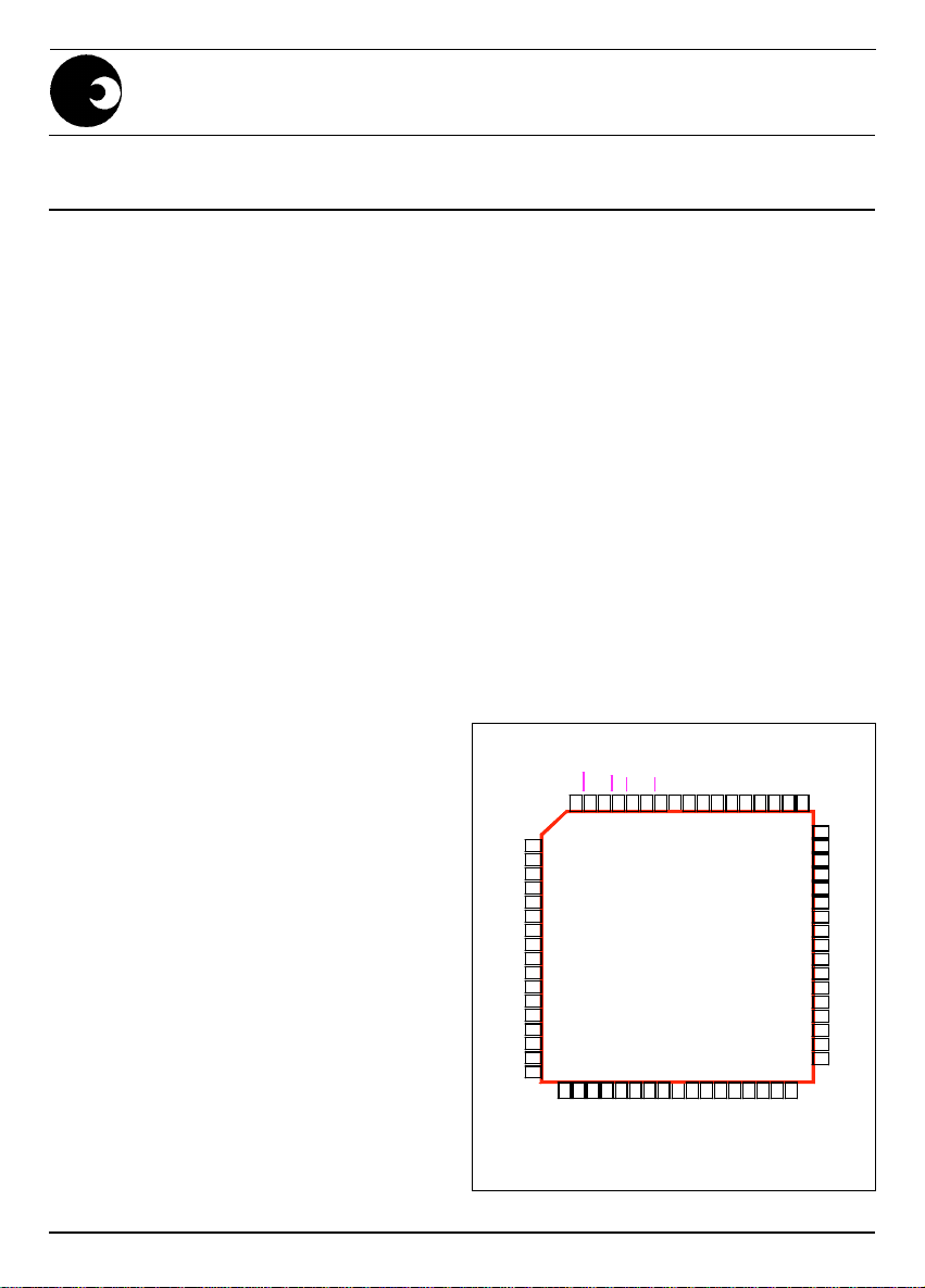
FIGURE 1: PIN CONNECTION FOR
SA9203
SA9203
33 34
32
31
2
1 6665646768
35
36 37 38 39
63
6162
PF
60
PF
59
PF
58
PF
57
PF
56
PF
55
PF
54
PF
53
52
51
PE
50
PE
49
PE
48
PE
47
PE
46
PE
45
PE
44
41
40
42
43
PA
10
0
PA
1
11
PA
12
2
PA
3
13
PA
4
14
PA
5
15
PA
6
16
PA
7
17
V
DD
18
PB
19
0
PB
20
1
PB
21
2
PB
22
3
PB
23
4
PB
5
24
PB
25
6
PB
26
7
DR-01266
9
876 543
28
27
29 30
4491
PDS039-SA9203/5-001 REV. A 20-08-96
1/14
Page 2
SA9203/5
Inter
face
AD(7:0
CON
PRTB
CON
PRTA
INT
RST
WR
ALE
CSRDSTBPPOR
F
POR
D
POR
E
PE(7:
PF(7:
PD(7:
POR
A
POR
C
POR
B
PC(7:
PA(7:
PB(7:
2
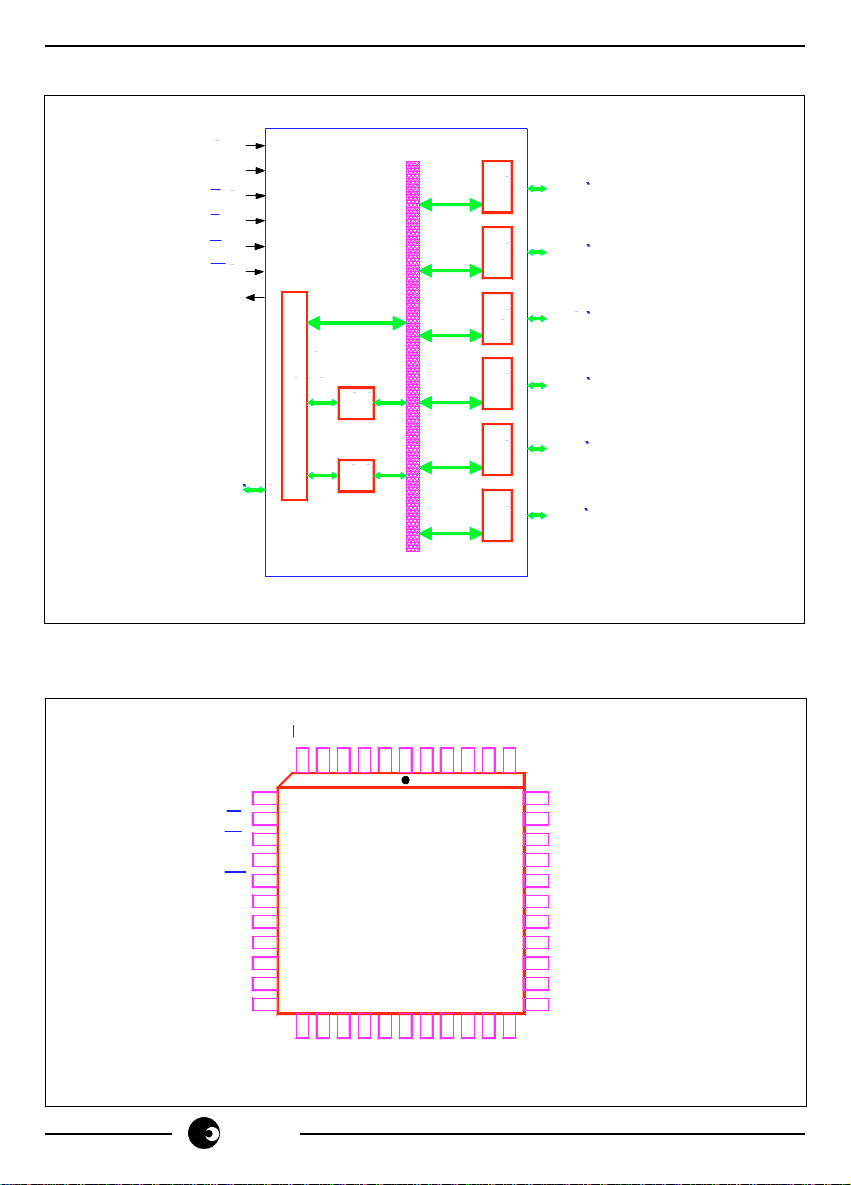
FIGURE 2: BLOCK DIAGRAM FOR SA9203
µµ
DR-01267
FIGURE 3: PIN CONNECTION FOR SA9205
CS
NC
AD
6
543
7
ALE
RD
8
WR
9
INT
10
RST
11
V
12
DD
STB
13
PA
14
0
PA
15
1
PA
16
2
PA
17
3
20 2119
18
4
5
6
PA
PA
PA
DR-01268
2/14
sames
7
5
6
AD
AD
SA9205
22
7
0
PA
PB
3
AD
26 27 28
2
PB
AD
3
PB
1
2
AD
4
PB
4
SS
AD
14344V42 41 40
23 2524
1
SS
V
PB
0
AD
5
PB
PC
39
7
PC
38
6
PC
37
5
PC
36
4
PC
35
3
V
34
DD
PC
33
2
PC
32
1
PC
31
0
PB
7
30
PB
29
6
Page 3

FIGURE 4: BLOCK DIAGRAM FOR SA9205
STB
ALE
CS
RD
WR
RST
INT
µµ
P
Inter-
face
AD(7:0)
DR-01269
CON
PRTA
CON.
PRTBC
PORT
A
PORT
B
PORT
C
SA9203/5
PA(7:0)
PB(7:0)
PC(7:0)
ABSOLUTE MAXIMUM RATINGS*
(All voltages are with respect to VSS)
Parameter Symbol Min Max Unit
Supply Voltage VDD-V
Voltage on any pin V
Current at any pin I
Storage Temperature T
M
STG
Operating Temperature T
SS
M
O
V
SS
7,0 V
VSS-0.3 VDD+0.3 V
100 mA
-40 +125 °C
0 +70 °C
* Stresses above those listed under “Absolute Maximum Ratings” may cause permanent
damage to the device. This is a stress rating only. Functional operation of the device
at these or any other condition above those indicated in the operational sections of this
specification, is not implied. Exposure to Absolute Maximum Ratings for extended
periods may affect device reliability.
sames
3/14
Page 4
SA9203/5
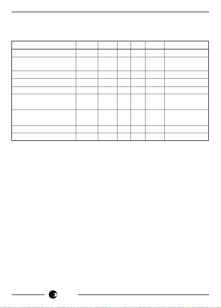
ELECTRICAL CHARACTERISTICS
(All measurements with respect to VSS, at 25°C, unless otherwise specified)
Parameters Symbol Min Typ Max Unit Condition
Supply Voltage V
Static Current I
DDS
4.75 5.0 5.25 V
DD
15 50 µA VDD = 5.0V
(See Note1)
Dynamic Current I
Input High Voltage V
Input Low Voltage V
Output High Voltage V
Output Low Voltage V
Input Leakage Current I
Tristate Leakage Current I
DDD
OH
OL
IN
TL
IH
IL
2.0 V VDD = 5.0V
4.5 4.7 V VDD = 5.0V
20 mA VDD = 5.0V
1.0 V VDD = 5.0V
I
= 5mA
OH
0.25 0.5 V VDD = 5.0V
I
= 5mA
OH
<1.0 3.0 µA VDD = 5.0V
<1.0 3.0 µA VDD = 5.0V
Note 1: All inputs tied to VDD or VSS with outputs not loaded.
Measurements made after RST applied.
4/14
sames
Page 5
SA9203/5
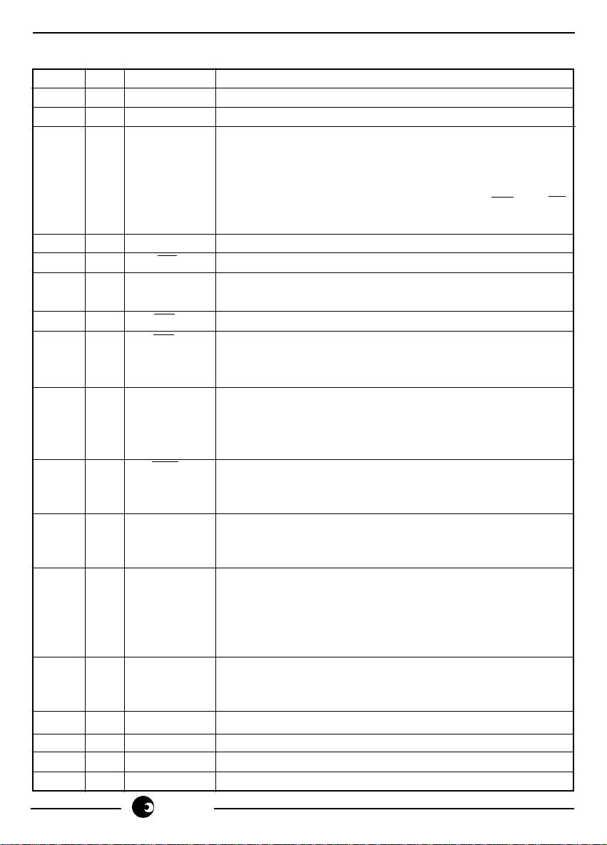
PIN DESCRIPTION for SA9203
Pin Type Designation Description
18,52 VDD +5V Supply Input
1,35 VSS 0V ground Reference
61..68 I/O AD0..AD7 3-state address/data lines that interface with the CPU
lower 8-bit address/data bus. The 8-bit address is
latched into the SA9203 internal address latch on the
falling edge of ALE. The 8-bit data is respectively
written into and read out of the SA9203 on WR and RD
signals.
2 N/C Not connected.
3 I CS Active low input signal used to select the device.
4 I ALE This control signal latches the address on the AD0..7
lines on the falling edge of ALE.
5 I RD Input low on this line enables the data bus buffers.
6 I WR Input low on this line causes the data on the address/
data bus to be written to the I/O ports and, control
registers.
7 O INT If enabled via A.6, this output will be set (active edge
polarity programmed by D6 and output polarity
programmed via D7 of the Port B-F direction control
register) after data has been latched into PORT A.
8 I RST Input low on this line resets the chip and all internal
registers and all ports to input mode (The register
contents after a reset pulse will be described later).
9 I STB Input data on PORT A pins will be latched when STB is
active and transparent otherwise (polarity programmed
by D5 of the Port B-F direction control register)
10..17 I/O PA0..PA7 8 general purpose I/O pins comprising PORT A. This
port supports individual input or latched output
configuration of each pin. In addition,each pin of PORT
A selected as an input can be programmed to be
latched or transparent.
19..26 I/O PB0..PB7 8 general purpose I/O pins comprising PORT B. All 8
pins are programmed to be either latched outputs or
transparent inputs.
27..34 I/O PC0..PC7 Identical to PORT B
36..43 I/O PD0..PD7 Identical to PORT B
44..51 I/O PE0..PE7 Identical to PORT B
53..60 I/O PF0..PF7 Identical to PORT B
sames
5/14
Page 6
SA9203/5
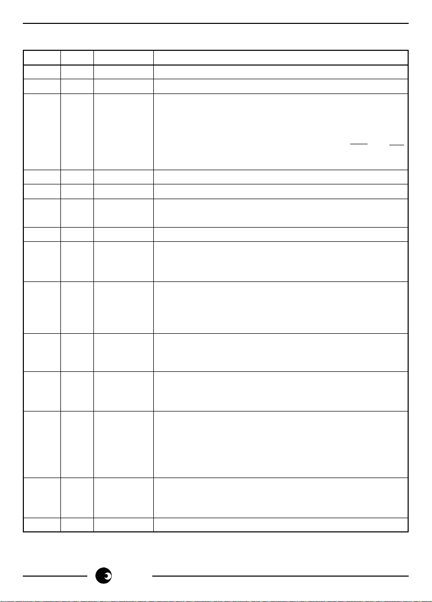
PIN DESCRIPTION for SA9205
Pin Type Designation Description
2,35 VDD +5V Supply Input
1,23 VSS 0V ground Reference
40..44 I/O AD0..AD7 3-state address/data lines that interface with the CPU
lower 8-bit address/data bus. The 8-bit address is
latched into the SA9203 internal address latch on the
falling edge of ALE. The 8-bit data is respectively
written into and read out of the SA9203 on WR and RD
signals.
5 N/C Not connected.
6 I CS Active low input signal used to select the device.
7 I ALE This control signal latches the address on the AD0..7
lines on the falling edge of ALE.
8 I RD Input low on this line enables the data bus buffers.
9 I WR Input low on this line causes the data on the address/
data bus to be written to the I/O ports and, control
registers.
10 O INT If enabled via A.6, this output will be set (active edge
polarity programmed by D6 and output polarity
programmed via D7 of the Port B-F direction control
register) after data has been latched into PORT A.
11 I RST Input low on this line resets the chip and all internal
registers and all ports to input mode (The register
contents after a reset pulse will be described later).
13 I STB Input data on PORT A pins will be latched when STB is
active and transparent otherwise (polarity programmed
by D5 of the Port B-F direction control register)
14..21 I/O PA0..PA7 8 general purpose I/O pins comprising PORT A. This
port supports individual input or latched output
configuration of each pin . In addition,each pin of
PORT A selected as an input can be programmed to be
latched or transparent.
22, I/O PB0..PB7 8 general purpose I/O pins comprising PORT B. All 8
24.30 pins are programmed to be either latched outputs or
transparent inputs.
31..39 I/O PC0..PC7 Identical to PORT B
6/14
sames
Page 7
SA9203/5
FUNCTIONAL DESCRIPTION
The SA9203 contains the following:
• Six 8-bit general purpose I/O ports programmable to be either byte or bit addressable.
• Two control registers for configuring the device. These control registers can be read
back.
• An internal address latch for accessing a multiplexed CPU address/data bus.
• The SA9203 appears to the CPU as a peripheral device occupying 256 bytes of
memory space. Certain locations in the memory map are occupied by the six I/O
ports and two control registers.
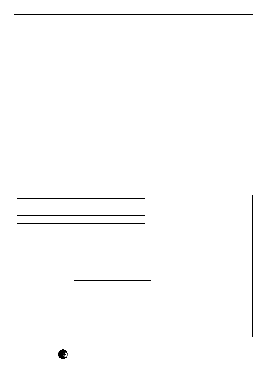
The SA9203 supports two basic I/O port addressing modes, via; byte-addressing and
bit-addressing. Any of the six I/O ports can be configured as byte-addressable /or bitaddressable. In bit-addressing, individual bits of any I/O port can be addressed
independently. In a bit- addressing CPU read operation, D0 contains valid data while
D1..D7 should be ignored. In a bit-addressing CPU write operation, D0 will be written
to the addressed output pin while D1..D7 will be ignored. The Address Memory map
is shown in Figure 5. The bit-addressing mode applies to both the I/O ports and the
control registers. The SA9205 is a three port device with operation is identical to the
SA9203.
FIGURE 5: Address Memory Map
WWWWWWWW
A7 A6 A5 A4 A3 A2 A1 A0
BM EI CR2 CR1 CR0 BM2 MB1 BM0
sames
Bit mode address 0
Bit mode address 1
Bit mode address 2
Control register address 0
Control register address 1
Control register address 2
0: Interupt function disabled
1: Interupt function enabled
0: Bit mode addressing enabled
1: Byte mode addressing enabled
7/14
Page 8
SA9203/5
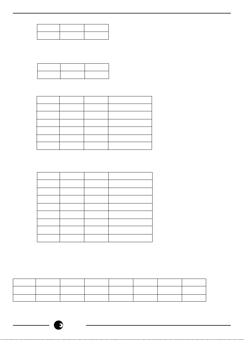
FIGURE 6: PORT A Direction Control Register Address.
A5 A4 A3
110
FIGURE 7: PORT B..F Direction Control Register / Strobe Control Register
Address
A5 A4 A3
11 1
FIGURE 8: PORT Addresses
A5 A4 A3 PORT
0 0 0 PORT A
0 0 1 PORT B
0 1 0 PORT C
0 1 1 PORT D *
1 0 0 PORT E *
1 0 1 PORT F *
* - n/a for the SA9205
FIGURE 9: Port Pin Addresses (Bit Mode Only).
A2 A1 A0 PORT PIN
0 0 0 PORT A-F.0
0 0 1 PORT A-F.1
0 1 0 PORT A-F.2
0 1 1 PORT A-F.3
1 0 0 PORT A-F.4
1 0 1 PORT A-F.5
1 1 0 PORT A-F.6
1 1 1 PORT A-F.7
Note : PORT A-C for SA9205
CONTROL REGISTERS
FIGURE 10: PORT A Direction Control Register
R/W R/W R/W R/W R/W R/W R/W R/W
D7 D6 D5 D4 D3 D2 D1 D0
PA.7 PA.6 PA.5 PA.4 PA.3 PA.2 PA.1 PA.0
D = 1 Port A Pin configured as output
D = 0 Port A Pin configured as input.
8/14
sames
Page 9
SA9203/5
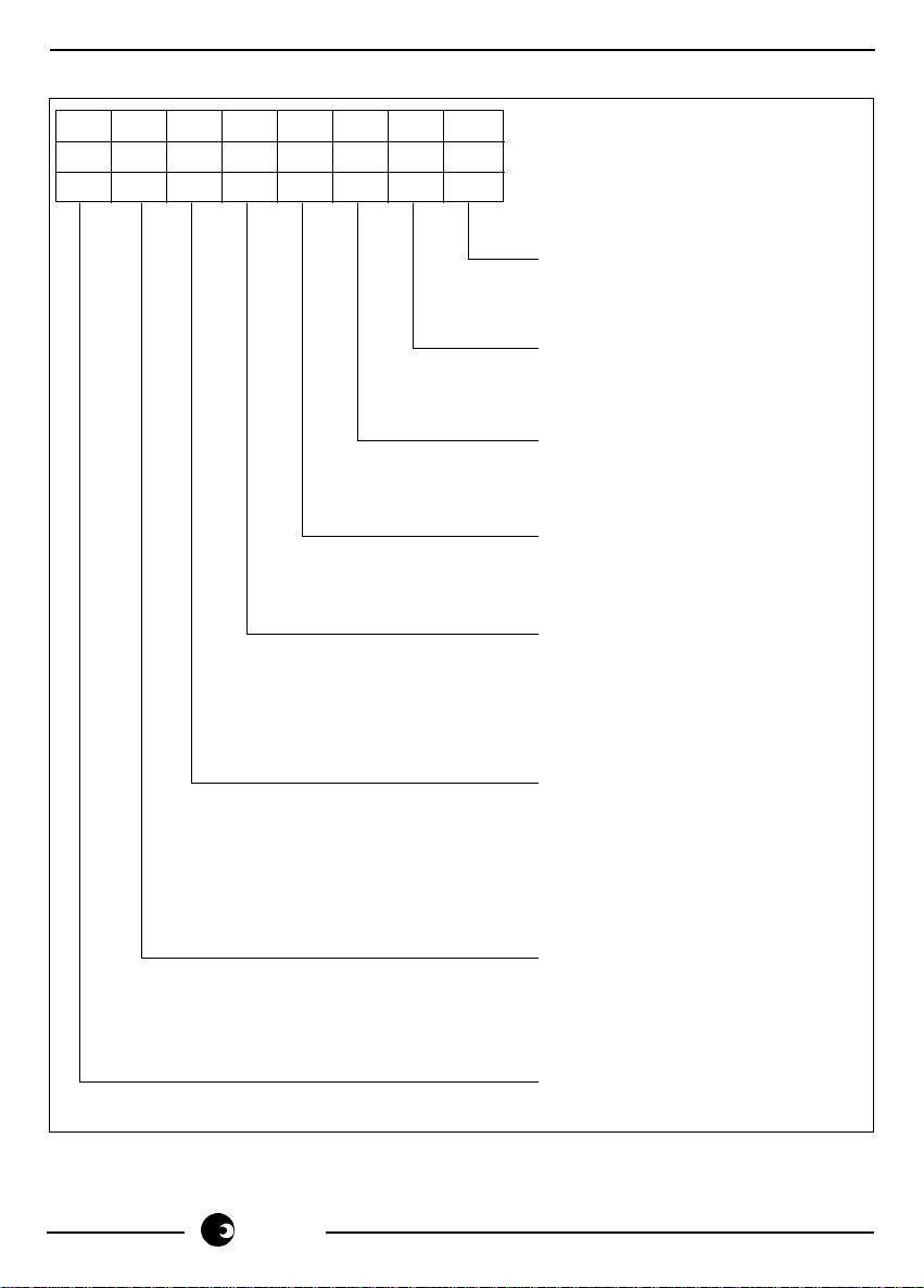
FIGURE 11: PORT B-F Direction Control / Strobe Control Register Address
R/W R/W R/W R/W R/W R/W R/W R/W
D7 D6 D5 D4 D3 D2 D1 D0
IP IE SP DF* DE* DD* DC DB
0: PORT B Configured as input
1: PORT B Configured as output
0: PORT C Configured as input
1: PORT C Configured as output
0: PORT D Configured as input
1: PORT D Configured as output
0: PORT E Configured as input
1: PORT E Configured as output
0: PORT F Configured as input
1: PORT F Configured as output
* n/a for the SA9205
sames
0: PORT A data latched when
STB low and transparent when
STB high.
1 - Port A data latched when
STB high and transparent when
STB low.
0 - Interupt output (INT) set on
the rising edge of STB.
1 - Interupt output (INT) set on
the falling edge of STB.
0: Interupt output active High
1: Interupt output active low
9/14
Page 10
SA9203/5
INT
This active high output (default after reset) operates as follows:
When disabled (via A6), INT remains reset. On either the rising or trailing edge of STB
(programmable via D6 of Port B-F direction control register), INT is set. INT remains
set until Port A (or any bit of PORT A if in bit- addressing mode) is read by the
microprocessor at which point INT is reset, remaining so until the next active edge of
STB. (See figure 14 for timing diagram). The output polarity of INT is programmed via
D7 of the Port B- F dirction control register (See Figure 11).
RST
This active low reset signal resets the contents of all registers to zero. Sets all ports to
input mode and the bi-directional data/address bus to input. A valid RST signal is
specified as an active low pulse of 100ns minimum duration.
CS
The active low CS signal is internally latched by the trailing edge of ALE.
TIMING DIAGRAMS
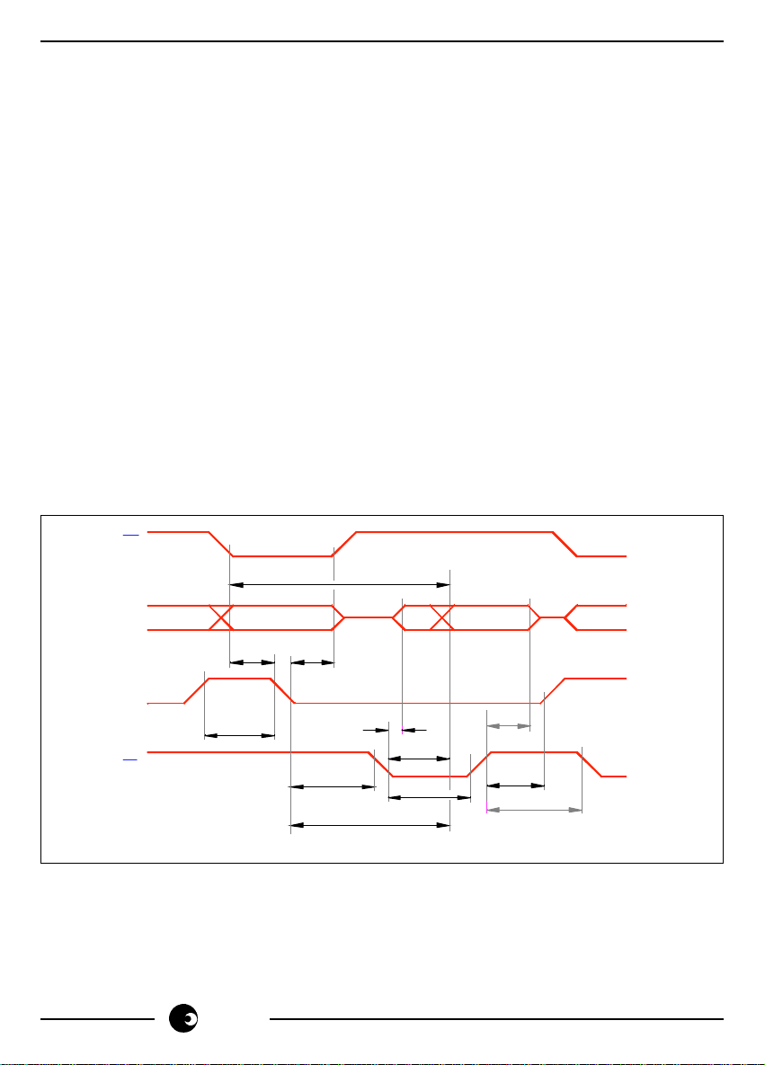
FIGURE 12: µP Read Waveforms
CS
t
AD
10/14
AD -8/A
08
ALE
RD
DR-01270
t
t
LL
sames
ADDRESS
t
AL
LA
DATA VALID
t
RDE
t
RD
t
LC
t
LD
t
CC
t
RDF
t
CL
t
RV
Page 11
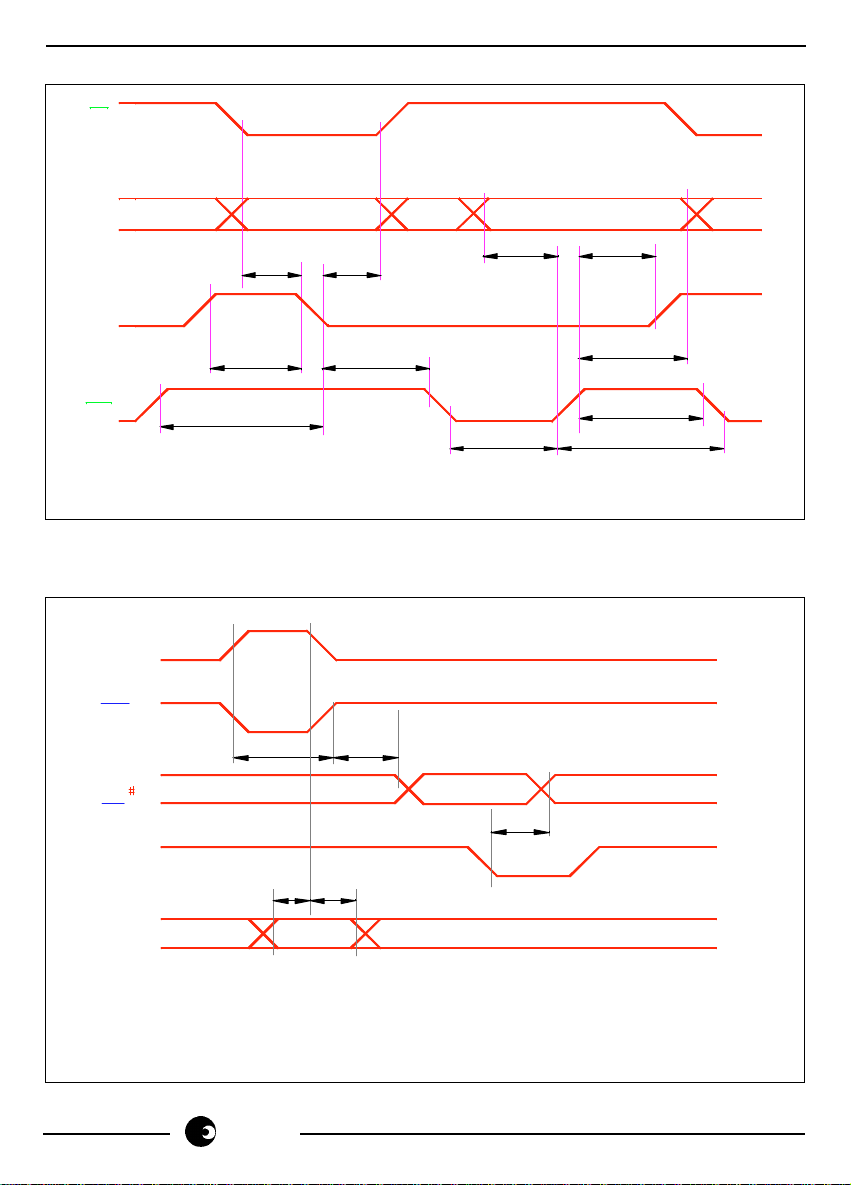
FIGURE 13: µP Write Waveforms
CS
SA9203/5
AD -8/A
0
8
ADDRESS
t
AL
t
LA
ALE
t
LC
WR
DR-01271
t
CLL
t
LL
FIGURE 14: µP Strobe/Interrupt Waveforms
STB
OR*
STB
INT
or
INT
t
SS
t
SI
DATA VALID
t
DW
t
CC
t
RDI
t
CL
t
WD
t
t
RV
WT
t
PSS
INPUT
DATA
FROM
PORTA
* DEPENDENT ON SP
# DEPENDENT ON IP
DR-01272
sames
t
PHS
11/14
Page 12
SA9203/5
DR 01273
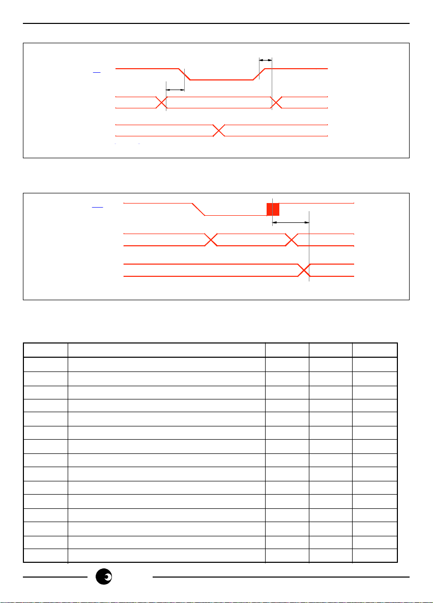
FIGURE 15: I/O Port Waveforms Transparent Output
t
RP
RD
INPUT
DATA BUS *
t
PR
X
DATA VALID
FIGURE 16: µP Read Waveforms Latched Output
WR
DATA BUS *
OUTPUT
DR-01274
X
DATA VALID
t
WP
X
Table 1: AC Characteristics for µP Interface1 - TA = 0°C to 70°C, VDD = 5V 10%
Symbol Parameter Min Max Units
t
t
t
t
t
12/14
t
AL
t
LA
t
LC
t
RD
t
LD
t
AD
t
LL
RDF
t
CL
CLL
t
CC
DW
WD
t
RV
RDE
Address to Latch Setup Time 10 ns
Address Hold Time after Latch 10 ns
Latch to READ/WRITE Control 10 ns
Valid Data Out Delay from READ Control 50 ns
Latch to Data Out Valid 50 ns
Address Stable to Data Out Valid 100 ns
Latch Enable Width 30 ns
Data Bus Float after READ 0 40 ns
READ/WRITE Control to Latch Enable 10 ns
WRITE Control to Latch Enable 50 ns
READ/WRITE Control Width 60 ns
Data in to WRITE Setup Time 20 ns
Data in Hold Time after WRITE 20 ns
Recovery Time between READ/WRITE 50 ns
Data Bus Enable from READ Control 10 ns
sames
Page 13
SA9203/5
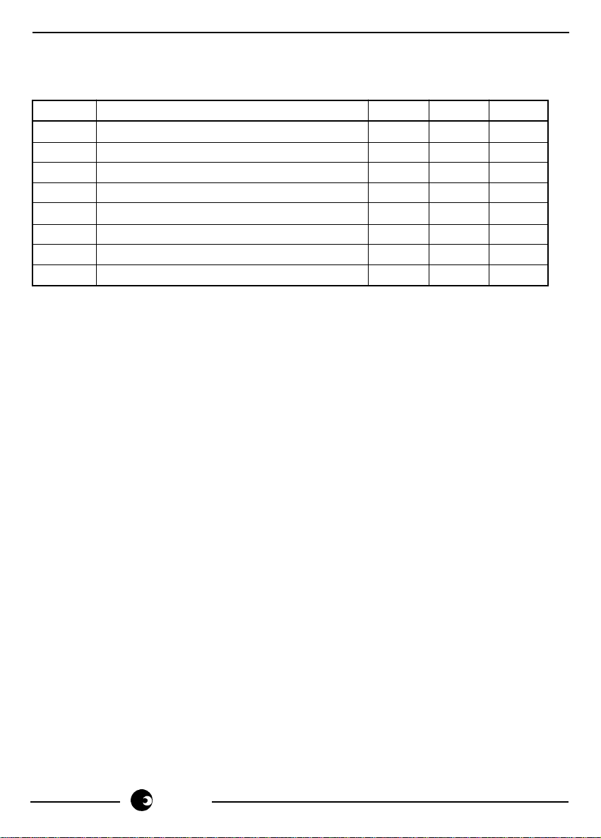
Table 2: A.C. Characteristics for I/O Ports
Symbol Parameter Min Max Units
t
t
t
t
t
t
t
PR
RP
SS
t
SI
RD
PSS
PHS
WP
Port Input Setup Time 20 ns
Port Input Hold Time 0 ns
Strobe Width 100 ns
Strobe to INT Set 100 ns
READ to INT Reset 100 ns
Port Setup Time to Strobe 50 ns
Port Hold Time After Strobe 120 ns
WRITE to Port Output 80 ns
Note 1: Timing parameters are preliminary and subject to change.
sames
13/14
Page 14

SA9203/5
Disclaimer: The information contained in this document is confidential and proprietary to South African Micro-
Electronic Systems (Pty) Ltd ("SAMES) and may not be copied or disclosed to a third party, in whole or in part,
without the express written consent of SAMES. The information contained herein is current as of the date of
publication; however, delivery of this document shall not under any circumstances create any implication that the
information contained herein is correct as of any time subsequent to such date. SAMES does not undertake to
inform any recipient of this document of any changes in the information contained herein, and SAMES expressly
reserves the right to make changes in such information, without notification,even if such changes would render
information contained herein inaccurate or incomplete. SAMES makes no representation or warranty that any
circuit designed by reference to the information contained herein, will function without errors and as intended by
the designer.
South African Micro-Electronic Systems (Pty) Ltd
P O Box 15888, 33 Eland Street,
Lynn East, Koedoespoort Industrial Area,
0039 Pretoria,
Republic of South Africa, Republic of South Africa
Tel: 012 333-6021 Tel: Int +27 12 333-6021
Fax: 012 333-8071 Fax: Int +27 12 333-8071
14/14
sames
 Loading...