

Page 1
sames
BLOCK MODE TIME SLOT ALLOCATION CIRCUIT
SA8702
SA8702
DESCRIPTION
The SA8702 (BMTSAC) is a Block Mode
Time Slot Allocation Circuit. The device is
used to generate 8 consecutive timeslots
in one of 4 blocks in a 32 time-slot PCM
system. Each timeslot pulse is 8 BLCK
cycles long. BCLK is the 2,048 station
clock provided by the system. An active
MRST will disable all outputs until a valid
XSYNC input is recognised. The output
TSX is delayed by half a cycle and indicates
that one of 8 timeslots is currently active.
There are 4 possible modes of operation,
selectable by means of the BL0 and BL1
pins (See Table 1).
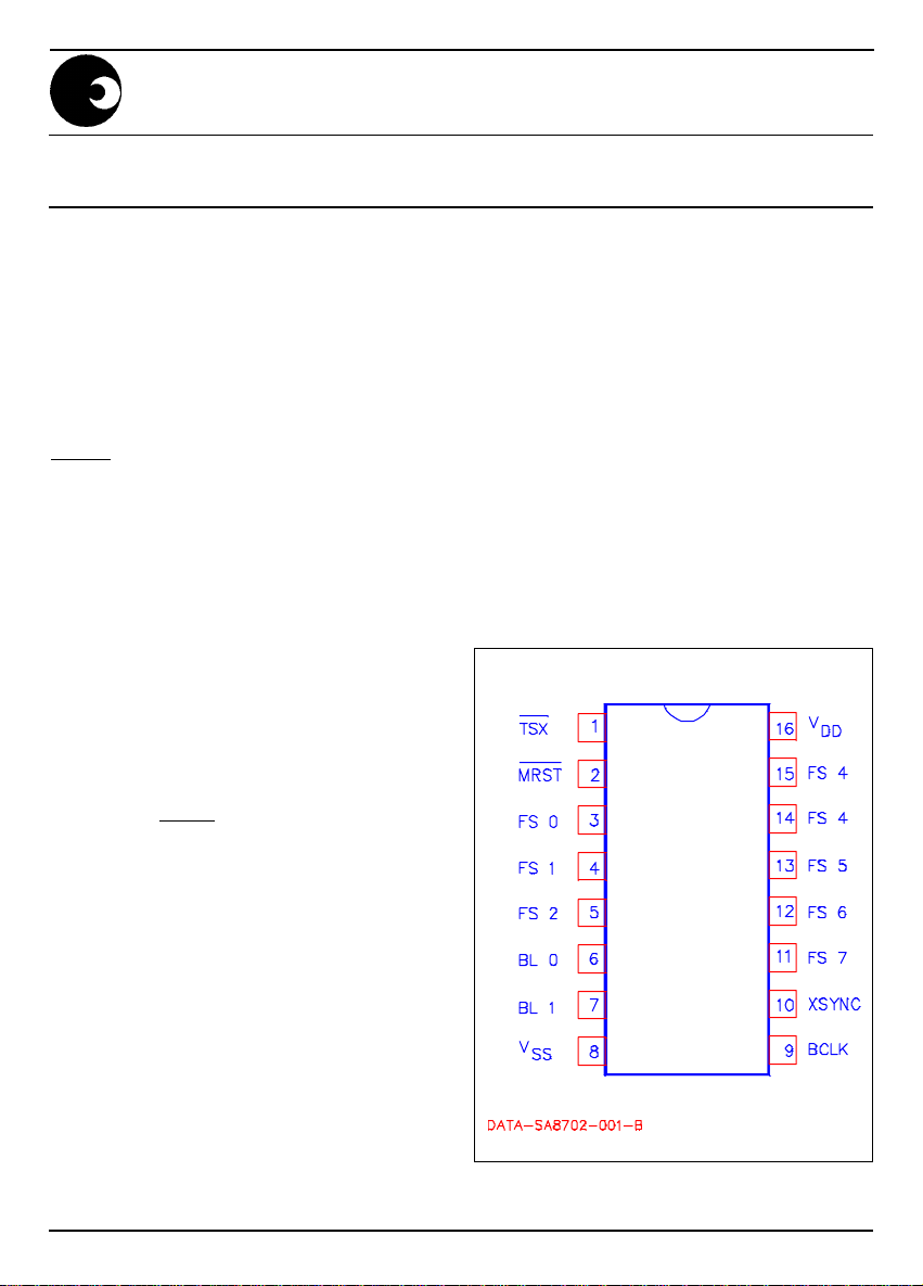
PIN CONNECTIONS
All inputs and outputs are C-MOS
compatible. All outputs are push-pull with
the exception of TSX which is open drain.
The inputs MRST and BCLK are Schmitt
Trigger. Inputs BL0 and BL1 have pull-ups.
(See figure 1).
APPLICATIONS
■ PCM Switching Systems
■ PCM Transmission Systems
■ Subscriber Multiplex Equipment
■ PBX Systems
SA8702
sames
Figure 1.
1
02.02.93
Page 2
SA8702
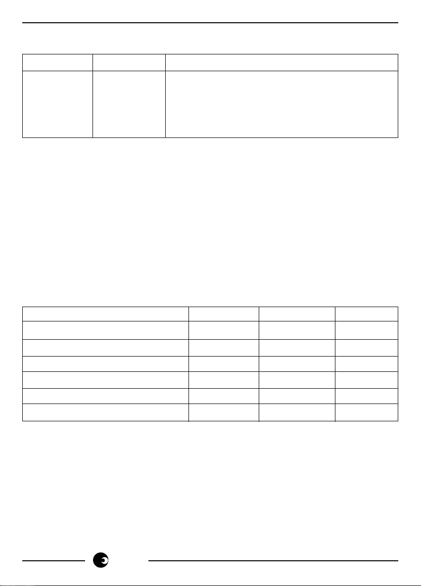
Operating Modes
BL1 BL0 Mode of Operation
0 0 Outputs active in timeslots 0 to 7
0 1 Outputs active in timeslots 8 to 15
1 0 Outputs active in timeslots 16 to 23
1 1 Outputs active in timeslots 24 to 31
Table 1.
Input pulse XSYNC occurs periodically in every frame and is used to generate the
first of the eight timeslots and also defines the beginning of Block 0. If XSYNC fails
high then the outputs will be generated as they were before the failure occured.
Should XSYNC fail low then the outputs will be deactivated after completion of the
frame.
Maximum Ratings
All voltages measured with respect to VSS.
Parameter Symbol Value Units
Supply voltage V
Positive voltage on any pin V
Negative voltage on any pin V
Maximum current through any pin I
Storage temperature T
Operating temperature T
Stresses beyond these values may cause permanent damage to the device. Exposure to
maximum rated conditions for extended periods may affect device reliability.
DD
HM
LM
HM
ST
O
+7,5 V
VDD +0,3 V
VSS -0,3 V
±10 mA
-55 to +150 °C
-10 to +70 °C
sames
2
Page 3
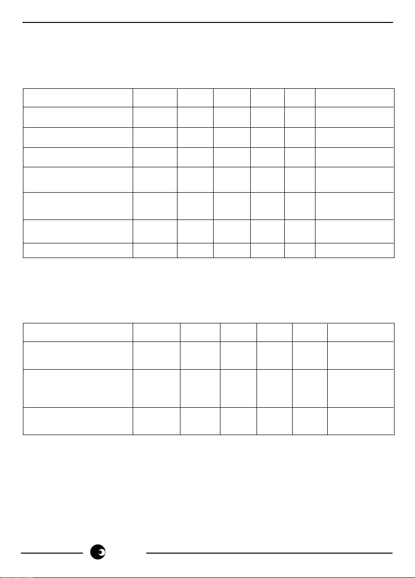
Operating Conditions:
All voltages measured with respect to VSS.
Inputs must never be left open.
DC Parameters Symbol Min. Nom. Max. Unit Conditions
SA8702
Supply Voltage V
* Input Low Voltage V
* Input High Voltage V
** Output Low Voltage V
** Output High Voltage V
DD
IL
IH
OL
OH
Operating Frequency - 2,048 2,273 MHz 4,75 ≤ V
4,75 5,00 5,25 V -
- - 1,0 V V
4,0 - - V V
- - 0,5 V V
4,5 - - V V
I
ol
I
oh
DD
DD
DD
DD
= 5V
= 5V
= 5V
= 0,5mA
= 5V
= 0,5mA
DD
≤ 5,25
Operating Temp. range -10 25 70 °C -
* All inputs are C-MOS level compatible. Pins 6 and 7 have internal pull-up
devices.
** All outputs are push-pull except pin 1 which is open drain.
AC Parameters Symbol Min. Nom. Max. Unit Conditions
XSYNC setup before T
s
60 - - ns 4,75 ≤ V
BCLK goes low ≤ 5,25
Output propagation T
pd
- - 150 ns 4,75 ≤ Vdd
delay from active clock ≤ 5,25
edge
XSYNC hold time from T
h
50 - - ns 4,75 ≤ V
BCLK ≤ 5,25
DD
DD
sames
3
Page 4
SA8702
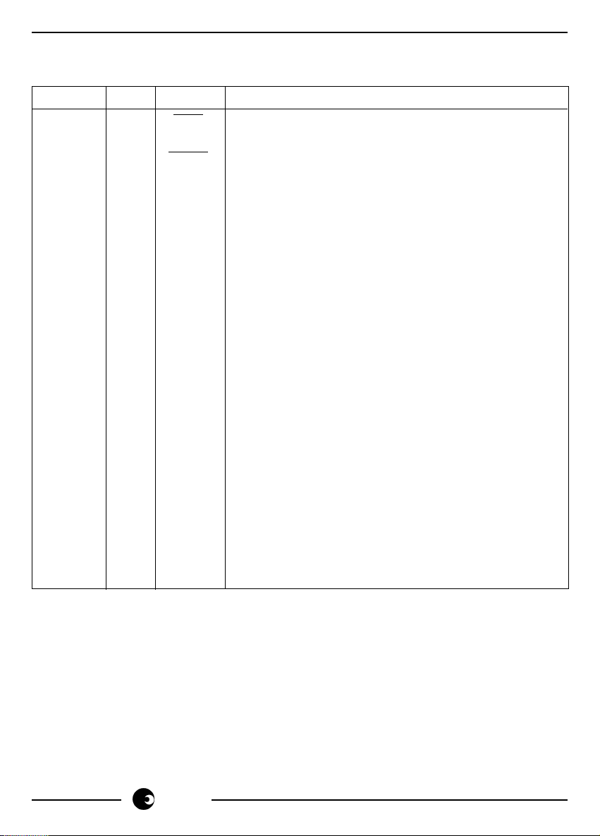
PIN DESCRIPTION
Pin No. I/O Name Description
1 O TSX An open drain N-channel high impedance, but pulls
low during any active timeslot.
2 I MRST A Schmitt trigger input that asynchronously disables
all outputs.
3 O FSO A timeslot output which is normally low, and goes
active-high for 8 cycles of BCLK when a valid XSYNC
is made.
4 O FS1 Similar to pin 3.
5 O FS2 Similar to pin 3.
6 I BL0 The input for the LSB of the 2 bit word which defines
the active block.
7 I BL1 The input for the MSB of the 2 bit word which defines
the active block.
8 I VSS The OV ground connection to the device.
9 I BCLK The 2,048MHz station clock input.
10 I XSYNC The input pulse XSYNC used to generate the first of
the eight timeslots and also defines the beginning of
block 0.
11 O FS7 Similar to pin 3.
12 O FS6 Similar to pin 3.
13 O FS5 Similar to pin 3.
14 O FS4 Similar to pin 3.
15 O FS3 Similar to pin 3.
16 I VDD The positive supply to the device.
sames
4
Page 5
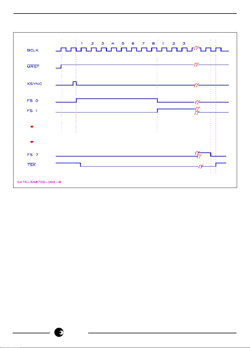
TIMING DIAGRAM
SA8702
sames
5
Page 6

SA8702
Disclaimer: The information contained in this document is confidential and proprietary to South African Micro-
Electronic Systems (Pty) Ltd ("SAMES") and may not be copied or disclosed to a third party, in whole or in part,
without the express written consent of SAMES. The information contained herein is current as of the date of
publication; however, delivery of this document shall not under any circumstances create any implication that the
information contained herein is correct as of any time subsequent to such date. SAMES does not undertake to
inform any recipient of this document of any changes in the information contained herein, and SAMES expressly
reserves the right to make changes in such information, without notification,even if such changes would render
information contained herein inaccurate or incomplete. SAMES makes no representation or warranty that any
circuit designed by reference to the information contained herein, will function without errors and as intended by
the designer.
Any sales or technical questions may be posted to our e-mail adress below:
[email protected]
For the latest updates on datasheets, please visit our web site:
http://www.sames.co.za
South African Micro-Electronic Systems (Pty) Ltd
P O Box 15888, 33 Eland Street,
Lynn East, Koedoespoort Industrial Area,
0039 Pretoria,
Republic of South Africa, Republic of South Africa
Tel: 012 333-6021 Tel: Int +27 12 333-6021
Fax: 012 333-8071 Fax: Int +27 12 333-8071
sames
6
 Loading...