

Page 1

sames
FEATURES
n Frame alignment/synthesis for PCM30
double frame and CRC-multiframe
format.
n Meets CCITT Rec.G704
n Interface to route selectable between
HDB3 and fibre optical
n HDB3 outputs switchable between fully
bauded and half bauded format
n Error checking via CRC4 procedure
n Insertion and extraction of alarms and
facility signals
n Selectable system - clock (4096 kHz/
8192 kHz)
n Selectable Interface mode (2048/4096
kBit/s) to system internal highway
n Programmable offsets for receive and
transmit data
n Two frame receive buffer for receive
route clock wander and jitter
compensation
n Slip detection and direction indication
n Extended HDB3 error detection
SA9101
PCM FRAME ALIGNER
n Error counters for code errors
(switchable to "Si zeros counter"), frame
errors and CRC4 errors
n Sub-multiframe assigned CRC Error
indication with possibility of automatic
insertion in Si-bit position of outgoing
multiframe.
n Simplified data transfer between
SA9101 and controller, supported by
data stacks for receive and transmit
signalling data, selectable interruptsources and DMA facilities.
n Double frame marker for serial data
extraction support
n Repeated transmission of signalling
data, if not updated.
n Three transparent modes for timeslot 0
in transmit direction
n Transparent mode for receive direction
n HDB3 error indication
n Idle channel data insertion selectable
for any timeslot
n Channel loopback capabilities, test and
diagnostic capabilities
n Parity checks
DESCRIPTION:
The SA9101 (Frame Alignment unit for PCM30 Systems) is a C-MOS device which
implements the interface to PCM30 Transmission Systems.
In the receive direction, the device performs HDB3 decoding, Frame alignment
(selectable between doubleframe and CRC-Multiframe) and extraction of signalling
data.
Wander absorption between the PCM carrier and the system internal highway is
performed using an internal 2 frame memory. The incoming data stream is monitored
and
M71-1797 PDS039-SA9101-001 REV.A 09-09-94
1/40
Page 2
SA9101
Description (Cont.)
status and error conditions are reported through the µP interface. In the transmit
direction, Frame (and Multiframe) alignment, signalling data insertion and HDB3 coding
is performed.
If Multiframe format is enabled, CRC4 extraction and checking are carried out in the
receive direction and CRC4 data is inserted in the transmit direction.
Stacks for transmit and receive signalling data with DMA capability as well as maskable
interrupt sources simplify interfacing to microcontrollers.
Alarm simulation capabilities and selectable channel-loopback, support system
diagnostics.
Different transparent modes for timeslot 0 in transmit direction simplify system test and
data transmission through the system.
Advanced algorithms for synchronisation of doubleframe and CRC4 multiframe format
data, and monitoring of frame and doubleframe formats minimise loss of data.
Control Registers allow different control settings through the µP interface.
Advanced C-MOS Technology ensures low power consumption and high reliability.
The device is upwards compatible with the Siemens ACFA (PEB 2035 V4.1) in PCM30
mode.
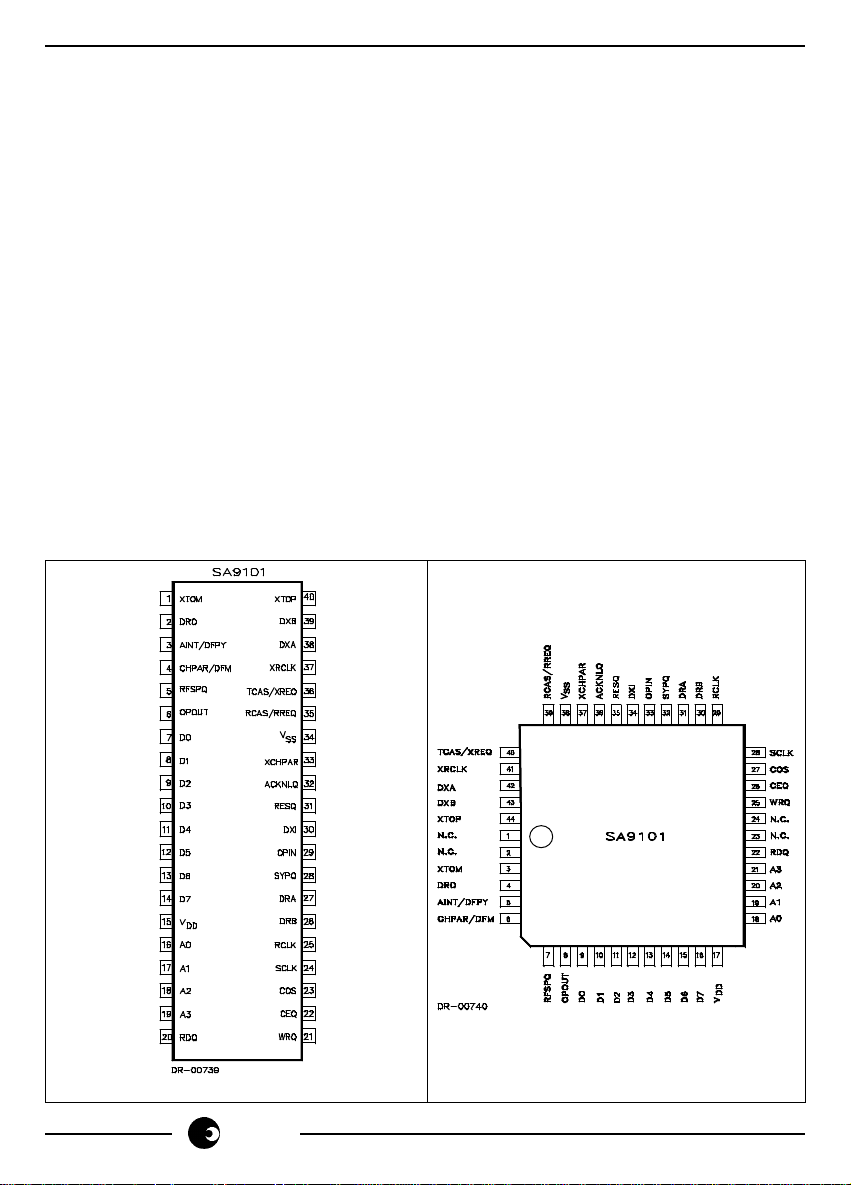
PIN CONNECTIONS
2/40
Package: DIP/DIC - 40 Package: PLCC - 44
sames
Page 3
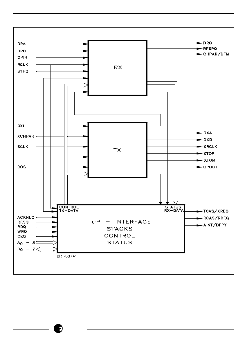
Block Diagram
SA9101
sames
3/40
Page 4

SA9101
ELECTRICAL CHARACTERISTICS
Absolute Maximum Ratings*
Parameters Symbol Min Max Unit
Supply Voltage V
Voltage on any I/O pin V
Current on any I/O pin I
Storage Temperature T
Operating Temperature T
Package Power Dissipation P
*Stress above those listed under "Absolute Maximum Ratings" may cause permanent damage
to the device. This a stress rating only. Functional operation of the device at these or any other
condition above those indicated in the operational sections of this specification, is not implied.
Exposure to Absolute Maximum Ratings for extended periods may affect device reliability.
DC Operational Characteristics
= 5V, T = 10°C..+70°C
V
DD
Parameter Symbol Min. Max. Unit Remarks
Supply Voltage V
Supply Current (dynamic) I
Standby Current I
Inputs
High Voltage V
Low Voltage V
Leakage Current I
Input ACKNQ
Pullup Current -I
Outputs
High Voltage V
Low Voltage V
Bidirects
Input High Voltage V
Input Low Voltage V
Tristate Current I
Output High Voltage V
Output Low Voltage V
Operational Characteristics
= 25°C; V
T
A
= 5V ±5%; VSS = 0V
DD
Parameter Symbol Min. Max. Unit
Input capacitance C
Output capacitance C
I/O C
4/40
sames
DD
- V
I/VO
I/IO
STG
OP
D
SS
-0.3 6 V
-0.3 VDD+0.3 V
Limit Values
DD-VSS
DD
DDS
LEAK
PUP
OH
OL
LEAK
OH
OL
4.5 5.5 V
2.4 V
IH
IL
-5 5 µA VI=0..V
10 30 µA VI=0
2.8 V IOH=-1mA
2.4 V
IH
IL
-10 10 µA VI=0..V
2.8 V IOH=-1mA
Limit Values
IN
OUT
IO
20 mA
-55 +125 °C
-10 +70 °C
1000 mW
100 mA
100 µA
0.8 V
DD
0.4 V IOL=2mA
0.8 V
DD
0.4 V IOL=2mA
10 pF
15 pF
20 pF
Page 5

PIN DESCRIPTION
SA9101
Pin Name Direction Description
Pin No.
DIL PLCC
AINT/DFPY O 3 5 Alarm interrupt/Double Frame Parity
ACKNLQ I 32 36 DMA Acknowledge
A[3-0] I 19-16 21-18 Address Bus
CEQ I 22 26 Chip Enable
CHPAR/DFM O 4 6 Receive Channel Parity/
Double Frame Marker
COS I 23 27 Carrier out of Service
DRA I 27 31 Receive Data in Plus
DRB I 26 30 Receive Data in Minus
DRO O 2 4 Receive Data Out
DXA O 38 42 Transmit Data Out Plus
DXB O 39 43 Transmit Data Out Minus
DXI I 30 34 Transmit Data In
D[7-0] B 14-7 16-9 Data Bus
OPIN I 29 33 Receive Optical Interface Data
OPOUT O 6 8 Transmit Optical Interface Data
RCAS/RREQ O 35 39 Receive TS16 Signal/Receive DMA
Interrupt Request
RCLK I 25 29 Receive Route Clock
RDQ I 20 22 Read Enable
RESQ I 31 35 Reset
RFSPQ O 5 7 Receive Frame Synchronisation
Pulse
SCLK I 24 28 System Clock
SYPQ I 28 32 Synchronisation Pulse
TCAS/XREQ O 36 40 Transmit TS16 Signal/Transmit DMA
Interrupt Request
V
DD
V
SS
S 15 17 +5V Supply
S 34 38 0V Ground
WRQ I 21 25 Write Enable
XCHPAR O 33 37 Transmit Channel Parity
XRCLK O 37 41 Transmit Route Clock
XTOM O 1 3 Test Data Output Minus
XTOP O 40 44 Test Data Output Plus
sames
5/40
Page 6

SA9101
DESCRIPTION OF INTERFACES
Fibre Optical Interface
The fibre optical interface is enabled via the microprocessor interface.
Signal Pin Input/Output/Bidirect Function
OPIN 29 I Optical Fibre In
Unipolar Input Signal at 2048 kbps
Input polarity sense is programmable
via CR8B3. Latching of data is
performed with the falling edge of
RCLK if optical interface is selected
via CR1B2. (See Fig. 6 Line Interface
Timing.)
OPOUT 6 O Optical Fibre Out
Unipolar Output Signal at 2048 kbps
The output's active polarity is
programmable via CR6B7. Data is
clocked out on the rising edge of
XRCLK. Data duty cycle is 100%.
(See Fig. 6 Line Interface Timing.)
RCLK 25 I Route Clock
This clock, derived from the incoming
data by the line interface circuit (eg.
IPAT (PEB2235)), is necessary for
clocking received data into the SA9101.
XRCLK 37 O Transmit Route Clock
This 2048kHz clock is generated from
the Station Clock, SCLK. (See Fig. 5
System Interface Timing and Fig. 6
Line Interface Timing.)
PCM30 Interface
Signal P i n Input/Output/Bidirect Function
DRA 27, I Data Receive +/DRB 26 I HDB3 coded PCM Signal
DXA 38, O Data transmit +/DXB 39 O HDB3 coded PCM Signal
RCLK 25 I Route Clock f = 2.048 MHz
XRCLK 37 O Transmit route clock
6/40
sames
Page 7

SA9101
Clock Generator
Signal Pin Input/Output/Bidirect Function
SCLK 24 I System Clock f=4,096 MHz/8,192MHz
RFSPQ 5 O Receive Frame Pulse
Frequency: 8 kHz
Duration: 488 ns
If loss of synchronisation, the line frame
pulse is inhibited
SYPQ 28 I Synchronous Pulse
Defines start of frame for System internal
data, together with the programmed offset
values of transmit and receive counter.
Pulse width: >244 ns
Period: Multiples of 125µs
DIU Controller
Signal Pin Input/Output/Bidirect Function
D0 - D7 7 - 14 B Bidirectional 8 bit data-bus
A0 - A3 16 - 19 I Address lines for SA9101 internal
registers
CEQ 22 I Chip enable input
WR Q 21 I Write enable input
RDQ 20 I Read enable input
COS 23 I Carrier out of service input.
SA9101 sends AIS to PCM30 interface
if input is at “1”
XREQ 36 O Transmit DMA interrupt request
RREQ 37 O Receive DMA interrupt request
AINT 3 O Alarm interrupt request
ACKNLQ 32 I DMA Acknowledge (Active Low)
(Not used when CR6B6 = 0. If not used
then pin must be fixed to V
internal TS16 signalling stacks is enabled
this input acts as an "access enable" to the
internal stacks (CRAB0-7 for T
SR7B0-7 for R
read/write command without the need of
) in conjunction with a
X
generating the chip enable signal at CEQ.
In this case it is to be connected to the
acknowledge output of the DMA controller.
.) If access to
DD
and
X
sames
7/40
Page 8

SA9101
System Internal Highway
Signal Pin Input/Output/Bidirect Function
DRO 2 O Data Receive Out
DXI 30 I Data Transmit In
Timeslot channels 0 - 31 to/from PCM30 interface.
Bit rate 2048 kbit/s or 4096 kbit/s selectable via microprocessor interface.
CAS Processing
Signal Pin Input/Output/Bidirect Function
DRO 2 O Data Receive Out
DXI 30 I Data Transmit In
RCAS 35 O Receive CAS, active high marks
reception of channel 16
TCAS 36 O Transmit CAS, active high marks
transmission of channel 16
Test/Supervision
Signal Pin I nput/Output/Bidirect Function
CHPAR 4 O Receive Channel parity
Appears according to the related
channel (timeslot)
DFPAR 3 O Doubleframe Parity
During a current double-frame, the
parity of the previous double-frame
appears on DFPAR
XTOP 40, O HDB3-coded PCM (+), PCM (-) signal
XTOM 1 O for HDB3 diagnostic loop
RESQ 31 I Reset (Output Disable)
Asynchronous reset signal (active low),
resets the internal circuit and switches
all outputs to high impedance state -
must be held low for minimum of 2µs
XCHPAR 33 I Transmit channel parity
8/40
sames
Page 9

SA9101
FUNCTIONAL DESCRIPTION
Receive path
Receive Link Interface
For data input, two different data types, with selectable input active polarity sense, are
supported:
- Dual rail data (PCM[+], PCM[-]) at ports DRA, DRB received from a Line Interface
Unit.
- Unipolar data at port OPIN (PCM 30) received from a fibre optical Interface.
Latching of data is carried out using the falling edge of the Receive route Clock
(RCLK, 2048 kHz) recovered from the PCM receive data stream. Dual rail data is
subsequently converted into a single rail, unipolar bit stream. The HDB3 line code
is used along with Double Violation Detection or Extended Code Violation Detection
(selectable). These errors increment the Code Violation Counter.
When using the unipolar input mode, the decoder is by-passed and no code violation
will be detected.
Additionally, the receive Link Interface comprises the alarm detection for AIS (Alarm
Indication Signal: unframed bit stream with constant logical ‘one’) and NOS (No
Signal: Input signal with insufficient bit rate or insufficient density of ones).
The single rail bit stream is then processed by the Receiver.
Receiver
The following functions are performed:
- Synchronization of pulse frame
- Synchronization of CRC4 multi-frame
- Error Indication when pulse frame synchronization is lost. In this case, AIS is sent to
the system side. If the receiver is in transparent mode, AIS is suppressed.
- Initiating and controlling of re-synchronization after loss of synchronization. This may
be carried out automatically by the SA9101, or under user control via the microprocessor
interface.
- Detection of Remote Alarm Indication from the incoming data stream.
- Separation of service bits and data link bits. This information is stored in special status
registers.
- Generation of control signals to synchronize the CRC checker, the parity generator,
and the Receive Speech Memory control unit.
If the multi-frame format is selected, CRC checking of the Incoming data stream is
done by generating check bits for a CRC submultiframe according to the CRC 4
procedure (PCM30, refer to CCITT Rec. G704). These bits are compared with those
check bits that are received during the next CRC sub-multiframe. If there is a
mismatch, the CRC error counter will be incremented. This 8-bit counter (default) can
be extended to 10-bit length, by writing to the control registers.
sames
9/40
Page 10
SA9101
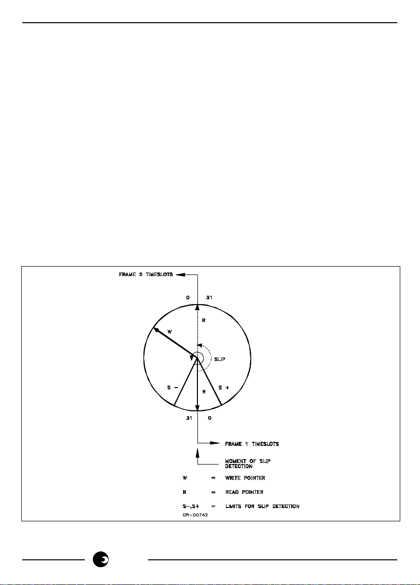
Receive Speech Memory
The speech memory is organized as a two-frame elastic buffer with a size of 64 x 9 bit
(8-bit channel data plus one parity bit).
The functions are:
- Compensation of Input wander and jitter. Maximum wander amplitude (peak-to-
peak) = 190 UI (1UI = 488 nS)
- Frame alignment between system frame and receive route frame
- Reporting and controlling of slips
Controlled by special signals generated by the Receiver, the unipolar bit stream is
converted into bit-parallel, channel-serial data which is circularly written to the speech
memory. At the same time, a parity signal is generated over each channel and also
stored in the speech memory.
Reading of stored data is controlled by the System Clock (SCLK) and the Synchronization
Pulse (SYPQ) in conjunction with the programmed offset values for the Receive timeslot/
Clock slot Counters. After conversion into a serial data stream and parity checking
(errors are reported via the status registers), the data is given out via port DRO. Channel
parity information is output at port CHPAR with selectable parity type (odd or even). Two
bit rates (2048/4096 kbps) are selectable via the microprocessor interface.
Figure 1.0: The Receive Speech Memory as circularly organized memory
10/40
sames
Page 11

SA9101
Figure 1.0 illustrates the operation of the receive Speech Memory:
A slip condition is detected when the Write Pointer (W) and the Read pointer (R) of the
memory are nearly coincident, i.e. the Write pointer is within the Slip Limits (S+, S-). If
a slip condition is detected, a negative slip ( the next received frame is skipped) or a
positive slip (the previous received frame is read out twice) is performed at the System
Interface, depending on the difference between RCLK and SCLK, i.e. on the position of
pointer R and W within the memory.
To reduce delay, the Receive Speech Memory can be switched to one frame length. For
correct operation, System Clock SCLK and Synchronization Pulse SYPQ have to be
derived from the Receive Route Clock RCLK and the Receive Frame Synchronous Pulse
RFSPQ (PLL application). In Single Frame Mode, however, it is not possible to perform
a slip after the slip condition has been detected.
Receive Transparent Mode
If enabled, the frame aligner does not try to synchronise on the received data if
synchronisation is lost. The AIS to the System Interface is disabled. The data appears
on the System Interface synchronised to the System Clock (SCLK) as received.
Transmit path
The PCM data is received from the system internal highway at port DXI at 2048 kbps or
4096 kbps. The channel assignment is equivalent to the receive direction. Data in invalid
timeslots will be ignored.
Latching of data is controlled by the System Clock (SCLK) and the Synchronization Pulse
(SYPQ), in conjunction with the programmed offset values of the Transmit Timeslot/
Clockslot Counters.
The Transmit Route Clock (XRCLK) is derived directly from the system clock by an
internal clock divider. Consequently, the data received from the system interface is
switched through without the need of intermediate storage.
The parity generation/checking mechanism is symmetrical to the receive path. The
channel data is checked with the channel parity information generated internally or
externally (input at port XCHPAR with selectable parity type). Errors are reported to the
microprocessor interface. To avoid difficulties with external parity generation, the parity
signal for non-speech data (TS0 and TS16) is ignored.
Transmitter
The serial bit stream is then processed by the transmitter which has the following
functions:
- Frame/multiframe synthesis of one of the selectable framing formats
- Insertion of service and data link information.
- Remote Alarm generation
- CRC generation and insertion of CRC bits
sames
11/40
Page 12

SA9101
Transmit Link Interface
Similar to the Receive Link Interface two different data types with selectable active
polarity for the output are supported:
- Dual rail data (PCM[+], PCM[-]) at ports DXA, DXB with selectable duty cycle (50%
or 100%) transmitted to a Line Interface Unit. Single rail data is converted into a dual
rail bit stream. The HDB3 line code is employed.
- Unipolar data at port OPOUT with 100% duty cycle transmitted to a fibre optical
interface.
Clocking of data is carried out on the positive transitions of the Transmit Route Clock:
XRCLK (2048 kHz). XRCLK is generated by the SA9101.
Additionally, the dual rail outputs XTOP and XTOM are provided for test applications.
Additional functions
Alarm Interrupt
Normally, the control of data transmission via the PCM line is carried out by polling the
internal status registers of the SA9101 at equal time intervals. However, for fast error
handling the option exists to configure a specific output port as interrupt port (AINT). This
signal may be connected to an interrupt input of the on-board processor. Triggering of
the output may be caused by up to 10 maskable interrupt sources.
Single Channel Loop Back
As one of the extended test options, the Single Channel Loop Back enables reflection
of a selected channel back to the system interface at port DRO.
TS16 Extraction/Insertion
TS16 data can be extracted/inserted via the µP or the DMA facility provided. For µP
interface, RREQ/XREQ act as interrupts. When one of these interrupts is received two
bytes must be read/written consecutively before next frame information is written into it.
For DMA operation see detailed timing diagram, Fig 7.3. (See DIU Controller Pin
description table, CR6B6 Register and SR5B5 Register descriptions.)
Data Extraction/Insertion is also possible through the serial ports DRO and DXI by using
a multiplexer in conjunction with the control signals RCAS/TCAS generated by the
SA9101.
Serial Data extraction on System Side
Together with the Double Frame Marker generated by the SA9101, any position in the
serial data can be pointed to, for extraction.
Idle Code Insertion
In TX direction any channel can be selected for idle code insertion using the Idle Channel
Register bank.
12/40
sames
Page 13

SA9101
Signal Processing
General
PCM line bit rate : 2048 kbps ±50 ppm
Single frame length : 256 bit, No. 1 ... 256
Framing frequency : 8 kHz
Organization : 32 timeslots, No. 0 ... 31
with 8 bits each, No. 1 ... 8
Timeslot 0 is reserved for frame alignment word and service Information. Switching
between the two word framing formats (Doubleframe/CRC-Multiframe) is done via the
Control Register.
Line Interfacing
- Dual rail data with HDB3 coding in conjunction with double violation detection or
extended code violation detection. Errors are counted by the Code Violation
Counter. (Selectable between 8 and 10 bit counter.)
- Single rail unipolar data with no zero suppression algorithm.
General alarms
- AIS : Detection and Transmission.
- NOS : No Signal Detection.
- RAI : Remote Alarm Indication and Transmission.
Channel Assignment (including Timeslot 0)
The channel (timeslot) assignment from the PCM line to the system internal highway is
performed without any changes of channel numbering (TS0,...,TS31). In the receive
direction, the contents of timeslot 0 are switched through transparently. In the transmit
direction, the contents of timeslot 0 of the outgoing PCM frame are normally generated
by the SA9101. Additionally, one of three Transparent Modes can be selected to achieve
transparency either for Sn bit information, Sn and Si bit information or for all of the data
in timeslot 0.
Sn and Si bits can be fed through from the system interface (DXI) by activating transparent
mode CR5B4, known as Timeslot 0 Signalling Transparent mode. Only Sn bits can be
fed through DXI when the Extended Signalling Transparent mode is activated.
Priority is in the following order:
Highest - Timeslot 0 Transparent Mode (CR5B5)
Medium - Timeslot 0 Extended Signalling Transparent Mode (CX1B6)
Lowest - Timeslot 0 Signalling Transparent Mode (CR5B4)
sames
13/40
Page 14

SA9101
Transparent Framing
Mode (incl. CRC)
A Bit Sn bits
Non-Transparent Internally CR4B5 CR4B0..4
S
Double frame CRC
1
CR4B7 & CR5B2 CR5B0 & CR5B1
bits
i
2
generated
CR5B5 via DXI via DXI via DXI via DXI via DXI
CR5B4 Internally CR4B5 via DXI via DXI via DXI
generated
CX1B6 Internally CR4B5 via DXI CR4B7 & CR5B2 CR5B0 & CR5B1
2
generated
Notes: 1) The S
bit stack may be used optionally
n
2) Automatic transmission of submultiframe error indication is selectable
General signalling
-Sn (Y) bits.
-Si bits.
Signalling
- CCS: For Common Channel Signalling the use of timeslot 16 is recommended. The
use of CCS is allowed with both the doubleframe and the CRC-Multiframe format.
- CAS-CC: For Channel Associated Signalling the use of timeslot 16 is recommended.
The autonomous CAS multiframe structure is not related to a doubleframe or a CRCMultiframe structure (refer to CCITT G704 paragraph 3.3.3). Note: CAS multiframe
synchronization and syntheses are not performed by the SA9101.
Doubleframe format
The framing structure is defined by the contents of timeslot 0 (refer to table 1).
Alternate Frames
Bit Number
1 2 3 45678
Frame containing the frame S
0 0 1 1 0 1 1
i
alignment signal Note 1 Frame alignment signal
Frame not containing the Si 1 A S
n0
frame alignment signal Note 1 Note 2 Note 3 Note 4
Table 1: Allocation of bits 1 to 8 of Timeslot 0
14/40
sames
S
S
S
n1
n2
S
n3
n4
Page 15

SA9101
1. Si bits: reserved for international use. If not used, these bits should be
fixed to ‘1’. Access to received information via bits SR4B7 and SR5B2.
Transmission is enabled via bits CR4B7 and CR5B2.
2. Fixed to ‘1’. Used for synchronization.
3. Remote Alarm Indication: In normal operation ‘0’; in alarm condition ’1'.
Transmission is done through CR4B5 and reception is indicated by interrupt
(maskable) and SR0B4.
4. Sn (Y) bits: Reserved for national use. If not used, they should be fixed at
‘1’. Access to received information via bits SR4B[4-0]. Transmission is
enabled via bits CR4B[4-0]
Synchronization procedure
Synchronization status is reported via µP-interface Status Register. Framing errors are
counted by the Framing Error Counter. Loss of synchronization is reached after detecting
3 consecutive incorrect FAS words or 3 consecutive incorrect service words (bit 2 ≠ 1 in
timeslot 0 of every frame not containing the frame alignment word). When this occurs,
counting of framing errors will be stopped and AIS will be sent to the system internal
highway.
The re-synchronization procedure starts automatically after entering loss of synchronisation
state. Additionally, it may be invoked under user control via the µP-interface.
Synchronized state is reached after detecting:
- a correct FAS word in frame n,
- the presence of the correct service word (bit 2 = 1) in frame n+1
- a correct FAS word in frame n+2
Normal Synchronized operation starts with the data in frame n+2.
CRC-Multiframe
The multiframe structure shown in table 2 is enabled via µP-interface.
Multiframe : 2 submultiframes = 2*8 frames
Multiframe alignment : bit 1 of frames 1,3,5,7,9,11 with the pattern ‘001011’
CRC bits : bit 1 of frames 0,2,4,6,8,10,12,14
CRC block size : 2048 bit (length of a submultiframe)
CRC procedure : CRC4, according to CCITT Rec. G704
The CRC procedure is automatically invoked when the multiframe structure is enabled.
CRC errors in the received data stream are counted by the CRC Error Counter (max. one
error per sub-multiframe). This 8-bit counter is extendable to 10 bit length.
sames
15/40
Page 16

SA9101
Synchronization procedure
Multiframe alignment is assumed to have been lost if double-frame alignment has been
lost or 2 consecutive multiframe patterns are received with an error.
The multiframe re-synchronization procedure starts when doubleframe alignment has
been regained. It may also be invoked by the user through the µP-interface. The CRC
checking mechanism will be enabled after the second correct multiframe pattern has
been found. However, CRC errors will not be counted in unsynchronized state.
The (multiframe) synchronized state is reached after detecting two correct multiframe
alignment patterns in multiframe n and multiframe n+1. The CRC4 flag SR0B1 will be
reset. Resynchronization starts whenever two consecutive multiframes are received
with incorrect multiframe alignment pattern.
Sub- Frame Bits 1 to 8 of the frame
Multiframe No. 1 2 3 4 5 6 7 8
0C
101AS
2C
I301AS
4C
511AS
6C
701AS
00 11 0 11
1
00 11 0 11
2
00 11 0 11
3
00 11 0 11
4
n0Sn1Sn2Sn3Sn4
n0Sn1Sn2Sn3Sn4
n0Sn1Sn2Sn3Sn4
n0Sn1Sn2Sn3Sn4
Multiframe 8 C100 11 0 11
911AS
n0Sn1Sn2Sn3Sn4
10 C200 11 0 11
II 11 1 1 A Sn0Sn1Sn2Sn3S
n4
12 C300 11 0 11
13 Si*1 A Sn0Sn1Sn2Sn3S
n4
14 C400 11 0 11
15 Si*1 A Sn0Sn1Sn2Sn3S
n4
Si*: Spare bits for international use. Access to received information via µP-
interface. (For transmission, automatic transmission of sub-multiframe error
or insertion through µP-interface is selectable).
Sn : Spare bits for national use. Additionally, the 5-byte stacks for receive and
transmit are provided.
C1..C4: Cyclic Redundancy Check bits.
A : Remote Alarm Indication.
Table 2: CRC-Multiframe Structure
16/40
sames
Page 17

SA9101
Sn-bit access
Due to new signalling procedures using the five Sn bits (Sn0 ... Sn4) of every other frame
of the CRC Multiframe structure, two possibilities of access via the microprocessor are
suported:
- The standard procedure allows reading/writing the Sn-bit registers without further
support. The Sn-bit information will be updated every other frame.
- The advanced procedure, allows reading/writing two Sn-bit stacks each with a size
of 5 bytes. Two status bits (SR5B6 and SR5B7) provide an indication for updating
the stack information by reading/writing five bytes per multiframe from/to the
assigned stack address. To avoid loss of information, the status bits should be
monitored at time intervals less than 2ms (1,5ms recommended). With the first
access to a stack, the associated status bit will be reset.
A Transmit or Receive Multiframe Begin interrupt is supported when Alarm Interrupt
mode is enabled (CR5B6 and CR5B7).
If one makes use of the Sn bit stack in the Double frame format it is necessary that this
be done in conjunction with an externally enforced Multi-frame structure to ensure the
proper recovery of data on the far side. This is only possible in the Non-Transparent Mode
for Timelsot 0.
Organization of the stacks:
The sequentially received Sn bits (Sn0 up to Sn4) of odd numbered frames of the multiframe
structure are re-organized to bytes containing the Sn-information of the same level (S
byte up to Sn4 byte). The Sn4 byte is the first byte to be read or written via the
microprocessor interface (refer to table 3).
Alternatively, Sn bits may be processed via the system interface,if one of the transparent
modes are enabled.
n0
Frame Bit Slot Microprocessor
no. 4 5 6 7 8 Interface
1S
S
S
S
n0
n1
n2
S
n3
n4
D7
3
5
7
9
11
13
15 S
S
S
S
n0
n1
n2
S
n3
n4
D0
Table 3: Organisation of the Sn-Bit Stacks
sames
17/40
Page 18

SA9101
Si-bit access
In accordance with CCITT signalling requirements, the S
bits of frame 13 and frame 15 of the
i
CRC Multi-frame can be used to indicate received error submultiframes:
Submultiframe I status : S
Submultiframe II status : S
i13
i15
no CRC error : Si = 1
CRC error : S
-bits insertion can be done through the µP-interface(in non-Transparent and Extended
S
i
= 0
i
Timeslot 0 Signalling Transparent modes) or, if enabled, automatically by the SA9101 without
any intervention of the microprocessor. In this case, the status information of received submultiframe, is inserted in S
-bit position of the outgoing CRC-Multiframe. A third option is via
i
the system interface should the Timeslot 0 Transparent or Timeslot 0 Signalling Transparent
modes be selected.
Differences to Siemens ACFA (PEB2035 V4.1)
1. Automatic Force Resynchronisation feature for CRC mode,CR1B6 (Mode Register, bit
AFR), is not used because this feature is implemented in hardware to be carried out
automatically.
bit stack
2. S
n
CR1B5 (Mode Register, bit ENSN) enables the S
bit stack for both CRC Multiframe and
n
Double frame formats.
3. CRC Multiframe enable
CR1B3 (Mode Register, bit CRC) switches only between CRC Multiframe and DoubleFrame
formats. No need for CX1B7 (EMOD DFSN) to enable S
bit stack in Double Frame format
n
due to point 2 above.
4. Service Word Condition Disable
CR9B7 (RC1.SWD) is not used. Always functions in Standard Operation mode, i.e. 3
consecutive incorrect service words will cause loss of synchronisation.
5. Select loss of Sync Condition
CR9B6 (RC1.ASY4) is not used. Always functions in Standard Operation Mode (according
to CCITT Rec.), i.e. 3 consecutive incorrect service words will cause loss of synchronisation.
6. Extended DMA Mode
CX1B1 (EMOD EDMA) is not used. The DMA facility must always read/write two
consecutive bytes. This is the only mode of operation therefore no selection is required.
7. Disable AIS to System Interface
CX1B0 (EMOD DAIS) is redefined. Siemens allowed for AIS selection for receive
transparent mode. However, in Receive transparent mode synchronisation may be lost and
therefore AIS is always disabled in the SA9101. This bit is redefined to provide a double
frame marker to provide synchronisation to the Double Frame format.
8. Unique feauture in Timeslot 0 Signalling Transparent Mode
The SA9101 is capable of recognising the frame alignment pattern and therefore will not
overwrite the Sn and Si information inserted externally (via DXI) in the desired bit locations
of the alternating timeslot 0 words.
18/40
sames
Page 19

SA9101
SA9101 REGISTER DESCRIPTION
Control Register
Default setting
After RESET, the SA9101 is initialized for PCM30 doubleframe format with register
values listed in Table 4.
Register Register Reset Meaning
Name ADR Value
CR0B[7..0] 0 00H Alarm Interrupt mode disabled/Double Violation
Detection, no influence on error counting, channel
parity alarms, data transmission via port DRO, or
synchronization. No Alarm simulation. Status register
read enabled.
CR1B[7..0] 1 C0H PCM30-doubleframe format with dual rail (RZ) line
interface ports/4 Mbps system interface mode/no AIS
transmission to remote end/S
-bit stacks are disabled.
n
CR2B[7..0] 2 00H Channel Parity Check is active for channel 0.
CR3B[7..0] 3 00H Channel Loop Back and Single Frame mode are
disabled.
CR4B[7..0] 4 40H All bits of the transmitted service word are cleared (bit
2 excl.).
CR5B[7..0] 5 00H Spare bit values and additional interrupts are cleared.
CR6B[7..0] 6 00H Outputs for transmit dual rail line data and assigned
test data are active low, internal signalling stacks and
external transmit channel parity are disabled.
The Transmit Clock slot Offset is cleared.
CR7B[7..0] 7 40H 4096 kHz system clock frequency. The Transmit
Timeslot Offset is cleared.
CR8B[7..0] 8 30H Even Receive Channel Parity, Receive dual rail line
data inputs are active low. The Receive Clock slot
Offset is cleared. CRC Error Counter Extension is
disabled.
CR9B[7..0] 9 C0H The Receive Timeslot Offset is cleared.
CRAB[7..0] A FFH The Transmit Signalling stack is cleared. Its values
are not readable until the signalling stack mode is
enabled.
CRBB[7..0] B
Undefined S
bit stack contents unknown.
n
CRCB[7..0] C 00H No interrupt source is enabled.
CRDB[7..0] D 54H Idle Channel Code is set to '54' hex.
CX1B[7..0] 1 00H Half-bauded mode
CX6B[7..0] 6 00H Normal operation
CX7B[7..0] 7 00H Normal operation
CX8B[7..0] 8 00H Normal operation
CX9B[7..0] 9 00H Normal operation
Table 4: Initial Values after reset
sames
19/40
Page 20

SA9101
Detailed Description
ADR 0 ALARM Control
Register Bit Description
Name
CR0B0 0 Alarm simulation
A “1” initiates error simulation of alarm indication signal
(AIS), slip, parity, CRC, no signal, loss of frame alignment,
remote alarm, code violations and framing errors.
Error counters for frame errors, code violations and CRC
errors will be incremented.
CR0B1 1 Force re-synchronisation
Setting of this bit initializes resynchronisation to establish
normal frame alignment and, if enabled, CRC4 frame resynchronization.Resetting is not necessary.
CR0B2 2 Clear CHNL Parity Alarm Latch
Setting of this bit forces reset of CHNL Parity error alarms.
Status-registers ADR 0, bit 2 and ADR 5, bit 3, 4 will be reset
to “0”.
CR0B3 3 Send AIS towards System interface (DRO), i.e. switching
network (SN). Device sends AIS (continuously one’s) to the
SN. Tests of the speech memory in loopback mode are not
effected.
CR0B4 4 Disable Error Counters
This bit can be set 1µs before the contents of the error
counters are read to get stable values. The error counters
will be reset after this bit is reset to zero. No errors are
counted while this bit is active. This procedure has been
implemented to maintain compatibility with the previous
frame aligners. If an error counter is read without setting this
bit previously, only the adressed error - counter will be reset
after read -access has been completed.
CR0B5 5 Enable Control Registers Read
If this bit is set to one, the control registers (ADR0-ADRD) are
selected instead of the status registers during read operation.
CR0B6 6 Enable Full HDB3-Error Detection
This bit enables HDB3 check for groups of more than 3
spaces (zeros)
CR0B7 7 Enable Alarm Interrupt Mode
Output DFPY changes its function to AINT while this bit is at
"1”.
Note: All "Not used" bits must be set to zero in all control registers
20/40
sames
Page 21

ADR 1 SA9101 Configuration
Register Bit Description
Name
CR1B0 0 Send AIS Towards Remote End
Setting of this bit causes transmitting AIS towards the remote
end. The test data-outputs are not affected.
CR1B1 1 Select Interface Mode
Switches operation mode on DRO and DXI.
1 = 2 Mbits/s
0 = 4 Mbits/s
CR1B2 2 Enable optical Interface
If set to one, OPIN is enabled instead of dual rail ports.
CR1B3 3 Activate CRC4
A “1” activates CRC4-operation
CR1B4 4 Select counter mode
Only two channels per frame are counted if set to “1”.
CR1B5 5 Enable Sn-bit Stack
In CRC-mode, the transmit and receive Sn bit stacks can be
used instead of the registers for transmit and receive service
word. Transmitting from Sn-Bit stack is disabled if one of the
timeslot 0 transparent modes is enabled.
CR1B6 6 Not used (fixed 1)
CR1B7 7 For Re-synchronisation of CRC4 Multiframe
SA9101
ADR 2 Channel Parity Check
Register Bit Description
Name
CR2B[0-4] 0-4 Selects channel
CR2B5 5 A “1” disables parity-check of selected channel
CR2B6 6 Not used
CR2B7 7 Extended Mode Register access enabled
Allows access to the Extended Control Registers CX1 to CX9
sames
21/40
Page 22

SA9101
ADR 3 Channel Loop Back
Register Bit Description
Name
CR3B[0-4] 0-4 The addressed timeslot (1..31) is looped back to the system
interface.
Idle channel code content of control register D for this channel
is sent to remote end.
Code “00000” deactivates loop-back.
CR3B5 5 A “1” disables loop back of selected channel
CR3B6 6 Select single frame delay mode
Signal delay set to max. one frame length., if this bit is at “1”.
CR3B7 7 Alarm Interrupt Acknowledge
A “1” clears AINT. Resetting is not necessary.
ADR 4 Service Word
Register Bit Description
Name
CR4B[0-4] 0-4 Y (Sn) bits for national use
These bits are inserted in the service word, if Sn-bit stack mode
is disabled and no TS0 transparent mode is enabled.
CR4B5 5 Send Remote Alarm to Remote End
A “1” causes bit 3 of service word to be set to “1”.
It is ignored if TS0 transparent mode is enabled.
CR4B6 6 Synchronization bit, internally set to “1”. It cannot be overwritten.
CR4B7 7 First bit of service word if double-frame format enabled,
and Non-transparent or Extended TS0 Signalling Transparent
modes enabled.
22/40
sames
Page 23

SA9101
ADR 5 Data link bits for internal use
Register Bit Description
Name
CR5B0 0 Si (X)-bit in frame 15 Only if CRC4 processing activated and
Non- transparent or Extended TS0
CR5B1 1 Si (X)-bit in frame 13 Signalling Transparent mode enabled.
CR5B2 2 Si (X)-bit of frame alignment signal for international use, if
double frame format enabled and Non-transparent or Extended
TS0 Signalling Transparent mode enabled.
CR5B3 3 Automatic Transmission of Submultiframe Status (only in
CRC4 mode, and Non-transparent or Extended TS0 signalling
transparent mode).
Instead of transmitting Si bits (CR5 bit 0 and 1), the submultiframe status is inserted (SR 8, bit 1 -> X-bit(13), SR8 bit 0
-> X-bit(15).
CR5B4 4 Timeslot 0 Signalling Transparent mode. In Double frame and
CRC Multiframe modes Sn and Si bits of Timeslot 0 are
transmitted as applied on DXI.
CR5B5 5 Timeslot 0 Full Transparent mode
All information is transmitted as applied on DXI.
CR5B6 6 Interrupt Mask “Begin
Receive Multiframe” A “1” enables interrupt source
only if alarm interrupt mode
CR5B7 7 Interrupt Mask "Begin enabled
Transmit Multiframe"
sames
23/40
Page 24

SA9101
ADR 6 Transmit control 0
Register Bit Description
Name
CR6B[0-2] 0-2 Set value for transmit bit counter (bit 0-2) which is loaded in the
transmit counter when the synchronization pulse is active.
CR6B3 3 Transmit Test data Polarity
Outputs are active low if bit is at “0”
CR6B4 4 External Transmit Channel Parity Type
0 : Even
1 : Odd
CR6B5 5 Enable External Transmit Channel Parity Input.
The internally generated channel parity signal is compared
with the signal at the channel parity input if this register bit is
set to “1”. For signalling, the parity-value on the parity input is
ignored, because it is generated internally.
CR6B6 6 Enable Internal Signalling Stack.
If set to “1” the two-byte stacks for receive and transmit
signaling data (timeslot 16) are enabled. Access to the TS16
Signalling Stack is possible via µP interface or by means of
DMA. The RREQ and XREQ signals can be used either as
interrupts or as DMA request signals. For DMA transfer the
ACKNLQ pin should be used for direct access to the stacks.
CR6B7 7 Transmit Data Output Polarity
Bit at “1” : Dual rail outputs are active high, optical output
is active low
Bit at “0” : Dual rail outputs are active low, optical output is
active high
ADR 7 Transmit Control 1
Register Bit Description
Name
CR7B[0-5] 0-5 Set value for timeslot which is loaded into the transmit counter
when the synchronization pulse is active
CR7B6 6 Mark CRC Alarm (Bit at "1" - Enable Alarm Source)
CR7B7 7 Select System Clock
0 : SCLK = 4.096MHz
1 : SCLK = 8.192MHz
24/40
sames
Page 25

SA9101
ADR 8 Receive Control 0
Register Bit Description
Name
CR8B[0-2] 0-2 Set value which is loaded into the receive bit counter when the
synchronization pulse is active
CR8B3 3 Receive Data Input Sense
Bit at “0” : Dual rail inputs are active low; optical input is
active high
Bit at “1” : Dual rail inputs are active high; optical output
is active low
CR8B4 4 Not used
CR8B5 5 Not used
CR8B6 6 Receive Parity Type
0 : Even
1 : Odd
CR8B7 7 Enable CRC Error Counter Extension
Bit at “0” : 8 bit counter
Bit at “1” : 10 bit counter
Note: Receive Data Input Sense is only required for SR6B6 function. HDB3 is
insensitive to polarity.
ADR 9 Receive Control 1
Register Bit Description
Name
CR9B[0-5] 0-5 Set value for timeslot which is loaded into the receive counter
when the synchronization pulse is active
CR9B[6-7] 6-7 Not used (fixed to “1”)
ADR A Transmit Signalling Stack (2 byte FIFO)
Register Bit Description
Name
CRAB[0-7] 0-7 Data for timeslot 16
Previous byte will be repeated, if not updated after request.
sames
25/40
Page 26

SA9101
ADR B Transmit Sn-bit stack
Register Bit Description
Name
CRBB[0-7] 0-7 5-byte Sn-bit stack, which data will be inserted if CRC and
stack mode enabled and no timeslot 0 transparent mode is
enabled. The Sn-bit information can be written into the
transmit Sn-bit stack when Transmit Sn-bit flag is set (SR5B7).
ADR C Alarm Interrupt Mask Register
Register Bit Description
Name
CRCB0 0 Code violation counter saturation
CRCB1 1 Frame error counter saturation
CRCB2 2 CRC error counter saturation
CRCB3 3 Receive slip indication
CRCB4 4 Receive remote alarm
CRCB5 5 No signal
CRCB6 6 Alarm Indication Signal
CRCB7 7 Loss of synchronisation
Note: The alarm source is enabled by setting the corresponding bit to “1”.
ADR D IDLE Channel code
Register Bit Description
Name
CRDB[0-7] 0-7 Idle Channel code
During Loop-back, this code is sent to the remote end for the
assigned channel. The specified pattern is also written into all
channels selected via the Idle channel Register Bank, overwriting
whatever information was in those timeslots.
ADR E - F Not used.
26/40
sames
Page 27

SA9101
ADR 1 Extended Mode Register 1
Register Bit Description
Name
CX1B0 0 Enable Double Frame marker 0: Normal
1: Marker enabled and
provided at CHPAR
pin.
CX1B1 1 Not used
CX1B2 2 Fully Bauded data format 0: Half bauded
1: Fully bauded
CX1B3 3 Extended Code Violation Counter mode
CX1B4 4 Si-bit zero counter enable
CX1B5 5 Receive Transparent Mode
CX1B6 6 Time slot 0 Extended Signalling Transparent Mode. If set, in
Double frame and CRC Multiframe formats only the Sn bits are
transmitted as applied at DXI
CX1B7 7 Not used
ADR 6 - 9 Idle Channel Register Bank
CX6 IC0 IC1 IC2 IC3 IC4 IC5 IC6 IC7
CX7 IC8 IC15
CX8 IC16 IC23
CX9 IC24 IC31
0: Normal operation, 1: Idle Channel mode
Note: Timeslot 0 information is overwritten by idle channel code according to the
transparency mode selected.
If Timeslot 16 Signalling stack is enabled and Timeslot 16 is selected for Idle
Channel Code, the idle channel selection will be ignored. The stack has higher
priority.
sames
27/40
Page 28

SA9101
Status Register
ADR 0 PCM/SA9101 Alarm status
Register Bit Description
Name
SR0B0 0 Slip Direction Indication
0 = negative slip, receive route clock frequency higher
than internal system clock.
1 = positive slip, receive route clock frequency below
internal system clock.
SR0B1 1 CRC4 Multiframe alarm
Set after reset, multiframe synchronization lost or via uPInterface with command “Force Re-synchronisation”.
Will be reset after receiving 2 multi-frames without errors.
SR0B2 2 Receive Channel Parity Error
Set after device detects a channel parity error.
Cleared by setting control register ADR 0, bit 2 (Clear Channel
Parity Alarm Latch).
SR0B3 3 Receive Slip Indication
This bit changes state when a frame is dropped (RCLK > SCLK)
or repeated (SCLK > RCLK) .
A successful alarm-simulation causes one change.
SR0B4 4 Receive Remote Alarm
Bit 3 of received service word.
SR0B5 5 Loss Of Synchronisation
Will be set if incorrect frame alignment signal or service word
was detected 3 times in sequence.
Is automatically reset after sequence FAS-SW-FAS is received.
Loss of synchronisation is also indicated if “No Signal” occurs
because of no Route Clock.
SR0B6 Alarm Indication Signal (AIS)
If less than two “0’s” are detected in an incoming bitstream of
512 bits, this bit is set to “1”.
SR0B7 7 No Signal
If less than four “1’s” are in a stream of 512 bits or no complete
receive clock pulse occurs within 4 periods of the system clock,
this bit is set to “1”.
28/40
sames
Page 29

SA9101
ADR 1 Frame Error Counter
Register Bit Description
Name
SR1B[0-7] 0-7 8 bit counter will be incremented when an incorrect frame
alignment word is detected in the synchronized state.
An overflow is inhibited.
During alarm simulation, the counter should increment every
250µs.
ADR 2 Code Violation Counter
Register Bit Description
Name
SR2B[0-7] 0-7 8 bit counter which counts HDB3 code violations if no optical
interface mode has been enabled. An overflow is inhibited.
During alarm simulation, the counter should increment once
for every four bits received. Counter can be extended to 10 bits
by bit 3 of Extended Mode Register ADR1 (CX1B3).
ADR 3 CRC4 Error counter
Register Bit Description
Name
SR3B[0-7] 0-7 8 bit counter which counts submultiframe CRC4 errors. An
overflow is inhibited.
During alarm simulation, the counter should increment once
per submultiframe.
The counter can be extended to a 10 bit counter by setting bit
7 of Receive Control Register ADR8 (CR8B7).
ADR 4 Received Service Word
Register Bit Description
Name
SR4B[0-4] 0-4 Y-bits (Sn-bits) for national use
SR4B5 5 Bit 3 of service word (Receive Remote Alarm)
SR4B6 6 Fixed to “1”.
SR4B7 7 First bit in received service word. It is fixed to “1” if the device
is in CRC4-mode. Only used in Double Frame format.
sames
29/40
Page 30

SA9101
ADR 5 Data Link Bit for Internal Use
Register Bit Description
Name
SR5B0 0 First bit of service word of frame 15.
SR5B1 1 First bit of service word of frame 13.
These bits (0 and 1) are updated at the beginning of every
received multiframe.
If CRC4-mode is not enabled, these are set to “0”.
SR5B2 2 First bit in FAS-word, used only in double Frame format
(otherwise fixed at "1").
SR5B3 3 Transmit Parity Error
If channel parity check is enabled, this bit is set after a channel
parity error occurs.
It is also set during alarm simulation.
SR5B4 4 Global Parity Error
Set by a parity error in any transmitted or received channel.
Also set during alarm simulation.
SR5B5 5 DMA Request Slip
If the use of the TS16 signalling stacks is enabled, this bit is set
if required access is not completed before the signalling stack
gets updated.
SR5B6 6 Receive Sn-bit Stack Flag
Will be set at the beginning of every received CRC4 multiframe.
It will be reset after a read access to the Receive Sn-bit
stack occurs or at the beginning of frame 15 in the multiframe.
A read access should occur only if this flag is set to “1”. Should
be monitored at time intervals of less than 2ms.
SR5B7 7 Transmit Sn-bit Stack Flag
Will be set at the beginning of every transmitted CRC4
multiframe.
It will be reset after a write access to the Transmit Sn-bit stack
or at the beginning of frame 15 in the multiframe.
A write access should occur to the stack only if this flag is set.
Should be monitored at time intervals of less than 2ms.
30/40
sames
Page 31

ADR 6 Additional Receive Status
Register Bit Description
Name
SR6B6 6 Error On Primary Rate Line Receiver
This bit is set while both dual rail inputs are active.
SR6B[0-5,7] 0-5,7 Not used, set to "1".
ADR 7 Timeslot 16 Rx Stack
Register Bit Description
Name
SR7B[0-7] 0-7 Receive Signalling Data
This stack contains two bytes of sequentially received signalling
data (timeslot 16).
ADR 8 Si-bits
Register Bit Description
Name
SR8B0 0 Si(II)
Bit will be set to "0" if a CRC
check gives an error or synchronisation is lost. It will be set to These bits are
"1", if no error is detected in updated at the
sub-multiframe part II. beginning of every
SR8B1 1 Si(I) received CRC
Bit will be set to "0", if a CRC multiframe. If the
check gives an error or synchro- device is in doublenisation is lost. It will be set to frame format, these
"1", if no error is detected in bits are fixed to "1".
sub-multiframe part I.
SR8B[2-7] 2-7 Not used
SA9101
sames
31/40
Page 32

SA9101
ADR 9 CRC Error Counter Extension
Register Bit Description
Name
SR9B[0-1] 0-1 Bit 8 and 9 of CRC error counter, if in extended mode
SR9B[2-3] 2-3 Not used. (Fixed to "1")
SR9B[4-5] 4-5 Code Violation counter extention.
SR9B[6-7] 6-7 Not used. (Fixed to "1")
ADR B Receive Sn-bit stack
Register Bit Description
Name
SRBB[0-7] 0-7 This stack contains 5 bytes of Sn-bit information.
Bit 0..7 contains Sn-bits of frame 15..1.
ADR C-F Not used
32/40
sames
Page 33

TIMING
µP Interface timing
Read cycle
SA9101
Figure 2: µP Read Timing
Limit
Symbol Parameter Values Unit
Min. Max.
TCD CEQ and ADDRESS valid to DATA valid 110
TCR CEQ and ADDRESS stable before RDQ 0
TRD RDQ to DATA valid 90
TRR RDQ pulse width 100
TDF DATA float after RDQ 10 30 ns
TRC CEQ hold after RDQ 0
TRA ADDRESS hold after RDQ 0
TRI RDQ control interval 70
Table 5: µP Read Timing
sames
33/40
Page 34

SA9101
Write cycle
Figure 3: µP Write Timing
Limit
Symbol Parameter Values Unit
Min. Max.
TC W CEQ and ADDRESS valid to WRQ valid 30
TD W DATA setup before end of write 35
TW D DATA hold after WRQ 10
T WW WRQ pulse width 80
TW C CEQ hold after WRQ 10
TW A ADDRESS hold after WRQ 10 ns
TW I WRQ control interval 70
2*TCP4
+ 60
TWAK Interrupt acknowledge delay 4*TCP8
+ 80
Table 6: µP Write Timing
34/40
sames
Page 35

DMA cycle
SA9101
Figure 4: DMA Timing
Limit
Symbol Parameter Values Unit
Min. Max.
TDRD RDQ to DATA valid 90
TDDF DATA float after RDQ 10 30
TDRR RDQ pulse width 100
TDRI RDQ control interval 70
TRRE RREQ reset after RDQ 100
TDDW DATA setup before end of write 35 ns
TDWD DATA hold after WRQ 10
TDWW WRQ pulse width 80
TDWI WRQ control interval 70
TXRE XREQ reset after WRQ 100
Table 7: DMA Timing
sames
35/40
Page 36

SA9101
Serial Interface Timing
System Interface timing
36/40
FIGURE 5: SYSTEM INTERFACE TIMING
sames
Page 37

SA9101
Limit Values
Symbol Parameter 4096kHzSCLK 819kHz SCLK Unit
Min. Max. Min. Max.
TCP8 SCLK period 8MHz typ. 122
TCP8L SCLK period 8MHz low 40
TCP8H SCLK period 8MHz high 40
TCP4 SCLK period 4MHz typ. 244
TCP4L SCLK period 4MHz low 50
TCP4H SCLK period 4MHz high 50
TSS SYPQ setup time 40 TCP4-30 TCP8-40 TCP8-40
TSH SYPQ hold time 40 40
TSI SYPQ inactive setup TCP4+30 2*TCP8 ns
+30
TROD RDQ propagation delay 90 110
TMD Marker propagation delay 100 120
TMH Marker hold 100 120
TPYD Parity propagation delay 100 120
TSXD XRCLK to SCLK delay 100 120
TXIS Transmit data setup 30 30
TXIH Transmit data hold 30 30
Table 8: System Interface Timing
sames
37/40
Page 38

SA9101
Line Interface Timing
Figure 6: Line Interface Timing
Limit
Symbol Parameter Values Unit
Min. Max.
TCPR RCLK clock period typ. 488
TCPRL RCLK clock period low 100
TCPRH RCLK clock period high 100
TRIS Receive data setup 30
TRIH Receive data hold 30 ns
TRFSD RFSPQ propagation delay 120
TCPX XRCLK clock period 2*TCP4
4*TCP8
TXOD Transmit data output delay 50
TXOH Transmit data output hold 0* 50
Table 9: Line Interface Timing
38/40
sames
Page 39

SA9101
sames
39/40
Page 40

Disclaimer: The information contained in this document is confidential and proprietary to South African MicroElectronic Systems (Pty) Ltd ("SAMES) and may not be copied or disclosed to a third party, in whole or in part, without
the express written consent of SAMES. The information contained herein is current as of the date of publication;
however, delivery of this document shall not under any circumstances create any implication that the information
contained herein is correct as of any time subsequent to such date. SAMES does not undertake to inform any
recipient of this document of any changes in the information contained herein, and SAMES expressly reserves the
right to make changes in such information, without notification,even if such changes would render information
contained herein inaccurate or incomplete. SAMES makes no representation or warranty that any circuit designed
by reference to the information contained herein, will function without errors and as intended by the designer.
South African Micro-Electronic Systems (Pty) Ltd
P O Box 15888, 21 Eland Street,
Lynn East, Koedoespoort Industrial Area,
0039 Pretoria,
Republic of South Africa, Republic of South Africa
Tel: 012 333-6021 Tel: Int +27 12 333-6021
Fax: 012 333-8071 Fax: Int +27 12 333-8071
 Loading...