

Page 1

INTEGRATED CIRCUITS
SA910
Variable gain RF predriver amplifier
Product specification 1997 Aug 12
Page 2

Philips Semiconductors Product specification
SA910Variable gain RF predriver amplifier
DESCRIPTION
The SA910 is a variable gain predriver amplifier designed for
handheld analog cellular telephones. When used with a UHF power
transistor, it forms a cost-ef fective, low-profile, surface mount power
amplifier solution (1.2W maximum PAE > 50%). The SA910
integrates power detection and control circuitry that is stabilized over
temperature and voltage. In power down mode, the SA910 draws
less than 10µA of current. The SA910 is fabricated using Philips
QUBiC BiCMOS process.
FEATURES
•MMIC BiCMOS predriver amplifier
•Low voltage 2.7 to 5.5V single supply operation
•820 to 905MHz bandwidth
•High power gain >20dB
•High power output >23dBm (typical) @ 3V
•Efficiency = 35% (typical)
•Wide gain control range: >32dB
•Few external components required
•Integrated power detector and comparison gain control circuitry
•50Ω input, open-collector output
•SSOP-20 package
•Integrated regulator with offset adjustment for biasing an external
output stage
PIN CONFIGURATION
V
V
OUTLPF
V
BIAS
CC
CC1
REF
GND
RF
GND
GND
GND
1
2
3
4
IN
5
6
7
8
9
V
C
10
20
19
18
17
16
15
14
13
12
11
P
SENSE
BIAS
OUT
GND
RF
OUT1
GND
GND
RF
OUT2
GND
PWRUP
OFFSET
SR01067
APPLICATIONS
•900MHz analog cellular
•Handheld transmitting equipment in the 820 to 905MHz frequency
range
•Cordless phone
1997 Aug 12 853–2021 18269
2
Page 3
Philips Semiconductors Product specification
SA910Variable gain RF predriver amplifier
C1
10NF
GND
OUT1
GND
GND
OUT2
GND
20
19
18
17
16
15
14
13
12
11
ADJUST
BIAS
L1
33nH
POWER
UP
L3
1.8nH
C5
33pF
C4
8.2PF
C8
33pF
C7
33PF
3.3nH
L2
BIAS OUT
2
V
CC
+3.6V
W = 55MILS
L = 180MILS
H = 62MILS FR–4
2
V
CC
+3.6V
C9
0.5PF
C6
5.6PF
RF OUT
50
VCC1
+3V
RF
VCC1
+3V
Vref
IN
VC
C3
100NF
C2
10NF
R1
1K
1
2
3
4
5
6
7
8
9
10
V
CC1
V
REF
GND
RF
IN
GND
GND
OUT LPF
GND
V
C
V BIAS
CC
P SENSE
BIAS OUT
RF
SA910
RF
PWR UP
OFFSET
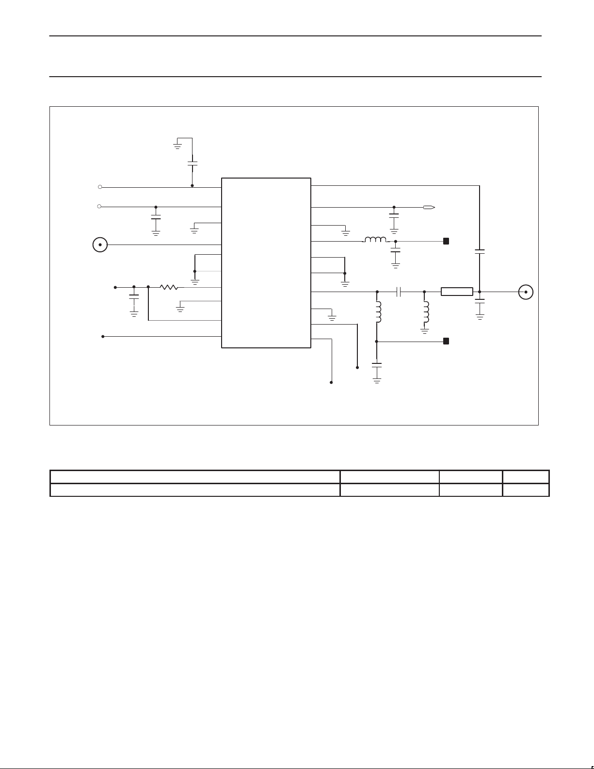
Figure 1. Application Diagram
ORDERING INFORMATION
DESCRIPTION TEMPERATURE RANGE ORDER CODE DWG #
20-Pin Plastic SSOP (Shrink Small Outline Package) -40 to +85°C SA910
SR01535
SOT266-1
1997 Aug 12
3
Page 4
Philips Semiconductors Product specification
SA910Variable gain RF predriver amplifier
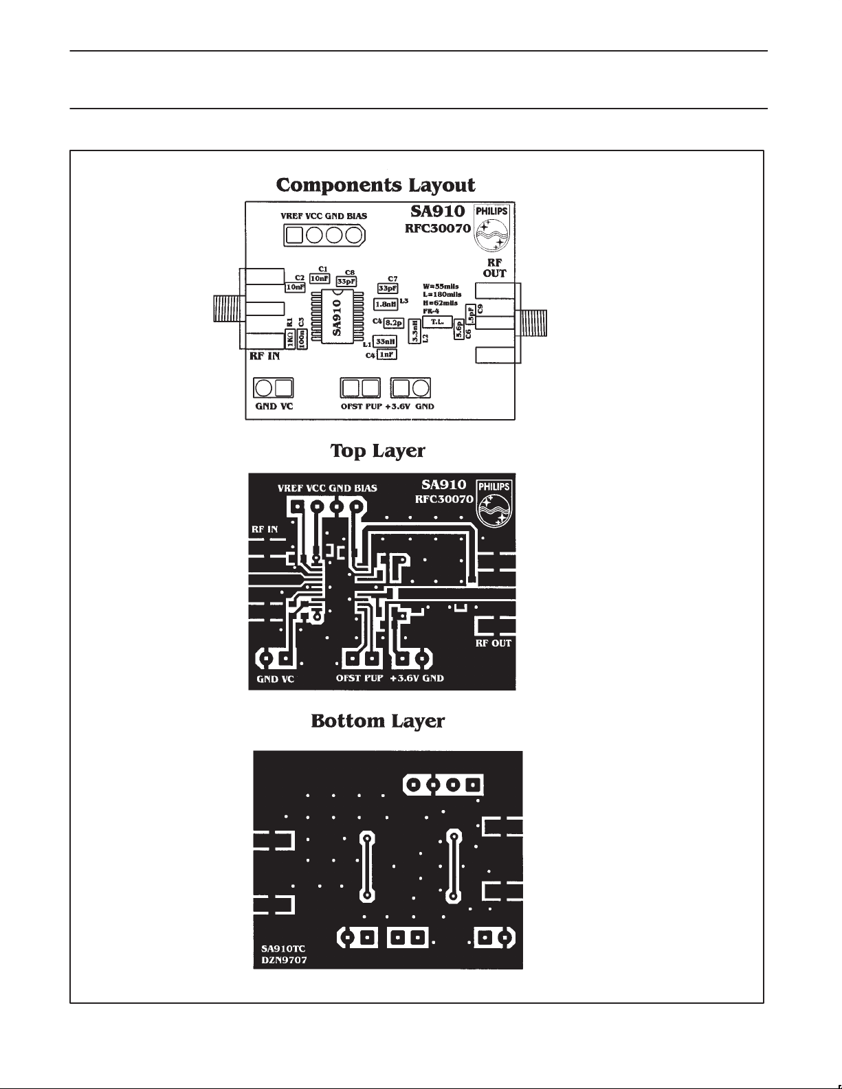
Notes:
All caps are MMC 0603,
Inductors: Toko LL2012
1997 Aug 12
SR01547
Figure 2. Application Board Layout of SA910
4
Page 5

Philips Semiconductors Product specification
SA910Variable gain RF predriver amplifier
130
L3 1.8nH
L1 33nH
C15
0.001uF
C21
0.1uF
C20
0.001uF
L4 3.9nH
L2 5.6nH
C24
0.001uF
C26
0.001uF
C25
0.1uF
C6 3.3pF
VCC2
ATTENUATOR/
SPLITTER
RFout
VPWRUP
VCC1
VREF
VCC1
VCC1
C23
C28
0.001uF
0.1uF
C27
0.001uF
R15 1K
RFin
VC
C13 0.
1000pf
C14
0.1uF
0 OHM RESI
4.7 uF
VREF
OUTLPF
RFIN
GND
VCCBIAS
VC
SA910
ON–CHIP
BIAS
EXTERNAL
AMP
BIAS
PSENSE
RFOUT1
GND
RFOUT2
BIASOUT
OFFSET
PWRUP
R19 10K
0 OHM RES
R17 10K
C24
0.001uF
C7 6.8pF
BLOCK DIAGRAM
OUTLPF
V
CC
V
CC
V
REF
RF
BIAS
GND
V
TO PSENSE
R9 18
R3 68 R8 16.9
R4
100
R5 100
R10 18
ATTENUATOR/SPLITTER
NETWORK
RFOUT
SR01548
Figure 3. Test Circuit Used In Characterizing SA910
1
EXTERNAL
AMP BIAS
A2A1
IN
ON-CHIP
C
BIAS
P
SENSE
RF
OUT
RF
OUT
GND
BIAS
OFFSET
PWRUP
1
2
OUT
SR01068
Figure 4. Block Diagram
1997 Aug 12
5
Page 6

Philips Semiconductors Product specification
SA910Variable gain RF predriver amplifier
PIN DESCRIPTIONS
Pin
No.
1 V
2 V
Mnemonic Function
CC1
REF
Power supply for power sense loop and off-chip bias
Power sense reference voltage input
3 GND Ground
4 RF
IN
Pre-driver input
5 GND Ground
6 GND Ground
7 OUTLPF Power sense detected output
8 GND Ground
9 VC Gain control input
10 VCC BIAS Power supply for on-chip bias
11 OFFSET External power amp bias offset adjustment
12 PWRUP Power-up input
13 GND Ground
14 RF
OUT2
Pre-driver output (open collector)
15 GND Ground
16 GND Ground
17 RF
OUT1
Output of first stage (open collector)
18 GND Ground
19 BIAS
20 P
SENSE
OUT
Output to bias external power amplifier stage
Power sense input
ABSOLUTE MAXIMUM RATINGS
SYMBOL PARAMETER RATING UNITS
VCC1/VCCBIAS DC supply voltages -0.3 to +6.0 V
1
-0.3 to (VCC1 + 0.3) V
P
T
P
P
DET
P
STG
Voltage applied to any other pin
D
IN
Power dissipation 1.0 W
Input drive power 5 mW
Input detect power 20 mW
L
Load power 500 mW
Storage temperature range -65 to +150
NOTE:
1. Except RF
OUT
1 and RF
2 which can have 8V max.
OUT
RECOMMENDED OPERATING CONDITIONS
SYMBOL PARAMETER RATING UNITS
VCC1/VCCBIAS Supply voltage 3 to 3.6 V
NOTE:
1. R
T
A
= 75° c/w
th
Operating ambient temperature range -40 to +85
°C
°C
1997 Aug 12
6
Page 7

Philips Semiconductors Product specification
SYMBOL
PARAMETER
TEST CONDITIONS
UNITS
PLLoad power at RF
Saturated
1
21.524dBm
SA910Variable gain RF predriver amplifier
AC ELECTRICAL CHARACTERISTICS
VCC1 = VCCBIAS = +3V;VCC(RF
stated.
f
Frequency range 820 830 905 MHz
RF
p
S
Small signal gain RFin = –20dBm 31 dB
21
η Power added efficiency PL = 24dBm 35 %
S
G
S
GOFF
Input return loss
11
Gain control range from V
C
Reverse isolation -40 dB
12
Gain at RF
(RFIN = -20dBm)
OUT2
PSENSE Power detector range 25 dB
NOTE:
1. Needs proper output matching.
OUT
OUT2
1, RF
2) = 3.6V; TA = 25°C, ZS = ZL = 50Ω; VC = 2V; RFIN = 0dBm @ 830MHz; unless otherwise
OUT
= 0.7 to 2V dP/dV <120dB/V 32 dB
c
during power-down
RFin = 0dBm
LIMITS
MIN TYP MAX
–12 dB
-30 dB
1997 Aug 12
7
Page 8

Philips Semiconductors Product specification
SYMBOL
PARAMETER
UNITS
IPUInput current to PWRUP
A
VPUInput level for PWRUP (Pin 12)
SA910Variable gain RF predriver amplifier
DC ELECTRICAL CHARACTERISTICS
VCC1 = VCCBIAS = +3V, VCC (RF
V
I
I
I
OFF
Power supply voltage range 2.7 3.0 5.5 V
CC
Total DC current from all V
CC
ICC under zero bias mode
ZB
Powerdown current Pin 12 = LOW 10 µA
p
p
V
V
I
I
REF
BIAS
BIAS
V
Input current to V
Power control reference voltage (Pin 1) 0 2.0 V
REF
Bias
voltage (Pin 19) (unadjusted) VC = 2.0V 0.68 V
OUT
DC current available @ Bias-OUT (Pin 19) 30 mA
Control voltage (Pin 9) range 0 2 V
C
OUT
1, RF
2) = 3.6V; TA = 25°C, ZS = ZL = 50Ω, ; unless otherwise stated.
OUT
TEST
CC
CONDITIONS
Pin 12 = HIGH;
Pin 9 > V
BE
MIN -3σ TYP +3σ MAX
Pin 12 = HIGH;
Pin 9 < V
BE
LIMITS
210 300 mA
0.7 mA
Pin 12 = HIGH 100
Pin 12 = LOW 10
Pin 12 = LOW 0 0.3V
Pin 12 = HIGH 0.7V
(Pin 2) 1 µA
REF
CC
CC
V
CC
µ
V
V
1997 Aug 12
8
Page 9

Philips Semiconductors Product specification
SA910Variable gain RF predriver amplifier
, V
dBm
1 = 3.0V
V
T = 25C, input Freq = 830 MHz
30
25
20
15
10
–8
–6
–4
–2
–20
–18
–16
–14
–12
dBm
–10
V = 3.0V, VC = 2.0V
CC
V = 5.5V, VC = 1.7V
CC
V = 2.7V, VC = 2.5V
CC
–0
SR01521
50
40
30
%
20
10
0
–20
CC
V = 2.0V
C
–16 –12 –8 –4
–18 –14 –10 –6 –2
Figure 8. PAE VS Input Power
Figure 5. Output Power VS Input Power
2 = 3.6V, INPUT FREQ = 830 MHZ
CC
dBm
T = 27C
T = 85C
T = –40C
0
SR01524
T = 25C, Pin = 0dBm
30
25
20
dBm
15
10
820
830
840
850
860
870
880
MHz
890
VCC = 3.0 V, VC = 2.0 V
VCC = 5.5 V, VC = 1.7 V
VCC = 2.7 V, VC = 2.5 V
Figure 6. Output Power VS Input Frequency
1 = 3.0V, V
V
CC
30
25
20
dBm
15
10
820 830 840 850 860 870 880 890 900
2 = 3.6V, Pin = 0dBm
CC
VC = 2.0V
MHz
T = 27C
T = 85C
T = –40C
Figure 7. Output Power VS Input Frequency
900
SR01522
SR01523
VCC1 = 3.0V
40
36
32
db
28
24
20
–20 –18 –16 –14 –12 –10 –8 –6 –4 –2 0
, V
2 = 3.6V, INPUT FREQ = 830 MHZ
CC
dbm
VC = 2.0V
T = 27C
T = 85C
T = –40C
Figure 9. Signal Gain VS Input Power
VCC1 = 3.0V
40
35
30
db
25
20
820 830 840 850 860 870
, V
2 = 3.6V, Pin = –20 dBm
CC
MHz
880
T = 27C
T = 85C
T = –40C
Figure 10. Signal Gain VS Input Frequency
SR01525
VC = 2.0V
890 900
SR01526
1997 Aug 12
9
Page 10

Philips Semiconductors Product specification
SA910Variable gain RF predriver amplifier
40
35
30
dB
25
20
–20 –18 –16 –14 –12 –10 –8 –6 –4 –2 0
T = 25C, Input Freq = 830 MHz, Pin = –20dBm
dBm
V =3.0V, VC = 2.0V
CC
V =5.5V, VC = 1.7V
CC
V =2.7V, VC = 2.5V
CC
Figure 11. Signal Gain VS Input Power
T = 25C, Pin = –20 dBm
40
35
dB
30
25
20
820
830
840
850
860
870
880
MHz
V =3.0V, VC = 2.0V
CC
V =5.5V, VC = 1.7V
CC
V =2.7V, VC = 2.5V
CC
Figure 12. Signal Gain VS Input Frequency
1 = 3.0V, VCC2 = 3.6V, INPUT FREQ = 830 MHZ
V
CC
30
V =2.0V
C
25
20
dBm
15
10
–20
–16
–12
–8
dBm
–4
Figure 13. Output Power VS Input Power
VCC1 = 3.0V, VCC2 = 3.6V, PIN = 0dBm
30
20
10
0
dBm
–10
–20
–30
–40
0.5
SR01527a
INPUT FREQ = 830 MHz
0.7
0.9
1.1
Volts
1.3
1.5
1.7
T = 27C
T = 27C
T = 85C
T = 85C
T = –40C
T = –40C
SR01530
2.0
Figure 14. Output Power VS VC
V
1 = 3.0V, VCC2 = 3.6V, Pin = 0 dBm
CC
INPUT FREQ = 830MHz
1
1.1
1.2
1.3
1.4
1.5
1.6
1.7
1.8
VOLTS
T = 27C
T = 85C
T = –40C
1.9
SR01531
2
890
900
SR01528
30
25
20
dBm
15
10
0.8
0.9
Figure 15. Output Power VS VREF (Closed Loop)
30
25
20
dBm
T = 27C
T = 85C
T = –40C
0
SR01529
15
10
0.8
Figure 16. Output Power VS VREF (Closed Loop)
T = 27C, INPUT FREQ = 830 MHz, PIN = 0 dBm
1
0.9
1.1
1.2
1.3
VOLTS
1.4
1.5
1.6
VCC = 3.0V
VCC = 5.5V
VCC = 2.7V
1.7
1.8
1.9
SR01537
2
1997 Aug 12
10
Page 11

Philips Semiconductors Product specification
SA910Variable gain RF predriver amplifier
40
35
30
25
20
%
15
10
5
–20
T = 25°C, Input Freq = 830 MHz
–16
–18
–12
–8 –4
dBm
VCC = 3.0 V, VC = 2.0 V
VCC = 5.5 V, VC = 1.7 V
VCC = 2.7 V, VC = 2.5 V
dB
–10
–20
–30
–40
–200–6–10–14
SR01532
VCC1 = 3.0V, VCC2 = 3.6V, T = 25°C
40
30
20
10
0
0.5
0.7
PIN = –20dBm@830 MHz
0.9
1.3
1.5
1.1
VC (VOLTS)
1.7
1.9
Figure 19. Small Signal Gain VS V
2.1
2.3
SR01534
2.5
C
Figure 17. PAE VS Input Power
POWER DISSIPATION (WATTS)1W
°C
(135 – T )
P =
D
A
75°C/W
0W
AMBIENT OPERATING TEMPERATURE
Figure 18. Power De–Rating Curve
135°C60°C
SR01533
1997 Aug 12
11
Page 12

Philips Semiconductors Product specification
SA910Variable gain RF predriver amplifier
SSOP20: plastic shrink small outline package; 20 leads; body width 4.4 mm SOT266-1
1997 Aug 12
12
Page 13

Philips Semiconductors Product specification
SA910Variable gain RF predriver amplifier
Data sheet status
Data sheet
status
Objective
specification
Preliminary
specification
Product
specification
Product
status
Development
Qualification
Production
Definition
This data sheet contains the design target or goal specifications for product development.
Specification may change in any manner without notice.
This data sheet contains preliminary data, and supplementary data will be published at a later date.
Philips Semiconductors reserves the right to make chages at any time without notice in order to
improve design and supply the best possible product.
This data sheet contains final specifications. Philips Semiconductors reserves the right to make
changes at any time without notice in order to improve design and supply the best possible product.
[1]
[1] Please consult the most recently issued datasheet before initiating or completing a design.
Definitions
Short-form specification — The data in a short-form specification is extracted from a full data sheet with the same type number and title. For
detailed information see the relevant data sheet or data handbook.
Limiting values definition — Limiting values given are in accordance with the Absolute Maximum Rating System (IEC 134). Stress above one
or more of the limiting values may cause permanent damage to the device. These are stress ratings only and operation of the device at these or
at any other conditions above those given in the Characteristics sections of the specification is not implied. Exposure to limiting values for extended
periods may affect device reliability.
Application information — Applications that are described herein for any of these products are for illustrative purposes only. Philips
Semiconductors make no representation or warranty that such applications will be suitable for the specified use without further testing or
modification.
Disclaimers
Life support — These products are not designed for use in life support appliances, devices or systems where malfunction of these products can
reasonably be expected to result in personal injury . Philips Semiconductors customers using or selling these products for use in such applications
do so at their own risk and agree to fully indemnify Philips Semiconductors for any damages resulting from such application.
Right to make changes — Philips Semiconductors reserves the right to make changes, without notice, in the products, including circuits, standard
cells, and/or software, described or contained herein in order to improve design and/or performance. Philips Semiconductors assumes no
responsibility or liability for the use of any of these products, conveys no license or title under any patent, copyright, or mask work right to these
products, and makes no representations or warranties that these products are free from patent, copyright, or mask work right infringement, unless
otherwise specified.
Philips Semiconductors
811 East Arques Avenue
P.O. Box 3409
Sunnyvale, California 94088–3409
Telephone 800-234-7381
Copyright Philips Electronics North America Corporation 1998
All rights reserved. Printed in U.S.A.
print code Date of release: 05-96
Document order number: 9397 750 03884
1997 Aug 12
13
 Loading...