

Page 1
80 SEG / 26 COM DRIVER & CONTROLLER FOR STN LCD
S6A0093
permission of LCD Driver IC Team.
Prepared by: Won-Sik, Kang
K2w3@samsung.co.kr
june. 2000.
Ver. 0.4
Contents in this document are subject to change without notice. No part of this document may be reproduced or
transmitted in any form or by any means, electronic or mechanical, for any purpose, without the express written
Page 2
80 SEG / 26 COM DRIVER & CONTROLLER FOR STN LCD S6A0093
S6A0093 Specification Revision History
Version Content Date
0.0 Original Jun.1998
0.1 Miss typed contents changed Jan.1999
0.2 RESETB pin VIL,VIH added Mar.1999
0.3 VDD change (2.4V~5.5V -> 2.4V~3.6V) Nov.1999
0.4 VDD change (2.4V~3.6V -> 2.4V~5.5V) Dec.1999
Inspection Jun.2000
1
Page 3

S6A0093 80 SEG / 26 COM DRIVER & CONTROLLER FOR STN LCD
CONTENTS
INTRODUCTION.......................................................................................................................................... 1
FEATURES ................................................................................................................................................. 1
BLOCK DIAGRAM ...................................................................................................................................... 3
PAD CONFIGURATION............................................................................................................................... 4
PAD CENTER COORDINATES...................................................................................................................5
PIN DESCRIPTION...................................................................................................................................... 6
POWER SUPPLY.................................................................................................................................6
LCD DRIVER SUPPLY......................................................................................................................... 6
SYSTEM CONTROL............................................................................................................................. 7
MPU INTERFACE ................................................................................................................................ 7
LCD DRIVER OUTPUTS...................................................................................................................... 8
TEST....................................................................................................................................................8
FUNCTION DESCRIPTION.......................................................................................................................... 9
SYSTEM INTERFACE..........................................................................................................................9
ADDRESS COUNTER (AC)................................................................................................................ 13
DISPLAY DATA RAM (DDRAM)......................................................................................................... 13
CHARACTER GENERATOR ROM (CGROM)..................................................................................... 13
CHARACTER GENERATOR RAM (CGRAM) ..................................................................................... 15
SEGMENT ICON RAM (ICONRAM).................................................................................................... 17
LOW POWER CONSUMPTION MODE .............................................................................................. 18
LCD DRIVER CIRCUIT....................................................................................................................... 18
INSTRUCTION DESCRIPTION .................................................................................................................. 19
INITIALIZING & POWER SAVE MODE SETUP......................................................................................... 29
HARDWARE RESET.......................................................................................................................... 29
INITIALIZING AND POWER SAVE SETUP......................................................................................... 30
LCD DRIVING POWER SUPPLY CIRCUIT................................................................................................ 33
VOLTAGE CONVERTER.................................................................................................................... 34
VOLTAGE REGULATOR .................................................................................................................... 35
ELECTRONIC CONTRAST CONTROL (32 STEPS)........................................................................... 36
VOLTAGE GENERATOR CIRCUIT .................................................................................................... 38
MPU INTERFACE...................................................................................................................................... 39
APPLICATION INFORMATION FOR LCD PANEL.................................................................................... 41
FRAME FREQUENCY............................................................................................................................... 43
MAXIMUM ABSOLUTE RATINGS............................................................................................................. 44
ELECTRICAL CHARACTERISTICS.......................................................................................................... 45
DC CHARACTERISTICS.................................................................................................................... 45
AC CHARACTERISTICS.................................................................................................................... 47
2
Page 4
80 SEG / 26 COM DRIVER & CONTROLLER FOR STN LCD S6A0093
INTRODUCTION
The S6A0093 is an LCD driver and controller LSI for liquid crystal dot matrix character display systems. It can
display 2 or 3 lines of 16 characters with 5 x 8 dots format. It is capable of interfacing various microprocessors,
supporting the 4-bit, 8-bit parallel modes and the clock synchronized serial mode. Voltage converter, oscillator,
voltage regulator, voltage follower and bias circuit are built in the IC. The double height character mode and line
vertical scroll functions are supported.
FEATURES
Driver Outputs
- Common outputs: 26 common
- Segment outputs: 80 segment
Applicable Panel Size
Font Display Duty Contents of outputs
2-line x 16 characters 1 / 17 2 x 16 characters + 80 icons
5 x 8
3-line x 16 characters 1 / 25 3 x 16 characters + 80 icons
Internal Memory
- Character Generator ROM (CGROM): 10,240 bits (256 characters x 5 x 8 dots)
- Character Generator RAM (CGRAM): 320 bits (8 characters x 5 x 8 dots)
- Display Data RAM (DDRAM): 512 bits (16 characters x 4 lines)
- Segment Icon RAM (ICONRAM): 80 bits (80 icons)
MPU Interface
- No busy MPU interface (no busy check or no execution waiting time)
- 8-bit parallel interface mode: 68-series and 80-series are available.
- 4-bit parallel interface mode: 68-series and 80-series are available.
- Serial interface mode: 4 pins clock synchronized serial interface
Function Set
- Various instruction set: display control, power save, power control, etc.
- COM / SEG bi-directional (4-type LCD application available)
- H/W reset (RESETB)
Built-in Analog Circuit
- Internal RC oscillator circuit or external clock
- Electronic volume for contrast control (32 steps)
- Voltage converter / voltage regulator / voltage follower & bias circuit
Low Power Operation
- Sleep mode operation (5µA Max.)
- Normal mode operation (80µA Max.)
1
Page 5

S6A0093 80 SEG / 26 COM DRIVER & CONTROLLER FOR STN LCD
Operating Voltage Range
- Power supply voltage (VDD): 2.4V ~ 5.5V
- LCD driving voltage (VLCD = V0 - VSS): 6.0V Max.
Package Type
- Gold bumped chip or TCP
2
Page 6
80 SEG / 26 COM DRIVER & CONTROLLER FOR STN LCD S6A0093
(DR)
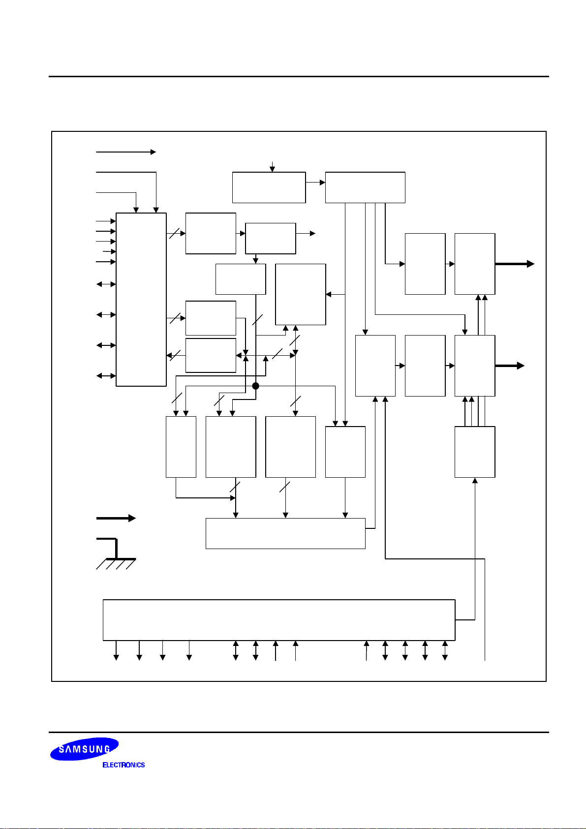
BLOCK DIAGRAM
RESETB
PS
IF
M I
CSB
RS
RW_WR
E_RD
DB7
(SI)
DB6
(SCL)
DB5-
DB4
DB3-
DB0
Parallel
Interface
4 bit/8 bit
Serial
Interface
Input Buffer
8
8
Data Output
8
8
Icon
RAM
80 bits
Instruction
Register
(IR)
Data
Register
Register
(OR)
5
Character
Generator
RAM
(CGRAM)
320 bits
Address
Counter
CK
Instruction
Decoder
Data RAM
(DDRAM)
7
8
Character
Generator
ROM
(CGROM)
10240 bits
Display
512 bits
8
8
Timing GeneratorOscillator
Cursor
and
Blink
Controlle
80 bits
Shift
Register
25 bits
Shift
Register
80 bits
Latch
Circuit
Common
Driver
Segment
Driver
LCD
Driver
Voltage
Selector
COM1-
COM24
COM I1
COM I2
SEG1-
SEG80
5 5
V
DD
GND
Voltage Converter Voltage Regulator Voltage Follower & Bias Resistor
CAP1+ CAP1- CAP2+ CAP2- VOUT V0 VEXT REF VR V1 V2 V3 V4 DIRS
Segment Data Conversion
LCD Driving Power Circuit
Figure 1. Block Diagram
3
Page 7
S6A0093 80 SEG / 26 COM DRIVER & CONTROLLER FOR STN LCD
............................
...
...
1
73
87
166
(-3065, -445)
(-2965, -405)
30
µ
m
30
µ
m
30
µ
m
60
µ
m
30
µ
m
42
µ
m
108
µ
m
42
µ
m
108
µ
m
(-3440, +740)
(+3440, +740)
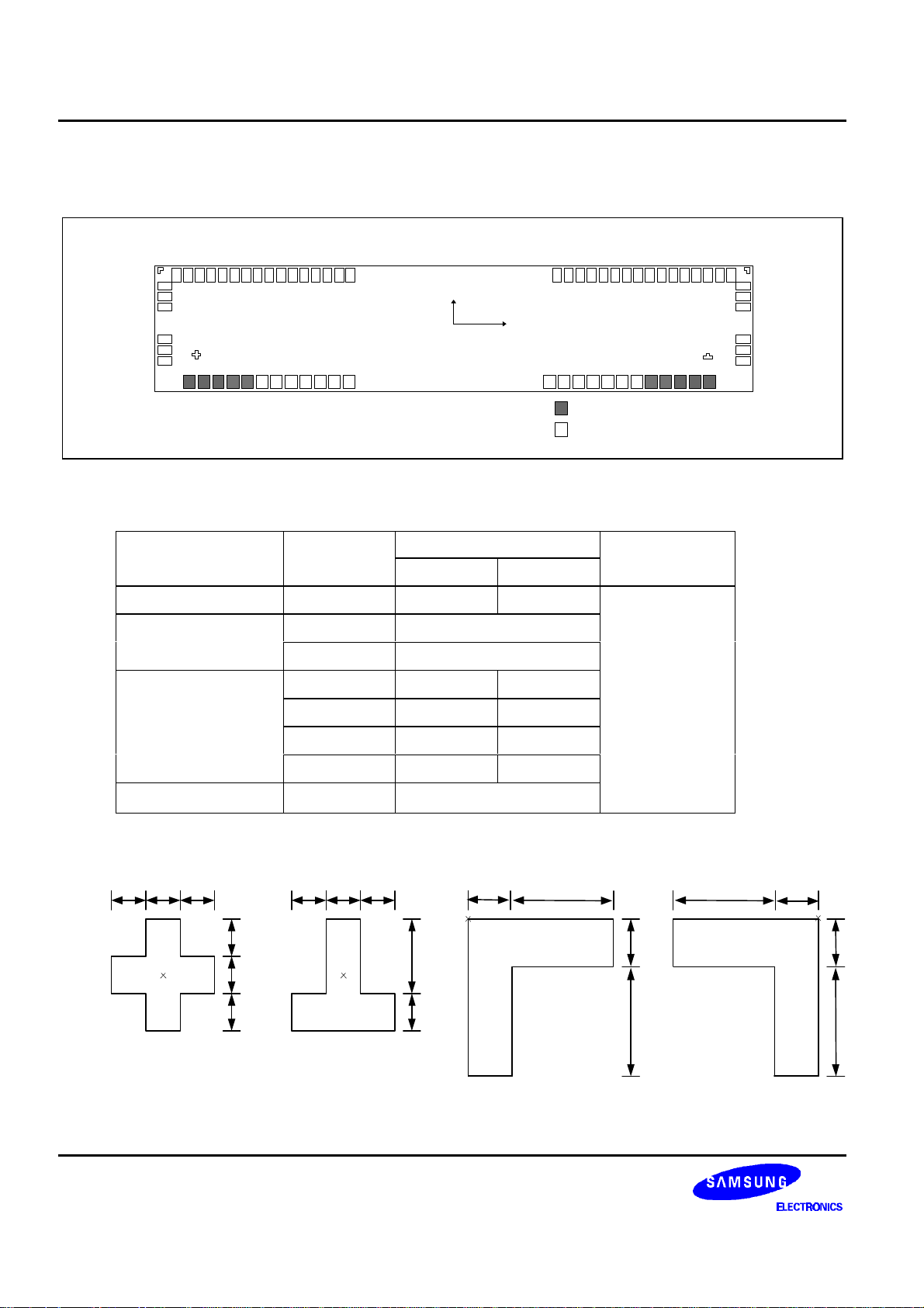
PAD CONFIGURATION
167
179
Y
(0,0)
...........................
Figure 2. Pad Configuration
Table 1. S6A0093 Pad Dimensions
Item Pad No.
Chip size - 7020 1620
1 ~ 73 90
Pad pitch
74 ~ 179 80
1 ~ 73 60 100
74 ~ 86 100 50
Bumped pad size
87 ~ 166 50 100
X Y
86
X
74
DUMMY PAD
PAD
Size
Unit
µm
167 ~ 179 100 50
Bumped pad height All pad 17
COG Align Key Coordinate ILB Align Key Coordinate
30µm 30µm 30µm
4
30µm 30µm 30µm
42µm 108µm
42µm108µm
Page 8
80 SEG / 26 COM DRIVER & CONTROLLER FOR STN LCD S6A0093
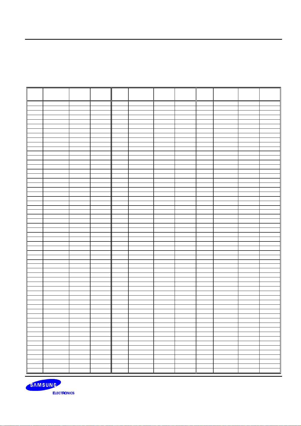
PAD CENTER COORDINATES
Table 2. Pad Center Coordinates
[Unit: µm]
Pad
No.
1
2
3
4
5
6
7
8
9
10
11
12
13
14
15
16
17
18
19
20
21
22
23
24
25
26
27
28
29
30
31
32
33
34
35
36
37
38
39
40
41
42
43
44
45
46
47
48
49
50
51
52
53
54
55
56
57
58
59
60
Pad
name
DUMMY
DUMMY
DUMMY
DUMMY
DUMMY
RS
VSS
RW_WR
VDD
E_RD
CSB
DB7
DB6
DB5
DB4
DB3
DB2
DB1
DB0
VDD
VDD
VDD
VSS
VSS
VSS
V4
V4
V3
V3
V2
V2
V1
V1
V0
V0
V0
V0
VR
VR
VOUT
VOUT
CAP2CAP2CAP2+
CAP2+
CAP1CAP1CAP1+
CAP1+
VEXT
VSS
VSS
VSS
REF
DIRS
VDD
VDD
VDD
CK
VSS
X Y
-3240
-3150
-3060
-2970
-2880
-2790
-2700
-2610
-2520
-2430
-2340
-2250
-2160
-2070
-1980
-1890
-1800
-1710
-1620
-1530
-1440
-1350
-1260
-1170
-1080
-990
-900
-810
-720
-630
-540
-450
-360
-270
-180
-90
0
90
180
270
360
450
540
630
720
810
900
990
1080
1170
1260
1350
1440
1530
1620
1710
1800
1890
1980
2070
-700
-700
-700
-700
-700
-700
-700
-700
-700
-700
-700
-700
-700
-700
-700
-700
-700
-700
-700
-700
-700
-700
-700
-700
-700
-700
-700
-700
-700
-700
-700
-700
-700
-700
-700
-700
-700
-700
-700
-700
-700
-700
-700
-700
-700
-700
-700
-700
-700
-700
-700
-700
-700
-700
-700
-700
-700
-700
-700
-700
Pad
No.
61
62
63
64
65
66
67
68
69
70
71
72
73
74
75
76
77
78
79
80
81
82
83
84
85
86
87
88
89
90
91
92
93
94
95
96
97
98
99
100
101
102
103
104
105
106
107
108
109
110
111
112
113
114
115
116
117
118
119
120
Pad
name
PS
VDD
IF
VSS
MI
VDD
RESETB
TEST
DUMMY
DUMMY
DUMMY
DUMMY
DUMMY
COMI1
COM1
COM2
COM3
COM4
COM5
COM6
COM7
COM8
COM17
COM18
COM19
COM20
SEG1
SEG2
SEG3
SEG4
SEG5
SEG6
SEG7
SEG8
SEG9
SEG10
SEG11
SEG12
SEG13
SEG14
SEG15
SEG16
SEG17
SEG18
SEG19
SEG20
SEG21
SEG22
SEG23
SEG24
SEG25
SEG26
SEG27
SEG28
SEG29
SEG30
SEG31
SEG32
SEG33
SEG34
X Y
2160
2250
2340
2430
2520
2610
2700
2790
2880
2970
3060
3150
3240
3400
3400
3400
3400
3400
3400
3400
3400
3400
3400
3400
3400
3400
3160
3080
3000
2920
2840
2760
2680
2600
2520
2440
2360
2280
2200
2120
2040
1960
1880
1800
1720
1640
1560
1480
1400
1320
1240
1160
1080
1000
920
840
760
680
600
520
-700
-700
-700
-700
-700
-700
-700
-700
-700
-700
-700
-700
-700
-520
-440
-360
-280
-200
-120
-40
40
120
200
280
360
440
700
700
700
700
700
700
700
700
700
700
700
700
700
700
700
700
700
700
700
700
700
700
700
700
700
700
700
700
700
700
700
700
700
700
Pad
No.
121
122
123
124
125
126
127
128
129
130
131
132
133
134
135
136
137
138
139
140
141
142
143
144
145
146
147
148
149
150
151
152
153
154
155
156
157
158
159
160
161
162
163
164
165
166
167
168
169
170
171
172
173
174
175
176
177
178
179
Pad
name
SEG35
SEG36
SEG37
SEG38
SEG39
SEG40
SEG41
SEG42
SEG43
SEG44
SEG45
SEG46
SEG47
SEG48
SEG49
SEG50
SEG51
SEG52
SEG53
SEG54
SEG55
SEG56
SEG57
SEG58
SEG59
SEG60
SEG61
SEG62
SEG63
SEG64
SEG65
SEG66
SEG67
SEG68
SEG69
SEG70
SEG71
SEG72
SEG73
SEG74
SEG75
SEG76
SEG77
SEG78
SEG79
SEG80
COMI2
COM24
COM23
COM22
COM21
COM16
COM15
COM14
COM13
COM12
COM11
COM10
COM9
X Y
440
360
280
200
120
40
-40
-120
-200
-280
-360
-440
-520
-600
-680
-760
-840
-920
-1000
-1080
-1160
-1240
-1320
-1400
-1480
-1560
-1640
-1720
-1800
-1880
-1960
-2040
-2120
-2200
-2280
-2360
-2440
-2520
-2600
-2680
-2760
-2840
-2920
-3000
-3080
-3160
-3400
-3400
-3400
-3400
-3400
-3400
-3400
-3400
-3400
-3400
-3400
-3400
-3400
700
700
700
700
700
700
700
700
700
700
700
700
700
700
700
700
700
700
700
700
700
700
700
700
700
700
700
700
700
700
700
700
700
700
700
700
700
700
700
700
700
700
700
700
700
700
440
360
280
200
120
40
-40
-120
-200
-280
-360
-440
-520
5
Page 9
S6A0093 80 SEG / 26 COM DRIVER & CONTROLLER FOR STN LCD
PIN DESCRIPTION
POWER SUPPLY
Table 3. Pin Description
Name I/O Description
VDD
Power
Power supply
Connect to MPU power supply pin.
VSS
V0
V1
V2
V3
V4
LCD DRIVER SUPPLY
Name I/O Description
CAP1+ O Capacitor + connecting pin for the internal voltage converter
CAP1- O Capacitor - connecting pin for the internal voltage converter
CAP2+ O Capacitor + connecting pin for the internal voltage converter
CAP2- O Capacitor - connecting pin for the internal voltage converter
VOUT I/O DC/DC voltage converter output (7.2V)
VR I
VEXT I
REF I
0V (GND)
Bias voltage level for LCD driving
Voltages should have the following relationship;
V0 ≥ V1 ≥ V2 ≥ V3 ≥ V4 ≥ VSS
When the built-in power circuit is active and internal 1/5 bias resistors are
used.
LCD bias
I/O
1/5 bias
When the built-in power circuit is active and internal 1/4 bias resistors are
used.
LCD bias
1/4 bias
Table 3. Pin Description (Continued)
Voltage adjust pin
This pin gives a voltage between V0 and VSS by resistance-division of
voltage.
External reference voltage for internal regulator (instead of the internal
VREF, 2V)
REF = "Low (VSS)": VEXT is not used (open).
REF = "High (VDD)": VEXT is reference input voltage of internal voltage
regulator.
Select the input voltage of internal voltage regulator
REF = "Low (VSS)": The input voltage of internal
Voltage regulator is the internal VREF(2V).
REF = "High (VDD)": The input voltage of internal
Voltage regulator is the voltage of VEXT.
V1 V2 V3 V4
(4/5) x V0 (3/5) x V0 (2/5) x V0 (1/5) x V0
V1 V2 V3 V4
(3/4) x V0 (2/4) x V0 (1/4) x V0
6
Page 10
80 SEG / 26 COM DRIVER & CONTROLLER FOR STN LCD S6A0093
SYSTEM CONTROL
Table 3. Pin Description (Continued)
Name I/O Description
External clock input. It must be fixed to "High" or "Low" when the internal
CK I
MI I
PS I
IF I
DIRS I
oscillation circuit is used. In case of the external clock mode, CK is used as the
clock and OS bit should be OFF.
MPU interface selection input
MI = "Low": 80-series MPU
MI = "High": 68-series MPU
Parallel / serial selection input
When PS = "Low": serial mode
When PS = "High": 4-bit / 8-bit bus mode
Interface data length selection pin for parallel data input
When PS = "Low"
IF = "Low" or "High": serial interface mode
When PS = High
IF = "Low": 4-bit bus mode
IF = "High": 8-bit bus mode
SEG direction selection input
When DIRS = "Low”
SEG1 → SEG2 → SEG79 → SEG80
When DIRS = "High”
SEG80 → SEG79 → SEG2 → SEG1
MPU INTERFACE
Table 3. Pin Description (Continued)
Name I/O Description
RESETB I
CSB I
RS I
RW_WR I
E_RD I
Reset input
S6A0093 is initialized while RESETB is low.
Chip selection input
S6A0093 is selected while CSB is low.
Register selection input
When RS = "Low", instruction register
When RS = "High", data register.
In 80-series MPU interface mode
This pin is connected to WR pin of MPU and is a active low write signal
In 68-series MPU interface mode
This pin is connected to R/W pin of MPU
When RW_WR = "Low", write mode
When RW_WR = "High", read mode
In 80-series MPU interface mode
This pin is connected to RD pin of MPU and is a active low read signal
In 68-series MPU interface mode
This pin is connected to E pin of MPU and enable read or write command
according to RW_WR signal.
7
Page 11
S6A0093 80 SEG / 26 COM DRIVER & CONTROLLER FOR STN LCD
Table 3. Pin Description (Continued)
Name I/O Description
DB0 ∼ DB3
DB4 ∼ DB5
DB6 (SCL),
DB7 (SI)
I/O When 8-bit bus mode, used as bi-directional data bus DB0 ∼ DB7
During 4-bit bus mode, only DB4 ∼ DB7 are used.
In this case DB0 ∼ DB3 pins are not used.
When serial mode, DB6 (SCL) is used as serial clock input pin and DB7 (SI) is
used as serial data input pin.
LCD DRIVER OUTPUTS
Table 3. Pin Description (Continued)
Name I/O Description
COM1 ∼ COM24
COMI1, COMI2 O
SEG1 ∼ SEG80
O Common signal output for driving LCD
Common signal output for icon display
These are the same signal but the name is different.
O Segment signal output for driving LCD
TEST
Table 3. Pin Description (Continued)
Name I/O Description
Test pin
TEST I
This pin is not used for normal operation.
TEST: Open
NOTE: DUMMY – These pins should be opened (floated).
8
Page 12
80 SEG / 26 COM DRIVER & CONTROLLER FOR STN LCD S6A0093
FUNCTION DESCRIPTION
SYSTEM INTERFACE
S6A0093 has two kinds of interface type with MPU: bus mode, serial mode. Serial or bus mode is selected by PS pin.
In bus mode, 4-bit bus or 8-bit bus is selected by IF pin, and 68 series MPU or 80 series MPU is selected by MI pin.
Table 4. Various Kinds of MPU Interface according to PS, MI and IF
PS MI IF CSB RS RW_WR E_RD DB0∼DB3 DB4∼DB5 DB6 DB7
68 series
Bus mode
(H)
Serial
mode
(L)
NOTES:
1. Don’ t care (high, low or open)
2. Fixed high (VDD) or low (VSS)
(H)
80 series
(L)
(H)/(L)
8 bit (H) CSB RS R/W E DB0∼DB3 DB4∼DB5 DB6 DB7
4 bit (L) CSB RS R/W E ∗
8 bit (H) CSB RS WR RD DB0∼DB3 DB4∼DB5 DB6 DB7
4 bit (L) CSB RS WR RD
(2)
(H)/(L) CSB RS (H)/(L) (H)/(L)
(1)
∗
∗ ∗
DB4∼DB5 DB6 DB7
DB4∼DB5 DB6 DB7
SCL SI
PS: "High" = bus mode, "Low" = serial mode
MI: "High" = 68-series MPU, "Low" = 80-series MPU
IF: "High" = 8 bit mode, "Low" = 4 bit mode (PS: "High")
CSB: "High" = chip is not selected, "Low" = chip is selected
RS: "High" = data register, "Low" = instruction register
RW_WR: Read / Write indicating signal in 68 mode or active low signal for enabling write in 80 mode
E_RD: Active high signal for enabling command is 68 mode or active low signal for enabling read in 80 mode.
SCL (DB6): Serial clock input
SI (DB7): Serial data input
9
Page 13
S6A0093 80 SEG / 26 COM DRIVER & CONTROLLER FOR STN LCD
MI
CSB
RS
RW_WR
E_RD
DB7∼DB0
Data
IF
Interface with MPU in Parallel Mode (PS = "High")
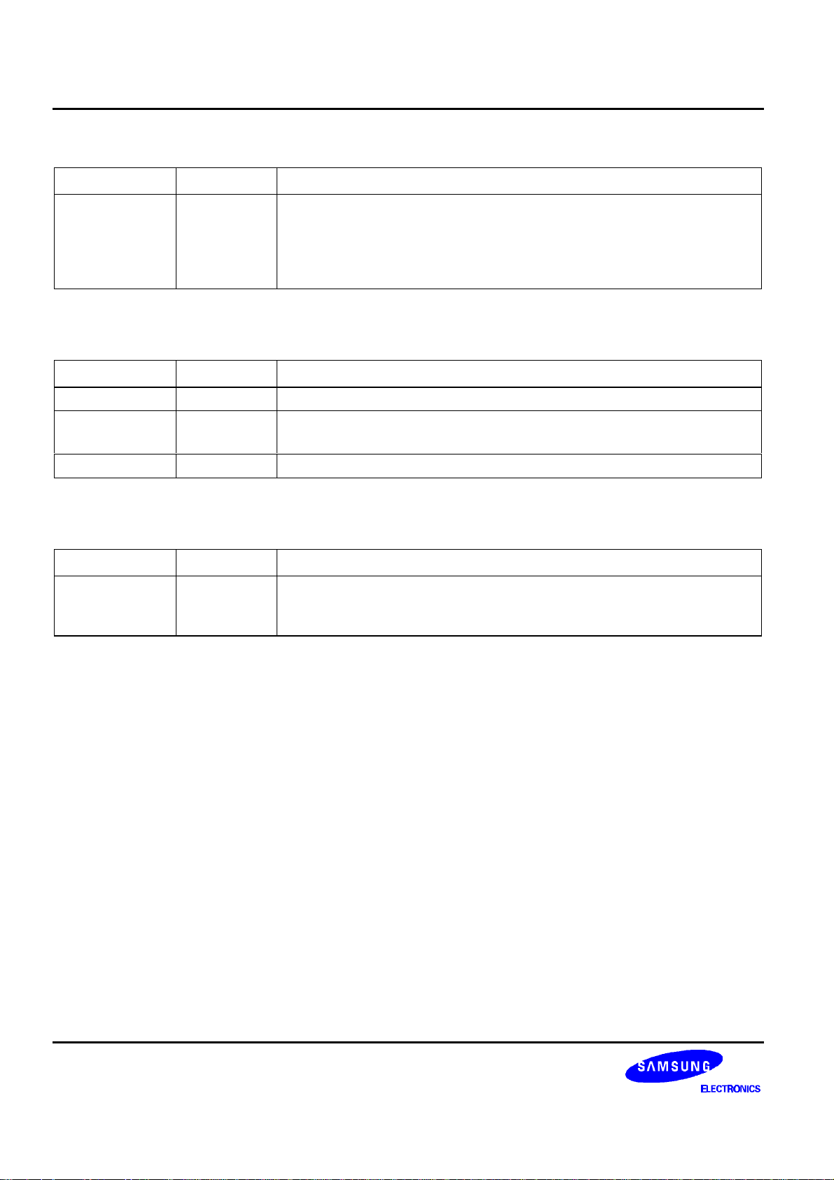
During writing operation, two 8-bit registers, data register (DR) and instruction register (IR), are used. The data
register (DR) is used as temporary data storage place for being written into DDRAM / CGRAM / ICONRAM and one
of these RAMs is selected by RAM address setting instruction. The Instruction register (IR) is used only to store
instruction code transferred from MPU. To select DR or IR register, RS input pin is used.
During reading operation, 8-bit register, output data register (OR) is used. The output data register (OR) is used as
temporary data storage place for being read from DDRAM / CGRAM / ICONRAM and one of these RAMs is selected
by RAM address setting instruction. After RAM address setting, first reading is a dummy cycle in 8-bit bus mode
(figure 3, 4). The valid data comes from second reading. In 4-bit bus mode, after RAM address setting, first and
second reading are dummy cycles (figure 5, 6). The valid data comes from third reading. The dummy read make the
address counter (AC) increased by 1. So it is recommended to set address again before writing. The instruction read
cycle is not supported and it is regarded as a no operation cycle.
In 4-bit bus mode, it is needed to transfer 4-bit data (through DB7∼DB4) by two times. The high order bits (for 8-bit
mode DB7∼DB4) are written before the low order bits (for 8-bit mode DB3∼DB0) in write and low order bits (for 8-bit
mode DB3∼DB0) are read before the high order bits (for 8-bit mode DB7∼DB4) in read transaction. The DB0∼DB3
pins are floated in this 4-bit bus mode. After RESETB resets, S6A0093 considers first 4-bit data from MPU as the
high order bits.
Valid
Instruction
NOP RAM
Dummy
Data
Figure 3. Timing Diagram of 8-bit Parallel Bus Mode Data Transfer (68-series MPU Mode)
10
Page 14
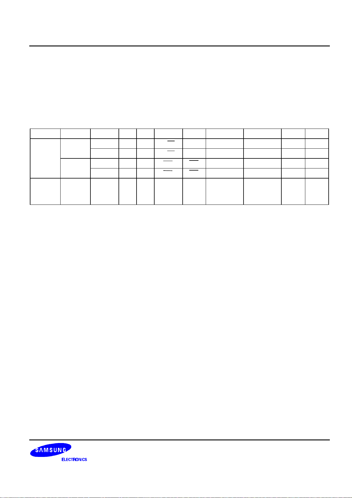
80 SEG / 26 COM DRIVER & CONTROLLER FOR STN LCD S6A0093
MI
CSB
RS
RW_WR
E_RD
DB7∼DB0
Data
MI
CSB
RS
RW_WR
E_RD
DB7∼DB4
4-bit
4-bit
4-bit
4-bit
4-bit
4-bit
IF
MI
CSB
RS
RW_WR
E_RD
DB7∼DB4
4-bit
4-bit
4-bit
4-bit
4-bit
4-bit
IF
IF
Valid
Instruction
NOP RAM
Dummy
Data
Figure 4. Timing Diagram of 8-bit Parallel Bus Mode Data Transfer (80-series MPU Mode)
upper
lower
Instruction Write Dummy Read Data WriteNOP
lower
upper
upper
lower
Figure 5. Timing Diagram of 4-bit Parallel Bus Mode Data Transfer (68-series MPU Mode)
upper
lower
lower
upper
upper
lower
Instruction Write Dummy Read Data WriteNOP RAM Read
Figure 6. Timing Diagram of 4-bit Parallel Bus Mode Data Transfer (80-series MPU Mode)
11
Page 15
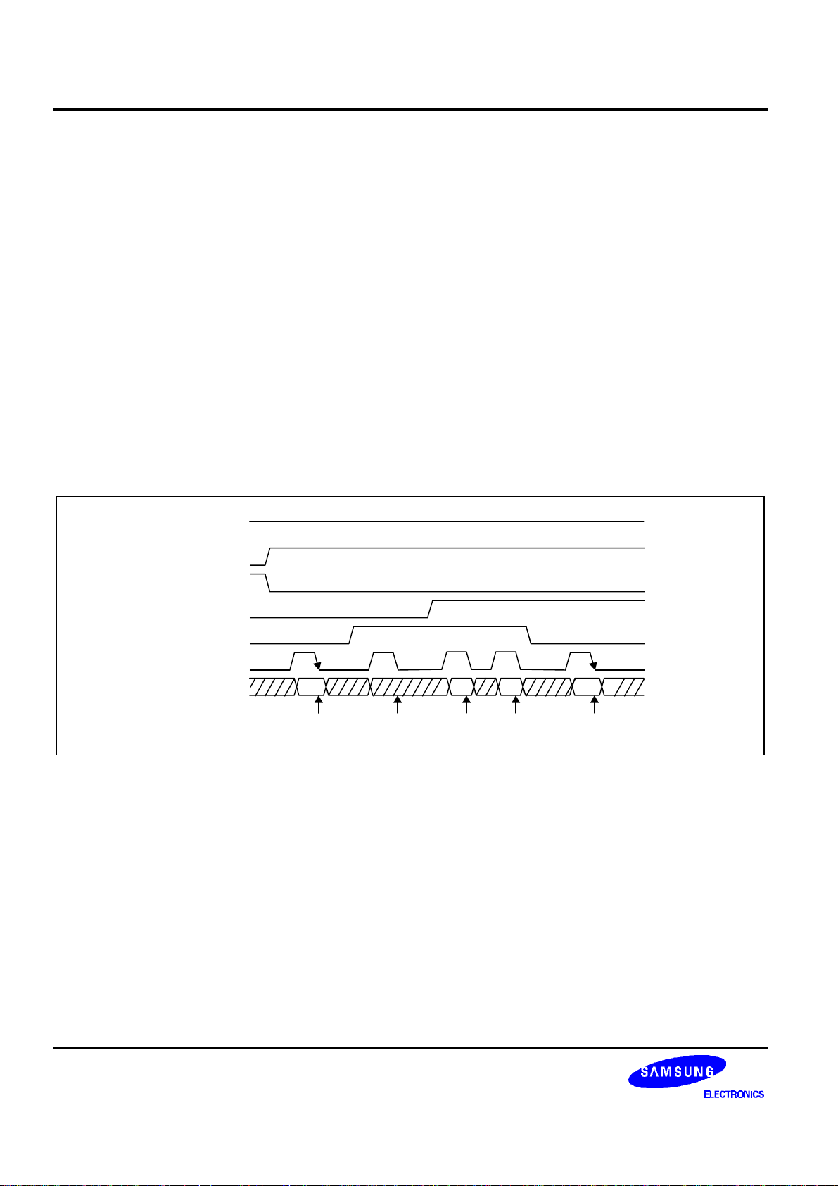
S6A0093 80 SEG / 26 COM DRIVER & CONTROLLER FOR STN LCD
RS
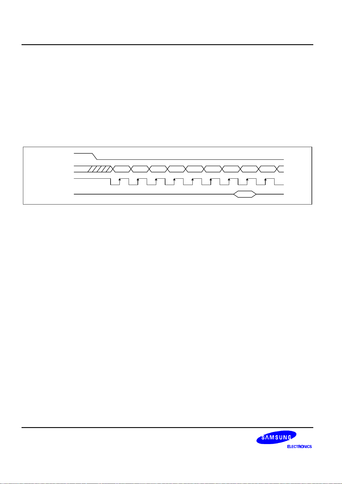
Interface with MPU in Serial Mode (PS = "Low")
When PS input pin is "Low", clock synchronized serial interface mode is selected. At this time, five ports, RESETB
(reset input), SCL (DB6, synchronizing transfer clock), SI (DB7, serial input data), RS (register selection input) and
CSB(chip selection input) are used.
By setting CSB to "Low", S6A0093 can receive SCL input. If CSB is set to "High", S6A0093 resets the internal 8-bit
shift register and 3-bit counter. Serial data is input in the order of "D7, D6, D5, D4, D3, D2, D1, D0" from the serial
data input pin (SI = DB7) at the rising edge of serial clock (SCL = DB6).
At the rising edge of the 8th serial clock, the serial data (D7-D0) is converted into 8 bit bus mode data. The RS input
of the DR/IR selection is latched at the rising edge of the 8th serial clock (SCL).
CSB
SI (DB7)
SCL (DB6)
D7 D6 D5 D4 D3 D2 D1 D0 D7
1 2 3 4 5 6 7 8 9
Figure 7. Timing Diagram of Serial Data Transfer
12
Page 16
80 SEG / 26 COM DRIVER & CONTROLLER FOR STN LCD S6A0093
ADDRESS COUNTER (AC)
Address Counter (AC) in S6A0093 stores DDRAM/ CGRAM/ ICONRAM address. After writing into or reading from
DDRAM / CGRAM / ICONRAM, AC is automatically increased by 1. The address counter is only one and stores the
address among DDRAM / CGRAM / ICONRAM.
DISPLAY DATA RAM (DDRAM)
DDRAM stores display data of maximum 64 x 8 bits (Max. 64 characters). DDRAM address is set in the address
counter (AC) as a hexadecimal number.
1st Ch. 16th Ch.
COM1 ∼ COM8
COM9 ∼ COM16
Hidden Line
Hidden Line
SEG1 SEG80
COM1 ∼ COM8
COM9 ∼ COM16
COM17 ∼ COM24
Hidden Line
SEG1 SEG80
04 05 06 07 08 09 0A 0B 0C 0D 0E 0F00 01 02 03
14 15 16 17 18 19 1A 1B 1C 1D 1E 1F10 11 12 13
24 25 26 27 28 29 2A 2B 2C 2D 2E 2F20 21 22 23
34 35 36 37 38 39 3A 3B 3C 3D 3E 3F30 31 32 33
(1) 2 line mode DDRAM Address
04 05 06 07 08 09 0A 0B 0C 0D 0E 0F00 01 02 03
14 15 16 17 18 19 1A 1B 1C 1D 1E 1F10 11 12 13
24 25 26 27 28 29 2A 2B 2C 2D 2E 2F20 21 22 23
34 35 36 37 38 39 3A 3B 3C 3D 3E 3F30 31 32 33
(2) 3 line mode DDRAM Address
Figure 8. DDRAM Address
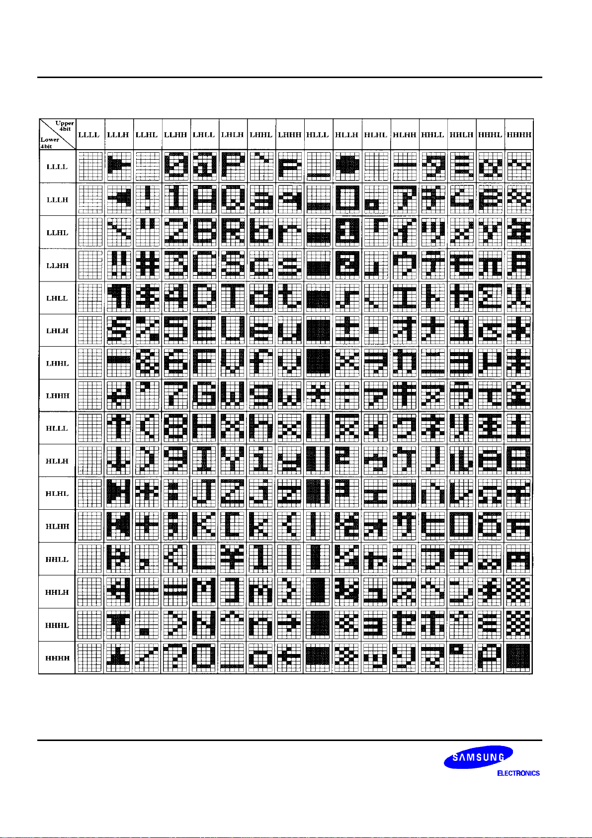
CHARACTER GENERATOR ROM (CGROM)
CGROM has 5 x 8-dot 256 characters. The CG bit of the instruction table selects the 8 characters (00h ~ 07h) of
CGROM or CGRAM.
13
Page 17
S6A0093 80 SEG / 26 COM DRIVER & CONTROLLER FOR STN LCD
Table 5. CGROM Character Code (00)
14
Page 18

80 SEG / 26 COM DRIVER & CONTROLLER FOR STN LCD S6A0093
CHARACTER GENERATOR RAM (CGRAM)
CGRAM has up to 5 x 8-dot 8 characters. By writing font data to CGRAM, user defined character can be used.
CGRAM can be written regardless of CG bit.
Table 6. Relationship between Character Code (DDRAM) and Character Pattern (CGRAM)
Character code
(DDRAM data)
D7 D6 D5 D4 D3 D2 D1 D0 A6 A5 A4 A3 A2 A1 A0 P7 P6 P5 P4 P3 P2 P1 P0
0 0 0 0 0 0 0 0
(00h)
0 0 0 0 0 0 0 1
(01h)
0 0 0 0 0 0 1 0
(02h)
0 0 0 0 0 0 1 1
(03h)
DD/CGRAM address CGRAM data
1 0 0 0 0 0 0
1 0 0 0 0 0 1
1 0 0 0 0 1 0
1 0 0 0 0 1 1
1 0 0 0 1 0 0
1 0 0 0 1 0 1
1 0 0 0 1 1 0
1 0 0 0 1 1 1
1 0 0 1 0 0 0
1 0 0 1 0 0 1
1 0 0 1 0 1 0
1 0 0 1 0 1 1
1 0 0 1 1 0 0
1 0 0 1 1 0 1
1 0 0 1 1 1 0
1 0 0 1 1 1 1
1 0 1 0 0 0 0
1 0 1 0 0 0 1
1 0 1 0 0 1 0
1 0 1 0 0 1 1
1 0 1 0 1 0 0
1 0 1 0 1 0 1
1 0 1 0 1 1 0
1 0 1 0 1 1 1
1 0 1 1 0 0 0
1 0 1 1 0 0 1
1 0 1 1 0 1 0
1 0 1 1 0 1 1
1 0 1 1 1 0 0
1 0 1 1 1 0 1
1 0 1 1 1 1 0
1 0 1 1 1 1 1
- - - 0 1 0 1 0
- - - 1 0 1 0 1
- - - 0 1 0 1 0
- - - 1 0 1 0 1
- - - 0 1 0 1 0
- - - 1 0 1 0 1
- - - 0 1 0 1 0
- - - 1 0 1 0 1
- - - 0 0 0 0 0
- - - 1 1 1 1 1
- - - 0 0 0 0 0
- - - 1 1 1 1 1
- - - 0 0 0 0 0
- - - 1 1 1 1 1
- - - 0 0 0 0 0
- - - 1 1 1 1 1
- - - 0 1 0 1 0
- - - 0 1 0 1 0
- - - 0 1 0 1 0
- - - 0 1 0 1 0
- - - 0 1 0 1 0
- - - 0 1 0 1 0
- - - 0 1 0 1 0
- - - 0 1 0 1 0
- - - 0 1 1 1 0
- - - 1 0 1 0 1
- - - 1 1 0 1 1
- - - 1 0 1 0 1
- - - 0 1 1 1 0
- - - 1 1 1 1 1
- - - 1 1 1 1 1
- - - 1 1 1 1 1
Pattern
number
Pattern 1
Pattern 2
Pattern 3
Pattern 4
15
Page 19

S6A0093 80 SEG / 26 COM DRIVER & CONTROLLER FOR STN LCD
Table 6. Relationship between Character Code (DDRAM) and Character Pattern (CGRAM) (continued)
Character code
(DDRAM data)
D7 D6 D5 D4 D3 D2 D1 D0 A6 A5 A4 A3 A2 A1 A0 P7 P6 P5 P4 P3 P2 P1 P0
0 0 0 0 0 1 0 0
(04h)
0 0 0 0 0 1 0 1
(05h)
0 0 0 0 0 1 1 0
(06h)
0 0 0 0 0 1 1 1
(07h)
NOTE: "-" - Don’ t care
DD/CGRAM address CGRAM data
1 1 0 0 0 0 0
1 1 0 0 0 0 1
1 1 0 0 0 1 0
1 1 0 0 0 1 1
1 1 0 0 1 0 0
1 1 0 0 1 0 1
1 1 0 0 1 1 0
1 1 0 0 1 1 1
1 1 0 1 0 0 0
1 1 0 1 0 0 1
1 1 0 1 0 1 0
1 1 0 1 0 1 1
1 1 0 1 1 0 0
1 1 0 1 1 0 1
1 1 0 1 1 1 0
1 1 0 1 1 1 1
1 1 1 0 0 0 0
1 1 1 0 0 0 1
1 1 1 0 0 1 0
1 1 1 0 0 1 1
1 1 1 0 1 0 0
1 1 1 0 1 0 1
1 1 1 0 1 1 0
1 1 1 0 1 1 1
1 1 1 1 0 0 0
1 1 1 1 0 0 1
1 1 1 1 0 1 0
1 1 1 1 0 1 1
1 1 1 1 1 0 0
1 1 1 1 1 0 1
1 1 1 1 1 1 0
1 1 1 1 1 1 1
- - - 1 1 0 1 1
- - - 1 0 0 0 1
- - - 0 0 0 0 0
- - - 1 0 0 0 1
- - - 1 1 0 1 1
- - - 1 1 1 1 1
- - - 1 1 1 1 1
- - - 1 1 1 1 1
- - - 1 1 1 1 1
- - - 1 1 1 1 1
- - - 0 0 0 0 0
- - - 0 0 0 0 0
- - - 1 1 1 1 1
- - - 1 1 1 1 1
- - - 0 0 0 0 0
- - - 0 0 0 0 0
- - - 0 0 1 1 0
- - - 0 0 1 1 0
- - - 0 0 1 1 0
- - - 0 0 1 1 0
- - - 0 0 1 1 0
- - - 0 0 1 1 0
- - - 0 0 1 1 0
- - - 0 0 1 1 0
- - - 0 0 0 0 0
- - - 1 0 0 0 1
- - - 1 1 0 1 1
- - - 1 0 0 0 1
- - - 0 0 0 0 0
- - - 1 0 0 0 1
- - - 1 1 0 1 1
- - - 1 1 1 1 1
Pattern
number
Pattern 5
Pattern 6
Pattern 7
Pattern 8
16
Page 20

80 SEG / 26 COM DRIVER & CONTROLLER FOR STN LCD S6A0093
SEG 5
SEG 4
SEG 3
SEG 2
SEG 1
SEG 80
SEG 79
SEG 78
SEG 77
SEG 76
SEGMENT ICON RAM (ICONRAM)
ICONRAM has segment control data and segment pattern data. COMI1 and COMI2 are the same signal but the
name is different. So the icons on the same SEG are displayed at the same time. The number of icons is 80.
COMI 1
COMI 2
ICONRAM address
NOTE: "-" - Don’ t care
Figure 9. Relationship between ICONRAM and Icon Display
Table 7. Relationship between ICONRAM Address and Display Pattern
ICONRAM bits
D7 D6 D5 D4 D3 D2 D1 D0
00h - - - S1 S2 S3 S4 S5
01h - - - S6 S7 S8 S9 S10
02h - - - S11 S12 S13 S14 S15
.
.
.
.
.
.
.
.
.
.
.
.
.
.
.
.
.
.
0Dh - - - S66 S67 S68 S69 S70
0Eh - - - S71 S72 S73 S74 S75
0Fh - - - S76 S77 S78 S79 S80
17
Page 21

S6A0093 80 SEG / 26 COM DRIVER & CONTROLLER FOR STN LCD
LOW POWER CONSUMPTION MODE
S6A0093 provides with sleep mode for saving power consumption during standby period.
Sleep Mode (Power Save Bit ON, Oscillation Bit OFF)
To enter the sleep mode, the power circuit and oscillation circuit should be turned off by using the power save
command and the power control command. This mode helps to save power consumption by reducing current to
reset level.
1. Liquid Crystal Display Output
COM1 ~ COM24, COMI1, COMI2: VSS level
SEG1 ~ SEG80: VSS level
2. Data written in DDRAM, CGRAM, ICONRAM and registers are remained as previous value.
3. Operation mode is retained the same as it was prior to execution of the sleep mode.
All internal circuits are stopped.
4. Power Circuit and Oscillation Circuit
The built-in power supply circuit and oscillation circuit are turned off by power save command and
power control command.
LCD DRIVER CIRCUIT
LCD Driver circuit has 26 common and 80 segment signals for driving LCD. Data from ICONRAM/ CGRAM/
CGROM are transferred to 80-bit segment register serially, and then they are stored to 80-bit shift latch. In case of
2-line display mode, COM1 ~ COM16, COMI1 and COMI2 have 1/17 duty, and in 3-line mode, COM1 ~ COM24,
COMI1 and COMI2 have 1/25 duty ratio. SEG bi-directional function is selected by DIRS input pin, and COM shift
direction is selected by function set instruction "S" bit.
Table 8. SEG Data Shift Direction
DIRS pin SEG data shift direction
Low SEG1 → SEG2 → SEG3 ....…………………….............. SEG78 → SEG79 → SEG80
High
Line
mode
2-line
mode
SEG80 → SEG79 → SEG78 .......…………………........... SEG3 → SEG2 → SEG1
Table 9. COM Data Shift Direction
S COM data shift direction
0 (left) COM1 → COM2 ......………….... COM15 → COM16 → COMI1 (COMI2)
1 (right) COMI1 (COMI2) → COM16 → COM15 ....…………........ COM2 → COM1
18
3-line
mode
0 (left) COM1 → COM2 ...…………....... COM23 → COM24 → COMI1 (COMI2)
1 (right) COMI1 (COMI2) → COM24 → COM23 .....……………... COM2 → COM1
Page 22

80 SEG / 26 COM DRIVER & CONTROLLER FOR STN LCD S6A0093
INSTRUCTION DESCRIPTION
Table 10. Instruction Table
Instruction RS DB7 DB6 DB5 DB4 DB3 DB2 DB1 DB0 Description
Return
home
Double
height mode
Power
save
Function
set
Line shift
mode
Bias control 0 0 0 0 1 1 1 - BS
Power
control
0 0 0 0 0 0 0 1 -
0 0 0 0 0 1 0 DH2 DH1
0 0 0 0 0 1 1 OS PS
0 0 0 0 1 0 N S CG
0 0 0 0 1 1 0 LS2 LS1
0 0 0 1 0 0 VC VR VF
DDRAM address is set to 00h from AC and the cursor returns
to 00h position
The contents of DDRAM are not changed.
Double height mode
DH2, DH1 = 00: normal display (default)
01: COM1 ∼ COM16 is a double height,
COM17∼COM24 is normal
10: 1) 2-line mode : normal display
2) 3-line mode : COM1∼COM8 is normal,
COM9 ∼ COM24 is a double
height
11: normal display
Power save / oscillation circuit ON / OFF
OS = 0: oscillator OFF (default) 1: oscillator ON
PS = 0: power save OFF (default) 1: power save ON
Display line mode
N = 0: 2-line display mode (default) 1: 3-line display mode
shifting direction of COM.
S = 0: 1) 2-line mode: COM1 -> COM16 (default)
2) 3-line mode: COM1 -> COM24 (default)
1: 1) 2-line mode: COM16 -> COM1
2) 3-line mode: COM24 -> COM1
Select CGRAM or CGROM
CG = 0: CGROM (default) 1: CGRAM
Determination of the DDRAM line which is displayed at the first
line at LCD
LS2, LS1 = 00: DDRAM line 1 shows at the first line of
LCD (default).
01: DDRAM line 2 shows at the first line of LCD.
10: DDRAM line 3 shows at the first line of LCD.
11: DDRAM line 4 shows at the first line of LCD
Determination of bias
BS = 0: 1/5 bias (default)
1: 1/4 bias
LCD power control
VC = 0: voltage converter OFF (default)
1: voltage converter ON
VR = 0: voltage regulator OFF (default)
1: voltage regulator ON
VF = 0: voltage follower OFF (default)
1: voltage follower ON
19
Page 23

S6A0093 80 SEG / 26 COM DRIVER & CONTROLLER FOR STN LCD
Table 10. Instruction Table (Continued)
Instruction RS DB7 DB6 DB5 DB4 DB3 DB2 DB1 DB0 Description
Cursor / blink / display ON / OFF
Display
control
DD/CGRAM
address
set
ICONRAM
address
set
Write
Data
Read
Data
NOP 0 0 0 0 0 0 0 0 0 Non-operation Instruction
Test 0 0 0 1 1 * * * * Don’ t use this Instruction.
0 0 0 1 0 1 C B D
0 1 AC6 AC5 AC4 AC3 AC2 AC1 AC0
0 0 1 0 IA4 IA3 IA2 IA1 IA0
1 D7 D6 D5 D4 D3 D2 D1 D0 Write DDRAM / CGRAM / ICONRAM
1 D7 D6 D5 D4 D3 D2 D1 D0 Read DDRAM / CGRAM / ICONRAM or registers data
NOTES:
1. "-": Don’ t care
2. "*": Don’ t use
3: Instruction execution time depends on the internal process time of S6A0093, therefore it is necessary to provide a time larger
than one MPU interface cycle time (tc) between execution of two successive instructions.
C = 0: cursor OFF (default), 1: cursor ON
B = 0: blink OFF (default), 1: blink ON
D = 0: display OFF (default), 1: display ON
DDRAM / CGRAM address
range: DDRAM 00h ∼ 3Fh
CGRAM 40h ∼ 7Fh
ICONRAM address, electronic volume and test byte address
range: ICONRAM 00h ∼ 0Fh
EV 10h (electronic volume byte), TE 11h (test byte)
(NOTE1)
20
Page 24

80 SEG / 26 COM DRIVER & CONTROLLER FOR STN LCD S6A0093
Return Home
RS DB7 DB6 DB5 DB4 DB3 DB2 DB1 DB0
0 0 0 0 0 0 0 1 -
Return Home instruction field makes cursor return home.
DDRAM address is set to 00h from AC and the cursor returns to 00h position. The contents of DDRAM are not
changed.
Double Height Mode
RS DB7 DB6 DB5 DB4 DB3 DB2 DB1 DB0
0 0 0 0 0 1 0 DH2 DH1
Double Height mode instruction field selects double height line type.
DH2, DH1 = 00: normal display line mode (default)
01: COM1 ∼ COM16 is a double height,
COM17 ∼ COM24 is normal
10: 1) 2-line mode: normal display
2) 3-line mode: COM1 ∼ COM8 is normal
COM9 ∼ COM24 is a double height
11: normal display
Figure 11. COM1 ~ 16 is a Double Height Line, COM17 ~ 24 is Normal (DH2, DH1 = 01)
Figure 10. 3 Line Normal Mode Display (DH2, DH1 = 00)
21
Page 25

S6A0093 80 SEG / 26 COM DRIVER & CONTROLLER FOR STN LCD
Figure 12. COM1 ~ 8 is Normal, COM9 ~ COM24 is a Double Height Line (DH2, DH1 = 10)
Figure 13. 2-line Normal Mode Display (DH2, DH1 = 00)
Figure 14. COM1 ~ 16 is a Double Height Line (DH2, DH1 = 01)
22
Page 26

80 SEG / 26 COM DRIVER & CONTROLLER FOR STN LCD S6A0093
Power Save Set
RS DB7 DB6 DB5 DB4 DB3 DB2 DB1 DB0
0 0 0 0 0 1 1 OS PS
Power Save instruction field is used to control the oscillator and to set or to reset the power save mode.
OS: oscillator ON / OFF control Bit
When OS = "High", oscillator is turned ON
When OS = "Low", oscillator is turned OFF (default)
PS: power save ON / OFF control bit
When PS = "High", power save mode is turned ON
When PS = "Low", power save mode is turned OFF (default)
Function Set
RS DB7 DB6 DB5 DB4 DB3 DB2 DB1 DB0
0 0 0 0 1 0 N S CG
N: display line mode Instruction field selects 2 line or 3 line display mode
When N = "High", 3 line display mode
When N = "Low", 2 line display mode (default)
S: data shift direction of common
S sets the shift direction of common display data
When S = "High", COM right shift
When S = "Low", COM left shift (default)
(refer to table 9)
CG: CGRAM enable bit
When CG = "High", CGRAM can be accessed and you can use this RAM for eight
special character area. (00h - 07h = CGRAM font display)
When CG = "Low", CGRAM is disabled. CGROM (00h~07h) can be accessed and
the additional current consumption is saved by using this mode (default).
(00h - 07h = CGROM font display)
23
Page 27

S6A0093 80 SEG / 26 COM DRIVER & CONTROLLER FOR STN LCD
Line Shift Mode
RS DB7 DB6 DB5 DB4 DB3 DB2 DB1 DB0
0 0 0 0 1 1 0 LS2 LS1
Line Shift mode instruction field selects the DD RAM to be displayed in first line.
LS2, LS1 = 00: DDRAM line 1 shows at the first line of LCD (default).
01: DDRAM line 2 shows at the first line of LCD.
10: DDRAM line 3 shows at the first line of LCD.
11: DDRAM line 4 shows at the first line of LCD.
Bias Control
DD RAM Line1 (00h~0Fh)
LCD
DD RAM Line2 (10h~1Fh)
DD RAM Line3 (20h~2Fh)
DD RAM Line4 (30h~3Fh)
LS2, LS1 = 00
LCD
DD RAM Line1 (00h~0Fh)
DD RAM Line2 (10h~1Fh)
DD RAM Line3 (20h~2Fh)
DD RAM Line4 (30h~3Fh)
LS2, LS1 = 00
DD RAM Line2 (10h~1Fh)
LCD
DD RAM Line3 (20h~2Fh)
DD RAM Line4 (30h~3Fh)
DD RAM Line1 (00h~0Fh)
LS2, LS1 = 01
DD RAM Line3 (20h~2Fh)
DD RAM Line4 (30h~3Fh)
DD RAM Line1 (00h~0Fh)
DD RAM Line2 (10h~1Fh)
LCD
LS2, LS1 = 10
Figure 15. Line Shift Mode Display at 3 Line LCD
DD RAM Line2 (10h~1Fh)
LCD
DD RAM Line3 (20h~2Fh)
DD RAM Line4 (30h~3Fh)
DD RAM Line1 (00h~0Fh)
LS2, LS1 = 01
DD RAM Line3 (20h~2Fh)
DD RAM Line4 (30h~3Fh)
DD RAM Line1 (00h~0Fh)
DD RAM Line2 (10h~1Fh)
LCD
LS2, LS1 = 10
Figure 16. Line Shift Mode Display at 2 Line LCD
DD RAM Line4 (30h~3Fh)
LCD
DD RAM Line1 (00h~0Fh)
DD RAM Line2 (10h~1Fh)
DD RAM Line3 (20h~2Fh)
LS2, LS1 = 11
LCD
DD RAM Line4 (30h~3Fh)
DD RAM Line1 (00h~0Fh)
DD RAM Line2 (10h~1Fh)
DD RAM Line3 (20h~2Fh)
LS2, LS1 = 11
RS DB7 DB6 DB5 DB4 DB3 DB2 DB1 DB0
0 0 0 0 1 1 1 - BS
Bias Control instruction field sets LCD bias voltages generated internally.
This bit is used when the internal voltage follower is ON.
BS = 0: 1/5 bias (default)
1: 1/4 bias (V2 = V3)
24
Page 28

80 SEG / 26 COM DRIVER & CONTROLLER FOR STN LCD S6A0093
Power Control Set
RS DB7 DB6 DB5 DB4 DB3 DB2 DB1 DB0
0 0 0 1 0 0 VC VR VF
Power Control instruction field sets voltage regulator/ converter/ follower on / off.
VC: voltage converter circuit control bit
When VC= "High", voltage converter is turned ON.
When VC = "Low", voltage converter is turned OFF (default).
VR: voltage regulator circuit control bit
When VR = "High", voltage regulator is turned ON.
When VR = "Low", voltage regulator is turned OFF (default).
VF: voltage follower circuit control bit
When VF = "High", voltage follower is turned ON.
When VF = "Low", voltage follower is turned OFF (default).
*NOTE: The oscillation circuit must be turned on for the voltage converter circuit to be active.
Display Control
RS DB7 DB6 DB5 DB4 DB3 DB2 DB1 DB0
0 0 0 1 0 1 C B D
Display Control instruction field controls cursor / blink / display ON / OFF.
C: cursor ON / OFF control bit
When C = "High", cursor is turned ON.
When C = "Low", cursor is disappeared in current display (default).
B: cursor blink ON / OFF control bit
When C = "High" and B = "High", S6A0093 make LCD alternate between inverting display character and normal
display character at the cursor position with about a half second.
On the contrary, if C = "Low", only a normal character is displayed regardless of "B" flag.
When B = "Low", blink is OFF (default).
D: display ON / OFF control bit
When D = "High", entire display is turned ON.
When D = "Low", display is turned OFF, but display data are remained in DDRAM (default).
25
Page 29

S6A0093 80 SEG / 26 COM DRIVER & CONTROLLER FOR STN LCD
Table 11. Cursor Attributes
C, B Display state
1, 0
1, 1
(Blinking mode)
0, 0
0, 1
DD/CG RAM Address Set
RS DB7 DB6 DB5 DB4 DB3 DB2 DB1 DB0
0 1 AC6 AC5 AC4 AC3 AC2 AC1 AC0
DD/CG RAM Address Set instruction field sets DDRAM / CGRAM address.
Before writing / reading data into / from the RAM, set the address by RAM Address Set instruction. Next, when data
are written / read in succession, the address is automatically increased by 1. After accessing 7Fh, the address of AC
is 00h.
The address ranges are 00h ∼ 7Fh.
26
Page 30

80 SEG / 26 COM DRIVER & CONTROLLER FOR STN LCD S6A0093
Table 12. DD/CG RAM Address Mapping
Address 0 1 2 3 4 5 6 7 8 9 A B C D E F
00h
10h
20h
30h
DDRAM line 1 (00h ∼ 0Fh)
DDRAM line 2 (10h ∼ 1Fh)
DDRAM line 3 (20h ∼ 2Fh)
DDRAM line 4 (30h ∼ 3Fh)
40h CGRAM (pattern 0) CGRAM (pattern 1)
50h CGRAM (pattern 2) CGRAM (pattern 3)
60h CGRAM (pattern 4) CGRAM (pattern 5)
70h CGRAM (pattern 6) CGRAM (pattern 7)
ICONRAM Address Set
RS DB7 DB6 DB5 DB4 DB3 DB2 DB1 DB0
0 0 1 0 IA4 IA3 IA2 IA1 IA0
ICONRAM Address Set instruction field sets ICONRAM / Registers address.
Before writing/reading data into/from the ICON RAM, set the address by ICONRAM Address Set instruction. Next,
when data are written/read in succession, the address is automatically increased by 1. The 5 icons at a time can
blink, if C and B bits of the display instructions are enabled. The blink attributes of ICON are same as the cursor blink.
For accessing DD/CGRAM, the DD/CGRAM Address Set instruction should be set before. After accessing 0Fh, the
address of ICONRAM address is 00h. The ICONRAM address ranges are 00h ∼ 1Fh.
Table 13. ICONRAM Address Mapping
Address 0 1 2 3 4 5 6 7 8 9 A B C D E F
00h
ICON RAM (00h ∼ 0Fh)
10h EV TE Reserved
EV: electronic volume register (10h) - default (00000)
TE: test register (Do not use) (11h)
When the EV and TE registers are written, the address counter (AC) is not increased.
27
Page 31

S6A0093 80 SEG / 26 COM DRIVER & CONTROLLER FOR STN LCD
Write Data
RS DB7 DB6 DB5 DB4 DB3 DB2 DB1 DB0
1 D7 D6 D5 D4 D3 D2 D1 D0
This instruction field make S6A0093 write binary 8-bit data to DDRAM / CGRAM / ICONRAM or register. The RAM
address to be written into is determined by previous DD/CGRAM Address Set or ICONRAM Address Set instruction.
After writing operation, the address is automatically increased by 1.
Read Data
RS DB7 DB6 DB5 DB4 DB3 DB2 DB1 DB0
1 D7 D6 D5 D4 D3 D2 D1 D0
DDRAM / CGRAM / ICONRAM data read instruction.
Each RAM is selected by address set instruction. And then you can read the RAM data. You can get correct RAM
data from second read transaction. The first read data after setting RAM address is dummy data, so the correct RAM
data come from the second read transaction. After reading operation, the address is increased by 1 automatically.
28
Page 32

80 SEG / 26 COM DRIVER & CONTROLLER FOR STN LCD S6A0093
VDD
RESETB
INITIALIZING & POWER SAVE MODE SETUP
HARDWARE RESET
When RESETB pin = "Low", S6A0093 can be initialized as the following state.
(1) Control display ON / OFF instruction
C = 0: cursor OFF
B = 0: blink OFF
D = 0: display OFF
(2) Power save set instruction
OS = 0: oscillator OFF
PS = 0: power save OFF
(3) Power control set instruction
VR = 0: voltage regulator OFF
VC = 0: voltage converter OFF
VF = 0: voltage follower OFF
(4) Function set instruction
N = 0: 2 line display mode
S = 0: COM left shift
CG = 0: CGRAM is not used.
(5) Return Home
Address counter = 00h
(6) Electronic contrast control register: 10h = (0, 0, 0, 0, 0)
(7) In case of 4-bit interface mode selection
S6A0093 considers the first 4-bit data from MPU as the high order bits.
*NOTE: If initialization is not done by the RESETB pin at application, unknown condition might result. Then
you can initialize by instruction.
tRESETB
tRW
RESET pulse width tRW
10µs
RESET start time tRESETB 50ns
Figure 17. RESET Timing
29
Page 33

S6A0093 80 SEG / 26 COM DRIVER & CONTROLLER FOR STN LCD
INITIALIZING AND POWER SAVE SETUP
Initializing by Instruction
VDD-VSS Power ON
Keep RESETB Pin = "L"
When the power is stable,
release the reset state (RESETB = "H").
Waiting for 10us or more
Command Input
1. Function Set (N, S, CG)
2. Electronic Volume Register Setup (ICONRAM 10h)
3. Power Save (PS: Power Save OFF, OS: OSC ON)
4. Power Control (VC, VR, VF are all ON)
Waiting for 20ms or more
Command Input
5. RAM Address Set
Command Input
6. Data Writing (RAM Clear)
(DDRAM = 20h, CG/ICONRAM = 00h)
Command Input
7. Display Control (D: ON)
NOTE:
At command 5 and 6, the internal RAM
should be cleared.
To clear DDRAM, Set address at 00h (first
DDRAM) and then write 20h (space
character code) 64 times
To clear CGRAM, set address at 40h (first
CGRAM) and then write 00h (null data) 64 times
To clear ICONRAM, set ICONRAM address at
00h (first ICONRAM) and then write 00h (null
data) 16 times.
30
End of Initialization
Page 34

80 SEG / 26 COM DRIVER & CONTROLLER FOR STN LCD S6A0093
Command Input
Sleep Mode Set or Release by Instruction
a) Sleep Mode Set
End of Initialization
Normal Operation Status
(Power save is OFF and Oscillator is ON.)
1. Display Control (D: OFF)
2. Power Save (PS: Power Save ON, OS: OSC OFF)
3. Power Control (VC, VR, VF are all OFF)
b) Sleep Mode Release
Enter the Sleep Mode
Sleep Mode
Command Input
1. Power Save (PS: Power Save OFF, OS: OSC ON)
2. Power Control (VC, VR, VF are all ON)
Waiting for 20ms or more
Command Input
3. Display Control (D: ON)
Return to Normal Operation
31
Page 35

S6A0093 80 SEG / 26 COM DRIVER & CONTROLLER FOR STN LCD
Recommendation of Power ON / OFF Sequence
a) Power ON Sequence
Power ON
Voltage Converter ON
[VC, VR, VF = 1, 0, 0]
Waiting for ≥ 1ms
Voltage Regulator ON
[VC, VR, VF = 1, 1, 0]
Waiting for ≥ 1ms
Voltage Follower ON
[VC, VR, VF = 1, 1, 1]
b) Power OFF Sequence
Operation Command Input
Operation Command Input
Display OFF
Voltage Regulator OFF
[VC, VR, VF = 1, 0, 1]
Waiting for ≥ 50ms
Voltage Follower OFF
[VC, VR, VF = 1, 0, 0]
Waiting for ≥ 1ms
Voltage Converter OFF
[VC, VR, VF = 0, 0, 0]
32
Waiting for ≥ 1ms
Operation Command Input
Page 36

80 SEG / 26 COM DRIVER & CONTROLLER FOR STN LCD S6A0093
LCD DRIVING POWER SUPPLY CIRCUIT
The Power Supply Circuit produces LCD panel driving voltage at low power consumption. The LCD Driving Power
Supply circuit consists of Voltage converter, Voltage regulator, and Voltage follower. It is controlled by power control
instruction. Table 14 shows how the LCD Driving Power Supply circuit works by power control instruction sets.
Table 14. Power Supply Control Mode Set
VC VR VF
1 1 1 Enable Enable Enable
0 1 1 Disable Enable Enable
0 0 1 Disable Disable Enable Open Open
0 0 0 Disable Disable Disable Open Open
NOTE: SEC recommendation is to use only the case listed above table.
Voltage
converter
Voltage
regulator
Voltage
follower
VOUT pin VR pin
Internal
voltage
output
External
voltage
input
Used for
voltage
adjustment
Used for
voltage
adjustment
V0, V1, V2,
V3, V4 pin
Internal voltage output
Internal voltage output
V1∼V4: internal voltage
output
V0: external voltage input
V0∼V4: external voltage
input
33
Page 37

S6A0093 80 SEG / 26 COM DRIVER & CONTROLLER FOR STN LCD
VOUT
V
DD
VOLTAGE CONVERTER
The Voltage Converter circuit generates positive 4-time voltage of 1.8V that is generated internally. VOUT is
generated from the voltage converter. And this conversion voltage is used in the built-in Voltage regulator circuit.
This application circuit is same as 3-times DC/DC converter.
VOUT
1. 8V
(Internal)
SS
V
-
+
4 x 1.8V = 7.2V
Figure 18. DC/DC Converter Output and Circuit
S6A0093
VDD
+
-
CAP1+
CAP1-
+
-
CAP2+
CAP2-
34
Page 38

80 SEG / 26 COM DRIVER & CONTROLLER FOR STN LCD S6A0093
VOLTAGE REGULATOR
The Voltage Regulator circuit is used to obtain an appropriate LCD panel driving voltage. This voltage is obtained by
adjusting resistors Ra and Rb as shown in equation (1) or (2), and by setting electronic contrast control data bits, see
equation (3) or (4).
The potential of V0 Pin can be adjusted within VOUT - VREF. VREF is the internal constant voltage source of the chip
and this value is 2.0V in the condition VDD ≥ 2.4V
The REF selects which voltage is used for voltage regulator between the external VEXT and the internal VREF.
n Voltage regulation by adjusting resistors Ra, Rb
When REF is "Low" When REF is "High"
Rb Rb
V0 = ( 1 + ) x VREF --- (1) V0 = ( 1 + ) x VEXT --- (2)
Ra Ra
The internal VREF of voltage regulator has the temperature compensation function, and the temperature coefficient
is about 0.0%/°C.
Ra
GND
Rb
VR
VEXT
Figure 19. Voltage Regulator Circuit
_
VREF
VSS
VOUT
V0
REF
Inside Chip
35
Page 39

S6A0093 80 SEG / 26 COM DRIVER & CONTROLLER FOR STN LCD
ELECTRONIC CONTRAST CONTROL (32 STEPS)
Electronic Contrast Control data bits is 10h = (C4, C3, C2, C1, C0). Voltage regulation is adjusted as 32-contrast
step according to the value of Electronic Contrast Control data bits. LCD drive voltage V0 has one of 32 voltage
values if 5-bit data is set to the electronic contrast control register (ICONRAM address 10h). When using the
Electronic Contrast Control function, you need to turn the voltage regulators on using power control instruction.
When REF = "Low" When REF = "High"
Rb Rb
V0 = ( 1 + ) x VEV --- (3) V0 = ( 1 + ) x VEV --- (4)
Ra Ra
VEV = VREF - nα (n = 0, 1, 2, ..., 30, 31) VEV = VEXT - nα (n = 0, 1, 2, ..., 30, 31)
α = VREF / 150 α = VEXT / 150
Table 15. Electronic Contrast Control Register
No. C7 C6 C5 C4 C3 C2 C1 C0
1 - - - 0 0 0 0 0
2 - - - 0 0 0 0 1
3 - - - 0 0 0 1 0
4 - - - 0 0 0 1 1
.
.
.
.
.
.
.
.
.
.
.
.
.
.
.
.
.
.
.
.
.
.
.
.
31 - - - 1 1 1 1 0
32 - - - 1 1 1 1 1
n
α
0α (default)
1α
2α
3α
.
.
.
.
.
.
30 α
31α
V0 Contrast
Maximum
.
.
.
.
.
.
.
Minimum
High
.
.
.
.
.
.
.
Low
("-": Don’ t care)
36
Page 40

80 SEG / 26 COM DRIVER & CONTROLLER FOR STN LCD S6A0093
Rb
VOUT
Ra
GND
VR
_
+
VEXT
VREF +
VEV
-
VSS
Figure 20. Electronic Contrast Control Circuit
Inside Chip
V0
REF
37
Page 41

S6A0093 80 SEG / 26 COM DRIVER & CONTROLLER FOR STN LCD
CAP1+
CAP1-
VDD
CAP2+
VSSV4V3V2C2C2C2
C2C2- +
GND
GND
V0
V1
VR
VOUT
CAP2-
CAP1+
CAP1-
VDD
CAP2+
VSS
V4
V3V2- +
GNDV0V1VRVOUT
CAP2-
VDD
VSSV4V3
V2
GNDV0V1
VR
GND
CAP1+
CAP1-
CAP2+
VOUT
CAP2-
(VC, VR, VF = 0, 1, 1)
(VC, VR, VF = 0, 0, 1)
(VC, VR, VF = 0, 0, 0)
VDD
VDD
VDD
VOLTAGE GENERATOR CIRCUIT
VDD
C1
-
C1
+
C1
VDD
CAP1+
CAP1CAP2+
CAP2VOUT
VR
Rb
Ra
GND
GND
- +
C2
C2
C2
C2
C2
V0
V1
V2
V3
V4
VSS
C1: 0.1 ~ 4.7uF
C2: 0.1 ~ 4.7uF
Figure 21. When Built-in Power Supply is used (VC, VR, VF = 1, 1, 1)
Ra
External
Power
Supply
Rb
External
Power
Supply
External
Power
Supply
All capacitor is C2.
C2: 0.1 ~ 4.7uF
Figure 22. When External Power Supply is used
38
Page 42

80 SEG / 26 COM DRIVER & CONTROLLER FOR STN LCD S6A0093
MPU INTERFACE
VCC
MPU
GND
A0
A1-A7
IORQ
RD
WR
D0-D7
RES
Decoder
RESETB
RS
CSB
E_RD
RW_WR
DB[0:7]
RESETB
VDD
PS
S6A0093
MI
IF
VSS
Figure 23. Parallel Interfacing with 8080-series Microprocessors
VCC
MPU
GND
A0
A1-A7
VMA
R/W
D0-D7
RES
Decoder
RS
CSB
VDD
PS
S6A0093
RW_WR
E
RESETB
E_RD
DB[0:7]
RESETB
VSS
MI
IF
Figure 24. Parallel Interfacing with 6800-series Microprocessors
39
Page 43

S6A0093 80 SEG / 26 COM DRIVER & CONTROLLER FOR STN LCD
VCC
MPU
GND
PORT4
PORT3
PORT1
PORT2
RES
RESETB
RS
CSB
SCL(DB6)
SI(DB7)
RESETB
VDD
S6A0093
RW_WR
VSS
VDD
or VSS
MI
IF
E_RD
PS
Figure 25. Clock Synchronized Serial Interfacing with any Microprocessors
40
Page 44

80 SEG / 26 COM DRIVER & CONTROLLER FOR STN LCD S6A0093
SEG80
SEG79
SEG78
...........
....
....
............
.....................
.......
.....................
........
SEG1
SEG2
...........
....
....
............
.....................
.......
.....................
........
APPLICATION INFORMATION FOR LCD PANEL
Chip Bottom & Lower View (S bit = "0", DIRS = "0")
COM20
COM19
COM18
COM17
COM8
COM7
COM6
COM5
COM4
COM3
COM2
COM1
COMI1
SEG1
................................................
BOTTOM VIEW
SEG10
SEG9
SEG8
SEG7
SEG6
SEG5
SEG4
SEG3
SEG2
Chip Bottom & Upper View (S bit = "1", DIRS = "1")
COM9
COM10
COM11
COM12
COM13
COM14
COM15
COM16
COM21
COM22
COM23
COM24
COMI2
SEG80
SEG79
SEG78
SEG77
SEG76
SEG75
SEG74
SEG73
BOTTOM VIEW
SEG71
SEG72
................................................
SEG77
SEG76
SEG3
SEG4
SEG5
COMI1
COM1
COM2
COM3
COM4
COM5
COM6
COM7
COM8
COM17
COM18
COM19
COM20
COMI2
COM24
COM23
COM22
COM21
COM16
COM15
COM14
COM13
COM12
COM11
COM10
COM9
41
Page 45

S6A0093 80 SEG / 26 COM DRIVER & CONTROLLER FOR STN LCD
SEG1
SEG2
...........
....
....
............
.....................
.......
.....................
........
SEG80
SEG79
SEG78
...........
....
....
............
.....................
.......
.....................
........
Chip Top & Lower View (S bit = "0", DIRS = "1")
SEG3
SEG4
SEG5
COMI2
COM24
COM23
COM22
COM21
COM16
COM15
COM14
COM13
COM12
COM11
COM10
COM9
SEG80
SEG79
SEG78
SEG77
SEG76
SEG75
SEG74
SEG71
SEG72
SEG73
................................................
TOP VIEW
COM20
COM19
COM18
COM17
COM8
COM7
COM6
COM5
COM4
COM3
COM2
COM1
COMI1
Chip Top & Upper View (S bit = "1", DIRS = "0")
COMI1
COM1
COM2
COM3
COM4
COM5
COM6
COM7
COM8
COM17
COM18
COM19
COM20
SEG1
SEG2
SEG3
SEG4
SEG5
SEG6
SEG10
SEG9
SEG8
SEG7
................................................
TOP VIEW
SEG76
SEG77
COMI2
COM24
COM23
COM22
COM21
COM16
COM15
COM14
COM13
COM12
COM11
COM10
COM9
42
Page 46

80 SEG / 26 COM DRIVER & CONTROLLER FOR STN LCD S6A0093
V0V1V4
VSS
1-line selection period
V0V1V4
VSS
1-line selection period
FRAME FREQUENCY
1/17 Duty (2-line mode)
1 2 16 17 1 2. . . . . . 16 17 1 2. . . . . . 16 17 1 2. . . . . . 16 17. . . . . .
COM1
1 Frame 1 Frame
1-line Selection Period = 16 Clocks
One Frame = 16 x 17 x 36.8 µs = 10.0 ms (1 Clock = 36.8 µs at fOSC =27.2 kHz)
Frame Frequency = 1 / 10.0 ms = 100 Hz
1/25 Duty (3-line mode)
24 25
1 2
. . . . . . . . . . . . .
1 2 24 25 1 2. . . . . . . . . . . . . . . . . . . . . . .
COM1
1 Frame 1 Frame
1-line Selection Period = 16 Clocks
One Frame = 16 x 25 x 25 µs = 10.0 ms (1 Clock = 25 µs at fOSC =40 kHz)
Frame Frequency = 1 / 10.0 ms = 100 Hz
43
Page 47

S6A0093 80 SEG / 26 COM DRIVER & CONTROLLER FOR STN LCD
MAXIMUM ABSOLUTE RATINGS
Table 16. Maximum Absolute Ratings
Characteristic Symbol Value Unit
Power supply voltage (1) VDD -0.3 to + 7.0 V
Power supply voltage (2) VOUT, V0 -0.3 to + 8.0 V
Power supply voltage (3) V1, V2, V3, V4 -0.3 to V0 V
Input voltage VIN -0.3 to VDD+0.3 V
Operating temperature TOPR -30 to +85
Storage temperature TSTG -55 to +125
NOTES:
1. All the voltage levels are based on VSS = 0V.
2. Voltage greater than above may damage the circuit.
Voltage level: VOUT ≥ V0 ≥ VDD ≥ VSS
3. Voltage level: V0 ≥ V1 ≥ V2 ≥ V3 ≥ V4 ≥ VSS
o
C
o
C
44
Page 48

80 SEG / 26 COM DRIVER & CONTROLLER FOR STN LCD S6A0093
ELECTRICAL CHARACTERISTICS
DC CHARACTERISTICS
Table 17. DC Characteristics
(VDD = 2.4V to 3.6V, Ta = -30 to +85 oC)
Item Symbol Condition Min. Typ. Max. Unit
Operating voltage VDD - 2.4 - 3.6
Display operation
IDD1
Supply current
(VDD = 3V,
Ta = 25 oC)
Input voltage (1)
Output voltage
Input leakage current IIZ VIN = 0V to VDD -1 - 1
Output leakage current IOZ VIN = 0V to VDD -3 3
RON resistance
Frame frequency
(internal OSC)
Conversion
Voltage
converter
Voltage regulator
reference voltage
LCD driving voltage VLCD VLCD = V0 - VSS 4.0 - 6.0
NOTE:
1. RESETB pin is schmitt input (0.8VDD ≤ VIH ≤ VDD, VSS ≤ VIL ≤ 0.2VDD).
efficiency
Output
voltage
IDD2
IDDS1
VIH - 0.7VDD VDD
VIL - VSS 0.3VDD
VOH IOH = -1mA, VDD = 2.4V
VOL IOL = 1mA, VDD = 2.4V 0.4
RCOM Io = ±50µA - - 5
RSEG Io = ±50µA - - 10
fFR VDD = 3V, Ta = 25 oC 70 100 130 Hz
VEF
VOUT Ta = 25 oC, C = 1µF 6.9 7.2 7.5 V
VREF Ta = 25 oC 1.94 2.0 2.06
VLCD = 6V without load
No access from MPU
Access operation from MPU
(fcyc = 200kHz)
Sleep operation without load
oscillator OFF, power save ON
RL = ∞
- - 80
- - 500
- - 5
VDD-
0.4
95 99 - %
V
µA
V
V
µA
µA
kΩ
V
45
Page 49

S6A0093 80 SEG / 26 COM DRIVER & CONTROLLER FOR STN LCD
Table 18. DC Characteristics
(VDD = 3.6V to 5.5V, Ta = -30 to +85 oC)
Item Symbol Condition Min. Typ. Max. Unit
Operating voltage VDD - 3.6 - 5.5
Display operation
Supply current
(VDD = 5V,
Ta = 25 oC)
IDD1
IDD2
IDDS1
VLCD = 6V without load
No access from MPU
Access operation from MPU
(fcyc = 200kHz)
Sleep operation without load
oscillator OFF, power save ON
- - 100
- - 1000
- - 10
VIH - 0.7VDD VDD
Input voltage (1)
VIL - VSS 0.3VDD
Output voltage
VOH IOH = -1mA, VDD = 4.0V
VDD-
0.4
VOL IOL = 1mA, VDD = 4.0V 0.4
Input leakage current IIZ VIN = 0V to VDD -1 - 1
Output leakage current IOZ VIN = 0V to VDD -3 3
RCOM Io = ±50µA - - 5
RON resistance
RSEG Io = ±50µA - - 10
Frame frequency
(internal OSC)
Voltage
converter
Voltage regulator
reference voltage
Conversion
efficiency
Output
voltage
fFR VDD = 5V, Ta = 25 oC 70 100 130 Hz
VEF RL = ∞ 95 99 - %
VOUT Ta = 25 oC, C = 1µF 6.9 7.2 7.5 V
VREF Ta = 25 oC 1.94 2.0 2.06
LCD driving voltage VLCD VLCD = V0 - VSS 4.0 - 6.0
NOTE:
1. RESETB pin is schmitt input (0.8VDD ≤ VIH ≤ VDD, VSS ≤ VIL ≤ 0.2VDD).
V
µA
V
V
µA
µA
kΩ
V
46
Page 50

80 SEG / 26 COM DRIVER & CONTROLLER FOR STN LCD S6A0093
AC CHARACTERISTICS
Parallel Write Interface (68 Mode)
(VDD = 2.4V to 3.6V, Ta = -30 to +85 oC)
Characteristic Symbol Min. Typ. Max. Unit
E_RD cycle time TC 650 - -
Pulse rise / fall time tR,tF - - 25
E_RD pulse width high TWH 450 - -
E_RD pulse width low TWL 150 - -
RS and CSB setup time tSU1 60 - -
RS and CSB hold time tH1 30 - -
DB setup time tSU2 100 - -
DB hold time tH2 50 - -
(VDD = 3.6V to 5.5V, Ta = -30 to +85 oC)
Characteristic Symbol Min. Typ. Max. Unit
E_RD cycle time TC 350 - -
Pulse rise / fall time tR,tF - - 25
E_RD pulse width high TWH 250 - -
E_RD pulse width low TWL 150 - -
RS and CSB setup time tSU1 40 - -
RS and CSB hold time tH1 10 - -
DB setup time tSU2 40 - -
DB hold time tH2 10 - -
ns
ns
RS,CSB
RW_WR
E_RD
DB0~DB7
SU1
t
WH
t
SU2
R
t
t
Valid Data
H1
t
WL
t
tF
H2
t
C
t
Figure 26. Write Timing Diagram (68-series)
47
Page 51

S6A0093 80 SEG / 26 COM DRIVER & CONTROLLER FOR STN LCD
Parallel Read Interface (68 Mode)
(VDD = 2.4V to 3.6V, Ta = -30 to +85 oC)
Characteristic Symbol Min. Typ. Max. Unit
E_RD cycle time tC 650 - -
Pulse rise / fall time tR,tF - - 25
E_RD pulse width high tWH 450 - -
E_RD pulse width low tWL 150 - -
RS and CSB setup time tSU 60 - -
RS and CSB hold time tH 30 - -
DB output delay time tD 100 - -
DB output hold time tDH 50 - -
(VDD = 3.6V to 5.5V, Ta = -30 to +85
Characteristic Symbol Min. Typ. Max. Unit
E_RD cycle time tC 650 - -
Pulse rise / fall time tR,tF - - 25
E_RD pulse width high tWH 450 - -
E_RD pulse width low tWL 150 - -
RS and CSB setup time tSU 60 - -
RS and CSB hold time tH 30 - -
DB output delay time tD 100 - -
DB output hold time tDH 50 - -
ns
ns
o
C)
48
RS,CSB
RW_WR
E_RD
DB0~DB7
SU
t
WH
t
D
R
t
t
Valid Data
H
t
WL
t
F
t
DH
t
C
t
Figure 27. Read Timing Diagram (68-seres)
Page 52

80 SEG / 26 COM DRIVER & CONTROLLER FOR STN LCD S6A0093
Parallel Write Interface (80 Mode)
(VDD = 2.4V to 3.6V, Ta = -30 to +85 oC)
Characteristic Symbol Min. Typ. Max. Unit
RW_WR cycle time tC 650 - -
Pulse rise / fall time tR,tF - - 25
RW_WR pulse width high tWH 150 - -
RW_WR pulse width low tWL 450 - -
RS and CSB setup time tSU1 60 - -
RS and CSB hold time tH1 30 - -
DB setup time tSU2 100 - -
DB hold time tH2 50 - -
(VDD = 3.6V to 5.5V, Ta = -30 to +85 oC)
Characteristic Symbol Min. Typ. Max. Unit
RW_WR cycle time tC 350 - -
Pulse rise / fall time tR,tF - - 25
RW_WR pulse width high tWH 100 - -
RW_WR pulse width low tWL 250 - -
RS and CSB setup time tSU1 40 - -
RS and CSB hold time tH1 10 - -
DB setup time tSU2 40 - -
DB hold time tH2 10 - -
ns
ns
RS,CSB
E_RD
RW_WR
DB0~DB7
SU1
t
WL
t
SU2
F
t
t
Valid Data
H1
t
WH
t
R
t
H2
t
C
t
Figure 28. Write Timing Diagram (80-series)
49
Page 53

S6A0093 80 SEG / 26 COM DRIVER & CONTROLLER FOR STN LCD
Parallel Read Interface (80 Mode)
(VDD = 2.4V to 3.6V, Ta = -30 to +85 oC)
Characteristic Symbol Min. Typ. Max. Unit
E_RD cycle time tC 650 - -
Pulse rise / fall time tR,tF - - 25
E_RD pulse width high tWH 150 - -
E_RD pulse width low tWL 450 - -
RS and CSB setup time tSU 60 - -
RS and CSB hold time tH 30 - -
DB output delay time tD 100 - -
DB output hold time tDH 50 - -
(VDD = 3.6V to 5.5V, Ta = -30 to +85
Characteristic Symbol Min. Typ. Max. Unit
E_RD cycle time tC 650 - -
Pulse rise / fall time tR,tF - - 25
E_RD pulse width high tWH 150 - -
E_RD pulse width low tWL 450 - -
RS and CSB setup time tSU 60 - -
RS and CSB hold time tH 30 - -
DB output delay time tD 100 - -
DB output hold time tDH 50 - -
ns
ns
o
C)
50
RS,CSB
RW_WR
E_RD
DB0~DB7
SU
t
WL
t
D
F
t
t
Valid Data
H
t
WH
t
R
t
DH
t
C
t
Figure 29. Read Timing Diagram (80-series)
Page 54

80 SEG / 26 COM DRIVER & CONTROLLER FOR STN LCD S6A0093
Clock Synchronized Serial Mode
(VDD = 2.4V to 3.6V, Ta = -30 to +85 oC)
Characteristic Symbol Min Typ Max Unit
SCL clock cycle time tC 1000 - -
Pulse rise / fall time tR,tF - - 25
SCL clock width (high, low) tW 300 - -
CSB setup time tSU1 150 - -
CSB hold time tH1 700 - -
RS data setup time tSU2 50 - -
RS data hold time tH2 300 - -
SI data setup time tSU3 50 - -
SI data hold time tH3 50
(VDD = 2.4V to 3.6V, Ta = -30 to +85 oC)
Characteristic Symbol Min Typ Max Unit
SCL clock cycle time tC 600 - -
Pulse rise / fall time tR,tF - - 25
SCL clock width (high, low) tW 200 - -
CSB setup time tSU1 100 - -
CSB hold time tH1 400 - -
RS data setup time tSU2 50 - -
RS data hold time tH2 200 - -
SI data setup time tSU3 40 - -
ns
ns
SI data hold time tH3 40
C
tSU1
t
CSB
W
R
t
t
SCL
RS
tSU3
tH3
SI
Figure 30. Clock Synchronized Serial Interface Mode Timing Diagram
H1
t
W
t
F
t
t
SU2
H2
t
51
 Loading...